EP2906031A1 - Laminated punched sheet metal electronic enclosure/shield with integrated gaskets - Google Patents
Laminated punched sheet metal electronic enclosure/shield with integrated gaskets Download PDFInfo
- Publication number
- EP2906031A1 EP2906031A1 EP15154082.0A EP15154082A EP2906031A1 EP 2906031 A1 EP2906031 A1 EP 2906031A1 EP 15154082 A EP15154082 A EP 15154082A EP 2906031 A1 EP2906031 A1 EP 2906031A1
- Authority
- EP
- European Patent Office
- Prior art keywords
- assembly
- wall section
- outer cover
- shield
- conductive outer
- Prior art date
- Legal status (The legal status is an assumption and is not a legal conclusion. Google has not performed a legal analysis and makes no representation as to the accuracy of the status listed.)
- Withdrawn
Links
Images

Classifications
-
- H—ELECTRICITY
- H05—ELECTRIC TECHNIQUES NOT OTHERWISE PROVIDED FOR
- H05K—PRINTED CIRCUITS; CASINGS OR CONSTRUCTIONAL DETAILS OF ELECTRIC APPARATUS; MANUFACTURE OF ASSEMBLAGES OF ELECTRICAL COMPONENTS
- H05K5/00—Casings, cabinets or drawers for electric apparatus
- H05K5/02—Details
- H05K5/0217—Mechanical details of casings
-
- H—ELECTRICITY
- H05—ELECTRIC TECHNIQUES NOT OTHERWISE PROVIDED FOR
- H05K—PRINTED CIRCUITS; CASINGS OR CONSTRUCTIONAL DETAILS OF ELECTRIC APPARATUS; MANUFACTURE OF ASSEMBLAGES OF ELECTRICAL COMPONENTS
- H05K5/00—Casings, cabinets or drawers for electric apparatus
- H05K5/04—Metal casings
-
- H—ELECTRICITY
- H05—ELECTRIC TECHNIQUES NOT OTHERWISE PROVIDED FOR
- H05K—PRINTED CIRCUITS; CASINGS OR CONSTRUCTIONAL DETAILS OF ELECTRIC APPARATUS; MANUFACTURE OF ASSEMBLAGES OF ELECTRICAL COMPONENTS
- H05K9/00—Screening of apparatus or components against electric or magnetic fields
- H05K9/0007—Casings
- H05K9/002—Casings with localised screening
- H05K9/0022—Casings with localised screening of components mounted on printed circuit boards [PCB]
- H05K9/0024—Shield cases mounted on a PCB, e.g. cans or caps or conformal shields
- H05K9/0032—Shield cases mounted on a PCB, e.g. cans or caps or conformal shields having multiple parts, e.g. frames mating with lids
- H05K9/0033—Shield cases mounted on a PCB, e.g. cans or caps or conformal shields having multiple parts, e.g. frames mating with lids disposed on both PCB faces
-
- H—ELECTRICITY
- H05—ELECTRIC TECHNIQUES NOT OTHERWISE PROVIDED FOR
- H05K—PRINTED CIRCUITS; CASINGS OR CONSTRUCTIONAL DETAILS OF ELECTRIC APPARATUS; MANUFACTURE OF ASSEMBLAGES OF ELECTRICAL COMPONENTS
- H05K9/00—Screening of apparatus or components against electric or magnetic fields
- H05K9/0007—Casings
- H05K9/002—Casings with localised screening
- H05K9/0022—Casings with localised screening of components mounted on printed circuit boards [PCB]
- H05K9/0037—Housings with compartments containing a PCB, e.g. partitioning walls
Definitions
- the disclosed technology is generally directed toward enclosures or shields for housing electronic components and, more particularly, to such enclosures or shields that include integrated gaskets.
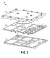
- FIGURE 1 illustrates an example of a currently-available assembly 100 suitable for housing electronics.
- the assembly 100 includes a machined bottom shield 110 and a machined top shield 130, either or both of which have a form-in-place gasket or other gasket.
- the assembly 100 also includes a printed circuit board (PCB) 120 that is positioned and secured between the machined bottom shield 110 and the machined top shield 130.
- PCB printed circuit board
- Embodiments of the disclosed technology generally include an assembly having a printed circuit board (PCB) that is positioned and secured between a top shield and a bottom shield, wherein at least one of the top and bottom shields is a laminated shield.
- PCB printed circuit board
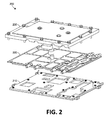
- FIGURE 2 illustrates an example of an assembly 200 suitable for housing electronic components in accordance with certain embodiments of the disclosed technology.
- the assembly 200 includes a printed circuit board (PCB) 220 positioned and secured between a laminated bottom shield 210 and a top shield 230.
- the top shield 230 may be either machined or laminated.
- FIGURE 3 illustrates a more detailed example of the laminated bottom shield 210 illustrated by FIGURE 2 in accordance with certain embodiments of the disclosed technology.
- the bottom shield 210 includes a conductive outer cover 212 that may be attached, e.g., with a laminating material 214 of appropriate construction to match the conductive outer cover 212 and a conductive punched wall section 216.
- a mechanical hardware component 218 may be sized to provide proper spacing between the punched conductive wall section 216 and the PCB 220 so that the chosen gasket material is not over compressed.
- the conductive outer cover 212 may be made of any suitable conductive material, such as punched aluminum, for example.
- the conductive outer cover 212 may be created by techniques other than punching such as laser cutting, water jet cutting, stamping, or other suitable metal cutting process, for example. If additional component height is needed above the height of the punched wall section 216, the outer cover 212 may be dimpled or have secondary parts attached thereto in order to provide the additional height.
- the laminating material 214 is generally selected based on the materials chosen to be laminated as well as the electrical attenuation required.
- appropriate laminating materials that can be used will generally include double-sided conductive adhesive, aluminum solder paste, aluminum solder preforms, conductive epoxy, and sheet gasket with double-sided adhesive, for example.
- laminating methods may include the use of mechanical fasteners such as rivets, spot welds, screws, or PEM hardware to trap a gasket or gasket-like material between the outer cover 212 and the wall section 216.
- the gasket materials used may include dimpled sheet gasket, woven screen, sheet gasket, or dielectric absorber, for example.
- the punched conductive wall section 216 may also be made of any conductive material, such as aluminum, for example. Clearance cavities may be punched to provide space for tall PCB components, e.g. components that cannot fit under the gap provided by the gasket stops. In such cases, the gasket stops may provide .025" clearance above the PCB top layer and the open cavities may provide .125" clearance, for example. Greater or lesser clearance may be provided in other embodiments. Additional clearance may be provided by either using thicker sheet metal or, if needed due to vendor punch press limitations, by laminating multiple wall sections, for example.
- the laminated punched sheet metal approach according to embodiments of the disclosed technology is generally less costly in both the punch process used as well as the time to make the parts. Even in the event that secondary milling operations are required, the savings from elimination of the need to mill the entire shield from a billet of metal is substantial. Due to the cost of milling vs. punched operations, producers tend to procure the milled shields from distant sources, further increasing the time from conception to parts due to shipping. By moving to a punched process, there may be a compelling financial motivation to build the parts locally thus reducing the time from concept to parts.
Landscapes
- Engineering & Computer Science (AREA)
- Microelectronics & Electronic Packaging (AREA)
- Shielding Devices Or Components To Electric Or Magnetic Fields (AREA)
- Casings For Electric Apparatus (AREA)
Abstract
Description
- The present application claims the benefit of
U.S. Provisional Patent Application No. 61/936,585 - The disclosed technology is generally directed toward enclosures or shields for housing electronic components and, more particularly, to such enclosures or shields that include integrated gaskets.
-
FIGURE 1 illustrates an example of a currently-available assembly 100 suitable for housing electronics. Theassembly 100 includes amachined bottom shield 110 and a machinedtop shield 130, either or both of which have a form-in-place gasket or other gasket. Theassembly 100 also includes a printed circuit board (PCB) 120 that is positioned and secured between themachined bottom shield 110 and the machinedtop shield 130. - A major deficiency of an assembly that includes one or more machined shields, such as the
assembly 100 illustrated byFIGURE 1 , is the significant cost needed to machine away so much material to create not only internal cavities and external surfaces of the machined shield but also gasket stops. The machine time needed for this directly results in significantly increased production costs. - Accordingly, a need remains for cost-effective alternatives to assemblies such as the
assembly 100 illustrated byFIGURE 1 . - Embodiments of the disclosed technology generally include an assembly having a printed circuit board (PCB) that is positioned and secured between a top shield and a bottom shield, wherein at least one of the top and bottom shields is a laminated shield.
-
-
FIGURE 1 illustrates an example of a currently-available assembly suitable for housing electronics. -
FIGURE 2 illustrates an example of an assembly suitable for housing electronics in accordance with certain embodiments of the disclosed technology. -
FIGURE 3 illustrates a more detailed example of the laminated bottom shield illustrated byFIGURE 2 in accordance with certain embodiments of the disclosed technology. -
FIGURE 2 illustrates an example of anassembly 200 suitable for housing electronic components in accordance with certain embodiments of the disclosed technology. In the example, theassembly 200 includes a printed circuit board (PCB) 220 positioned and secured between a laminatedbottom shield 210 and atop shield 230. Thetop shield 230 may be either machined or laminated. -
FIGURE 3 illustrates a more detailed example of the laminatedbottom shield 210 illustrated byFIGURE 2 in accordance with certain embodiments of the disclosed technology. In the example, thebottom shield 210 includes a conductiveouter cover 212 that may be attached, e.g., with a laminatingmaterial 214 of appropriate construction to match the conductiveouter cover 212 and a conductive punchedwall section 216. Amechanical hardware component 218 may be sized to provide proper spacing between the punchedconductive wall section 216 and the PCB 220 so that the chosen gasket material is not over compressed. - The conductive
outer cover 212 may be made of any suitable conductive material, such as punched aluminum, for example. In alternative embodiments, the conductiveouter cover 212 may be created by techniques other than punching such as laser cutting, water jet cutting, stamping, or other suitable metal cutting process, for example. If additional component height is needed above the height of the punchedwall section 216, theouter cover 212 may be dimpled or have secondary parts attached thereto in order to provide the additional height. - The laminating
material 214 is generally selected based on the materials chosen to be laminated as well as the electrical attenuation required. Consider an example in which theouter cover 212 andwall section 216 are both constructed from aluminum. In such example, appropriate laminating materials that can be used will generally include double-sided conductive adhesive, aluminum solder paste, aluminum solder preforms, conductive epoxy, and sheet gasket with double-sided adhesive, for example. - Other laminating methods may include the use of mechanical fasteners such as rivets, spot welds, screws, or PEM hardware to trap a gasket or gasket-like material between the
outer cover 212 and thewall section 216. The gasket materials used may include dimpled sheet gasket, woven screen, sheet gasket, or dielectric absorber, for example. - The punched
conductive wall section 216 may also be made of any conductive material, such as aluminum, for example. Clearance cavities may be punched to provide space for tall PCB components, e.g. components that cannot fit under the gap provided by the gasket stops. In such cases, the gasket stops may provide .025" clearance above the PCB top layer and the open cavities may provide .125" clearance, for example. Greater or lesser clearance may be provided in other embodiments. Additional clearance may be provided by either using thicker sheet metal or, if needed due to vendor punch press limitations, by laminating multiple wall sections, for example. - The laminated punched sheet metal approach according to embodiments of the disclosed technology is generally less costly in both the punch process used as well as the time to make the parts. Even in the event that secondary milling operations are required, the savings from elimination of the need to mill the entire shield from a billet of metal is substantial. Due to the cost of milling vs. punched operations, producers tend to procure the milled shields from distant sources, further increasing the time from conception to parts due to shipping. By moving to a punched process, there may be a compelling financial motivation to build the parts locally thus reducing the time from concept to parts.
- Having described and illustrated the principles of the invention with reference to illustrated embodiments, it will be recognized that the illustrated embodiments may be modified in arrangement and detail without departing from such principles, and may be combined in any desired manner. And although the foregoing discussion has focused on particular embodiments, other configurations are contemplated.
- In particular, even though expressions such as "according to an embodiment of the invention" or the like are used herein, these phrases are meant to generally reference embodiment possibilities, and are not intended to limit the invention to particular embodiment configurations. As used herein, these terms may reference the same or different embodiments that are combinable into other embodiments.
- Consequently, in view of the wide variety of permutations to the embodiments that are described herein, this detailed description and accompanying material is intended to be illustrative only, and should not be taken as limiting the scope of the invention. What is claimed as the invention, therefore, is all such modifications as may come within the scope of the following claims and equivalents thereto.
Claims (14)
- An assembly suitable for housing electronic components, the assembly comprising:a top shield; anda bottom shield coupled with the top shield, the bottom shield including:a conductive outer cover;a wall section; anda laminating portion between the conductive outer cover and the wall section, the laminating portion comprising laminating material.
- The assembly of claim 1, wherein the wall section is a conductive punched wall section.
- The assembly of claim 1 or 2, further comprising a printed circuit board, PCB, positioned between the top shield and the bottom shield.
- The assembly of claim 3, further comprising at least one mechanical hardware component configured to provide proper spacing between the wall section of the bottom shield and the PCB.
- The assembly of any preceding claim, wherein the conductive outer cover is made of punched aluminum.
- The assembly of any preceding claim, wherein the conductive outer cover is configured to provide additional height for at least one component on the PCB.
- The assembly of claim 6, wherein the conductive outer cover is dimpled.
- The assembly of claim 6, further comprising secondary parts attached to the conductive outer cover and configured to provide the additional height for the at least one component on the PCB.
- The assembly of any preceding claim, wherein the wall section is constructed from aluminum.
- The assembly of any preceding claim, wherein the laminating material includes at least one from a group consisting of: double-sided conductive adhesive, aluminum solder paste, aluminum solder preforms, conductive epoxy, and sheet gasket with double-sided adhesive.
- The assembly of any preceding claim, further comprising at least one mechanical fastener configured to trap a gasket or gasket-like material between the conductive outer cover and the wall section.
- The assembly of claim 11, wherein the at least one mechanical fastener includes at least one from a group consisting of: rivets, spot welds, screws, and PEM hardware.
- The assembly of claim 11 or 12, wherein gasket-like material includes at least one from a group consisting of: dimpled sheet gasket, woven screen, sheet gasket, and dielectric absorber.
- The assembly of any preceding claim, wherein the wall section includes at least one clearance cavity punched therein to provide extra space for at least one component on the PCB.
Applications Claiming Priority (2)
| Application Number | Priority Date | Filing Date | Title |
|---|---|---|---|
| US201461936585P | 2014-02-06 | 2014-02-06 | |
| US14/286,233 US9439307B2 (en) | 2014-02-06 | 2014-05-23 | Laminated punched sheet metal electronic enclosure/shield with integrated gaskets |
Publications (1)
| Publication Number | Publication Date |
|---|---|
| EP2906031A1 true EP2906031A1 (en) | 2015-08-12 |
Family
ID=52629363
Family Applications (1)
| Application Number | Title | Priority Date | Filing Date |
|---|---|---|---|
| EP15154082.0A Withdrawn EP2906031A1 (en) | 2014-02-06 | 2015-02-06 | Laminated punched sheet metal electronic enclosure/shield with integrated gaskets |
Country Status (4)
| Country | Link |
|---|---|
| US (1) | US9439307B2 (en) |
| EP (1) | EP2906031A1 (en) |
| JP (1) | JP2015149479A (en) |
| CN (1) | CN104837312A (en) |
Families Citing this family (2)
| Publication number | Priority date | Publication date | Assignee | Title |
|---|---|---|---|---|
| US10064317B1 (en) * | 2015-10-27 | 2018-08-28 | Anritsu Company | High isolation shield gasket and method of providing a high isolation shield gasket |
| US20260068112A1 (en) * | 2024-08-29 | 2026-03-05 | Raytheon Company | Localized radiation shielding for space applications |
Citations (9)
| Publication number | Priority date | Publication date | Assignee | Title |
|---|---|---|---|---|
| DE3902998A1 (en) * | 1989-02-02 | 1990-08-16 | Rohde & Schwarz | Housing for microwave-microstrip (stripline) circuits |
| US5252782A (en) * | 1992-06-29 | 1993-10-12 | E-Systems, Inc. | Apparatus for providing RFI/EMI isolation between adjacent circuit areas on a single circuit board |
| US5550713A (en) * | 1995-09-06 | 1996-08-27 | Aironet Wireless Communications, Inc. | Electromagnetic shielding assembly for printed circuit board |
| US5581217A (en) * | 1995-09-21 | 1996-12-03 | Hughes Aircraft Company | Microwave shielding structures comprising parallel-plate waveguide |
| US5604668A (en) * | 1995-12-06 | 1997-02-18 | Motorola, Inc. | Apparatus for shielding electronic circuit boards |
| EP0986293A1 (en) * | 1998-09-08 | 2000-03-15 | Lucent Technologies Inc. | Radio frequency electronic apparatus |
| GB2355595A (en) * | 1999-10-22 | 2001-04-25 | Lucent Technologies Inc | Shielding radio frequency electronic apparatus |
| DE102007048159A1 (en) * | 2007-10-08 | 2009-04-09 | Eubus Gmbh | Housing for accommodating e.g. high frequency plug, has mounting auxiliary boreholes, and covers and frame conductively connected with one another within area of surfaces coated with conductive material |
| CN102802386B (en) * | 2011-05-25 | 2016-04-20 | 莱尔德电子材料(深圳)有限公司 | Electromagnetic interference shield assembly |
Family Cites Families (18)
| Publication number | Priority date | Publication date | Assignee | Title |
|---|---|---|---|---|
| JPH037995Y2 (en) * | 1986-01-17 | 1991-02-27 | ||
| JPS63133600A (en) * | 1986-11-26 | 1988-06-06 | 株式会社日立国際電気 | Shielding structure for electronic equipment |
| JPH01225200A (en) * | 1988-03-03 | 1989-09-08 | Nec Corp | Mounting structure for high frequency circuit unit |
| JPH0738271A (en) * | 1993-07-16 | 1995-02-07 | Nec Kansai Ltd | Transceiver circuit module |
| FI117224B (en) * | 1994-01-20 | 2006-07-31 | Nec Tokin Corp | Electromagnetic piece for removing interference, as well as electronic device and hybrid microcircuit element in which it is used |
| JPH08330772A (en) * | 1995-05-31 | 1996-12-13 | Fujitsu Ltd | Communication device housing structure |
| US6242690B1 (en) * | 1995-09-25 | 2001-06-05 | Ericsson Inc. | Gasket system for EMI isolation |
| JP3840311B2 (en) * | 1997-06-04 | 2006-11-01 | Smk株式会社 | Electromagnetic shield structure |
| JP3965735B2 (en) * | 1997-09-19 | 2007-08-29 | 株式会社富士通ゼネラル | Microwave equipment |
| US6037846A (en) * | 1998-10-09 | 2000-03-14 | Nortel Networks Corporation | Surface mount EMI gasket filter |
| TW456685U (en) * | 2000-03-03 | 2001-09-21 | Hon Hai Prec Ind Co Ltd | Shielding member of mobile phone |
| JP2004072051A (en) * | 2002-08-09 | 2004-03-04 | Kitagawa Ind Co Ltd | Shield structure and forming method thereof |
| JP2004111627A (en) * | 2002-09-18 | 2004-04-08 | Kitagawa Ind Co Ltd | Shield case, shield structure, and method for manufacturing shield case |
| US7326862B2 (en) * | 2003-02-13 | 2008-02-05 | Parker-Hannifin Corporation | Combination metal and plastic EMI shield |
| CN1707698A (en) * | 2004-06-12 | 2005-12-14 | 鸿富锦精密工业(深圳)有限公司 | Electronic device capable of shielding electromagnetic interference |
| US7254034B2 (en) * | 2004-12-15 | 2007-08-07 | Lucent Technologies Inc. | Thermal management for shielded circuit packs |
| US8511229B2 (en) * | 2007-05-09 | 2013-08-20 | Amish Desai | Multilayered microcavities and actuators incorporating same |
| CN201332570Y (en) * | 2008-11-20 | 2009-10-21 | 环隆电气股份有限公司 | Electromagnetic shielding structure |
-
2014
- 2014-05-23 US US14/286,233 patent/US9439307B2/en not_active Expired - Fee Related
-
2015
- 2015-02-05 JP JP2015020918A patent/JP2015149479A/en active Pending
- 2015-02-05 CN CN201510060147.4A patent/CN104837312A/en active Pending
- 2015-02-06 EP EP15154082.0A patent/EP2906031A1/en not_active Withdrawn
Patent Citations (9)
| Publication number | Priority date | Publication date | Assignee | Title |
|---|---|---|---|---|
| DE3902998A1 (en) * | 1989-02-02 | 1990-08-16 | Rohde & Schwarz | Housing for microwave-microstrip (stripline) circuits |
| US5252782A (en) * | 1992-06-29 | 1993-10-12 | E-Systems, Inc. | Apparatus for providing RFI/EMI isolation between adjacent circuit areas on a single circuit board |
| US5550713A (en) * | 1995-09-06 | 1996-08-27 | Aironet Wireless Communications, Inc. | Electromagnetic shielding assembly for printed circuit board |
| US5581217A (en) * | 1995-09-21 | 1996-12-03 | Hughes Aircraft Company | Microwave shielding structures comprising parallel-plate waveguide |
| US5604668A (en) * | 1995-12-06 | 1997-02-18 | Motorola, Inc. | Apparatus for shielding electronic circuit boards |
| EP0986293A1 (en) * | 1998-09-08 | 2000-03-15 | Lucent Technologies Inc. | Radio frequency electronic apparatus |
| GB2355595A (en) * | 1999-10-22 | 2001-04-25 | Lucent Technologies Inc | Shielding radio frequency electronic apparatus |
| DE102007048159A1 (en) * | 2007-10-08 | 2009-04-09 | Eubus Gmbh | Housing for accommodating e.g. high frequency plug, has mounting auxiliary boreholes, and covers and frame conductively connected with one another within area of surfaces coated with conductive material |
| CN102802386B (en) * | 2011-05-25 | 2016-04-20 | 莱尔德电子材料(深圳)有限公司 | Electromagnetic interference shield assembly |
Also Published As
| Publication number | Publication date |
|---|---|
| JP2015149479A (en) | 2015-08-20 |
| CN104837312A (en) | 2015-08-12 |
| US20150223357A1 (en) | 2015-08-06 |
| US9439307B2 (en) | 2016-09-06 |
Similar Documents
| Publication | Publication Date | Title |
|---|---|---|
| US20080259587A1 (en) | Enclosure And Gasket Assembly For Reducing EMI | |
| US10334766B2 (en) | Shield structure | |
| US9439307B2 (en) | Laminated punched sheet metal electronic enclosure/shield with integrated gaskets | |
| CN207531264U (en) | A kind of shielding case and mobile terminal | |
| CN101568251A (en) | Shielding structure | |
| US8507808B2 (en) | Shielding assembly and method for manufacturing same | |
| US20090166081A1 (en) | Electromagnetic shield | |
| US8610003B2 (en) | Shielding plate and shielding assembly with same | |
| CN206181715U (en) | Mobile terminal shield assembly | |
| CN102802386B (en) | Electromagnetic interference shield assembly | |
| US20040211579A1 (en) | One-piece manufactured shielding casing for accommodating electronic functional elements | |
| US8803005B2 (en) | Electromagnetic interference blocking cabinet with integrated input/output panel | |
| CN208242096U (en) | Electronic equipment | |
| US20050237727A1 (en) | Radio frequency shield covers | |
| CN208509368U (en) | Has the electromagnetic wave shielding mask of line windering function | |
| CN202121492U (en) | Power source and power source casing thereof | |
| US9485893B2 (en) | Electrical system with shielding | |
| JP2014063811A (en) | Electronic apparatus | |
| JP2018117083A (en) | Housing for electric apparatus and electric apparatus | |
| CN203197332U (en) | Milling half-bore processing device of PTH (Plated Through Hole) groove for PCB (Printed Circuit Board) | |
| CN105555113A (en) | Shielding cover structure | |
| CN207543498U (en) | Quick detachable pcb board shielding case and pcb board | |
| CN203151902U (en) | Printed circuit board-packaging housing, printed circuit board and apparatus | |
| JP4557740B2 (en) | Electronic equipment and its fireproof enclosure | |
| US20150002995A1 (en) | Keyboard |
Legal Events
| Date | Code | Title | Description |
|---|---|---|---|
| PUAI | Public reference made under article 153(3) epc to a published international application that has entered the european phase |
Free format text: ORIGINAL CODE: 0009012 |
|
| AK | Designated contracting states |
Kind code of ref document: A1 Designated state(s): AL AT BE BG CH CY CZ DE DK EE ES FI FR GB GR HR HU IE IS IT LI LT LU LV MC MK MT NL NO PL PT RO RS SE SI SK SM TR |
|
| AX | Request for extension of the european patent |
Extension state: BA ME |
|
| 17P | Request for examination filed |
Effective date: 20160520 |
|
| RBV | Designated contracting states (corrected) |
Designated state(s): AL AT BE BG CH CY CZ DE DK EE ES FI FR GB GR HR HU IE IS IT LI LT LU LV MC MK MT NL NO PL PT RO RS SE SI SK SM TR |
|
| STAA | Information on the status of an ep patent application or granted ep patent |
Free format text: STATUS: EXAMINATION IS IN PROGRESS |
|
| 17Q | First examination report despatched |
Effective date: 20170503 |
|
| STAA | Information on the status of an ep patent application or granted ep patent |
Free format text: STATUS: THE APPLICATION IS DEEMED TO BE WITHDRAWN |
|
| 18D | Application deemed to be withdrawn |
Effective date: 20200901 |