EP2905901B1 - Circuit assembly and method for detecting a capacity and/or a change in capacity of a capacitive component - Google Patents
Circuit assembly and method for detecting a capacity and/or a change in capacity of a capacitive component Download PDFInfo
- Publication number
- EP2905901B1 EP2905901B1 EP15153534.1A EP15153534A EP2905901B1 EP 2905901 B1 EP2905901 B1 EP 2905901B1 EP 15153534 A EP15153534 A EP 15153534A EP 2905901 B1 EP2905901 B1 EP 2905901B1
- Authority
- EP
- European Patent Office
- Prior art keywords
- voltage
- signal
- output signal
- capacitance
- output
- Prior art date
- Legal status (The legal status is an assumption and is not a legal conclusion. Google has not performed a legal analysis and makes no representation as to the accuracy of the status listed.)
- Active
Links
Images

Classifications
-
- G—PHYSICS
- G01—MEASURING; TESTING
- G01R—MEASURING ELECTRIC VARIABLES; MEASURING MAGNETIC VARIABLES
- G01R27/00—Arrangements for measuring resistance, reactance, impedance, or electric characteristics derived therefrom
- G01R27/02—Measuring real or complex resistance, reactance, impedance, or other two-pole characteristics derived therefrom, e.g. time constant
- G01R27/26—Measuring inductance or capacitance; Measuring quality factor, e.g. by using the resonance method; Measuring loss factor; Measuring dielectric constants ; Measuring impedance or related variables
- G01R27/2605—Measuring capacitance
-
- G—PHYSICS
- G01—MEASURING; TESTING
- G01M—TESTING STATIC OR DYNAMIC BALANCE OF MACHINES OR STRUCTURES; TESTING OF STRUCTURES OR APPARATUS, NOT OTHERWISE PROVIDED FOR
- G01M17/00—Testing of vehicles
-
- H—ELECTRICITY
- H03—ELECTRONIC CIRCUITRY
- H03K—PULSE TECHNIQUE
- H03K17/00—Electronic switching or gating, i.e. not by contact-making and –breaking
- H03K17/94—Electronic switching or gating, i.e. not by contact-making and –breaking characterised by the way in which the control signals are generated
- H03K17/945—Proximity switches
- H03K17/955—Proximity switches using a capacitive detector
-
- H—ELECTRICITY
- H03—ELECTRONIC CIRCUITRY
- H03K—PULSE TECHNIQUE
- H03K17/00—Electronic switching or gating, i.e. not by contact-making and –breaking
- H03K17/94—Electronic switching or gating, i.e. not by contact-making and –breaking characterised by the way in which the control signals are generated
- H03K17/96—Touch switches
- H03K17/962—Capacitive touch switches
-
- H—ELECTRICITY
- H03—ELECTRONIC CIRCUITRY
- H03K—PULSE TECHNIQUE
- H03K2217/00—Indexing scheme related to electronic switching or gating, i.e. not by contact-making or -breaking covered by H03K17/00
- H03K2217/94—Indexing scheme related to electronic switching or gating, i.e. not by contact-making or -breaking covered by H03K17/00 characterised by the way in which the control signal is generated
- H03K2217/96—Touch switches
- H03K2217/9607—Capacitive touch switches
- H03K2217/96071—Capacitive touch switches characterised by the detection principle
- H03K2217/960715—Rc-timing; e.g. measurement of variation of charge time or discharge time of the sensor
-
- H—ELECTRICITY
- H03—ELECTRONIC CIRCUITRY
- H03K—PULSE TECHNIQUE
- H03K2217/00—Indexing scheme related to electronic switching or gating, i.e. not by contact-making or -breaking covered by H03K17/00
- H03K2217/94—Indexing scheme related to electronic switching or gating, i.e. not by contact-making or -breaking covered by H03K17/00 characterised by the way in which the control signal is generated
- H03K2217/96—Touch switches
- H03K2217/9607—Capacitive touch switches
- H03K2217/96071—Capacitive touch switches characterised by the detection principle
- H03K2217/960725—Charge-transfer
Landscapes
- Physics & Mathematics (AREA)
- General Physics & Mathematics (AREA)
- Measurement Of Resistance Or Impedance (AREA)
- Electronic Switches (AREA)
- Amplifiers (AREA)
Description
Die vorliegende Erfindung betrifft eine Schaltungsanordnung und ein Verfahren zur Erfassung einer Kapazität eines kapazitiven Bauelements und/oder einer Änderung der Kapazität eines kapazitiven Bauelements gemäß den Oberbegriffen der Ansprüche 1 und 13.The present invention relates to a circuit arrangement and a method for detecting a capacitance of a capacitive component and / or a change in the capacitance of a capacitive component according to the preambles of
Eine gattungsgemäße Schaltungsanordnung ist aus der
Eine derartige Schaltungsanordnung ist beispielsweise für eine Verstellvorrichtung für ein fremdkraftbetätigt verstellbares Schließelement eines Fahrzeugs einsetzbar, beispielsweise für eine elektromotorisch verstellbare Heckklappe oder Seitentür oder einen elektromotorisch verstellbaren Kofferraumdeckel eines Kraftfahrzeugs. Das kapazitive Bauelement wird hier beispielsweise durch eine Sensorelektrode gebildet, um hierüber berührungslos ein Bedienereignis detektieren zu können. So ändert sich durch ein Körperteil eines Nutzers im Bereich der Sensorelektrode die messbare Kapazität, so dass ein Nutzer durch das jeweilige Körperteil gezielt ein Bedienereignis auslösen kann, das über die Sensorelektrode detektiert wird und zu einer automatischen Verstellung des jeweiligen Schließelements führen soll. Eine beispielhafte Anwendung ist hierbei die Anwendung einer Sensorelektrode im Bereich eines hinteren Stoßfängers eines Kraftfahrzeugs, um über die Sensorelektrode eine Bewegung eines Fußes eines Nutzers im Bereich des Stoßfängers nach Art eines "Kicks" als ein Bedienereignis zu erkennen und in Reaktion hierauf die Heckklappe oder den Kofferraumdeckel des Kraftfahrzeugs zu öffnen. Die Verstellung des Schließelements in Form der Heckklappe oder des Kofferraumdeckels kann somit berührungslos, d. h., ohne Berühren des jeweiligen Schließelements durch den Nutzer gesteuert werden.Such a circuit arrangement can be used, for example, for an adjusting device for a closing element of a vehicle which can be actuated by power, for example for an electromotively adjustable tailgate or side door or an electromotively adjustable trunk lid of a motor vehicle. The capacitive component is formed here, for example, by a sensor electrode in order to be able to detect an operating event without contact. Thus, the measurable capacitance changes through a body part of a user in the area of the sensor electrode, so that a user can specifically trigger an operating event through the respective body part, which is detected via the sensor electrode and is intended to lead to an automatic adjustment of the respective closing element. An exemplary application here is the use of a sensor electrode in the area of a rear bumper of a motor vehicle in order to use the sensor electrode to recognize a user's foot in the area of the bumper as a "kick" as an operating event and in response to this the tailgate or the Open the trunk lid of the motor vehicle. The adjustment of the closing element in the form of the tailgate or the trunk lid can thus be contactless, i. that is, can be controlled by the user without touching the respective closing element.
In der
Das Vorgesehen einer Konstantstromquelle und deren gezielte Schaltung auf Basis des von der monostabilen Kippschaltung bereitgestellten Ausgangssignals beispielsweise über einen in der Schaltungsanordnung vorzusehenden Schalter kann aber unter Umständen schaltungstechnisch nur vergleichsweise aufwendig zu realisieren sein.The provision of a constant current source and its targeted switching on the basis of the output signal provided by the monostable multivibrator, for example via a switch to be provided in the circuit arrangement, can, however, be comparatively complex to implement under certain circumstances.
Aus der
Bei der Schaltungsanordnung der
Eine andere Schaltungsanordnung zur Erfassung einer Kapazität eines kapazitiven Bauelements ist aus der
Der vorliegenden Erfindung liegt damit die Aufgabe zugrunde, eine gattungsgemäße Schaltungsanordnung weiter zu verbessern und ein verbessertes Verfahren zur Erfassung einer Kapazität und/oder einer Kapazitätsänderung eines kapazitiven Bauelements bereitzustellen.The present invention is therefore based on the object of further improving a generic circuit arrangement and of providing an improved method for detecting a capacitance and / or a capacitance change in a capacitive component.
Diese Aufgabe wird mit der Schaltungsanordnung des Anspruchs 1 und einem Verfahren des Anspruchs 13 gelöst.This object is achieved with the circuit arrangement of
Bei einer erfindungsgemäßen Schaltungsanordnung ist dementsprechend vorgesehen:
- eine durch ein Steuerungssignal steuerbare monostabile Kippschaltung mit wenigstens zwei Eingängen und einem Ausgang, wobei ein erster Eingang der monostabilen Kippschaltung für das Steuerungssignal vorgesehen ist, ein zweiter Eingang mit einem kapazitiven Bauelement verbunden ist und bei einer Ansteuerung ein Ausgangssignal an dem Ausgang der monostabilen Kippschaltung erzeugt wird, dessen Zeitdauer von der Kapazität des kapazitiven Bauelements abhängig ist,
- eine Umwandlungseinrichtung, die mit dem Ausgang der monostabilen Kippschaltung verbunden ist und mit einem einen Operationsverstärker aufweisenden Integrierer dazu ausgebildet und vorgesehen ist, ein an dem Ausgang der monostabilen Kippschaltung erzeugtes Ausgangssignal in eine Signalspannung umzuwandeln, deren Verlauf zu der Zeitdauer des Ausgangssignals proportional ist und die sich linear mit der Zeit verändert,
- eine Auswerteeinheit, die mit dem Integrierer der Umwandlungseinrichtung verbunden ist, um die Signalspannung auszuwerten und hieraus wenigstens einen Erfassungswert zu erzeugen, der die Kapazität und/oder eine Änderung der Kapazität des kapazitiven Bauelements anzeigt, und
- über eine zusätzliche, schaltbare Einstellvorrichtung die Höhe der Signalspannung steuern und/oder eine Kennlinie für die Signalspannung (Ss) verändern zu können.
- a monostable multivibrator that can be controlled by a control signal and has at least two inputs and one output, a first input of the monostable multivibrator being provided for the control signal, a second input being connected to a capacitive component and, when activated, generating an output signal at the output of the monostable multivibrator whose duration depends on the capacitance of the capacitive component,
- a conversion device which is connected to the output of the monostable multivibrator and is designed and provided with an integrator having an operational amplifier to convert an output signal generated at the output of the monostable multivibrator into a signal voltage, the course of which is proportional to the duration of the output signal and which changes linearly with time,
- an evaluation unit which is connected to the integrator of the conversion device in order to evaluate the signal voltage and to generate at least one detection value therefrom which indicates the capacitance and / or a change in the capacitance of the capacitive component, and
- to be able to control the level of the signal voltage and / or to change a characteristic curve for the signal voltage (Ss) via an additional, switchable setting device.
Durch die Verwendung eines Integrierers mit einem Operationsverstärker und mit wenigstens einem hierzu parallel geschalteten Kondensator wird an dem Ausgang des Integrierers, mit dem die Auswerteeinheit verbunden ist, eine linear verlaufende Signalspannung erzeugt, die direkt von dem Ausgangssignal der monostabilen Kippschaltung und damit von der Kapazität des kapazitiven Bauelements abhängt. Der Integrierer ist folglich erfindungsgemäß so ausgebildet und zwischen den Ausgang der monostabilen Kippschaltung und die Auswerteeinheit geschaltet, dass ein Ausgangssignal der monostabilen Kippschaltung an einem Verstärkereingang des Operationsverstärkers anliegt und zu einer sich linear mit der Zeit verändernden Signalspannung führt, wobei die Werte, die die Signalspannung annehmen kann, unmittelbar von dem Ausgangssignal abhängig und durch das Ausgangssignal vorgegeben sindBy using an integrator with an operational amplifier and with at least one capacitor connected in parallel to this, a linear signal voltage is generated at the output of the integrator, to which the evaluation unit is connected, which is directly dependent on the output signal of the monostable multivibrator and thus on the capacitance of the capacitive component depends. The integrator is consequently designed according to the invention and connected between the output of the monostable multivibrator and the evaluation unit in such a way that an output signal of the monostable multivibrator is applied to an amplifier input of the operational amplifier and leads to a signal voltage which changes linearly with time, the values representing the signal voltage can assume are directly dependent on the output signal and are predetermined by the output signal
Im Unterschied zu der Schaltungsanordnung der
Dementsprechend wird in einer bevorzugten Ausführungsvariante vorgesehen, dass die monostabile Kippschaltung derart ausgebildet ist, dass ihr Ausgangssignal zwei diskrete Spannungswerte annehmen kann. Beispielsweise variiert der Spannungswert des Ausgangssignals zwischen 0V und einem positiven Spannungswert, beispielsweise in Höhe von 5V, 10V oder 15V.Accordingly, a preferred embodiment variant provides that the monostable multivibrator is designed such that its output signal can assume two discrete voltage values. For example, the voltage value of the output signal varies between 0V and a positive voltage value, for example 5V, 10V or 15V.
Die Höhe der Signalspannung kann in der erfindungsgemäß mit einem Operationsverstärker ausgebildeten Schaltungsanordnung steuerbar sein, vorzugsweise über eine von dem Ausgangssignal unabhängige elektronische Einstellvorrichtung stufenlos oder in vordefinierten Stufen. Derart kann beispielsweise ein durch den Integrierer vorgegebener Verstärkungsfaktor einstellbar sein. Bei Bedarf und je nach Einsatzzweck, gewünschter Sensitivität, Ansprechschwelle und/oder Umgebungsbedingungen kann somit ein Verstärkungsfaktor zwischen Ausgangssignal und Signalspannung angepasst und eine Kennlinie für die auszuwertende Signalspannung verändert werden.The level of the signal voltage can be controllable in the circuit arrangement designed according to the invention with an operational amplifier, preferably via an electronic adjusting device that is independent of the output signal, or in a stepless manner or in predefined steps. In this way, for example, a gain factor specified by the integrator can be set. If required and depending on the intended use, desired sensitivity, response threshold and / or ambient conditions, an amplification factor between the output signal and signal voltage can thus be adjusted and a characteristic curve for the signal voltage to be evaluated can be changed.
In einer Ausführungsvariante wird hierfür der an einen Eingang des Operationsverstärkers zurückgeführte Strom mithilfe einer elektronischen Einstellvorrichtung verändert. Hierdurch lässt sich die Steilheit einer Kennlinie für die Signalspannung in einfacher Weise gezielt verändern, insbesondere die Kennlinie verkippen.In one embodiment variant, the current fed back to an input of the operational amplifier is changed using an electronic setting device. As a result, the steepness of a characteristic curve for the signal voltage can be specifically changed in a simple manner, in particular the characteristic curve can be tilted.
In einem Ausführungsbeispiel ist eine schaltbare Einstellvorrichtung vorgesehen, über die mehrere diskrete Werte für einen Verstärkungsfaktor vorgegeben und auswählbar sind. Über verschiedene Schaltzustände der Einstellvorrichtung können hierbei verschiedene Verstärkungsfaktoren vorgegeben werden. Durch einen veränderten Verstärkungsfaktor erfolgt in einem möglichen Ausführungsbeispiel auch eine Veränderung der Höhe der Signalspannung, insbesondere eine Veränderung eines möglichen, von dem Ausgangssignal unmittelbar abhängigen Maximalwerts der Signalspannung und hiermit wiederum eine Adaption einer Kennlinie für die Signalspannung. Beispielsweise weist eine Einstellvorrichtung wenigstens ein Schaltmittel in Form eines Feldeffekttransistors, vorzugsweise wenigstens zwei Feldeffekttransistoren auf, um elektrisch gesteuert verschiedene Schaltzustände einnehmen zu können.In one exemplary embodiment, a switchable setting device is provided, by means of which a plurality of discrete values for a gain factor are predetermined and can be selected. Different amplification factors can be specified here via different switching states of the setting device. In a possible exemplary embodiment, a change in the magnitude of the signal voltage, in particular a change in a possible maximum value of the signal voltage that is directly dependent on the output signal, and in turn an adaptation of a characteristic curve for the signal voltage takes place by means of a changed amplification factor. For example, an adjusting device has at least one switching means in the form of a field effect transistor, preferably at least two field effect transistors, in order to be able to assume different switching states in an electrically controlled manner.
Weiterhin wird es bevorzugt, wenn das Ausgangssignal der monostabilen Kippschaltung an einem Verstärkereingang des Operationsverstärkers anliegt und das - vorzugsweise zwischen einem Minimalwert und einem Maximalwert variierende - Ausgangssignal
- einen Minimalwert aufweist, der kleiner ist als ein Spannungswert einer Bezugsspannung, die an dem anderen Verstärkereingang des Operationsverstärkers anliegt, und
- einen Maximalwert aufweist, der größer ist als der Spannungswert der Bezugsspannung an dem anderen Verstärkereingang.
- has a minimum value which is smaller than a voltage value of a reference voltage which is present at the other amplifier input of the operational amplifier, and
- has a maximum value that is greater than the voltage value of the reference voltage at the other amplifier input.
Ein Ausgangssignal kann hier folglich zwei unterschiedliche Zustände abbilden und dementsprechend zwei unterschiedliche Spannungen an einem Verstärkereingang des Operationsverstärkers vorgeben, von denen eine Spannung unterhalb und die andere Spannung oberhalb der an dem anderen Verstärkereingang anliegenden Bezugsspannung liegt. In dieser Konfiguration wird mit einem zu dem Operationsverstärker parallel geschalteten Kondensator, der einerseits mit dem Verstärkereingang verbunden ist, an dem das Ausgangssignal anliegt, und andererseits mit dem Ausgang des Operationsverstärkers verbunden ist, am Ausgang des Operationsverstärkers ein linear ansteigendes oder linear abfallendes Spannungssignal erzeugt, je nachdem, ob die Spannung des Ausgangssignals über oder unterhalb der Bezugsspannung liegt. Hierdurch ist besonders einfach und effektiv ein Rückschluss auf die Kapazität des kapazitiven Bauelements möglich. Da die Dauer des Ausgangssignals mit einem bestimmten Spannungswert unmittelbar von der Kapazität des kapazitiven Bauelements abhängt, ist auch die Dauer des linearen Anstiegs oder Abfalls der Signalspannung stets unmittelbar von der Kapazität des kapazitiven Bauelements abhängig.An output signal can consequently represent two different states and accordingly specify two different voltages at an amplifier input of the operational amplifier, of which one voltage is below and the other voltage is above the reference voltage present at the other amplifier input. In this configuration, a capacitor connected in parallel to the operational amplifier, which is connected on the one hand to the amplifier input to which the output signal is present and on the other hand is connected to the output of the operational amplifier, generates a linearly rising or falling voltage signal at the output of the operational amplifier, depending on whether the voltage of the output signal is above or below the reference voltage. This makes it particularly simple and effective to draw a conclusion about the capacitance of the capacitive component. Because the duration of the output signal with a certain voltage value is directly dependent on the capacitance of the capacitive Depends on the component, the duration of the linear rise or fall of the signal voltage is always directly dependent on the capacitance of the capacitive component.
Im Hinblick auf eine möglichst ökonomische Schaltungsanordnung wird es bevorzugt, dass zum Betrieb des Operationsverstärkers eine Versorgungsspannung vorgesehen ist und die Schaltungsanordnung einen Spannungsteiler aufweist, um eine Bezugsspannung, die an einem Verstärkereingang des Operationsverstärkers anliegt, als eine Teilspannung dieser Versorgungsspannung bereitzustellen. Damit kann an einer Stelle der Schaltungsanordnung die Versorgungsspannung angelegt werden und hieran nicht nur ein Versorgungsanschluss des Operationsverstärkers angeschlossen werden, sondern auch über einen Spannungsteiler einer der Verstärkereingänge des Operationsverstärkers. Wie allgemein bekannt wird ein solcher Spannungsteiler bevorzugt durch zwei Widerstände gebildet.With regard to a circuit arrangement that is as economical as possible, it is preferred that a supply voltage is provided for operating the operational amplifier and that the circuit arrangement has a voltage divider in order to provide a reference voltage that is present at an amplifier input of the operational amplifier as a partial voltage of this supply voltage. The supply voltage can thus be applied at one point in the circuit arrangement and not only a supply connection of the operational amplifier can be connected thereto, but also via a voltage divider of one of the amplifier inputs of the operational amplifier. As is generally known, such a voltage divider is preferably formed by two resistors.
In einer bevorzugten Ausführungsvariante ist der mit dem Operationsverstärker definierte Integrierer einer erfindungsgemäßen Schaltungsanordnung invertierend ausgestaltet. Dementsprechend liegt hier das Ausgangssignal an dem invertierendem (negativen) Verstärkereingang des Operationsverstärkers an und die Bezugsspannung an dem nicht-invertierendem (positiven) Verstärkereingang. Es ist aber selbstverständlich möglich, auch einen nicht-invertierendem Integrierer zu verwenden, wodurch sich beispielsweise bei gleichbleibenden, zwischen zwei Spannungswerten variierenden Ausgangssignalen lediglich lineare Verläufe für die Signalspannung ergeben, die zu den Verläufen der Signalspannung bei einem invertierendem Integrierer umgekehrt sind.In a preferred embodiment variant, the integrator of a circuit arrangement according to the invention defined with the operational amplifier is designed to be inverting. Accordingly, the output signal is present at the inverting (negative) amplifier input of the operational amplifier and the reference voltage at the non-inverting (positive) amplifier input. However, it is of course also possible to use a non-inverting integrator, which, for example, only results in linear curves for the signal voltage when output signals remain the same, varying between two voltage values, which are reversed to the curves of the signal voltage in the case of an inverting integrator.
Im Hinblick auf die Auswertung der erzeugten Signalspannung wird es in einem Ausführungsbeispiel bevorzugt, dass dem Integrierer ein Spitzenwerthaltglied nachgeschaltet ist, um einen maximalen Spannungswert für die Signalspannung (für das soeben an die monostabile Kippschaltung gegebene Steuerungssignal) zu speichern. Der gehaltene bzw. gespeicherte maximale Spannungswert kann dann beispielsweise mit einem in der Auswerteeinheit hinterlegten Schwellwert für die Signalspannung verglichen werden, um zu bewerten, ob dieser Schwellwert unter- oder überschritten wurde.With regard to the evaluation of the generated signal voltage, it is preferred in one exemplary embodiment that a peak value holding element is connected downstream of the integrator in order to store a maximum voltage value for the signal voltage (for the control signal just given to the monostable multivibrator). The held or stored maximum voltage value can then be compared, for example, with a threshold value for the signal voltage stored in the evaluation unit in order to assess whether this threshold value has been exceeded or fallen short of.
Wird ein Über- oder Unterschreiten des Schwellwerts festgestellt, kann die Auswerteeinheit beispielsweise ein Auslösesignal erzeugen, um zu signalisieren, dass die Kapazität des kapazitiven Bauelements einen als relevant eingestuften Kapazitätswert unterschritten oder überschritten hat bzw. eine entsprechenden Kapazitätsänderung aufgetreten ist. Ein solches Auslösesignal kann beispielsweise das Vorliegen eines Bedienereignisses zur Verstellung eines Schließelements an einem Fahrzeug anzeigen.If an exceeding or falling below the threshold value is determined, the evaluation unit can, for example, generate a trigger signal in order to signal that the capacitance of the capacitive component is classified as relevant Has fallen below or exceeded the capacity value or a corresponding change in capacity has occurred. Such a trigger signal can indicate, for example, the presence of an operating event for adjusting a closing element on a vehicle.
Bei dem an dem Spitzenwerthaltglied gespeicherten maximalen Spannungswert kann es sich somit um einen Erfassungswert handeln, der die Kapazität und/oder eine Änderung der Kapazität des kapazitiven Bauelements anzeigt, so dass das Spitzenwerthalteglied hier Teil einer (elektronischen) Auswerteeinheit darstellt. Alternativ oder ergänzend kann selbstverständlich auch die Signalspannung direkt an eine elektronische Auswerteeinheit übertragen werden. Die Auswerteeinheit ist hierbei beispielsweise dazu in der Lage, anhand des Signalverlaufs, insbesondere zum Beispiel anhand der Dauer eines linearen Anstiegs oder Abfalls der Signalspannung bis zum Über- und/oder Unterschreiten eines Schwellwerts oder sogar mehrerer Schwellwerte einen Erfassungswert oder mehrere Erfassungswerte zu gewinnen. Ein Erfassungswert kann beispielsweise einer nachgeschalteten Steuerungseinrichtung eine Kapazität des kapazitiven Bauelements und/oder eine Kapazitätsänderung anzeigen. So kann es sich bei dem Erfassungswert auch um einen Wert handeln, der von der Auswerteeinheit generiert wird, um einen bestimmten Kapazitätswert und/oder eine Kapazitätswertänderung bei dem kapazitiven Bauelement qualitativ oder quantitativ anzuzeigen.The maximum voltage value stored on the peak value holding element can thus be a detection value which indicates the capacitance and / or a change in the capacitance of the capacitive component, so that the peak value holding element here forms part of an (electronic) evaluation unit. Alternatively or in addition, the signal voltage can of course also be transmitted directly to an electronic evaluation unit. In this case, the evaluation unit is able, for example, to obtain a detection value or a plurality of detection values on the basis of the signal curve, in particular, for example, on the basis of the duration of a linear rise or fall in the signal voltage until a threshold value or even a number of threshold values are exceeded or not reached. A detection value can, for example, indicate to a downstream control device a capacitance of the capacitive component and / or a change in capacitance. Thus, the detection value can also be a value that is generated by the evaluation unit in order to indicate qualitatively or quantitatively a specific capacitance value and / or a change in capacitance value in the capacitive component.
In einer beispielhaften Schaltungsanordnung umfasst das Spitzenwerthalteglied, das mit dem Ausgang des Integrierers verbunden ist, wenigstens eine Diode und einen Speicherkondensator. Es ist selbstverständlich möglich, dass der an dem Spitzenwerthalteglied gehaltene maximale Spannungswert nicht identisch zu einem Maximalwert der an dem Ausgang des Integrierers erzeugten Signalspannung ist. So können beispielsweise in der Schaltungsanordnung noch zusätzliche Widerstände vorgesehen sein, so dass die an dem Speicherkondensator des Spitzenwerthalteglieds mithilfe der Diode gehaltene Spannung geringer ist als die am Ausgang des Integrierers erzeugte Signalspannung. Die an dem Speicherkondensator des Spitzenwerthalteglieds anliegende Spannung ist aber im jeden Fall proportional zu der Signalspannung.In an exemplary circuit arrangement, the peak hold element, which is connected to the output of the integrator, comprises at least one diode and a storage capacitor. It is of course possible that the maximum voltage value held at the peak value holding element is not identical to a maximum value of the signal voltage generated at the output of the integrator. For example, additional resistances can be provided in the circuit arrangement, so that the voltage held on the storage capacitor of the peak value holding element with the aid of the diode is lower than the signal voltage generated at the output of the integrator. However, the voltage applied to the storage capacitor of the peak value holding element is in any case proportional to the signal voltage.
Wie bereits eingangs erläutert, ist ein weiterer Aspekt der vorliegenden Erfindung die Bereitstellung einer erfindungsgemäßen Schaltungsanordnung in einer Verstellvorrichtung für ein verstellbares Schließelement eines Fahrzeugs.As already explained at the beginning, a further aspect of the present invention is the provision of a circuit arrangement according to the invention in an adjustment device for an adjustable locking element of a vehicle.
Bei einer derartigen Verstellvorrichtung ist über das Schließelement eine Karosserieöffnung eines Fahrzeugs verschließbar und das Schließelement kann zum Freigeben der Karosserieöffnung bei Vorliegen eines Bedienereignisses automatisch verstellbar sein. Alternativ oder ergänzend kann bei Vorliegen eines Bedienereignisses eine Verriegelung des Schließelements betätigbar sein, um das Schließelement freizugeben und überhaupt erst (manuell oder fremdkraftbetätigt) verstellen zu können. Beispielsweise handelt es sich bei dem Schließelement um eine Heckklappe oder eine (Seiten-)Tür eines Kraftfahrzeugs oder einen Kofferraumdeckel eines Kraftfahrzeugs. Über eine kapazitiv arbeitende Sensoreinrichtung mit wenigstens einem kapazitiven Bauelement, zum Beispiel in Form einer einzelnen Sensorelektrode oder wenigstens einem Sensorelektrodenpaar, wird hierbei das Vorliegen eines Bedienereignisses anhand der Kapazität des Bauelements und/oder einer Änderung der Kapazität des Bauelements erkannt.In such an adjusting device, a body opening of a vehicle can be closed via the closing element and the closing element can be automatically adjustable to release the body opening when an operating event is present. Alternatively or additionally, when an operating event is present, a locking of the closing element can be actuated in order to release the closing element and to be able to adjust it at all (manually or powered). For example, the closing element is a tailgate or a (side) door of a motor vehicle or a trunk lid of a motor vehicle. Via a capacitively operating sensor device with at least one capacitive component, for example in the form of a single sensor electrode or at least one pair of sensor electrodes, the presence of an operating event is recognized on the basis of the capacitance of the component and / or a change in the capacitance of the component.
Ein weiterer Aspekt der vorliegenden Erfindung ist ein Verfahren zur Erfassung einer Kapazität und/oder einer Änderung der Kapazität eines kapazitiven Bauelements, bei dem wenigstens die nachfolgenden Schritte vorgesehen sind:
- Steuern einer monostabilen Kippschaltung durch Anlegen eines Steuerungssignals, das beispielsweise von einer elektronisches Steuerungseinheit bereitgestellt wird, an einem ersten Eingang der monostabilen Kippschaltung, wobei die monostabile Kippschaltung an einem zweitem Eingang mit dem kapazitiven Bauelement verbunden ist,
- Erzeugen wenigstens eines Ausgangssignals an einem Ausgang der monostabilen Kippschaltung bei Anlegen des Steuerungssignals, wobei die Zeitdauer des erzeugten Ausgangssignals von der Kapazität des kapazitiven Bauelements abhängig ist, und
- Umwandeln des wenigstens einen Ausgangssignals in eine Signalspannung, deren Verlauf zu der Zeitdauer des Ausgangssignals proportional ist.
- Controlling a monostable multivibrator by applying a control signal, which is provided, for example, by an electronic control unit, to a first input of the monostable multivibrator, the monostable multivibrator being connected to the capacitive component at a second input,
- Generating at least one output signal at an output of the monostable multivibrator when the control signal is applied, the duration of the generated output signal being dependent on the capacitance of the capacitive component, and
- Converting the at least one output signal into a signal voltage, the course of which is proportional to the duration of the output signal.
In Analogie zu einer erfindungsgemäßen Schaltungsanordnung ist bei einem erfindungsgemäßen Verfahren vorgesehen, dass das Umwandeln des Ausgangssignals mittels eines Integrierers erfolgt, der einen Operationsverstärker aufweist, an dessen einem Verstärkereingang das Ausgangssignal anliegt, und der das Ausgangssignal der monostabilen Kippschaltung zu einer sich linear mit der Zeit verändernden Signalspannung umwandelt, so dass die Werte, die die Signalspannung annehmen kann, durch das Ausgangssignal vorgegeben sind. Ferner ist wird erfindungsgemäß eine Möglichkeit zur Steuerung der Höhe der Signalspannung und/oder zur Veränderung eine Kennlinie für die Signalspannung mittels einer schaltbaren Einstellvorrichtung vorgesehen, so dass beispielsweise ein durch den Integrierer vorgegebener Verstärkungsfaktor zwischen Ausgangssignal und Signalspannung stufenlos oder in vordefinierten Stufen einstellbar ist, um diesen bei Bedarf und je nach Einsatzzweck, gewünschter Sensitivität, Ansprechschwelle und/oder Umgebungsbedingungen ohne Weiteres gezielt anzupassen und gegebenenfalls eine Kennlinie für die auszuwertende Signalspannung zu verändern.In analogy to a circuit arrangement according to the invention, it is provided in a method according to the invention that the conversion of the output signal is carried out by means of an integrator which has an operational amplifier to whose one amplifier input the output signal is present, and which the output signal of the monostable multivibrator is linear with time changing Converts signal voltage so that the values that the signal voltage can assume are predetermined by the output signal. Furthermore, according to the invention, a possibility for controlling the level of the signal voltage and / or for changing a characteristic curve for the signal voltage is provided by means of a switchable setting device, so that, for example, a gain factor specified by the integrator between the output signal and the signal voltage can be set continuously or in predefined steps if necessary and depending on the intended use, desired sensitivity, response threshold and / or ambient conditions, it can be readily adapted in a targeted manner and, if necessary, a characteristic curve for the signal voltage to be evaluated can be changed.
Es ist somit offensichtlich, dass die zuvor und nachfolgend noch erläuterten Vorteile und Merkmale von Ausführungsbeispielen einer Schaltungsanordnung auch für ein Verfahren zur Erfassung einer Kapazität und/oder einer Veränderung der Kapazität eines kapazitiven Bauelements gelten und umgekehrt.It is therefore obvious that the advantages and features of exemplary embodiments of a circuit arrangement which have been explained above and below also apply to a method for detecting a capacitance and / or a change in the capacitance of a capacitive component and vice versa.
Bei der nachfolgenden Beschreibung eines Ausführungsbeispiels anhand der Figuren werden weitere Vorteile und Merkmale der vorliegenden Erfindung deutlich werden.Further advantages and features of the present invention will become clear in the following description of an exemplary embodiment using the figures.
Hierbei zeigen:
- Fig. 1
- einen Ausschnitt eines Ausführungsbeispiels für eine Schaltungsanordnung mit einem einen Operationsverstärker aufweisenden invertierenden Integrierer und einem Spitzenwerthalteglied;
- Fig. 2
- eine erfindungsgemäße Weiterbildung des Ausführungsbeispiels der
Figur 1 mit einer Einstellvorrichtung zur Vorgabe unterschiedlicher Verstärkungsfaktoren an dem Integrierer; - Fig. 3
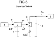
- eine aus dem Stand der Technik bekannte Schaltungsanordnung.
- Fig. 1
- a section of an embodiment of a circuit arrangement with an inverting integrator having an operational amplifier and a peak value holding element;
- Fig. 2
- a development of the embodiment of the invention
Figure 1 with an adjusting device for specifying different gain factors on the integrator; - Fig. 3
- a circuit arrangement known from the prior art.
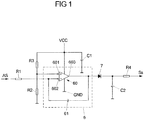
Zunächst Bezug nehmend auf die
Bei dem aus dem Stand der Technik bekannten Ausführungsbeispiel einer Schaltungsanordnung gemäß der
Mittels der monostabilen Kippschaltung 2 wird an einem Ausgang 2.4 der Kippschaltung 2 in Folge eines Steuerungssignals der Steuereinheit 1 wenigstens ein Ausgangssignal AS erzeugt, dessen Zeitdauer von der Kapazität bzw. der Größe der Sensorkapazität 3 abhängig ist. Dieses Ausgangssignal AS wird bei der aus dem Stand der Technik bekannten Schaltungsanordnung zur Steuerung eines Schalters S genutzt, um eine Konstantstromquelle KSQ für die Dauer des Ausgangssignals an einen Integrator 4 in Form eines Kondensators anzuschließen. Über die Konstantstromquelle KSQ wird der Integrator 4 aufgeladen, wobei die über dem Integrator 4 aufintegrierte Spannung als eine Signalspannung Ss von einer elektronischen Auswerteeinheit 5 ausgewertet wird. Die Signalspannung Ss ist zu der Zeitdauer des Ausgangssignals AS proportional und verläuft aufgrund der Konstantstromquelle KSQ linear über die Zeit. Die Signalspannung Ss ist damit repräsentativ für die Größe der Sensorkapazität 3 beziehungsweise die Kapazität und/oder eine Änderung der Kapazität eines hiermit gebildeten Sensorkondensators. Nach dem Abschluss einer Messung ist jeweils ein Entladevorgang vorgesehen.By means of the
Die Auswerteeinheit 5 kann somit aus der Signalspannung Ss einen Erfassungswert bilden, der die Größe der Sensorkapazität 3 quantitativ und/oder die eine Veränderung der Sensorkapazität 3 qualitativ anzeigt. In der Auswerteeinheit 5 ist beispielsweise wenigstens ein Schwellwert hinterlegt, dessen Über- oder Unterschreiten durch die Signalspannung Ss die Erzeugung eines Auslösesignals hervorruft. Ein solches Auslösesignal könnte das Vorliegen eines Bedienereignisses anzeigen, auf das hin eine fremdkraftbetätigte. dass heißt, insbesondere über einen Antriebsmotor angetriebene, Verstellung eines Schließelements eines Fahrzeugs erfolgt. Beispielsweise kann bei Vorliegen eines bestimmten durch die Sensorkapazität 3 sensierten Bedienereignisses ein Öffnen oder Schließen einer Heckklappe oder einer Seitentür und/oder eines Kofferraumdeckels eines Kraftfahrzeugs ausgelöst werden.The
Anstatt die Konstantstromquelle KSQ über den Schalter S selektiv in Abhängigkeit von dem Auslösesignal AS mit dem Integrator 4 zu verschalten, kann alternativ auch vorgesehen sein, dass die Konstantstromquelle KSQ direkt über das Auslösesignal AS ein- und ausgeschaltet wird.Instead of selectively interconnecting the constant current source KSQ via the switch S as a function of the trigger signal AS with the
Die aus der
Mit der erfindungsgemäßen Lösung werden eine verbesserte Schaltungsanordnung und ein verbessertes Verfahren zur Erfassung einer Kapazität und/oder einer Änderung der Kapazität eines kapazitiven Bauelements wie der Sensorkapazität 3 bereitgestellt.With the solution according to the invention, an improved circuit arrangement and an improved method for detecting a capacitance and / or a change in the capacitance of a capacitive component such as the
In der
Das Ausgangssignal AS wird hierbei über einen Widerstand R1 direkt auf einen invertierenden (negativen) Verstärkereingang 602 des Operationsverstärkers 60 gegeben. An dem anderen nicht-invertierenden (positiven) Verstärkereingang 601 des Operationsverstärkers 60 liegt eine Bezugsspannung an, die sich als Teilspannung einer Versorgungsspannung VCC ergibt. Hierfür ist ein durch zwei in Reihe geschaltete Widerstände R2 und R3 gebildeter Spannungsteiler vorgesehen, durch den an dem nicht invertierendem Verstärkereingang 601 nur ein Bruchteil der Versorgungsspannung VCC, zum Beispiel 1/2 VCC, anliegt. Die gegenüber Erde GND angegebene Versorgungsspannung VCC dient ferner auch der Versorgung des Operationsverstärkers 60 und ist folglich mit dessen Versorgungsanschluss verbunden. Zusätzlich ist ein Speicherkondensator C1 vorgesehen, der gegen Erde GND an der Versorgungsspannung VCC anliegt. Über diesen optionalen Speicherkondensator C1 wird eine Stabilisierung der Betriebsspannung, insbesondere für den Operationsverstärker 60 erreicht.The output signal AS is fed via a resistor R1 directly to an inverting (negative)
Zu dem Operationsverstärker 60 ist ferner eine Kapazität 61 in an sich bekannter Weise parallel geschaltet und hierfür sowohl mit einem Ausgang 603 des Operationsverstärkers 60 als auch mit dem invertierendem Verstärkereingang 602 verbunden, an dem das Ausgangssignal AS anliegt.Furthermore, a
Die monostabile Kippschaltung 2 ist hier so ausgeführt, dass in Folge eines Steuerungssignals an ihrem ersten Eingang 2.1 ein Ausgangssignal AS mit einem maximalen (konstanten) Spannungswert >0V, zum Beispiel 5V, erzeugt wird. In Abhängigkeit von der Größe der Sensorkapazität 3 liegt dieses Ausgangssignal AS mit seinem Maximalwert (High-Pegel) für eine bestimmte Dauer an dem invertierenden Verstärkereingang 602 an. Die Bezugsspannung an dem nicht invertierendem Verstärkereingang 601 ist nun so gewählt, dass sie kleiner ist als der maximale Spannungswert des Ausgangssignals AS, beispielsweise in etwa die Hälfte des Maximalwert des Ausgangssignals AS beträgt, also zum Beispiel 2,5V. Dementsprechend wird an dem Verstärkerausgang 603 eine linear über die Zeit abfallende Signalspannung Ss erzeugt, die bis auf 0V absinken kann, je nachdem, wie lange das Ausgangssignal AS mit dem maximalen Spannungswert anliegt.The
Das Ausgangssignal As kann neben seinem Maximalwert auch einen diskreten Minimalwert (Low-Pegel) annehmen, dessen Dauer ebenfalls von der Größe der Sensorkapazität 3 abhängt. Dieser Minimalwert ist vorliegend 0V, so dass somit folglich an dem invertierendem Verstärkereingang 602 eine kleinere Spannung anliegt als an dem nicht-invertierendem Verstärkereingang 601, an dem stets die konstante Bezugsspannung anliegt, die größer ist als der Minimalwert des Ausgangssignals AS (>0 V) und gleichzeitig kleiner als der Maximalwert des Ausgangssignals AS (< 5V). Für eine Bezugspannung VBezug gilt hier somit zum Bespiel 0V < VBezug < 5V.In addition to its maximum value, the output signal As can also assume a discrete minimum value (low level), the duration of which also depends on the size of the
An dem Verstärkerausgang 603 wird in dieser Konstellation eine linear über die Zeit ansteigende Signalspannung Ss erzeugt, deren Dauer ebenfalls direkt proportional zur Dauer des Ausgangssignals AS mit dem Minimalwert und damit abhängig von der Größe der Sensorkapazität 3 ist. Anhand der derart über den Integrierer 6 mit dem Operationsverstärker 60 erzeugten Signalspannung Ss kann somit durch die Auswerteeinheit 5 direkt auf die Größe der Sensorkapazität 3 und/oder eine Änderung der Sensorkapazität 3 qualitativ und/oder quantitativ geschlossen werden.In this constellation, a signal voltage Ss rising linearly over time is generated at the
Im vorliegenden Fall wird sich das Ausgangssignal AS mit dem Minimalwert von hier 0V und der sich daraus ergebenden linear ansteigenden Signalspannung Ss zunutze gemacht, um auf das Vorliegen eines bestimmten Bedienereignisses zu schließen. Dabei wird das Vorliegen eines bestimmten Bedienereignisses detektiert, wenn die Signalspannung Ss ausreichend Zeit hat, über einen Schwellwert hinaus anzusteigen. Das Ausgangssignal AS der monostabilen Kippschaltung 2 mit dem minimalen (gleichbleibenden) Spannungswert von 0V liegt hier also solange an dem Operationsverstärker 60 an, dass die an dem Verstärkerausgang 603 erzeugte Signalspannung Ss über eine durch den Schwellwert definierte Ansprechschwelle hinaus linear ansteigt, was als das Vorliegen eines Bedienereignisses bewertet wird. In Folge des Detektierens dieses Bedienereignisses wird vorliegend bevorzugt ein Auslösesignal durch die Auswerteeinheit 5 erzeugt, um hier ein nicht dargestelltes Schließelement, wie zum Beispiel eine Heckklappe oder einen Kofferraumdeckel eines Kraftfahrzeugs, fremdkraftbetätigt zu öffnen oder zu schließen. Eine über die Sensorkapazität 3 detektierte Änderung eines Kapazitätswertes, die repräsentativ für das Vorliegen eines Bedienereignisses ist, kann dabei beispielsweise durch die Annäherung eines Körperteils eines Benutzer an die Sensorkapazität 3 hervorgerufen worden sein.In the present case, the output signal AS with the minimum value of here 0V and the resulting linearly increasing signal voltage Ss is used in order to conclude that a certain operator event is present. The presence of a certain operating event is detected when the signal voltage Ss has sufficient time to rise above a threshold value. The output signal AS of the
Um bei der Schaltungsanordnung der
Mit der Schaltungsanordnung der
In der
Die Schaltungsanordnung der
Die Einstellvorrichtung 8 kann vorliegend mehrere unterschiedliche Schaltzustände einnehmen, in denen jeweils ein anderer Gesamtwiderstand zu dem Widerstand R5 in Reihe geschaltet ist. Die unterschiedlichen Schaltzustände werden vorliegend über zwei MOSFETs 81 und 82 (MOSFET=Metall-Oxid-Halbleiter-Feldeffekttransistor) vorgegeben. Durch die an dem jeweiligen MOSFET 81 und 82 angelegte Gate-Source- bzw. Steuerspannung U81 oder U82 kann der über den jeweils zugeordneten Widerstand R7 oder R8 fließenden Strom gesteuert werden, wodurch der zu dem Widerstand R5 in Reihe geschaltete Gesamtwiderstand in seiner Größe gezielt veränder- und steuerbar ist. Hierdurch kann auf einfache Weise ein Maximalwert für die Signalspannung Ss variiert, z.B. zwischen 2,5V und 3,5V herauf- oder herabgesetzt und damit die Steilheit der Signalspannung Ss angepasst werden. Ein Schaltzustand der Einstellvorrichtung 8 ist hierbei - im Unterschied zu der Signalspannung Ss - nicht unmittelbar von dem Ausgangssignal AS abhängig, sondern hiervon unabhängig und frei, je nach Bedarf und insbesondere (aktuellem) Verwendungszweck oder Umgebungsbedingungen der Schaltungsanordnung auswählbar.In the present case, the
Die MOSFETs 81 und 82 werden in dem Ausführungsbeispiel der
Obwohl in den Ausführungsbeispielen der
- 11
- Steuereinheitcontrol unit
- 22
- Kippschaltungflop
- 2.1, 2.32.1, 2.3
- Eingangentrance
- 2.42.4
- Ausgangexit
- 33
- Sensorkapazitätsensor capacitance
- 44
- Integratorintegrator
- 55
- Auswerteeinheitevaluation
- 66
- Integriererintegrator
- 6060
- Operationsverstärkeroperational amplifiers
- 601, 602601, 602
- Verstärkereingangamplifier input
- 603603
- Verstärkerausgangamplifier output
- 6161
- Kapazitätcapacity
- 77
- Diodediode
- 88th
- Einstellvorrichtungadjustment
- 8080
- Anschlussleitungconnecting cable
- 81, 8281, 82
- MOSFET (Feldeffekttransistor)MOSFET (field effect transistor)
- ASAS
- Ausgangssignaloutput
- C1C1
- Speicherkondensatorstorage capacitor
- C2C2
- Speicherkondensatorstorage capacitor
- GNDGND
- Erdeearth
- KK
- Knotennode
- KSQKSQ
- KonstantstromquelleConstant current source
- R1 - R8R1 - R8
- Widerstandresistance
- SS
- Schaltercounter
- Ssss
- Signalspannungsignal voltage
- U81, U82 U 81 , U 82
- Steuerspannungcontrol voltage
- VCCVCC
- Versorgungsspannungsupply voltage
Claims (13)
- A circuit arrangement for detecting a capacitance of a capacitive component and/or a change in the capacitance of a capacitive component, comprising- a monostable flipflop (2) controllable by a control signal and having at least two inputs (2.1, 2.3) and one output (2.4), wherein a first input (2.1) of the flipflop (2) is provided for the control signal,- a capacitive component (3), which is connected to a second input (2.3) of the monostable flipflop (2),- a conversion device, which is connected to the output (2.4) of the monostable flipflop (2) and is designed and intended for converting an output signal (AS) generated at the output (2.4) into a signal voltage (Ss), and- an evaluation unit (5), which is connected to the conversion device in order to evaluate the signal voltage (Ss) and from this to generate at least one detection value, which indicates the capacitance and/or a change in the capacitance of the capacitive component (3),wherein the monostable flipflop (2) is designed to generate at least one output signal (AS) at its output (2.4) on actuation by a control signal, the duration of said output signal being dependent on the capacitance of the capacitive component (3), and the conversion device converts the at least one output signal (AS) into a signal voltage (Ss), whose course is proportional to the duration of the output signal (AS),
wherein the conversion device comprises an integrator (6) having an operational amplifier (60), and the integrator (6) is designed and connected between the output (2.4) of the monostable flipflop (2) and the evaluation unit (5) in such a way that an output signal (AS) of the monostable flipflop (2) is present at an amplifier input (602) of the operational amplifier (60) and results in a signal voltage (Ss) which changes linearly over time, wherein the values which can be assumed by the signal voltage (Ss) are preset by the output signal (AS) and dependent directly from the output signal (AS),
characterized in that
the magnitude of the signal voltage (Ss) is controllable and/or a characteristic for the signal voltage (Ss) is variable via a switchable setting device (8) whose switching state is independent from the output signal (AS), the magnitude of the signal voltage (Ss) being controllable and/or the characteristic for the signal voltage (Ss) being variable by setting a gain of the integrator (6) between the output signal generated at the output (2.4) of the monostable flipflop (2) and the signal voltage (Ss) generated via the conversion device (8). - The circuit arrangement according to Claim 1, characterized in that a plurality of discrete values for the gain are preset and selectable via a switchable setting device (8).
- The circuit arrangement according to Claim 1, characterized in that the setting device (8) is provided at an output of the operational amplifier (60) and a current fed back to the operational amplifier (60) can be varied by the switchable setting device (8).
- The circuit arrangement according to Claim 1 to 3, characterized in that the setting device (8) having at least one field-effect transistor (81, 82) for controlling the magnitude of the signal voltage (Ss) and/or a change in the signal voltage(Ss).
- The circuit arrangement according to one of the preceding claims, characterized in that the monostable flipflop (2) is designed in such a way that its output signal (AS) can assume two discrete voltage values.
- The circuit arrangement according to one of the preceding claims, characterized in that the output signal (AS) of the monostable flipflop (2)- has a minimum value, which is less than a voltage value of a reference voltage which is present at the other amplifier input (601) of the operational amplifier (60), and- has a maximum value which is greater than the voltage value of the reference voltage at the other amplifier input (601).
- The circuit arrangement according to one of the preceding claims, characterized in that, for operation of the operational amplifier (60), a supply voltage (VCC) is provided and the circuit arrangement has a voltage divider (R2, R3) in order to provide a reference voltage which is present at an amplifier input (601) of the operational amplifier (60) as a partial voltage of the supply voltage (VCC).
- The circuit arrangement according to one of the preceding claims, characterized in that the integrator (6) is inverting.
- The circuit arrangement according to one of the preceding claims, characterized in that a peak value holding element (7, C2, R4) is connected downstream of the integrator (6) in order to store a maximum voltage value of the signal voltage (Ss).
- The circuit arrangement according to Claim 9, characterized in that the peak value holding element (7, C2, R4) comprises at least one diode (7) and one storage capacitor (C2).
- The circuit arrangement according to one of the preceding claims, characterized in that at least one threshold value for the signal voltage (Ss) is stored in the evaluation unit (5), and the evaluation unit (5) is designed to generate a tripping signal in the event that this threshold value is exceeded or undershot by the signal voltage (Ss).
- A adjusting device for an adjustable closing element of a vehicle, wherein- a vehicle body opening of a vehicle is closable via the closing element, and in the case of the presence of an operation event the closing element can be automatically adjusted and/or a locking device of the closing element can be actuated in order to clear the vehicle body opening, and- a capacitively operating sensor device having at least one capacitive component is provided in order to identify the presence of an operation event on the basis of the capacitance of the component and/or a change in the capacitance of the component,characterized in that
the adjusting device comprises a circuit arrangement according to one of Claims 1 to 11 for detecting the capacitance of the capacitive component and/or a change in the capacitance of the capacitive component. - A method for detecting a capacitance of a capacitive component and/or a change in the capacitance of a capacitive component, said method comprising the following steps:- controlling a monostable flipflop (2) by applying a control signal to a first input (2.1) of the monostable flipflop, wherein the monostable flipflop (2) is connected to the capacitive component (3) at a second input (2.3),- generating at least one output signal (AS) at an output (2.4) of the monostable flipflop (2) in the case of the application of the control signal, wherein the duration of the output signal (AS) generated is dependent on the capacitance of the capacitive component (3), and- converting the at least one output signal (AS) into a signal voltage (Ss) whose course is proportional to the duration of the output signal (AS),wherein the conversion of the output signal (AS) takes place by means of an integrator (6), which has an operational amplifier (60), which has the output signal (AS) present at an amplifier input (602) thereof, and which converts the output signal (AS) of the monostable flipflop (2) into a signal voltage (Ss) which changes linearly over time, so that the values which can be assumed by the signal voltage (Ss) are preset by the output signal (AS) and dependent directly from the output signal (AS),
characterized in that
the magnitude of the signal voltage (Ss) is controllable and/or a characteristic for the signal voltage (Ss) is variable via a switchable setting device (8) whose switching state is independent from the output signal (AS), the magnitude of the signal voltage (Ss) being controllable and/or the characteristic for the signal voltage (Ss) being variable by setting a gain of the integrator (6) between the output signal generated at the output (2.4) of the monostable flipflop (2) and the signal voltage (Ss) generated via the conversion device (8).
Applications Claiming Priority (2)
| Application Number | Priority Date | Filing Date | Title |
|---|---|---|---|
| DE102014202216.9A DE102014202216A1 (en) | 2014-02-06 | 2014-02-06 | Circuit arrangement and method for detecting a capacitance and / or a capacitance change of a capacitive component |
| DE202014100536.6U DE202014100536U1 (en) | 2014-02-06 | 2014-02-06 | Circuit arrangement for detecting a capacitance and / or a capacitance change of a capacitive component |
Publications (2)
| Publication Number | Publication Date |
|---|---|
| EP2905901A1 EP2905901A1 (en) | 2015-08-12 |
| EP2905901B1 true EP2905901B1 (en) | 2019-12-18 |
Family
ID=52472183
Family Applications (1)
| Application Number | Title | Priority Date | Filing Date |
|---|---|---|---|
| EP15153534.1A Active EP2905901B1 (en) | 2014-02-06 | 2015-02-03 | Circuit assembly and method for detecting a capacity and/or a change in capacity of a capacitive component |
Country Status (5)
| Country | Link |
|---|---|
| US (1) | US9541590B2 (en) |
| EP (1) | EP2905901B1 (en) |
| JP (1) | JP6060340B2 (en) |
| KR (1) | KR101723914B1 (en) |
| CN (1) | CN204498082U (en) |
Families Citing this family (4)
| Publication number | Priority date | Publication date | Assignee | Title |
|---|---|---|---|---|
| DE102011121775B3 (en) | 2011-12-21 | 2013-01-31 | Brose Fahrzeugteile Gmbh & Co. Kg, Hallstadt | Control system for controlling e.g. motorized side door of motor car, has distance sensors with dummy portions such that sensors comprise no sensitivity or smaller sensitivity compared to region of each sensor adjacent to dummy portions |
| DE102015119701A1 (en) * | 2015-11-15 | 2017-05-18 | Brose Fahrzeugteile Gmbh & Co. Kommanditgesellschaft, Bamberg | Method for operating a capacitive sensor arrangement of a motor vehicle |
| KR102073737B1 (en) | 2018-12-03 | 2020-02-05 | 송청담 | High-speed capacitance detection circuit |
| US11906559B2 (en) * | 2021-06-24 | 2024-02-20 | Microchip Technology Incorporated | Enhanced impedance measurement using CTMU |
Family Cites Families (8)
| Publication number | Priority date | Publication date | Assignee | Title |
|---|---|---|---|---|
| FR2208121B1 (en) * | 1972-11-29 | 1978-12-29 | Commissariat Energie Atomique | |
| WO1980002600A1 (en) * | 1979-05-22 | 1980-11-27 | S Dahlqvist | A device for detecting and measuring small capacitance variations |
| DE8901346U1 (en) * | 1989-02-07 | 1989-05-24 | Unitronic Elektronische Steuergeraete Gmbh, 7530 Pforzheim, De | |
| DE4226137A1 (en) * | 1992-08-07 | 1994-02-10 | Honeywell Regelsysteme Gmbh | Circuit arrangement for evaluating the signal of a capacitive sensor |
| DE10258417B3 (en) | 2002-12-13 | 2004-08-12 | Beru Ag | Method and circuit arrangement for detecting and / or determining the nature of a medium |
| DE102006029120B4 (en) | 2006-06-22 | 2014-11-06 | Ifm Electronic Gmbh | Circuit arrangement for detecting the capacitance or a capacitance change of a capacitive circuit or component |
| DE102010049400A1 (en) * | 2010-10-26 | 2012-04-26 | Brose Fahrzeugteile Gmbh & Co. Kommanditgesellschaft, Hallstadt | Sensor unit for contactless actuation of a vehicle door |
| KR101202745B1 (en) * | 2011-04-21 | 2012-11-19 | 주식회사 실리콘웍스 | Touch sensing circuit |
-
2015
- 2015-02-03 EP EP15153534.1A patent/EP2905901B1/en active Active
- 2015-02-04 US US14/614,240 patent/US9541590B2/en active Active
- 2015-02-05 JP JP2015020896A patent/JP6060340B2/en not_active Expired - Fee Related
- 2015-02-06 CN CN201520087320.5U patent/CN204498082U/en active Active
- 2015-02-06 KR KR1020150018689A patent/KR101723914B1/en active IP Right Grant
Non-Patent Citations (1)
| Title |
|---|
| None * |
Also Published As
| Publication number | Publication date |
|---|---|
| KR20150093131A (en) | 2015-08-17 |
| CN204498082U (en) | 2015-07-22 |
| JP2015167351A (en) | 2015-09-24 |
| KR101723914B1 (en) | 2017-04-06 |
| US20150219703A1 (en) | 2015-08-06 |
| JP6060340B2 (en) | 2017-01-18 |
| EP2905901A1 (en) | 2015-08-12 |
| US9541590B2 (en) | 2017-01-10 |
Similar Documents
| Publication | Publication Date | Title |
|---|---|---|
| EP2905901B1 (en) | Circuit assembly and method for detecting a capacity and/or a change in capacity of a capacitive component | |
| DE102006029120B4 (en) | Circuit arrangement for detecting the capacitance or a capacitance change of a capacitive circuit or component | |
| DE102013112909A1 (en) | Capacitive sensor device with associated evaluation circuit | |
| DE102011010620A1 (en) | Method for measuring a capacitance | |
| EP3186889B1 (en) | Capacitive sensor, the associated evaluation circuit and actuator for a motor vehicle | |
| EP2550740B1 (en) | Electronic component for a sensor device, sensor device, and method for configuring a sensor device | |
| DE102013013203A1 (en) | Capacitive sensor for detecting changes around a handle | |
| DE102012105266A1 (en) | Capacitive proximity sensor for a motor vehicle | |
| EP3457369B1 (en) | Circuit arrangement for a smoke sensor | |
| WO2014060330A1 (en) | Method and device for measuring a current flowing through a switch | |
| WO2006003050A1 (en) | Circuit arrangement for diagnosis of a heating resistor | |
| DE102009047099A1 (en) | Method for detecting speed signal from Hall sensor in motor vehicle, involves converting digital current signal into another current signal using active circuits of converter circuit, where latter signal is detected by measuring circuit | |
| DE102011078694B4 (en) | Method for operating a piezoceramic sensor and circuit for carrying out the method | |
| DE102004050691B4 (en) | Drive device for an electrically operated window | |
| DE102012012865A1 (en) | Capacitive sensor for a collision protection device | |
| DE102014202216A1 (en) | Circuit arrangement and method for detecting a capacitance and / or a capacitance change of a capacitive component | |
| DE102018113253A1 (en) | arrangement | |
| WO2015032373A2 (en) | Device for operating passive infrared sensors | |
| DE102013013204A1 (en) | Capacitive sensor for detecting changes to storage compartments | |
| DE202014100536U1 (en) | Circuit arrangement for detecting a capacitance and / or a capacitance change of a capacitive component | |
| EP3257156B1 (en) | Method for operating a pulse generator for capacitive sensors, and pulse generator | |
| EP3457569B1 (en) | Evaluation arrangement for a capacitive sensor device | |
| DE102005020870B4 (en) | sensor circuit | |
| DE102013221348B4 (en) | Pulse generator for a capacitive sensor | |
| DE102018113254A1 (en) | arrangement |
Legal Events
| Date | Code | Title | Description |
|---|---|---|---|
| PUAI | Public reference made under article 153(3) epc to a published international application that has entered the european phase |
Free format text: ORIGINAL CODE: 0009012 |
|
| AK | Designated contracting states |
Kind code of ref document: A1 Designated state(s): AL AT BE BG CH CY CZ DE DK EE ES FI FR GB GR HR HU IE IS IT LI LT LU LV MC MK MT NL NO PL PT RO RS SE SI SK SM TR |
|
| AX | Request for extension of the european patent |
Extension state: BA ME |
|
| RIN1 | Information on inventor provided before grant (corrected) |
Inventor name: DAIMINGER, RALF Inventor name: GEUTHER, UDO Inventor name: RUSS, DETLEF |
|
| 17P | Request for examination filed |
Effective date: 20160210 |
|
| RBV | Designated contracting states (corrected) |
Designated state(s): AL AT BE BG CH CY CZ DE DK EE ES FI FR GB GR HR HU IE IS IT LI LT LU LV MC MK MT NL NO PL PT RO RS SE SI SK SM TR |
|
| RAP1 | Party data changed (applicant data changed or rights of an application transferred) |
Owner name: BROSE FAHRZEUGTEILE GMBH & CO. KOMMANDITGESELLSCHA |
|
| GRAP | Despatch of communication of intention to grant a patent |
Free format text: ORIGINAL CODE: EPIDOSNIGR1 |
|
| STAA | Information on the status of an ep patent application or granted ep patent |
Free format text: STATUS: GRANT OF PATENT IS INTENDED |
|
| INTG | Intention to grant announced |
Effective date: 20190819 |
|
| GRAS | Grant fee paid |
Free format text: ORIGINAL CODE: EPIDOSNIGR3 |
|
| GRAA | (expected) grant |
Free format text: ORIGINAL CODE: 0009210 |
|
| STAA | Information on the status of an ep patent application or granted ep patent |
Free format text: STATUS: THE PATENT HAS BEEN GRANTED |
|
| AK | Designated contracting states |
Kind code of ref document: B1 Designated state(s): AL AT BE BG CH CY CZ DE DK EE ES FI FR GB GR HR HU IE IS IT LI LT LU LV MC MK MT NL NO PL PT RO RS SE SI SK SM TR |
|
| REG | Reference to a national code |
Ref country code: CH Ref legal event code: EP |
|
| REG | Reference to a national code |
Ref country code: IE Ref legal event code: FG4D Free format text: LANGUAGE OF EP DOCUMENT: GERMAN |
|
| REG | Reference to a national code |
Ref country code: DE Ref legal event code: R096 Ref document number: 502015011236 Country of ref document: DE |
|
| REG | Reference to a national code |
Ref country code: AT Ref legal event code: REF Ref document number: 1215690 Country of ref document: AT Kind code of ref document: T Effective date: 20200115 |
|
| REG | Reference to a national code |
Ref country code: DE Ref legal event code: R081 Ref document number: 502015011236 Country of ref document: DE Owner name: BROSE FAHRZEUGTEILE SE & CO. KOMMANDITGESELLSC, DE Free format text: FORMER OWNER: BROSE FAHRZEUGTEILE GMBH & CO. KOMMANDITGESELLSCHAFT, BAMBERG, 96052 BAMBERG, DE |
|
| REG | Reference to a national code |
Ref country code: NL Ref legal event code: MP Effective date: 20191218 |
|
| PG25 | Lapsed in a contracting state [announced via postgrant information from national office to epo] |
Ref country code: BG Free format text: LAPSE BECAUSE OF FAILURE TO SUBMIT A TRANSLATION OF THE DESCRIPTION OR TO PAY THE FEE WITHIN THE PRESCRIBED TIME-LIMIT Effective date: 20200318 Ref country code: FI Free format text: LAPSE BECAUSE OF FAILURE TO SUBMIT A TRANSLATION OF THE DESCRIPTION OR TO PAY THE FEE WITHIN THE PRESCRIBED TIME-LIMIT Effective date: 20191218 Ref country code: LV Free format text: LAPSE BECAUSE OF FAILURE TO SUBMIT A TRANSLATION OF THE DESCRIPTION OR TO PAY THE FEE WITHIN THE PRESCRIBED TIME-LIMIT Effective date: 20191218 Ref country code: SE Free format text: LAPSE BECAUSE OF FAILURE TO SUBMIT A TRANSLATION OF THE DESCRIPTION OR TO PAY THE FEE WITHIN THE PRESCRIBED TIME-LIMIT Effective date: 20191218 Ref country code: NO Free format text: LAPSE BECAUSE OF FAILURE TO SUBMIT A TRANSLATION OF THE DESCRIPTION OR TO PAY THE FEE WITHIN THE PRESCRIBED TIME-LIMIT Effective date: 20200318 Ref country code: GR Free format text: LAPSE BECAUSE OF FAILURE TO SUBMIT A TRANSLATION OF THE DESCRIPTION OR TO PAY THE FEE WITHIN THE PRESCRIBED TIME-LIMIT Effective date: 20200319 Ref country code: LT Free format text: LAPSE BECAUSE OF FAILURE TO SUBMIT A TRANSLATION OF THE DESCRIPTION OR TO PAY THE FEE WITHIN THE PRESCRIBED TIME-LIMIT Effective date: 20191218 |
|
| PGFP | Annual fee paid to national office [announced via postgrant information from national office to epo] |
Ref country code: GB Payment date: 20200122 Year of fee payment: 6 |
|
| REG | Reference to a national code |
Ref country code: LT Ref legal event code: MG4D |
|
| PG25 | Lapsed in a contracting state [announced via postgrant information from national office to epo] |
Ref country code: HR Free format text: LAPSE BECAUSE OF FAILURE TO SUBMIT A TRANSLATION OF THE DESCRIPTION OR TO PAY THE FEE WITHIN THE PRESCRIBED TIME-LIMIT Effective date: 20191218 Ref country code: RS Free format text: LAPSE BECAUSE OF FAILURE TO SUBMIT A TRANSLATION OF THE DESCRIPTION OR TO PAY THE FEE WITHIN THE PRESCRIBED TIME-LIMIT Effective date: 20191218 |
|
| PG25 | Lapsed in a contracting state [announced via postgrant information from national office to epo] |
Ref country code: AL Free format text: LAPSE BECAUSE OF FAILURE TO SUBMIT A TRANSLATION OF THE DESCRIPTION OR TO PAY THE FEE WITHIN THE PRESCRIBED TIME-LIMIT Effective date: 20191218 |
|
| PGFP | Annual fee paid to national office [announced via postgrant information from national office to epo] |
Ref country code: FR Payment date: 20200113 Year of fee payment: 6 |
|
| PG25 | Lapsed in a contracting state [announced via postgrant information from national office to epo] |
Ref country code: NL Free format text: LAPSE BECAUSE OF FAILURE TO SUBMIT A TRANSLATION OF THE DESCRIPTION OR TO PAY THE FEE WITHIN THE PRESCRIBED TIME-LIMIT Effective date: 20191218 Ref country code: CZ Free format text: LAPSE BECAUSE OF FAILURE TO SUBMIT A TRANSLATION OF THE DESCRIPTION OR TO PAY THE FEE WITHIN THE PRESCRIBED TIME-LIMIT Effective date: 20191218 Ref country code: PT Free format text: LAPSE BECAUSE OF FAILURE TO SUBMIT A TRANSLATION OF THE DESCRIPTION OR TO PAY THE FEE WITHIN THE PRESCRIBED TIME-LIMIT Effective date: 20200513 Ref country code: RO Free format text: LAPSE BECAUSE OF FAILURE TO SUBMIT A TRANSLATION OF THE DESCRIPTION OR TO PAY THE FEE WITHIN THE PRESCRIBED TIME-LIMIT Effective date: 20191218 Ref country code: EE Free format text: LAPSE BECAUSE OF FAILURE TO SUBMIT A TRANSLATION OF THE DESCRIPTION OR TO PAY THE FEE WITHIN THE PRESCRIBED TIME-LIMIT Effective date: 20191218 |
|
| PG25 | Lapsed in a contracting state [announced via postgrant information from national office to epo] |
Ref country code: SM Free format text: LAPSE BECAUSE OF FAILURE TO SUBMIT A TRANSLATION OF THE DESCRIPTION OR TO PAY THE FEE WITHIN THE PRESCRIBED TIME-LIMIT Effective date: 20191218 Ref country code: SK Free format text: LAPSE BECAUSE OF FAILURE TO SUBMIT A TRANSLATION OF THE DESCRIPTION OR TO PAY THE FEE WITHIN THE PRESCRIBED TIME-LIMIT Effective date: 20191218 Ref country code: IS Free format text: LAPSE BECAUSE OF FAILURE TO SUBMIT A TRANSLATION OF THE DESCRIPTION OR TO PAY THE FEE WITHIN THE PRESCRIBED TIME-LIMIT Effective date: 20200418 |
|
| REG | Reference to a national code |
Ref country code: DE Ref legal event code: R097 Ref document number: 502015011236 Country of ref document: DE |
|
| REG | Reference to a national code |
Ref country code: CH Ref legal event code: PL |
|
| PLBE | No opposition filed within time limit |
Free format text: ORIGINAL CODE: 0009261 |
|
| STAA | Information on the status of an ep patent application or granted ep patent |
Free format text: STATUS: NO OPPOSITION FILED WITHIN TIME LIMIT |
|
| REG | Reference to a national code |
Ref country code: BE Ref legal event code: MM Effective date: 20200229 |
|
| PG25 | Lapsed in a contracting state [announced via postgrant information from national office to epo] |
Ref country code: MC Free format text: LAPSE BECAUSE OF FAILURE TO SUBMIT A TRANSLATION OF THE DESCRIPTION OR TO PAY THE FEE WITHIN THE PRESCRIBED TIME-LIMIT Effective date: 20191218 Ref country code: ES Free format text: LAPSE BECAUSE OF FAILURE TO SUBMIT A TRANSLATION OF THE DESCRIPTION OR TO PAY THE FEE WITHIN THE PRESCRIBED TIME-LIMIT Effective date: 20191218 Ref country code: LU Free format text: LAPSE BECAUSE OF NON-PAYMENT OF DUE FEES Effective date: 20200203 Ref country code: DK Free format text: LAPSE BECAUSE OF FAILURE TO SUBMIT A TRANSLATION OF THE DESCRIPTION OR TO PAY THE FEE WITHIN THE PRESCRIBED TIME-LIMIT Effective date: 20191218 |
|
| 26N | No opposition filed |
Effective date: 20200921 |
|
| PG25 | Lapsed in a contracting state [announced via postgrant information from national office to epo] |
Ref country code: CH Free format text: LAPSE BECAUSE OF NON-PAYMENT OF DUE FEES Effective date: 20200229 Ref country code: SI Free format text: LAPSE BECAUSE OF FAILURE TO SUBMIT A TRANSLATION OF THE DESCRIPTION OR TO PAY THE FEE WITHIN THE PRESCRIBED TIME-LIMIT Effective date: 20191218 Ref country code: LI Free format text: LAPSE BECAUSE OF NON-PAYMENT OF DUE FEES Effective date: 20200229 |
|
| PG25 | Lapsed in a contracting state [announced via postgrant information from national office to epo] |
Ref country code: IT Free format text: LAPSE BECAUSE OF FAILURE TO SUBMIT A TRANSLATION OF THE DESCRIPTION OR TO PAY THE FEE WITHIN THE PRESCRIBED TIME-LIMIT Effective date: 20191218 Ref country code: IE Free format text: LAPSE BECAUSE OF NON-PAYMENT OF DUE FEES Effective date: 20200203 |
|
| PG25 | Lapsed in a contracting state [announced via postgrant information from national office to epo] |
Ref country code: PL Free format text: LAPSE BECAUSE OF FAILURE TO SUBMIT A TRANSLATION OF THE DESCRIPTION OR TO PAY THE FEE WITHIN THE PRESCRIBED TIME-LIMIT Effective date: 20191218 Ref country code: BE Free format text: LAPSE BECAUSE OF NON-PAYMENT OF DUE FEES Effective date: 20200229 |
|
| REG | Reference to a national code |
Ref country code: AT Ref legal event code: MM01 Ref document number: 1215690 Country of ref document: AT Kind code of ref document: T Effective date: 20200203 |
|
| PG25 | Lapsed in a contracting state [announced via postgrant information from national office to epo] |
Ref country code: AT Free format text: LAPSE BECAUSE OF NON-PAYMENT OF DUE FEES Effective date: 20200203 |
|
| GBPC | Gb: european patent ceased through non-payment of renewal fee |
Effective date: 20210203 |
|
| PG25 | Lapsed in a contracting state [announced via postgrant information from national office to epo] |
Ref country code: GB Free format text: LAPSE BECAUSE OF NON-PAYMENT OF DUE FEES Effective date: 20210203 Ref country code: FR Free format text: LAPSE BECAUSE OF NON-PAYMENT OF DUE FEES Effective date: 20210228 |
|
| PG25 | Lapsed in a contracting state [announced via postgrant information from national office to epo] |
Ref country code: TR Free format text: LAPSE BECAUSE OF FAILURE TO SUBMIT A TRANSLATION OF THE DESCRIPTION OR TO PAY THE FEE WITHIN THE PRESCRIBED TIME-LIMIT Effective date: 20191218 Ref country code: MT Free format text: LAPSE BECAUSE OF FAILURE TO SUBMIT A TRANSLATION OF THE DESCRIPTION OR TO PAY THE FEE WITHIN THE PRESCRIBED TIME-LIMIT Effective date: 20191218 Ref country code: CY Free format text: LAPSE BECAUSE OF FAILURE TO SUBMIT A TRANSLATION OF THE DESCRIPTION OR TO PAY THE FEE WITHIN THE PRESCRIBED TIME-LIMIT Effective date: 20191218 |
|
| PG25 | Lapsed in a contracting state [announced via postgrant information from national office to epo] |
Ref country code: MK Free format text: LAPSE BECAUSE OF FAILURE TO SUBMIT A TRANSLATION OF THE DESCRIPTION OR TO PAY THE FEE WITHIN THE PRESCRIBED TIME-LIMIT Effective date: 20191218 |
|
| PGFP | Annual fee paid to national office [announced via postgrant information from national office to epo] |
Ref country code: DE Payment date: 20230228 Year of fee payment: 9 |