EP2905839A1 - Waveguide-to-microstrip transition - Google Patents
Waveguide-to-microstrip transition Download PDFInfo
- Publication number
- EP2905839A1 EP2905839A1 EP15154475.6A EP15154475A EP2905839A1 EP 2905839 A1 EP2905839 A1 EP 2905839A1 EP 15154475 A EP15154475 A EP 15154475A EP 2905839 A1 EP2905839 A1 EP 2905839A1
- Authority
- EP
- European Patent Office
- Prior art keywords
- conductor pattern
- waveguide
- dielectric substrate
- ground conductor
- dielectric
- Prior art date
- Legal status (The legal status is an assumption and is not a legal conclusion. Google has not performed a legal analysis and makes no representation as to the accuracy of the status listed.)
- Granted
Links
Images



Classifications
-
- H—ELECTRICITY
- H01—ELECTRIC ELEMENTS
- H01P—WAVEGUIDES; RESONATORS, LINES, OR OTHER DEVICES OF THE WAVEGUIDE TYPE
- H01P5/00—Coupling devices of the waveguide type
- H01P5/08—Coupling devices of the waveguide type for linking dissimilar lines or devices
- H01P5/10—Coupling devices of the waveguide type for linking dissimilar lines or devices for coupling balanced lines or devices with unbalanced lines or devices
- H01P5/107—Hollow-waveguide/strip-line transitions
Definitions
- the present invention relates to a waveguide-to-microstrip transition mainly used in a microwave band and a millimeter-wave band.
- a dielectric substrate In a conventional waveguide-to-microstrip transition, a dielectric substrate is fixed so as to be held between a waveguide and a shorting waveguide block. Astripconductorpatternisprovided on one surface of the dielectric substrate, and a ground conductor pattern connected to an opening portion of the waveguide is provided on the other surface of the dielectric substrate.
- the strip conductor pattern, the ground conductor pattern, and the dielectric substrate constitute a microstrip line. If a distance between a shorting surface of the shorting waveguide block and the strip conductor pattern is set to about 1/4 of a guide wavelength of the waveguide, then a magnitude of a magnetic field within the waveguide becomes maximum in a position where the strip conductor pattern is inserted.
- a propagation mode of the microstrip line and a propagation mode of the waveguide are well coupled to each other. Accordingly, a high frequency signal which has been propagated through the waveguide can be propagated through the microstrip line without generating a large reflection (for example, refer to JP 2000-244212 A ( FIG. 13 )).
- the present invention has been made in order to solve the above-mentioned problems, and it is therefore an object of the present invention to obtain a miniature waveguide-to-microstrip transition which is easy in mass production in a microwave band and a millimeter-wave band.
- Awaveguide-to-microstrip transition includes: a dielectric substrate; a ground conductor pattern which is formed on one surface of the dielectric substrate and which has a ground conductor pattern omission portion; a strip conductor pattern formed on a surface of the dielectric substrate opposite to the surface having the ground conductor pattern; a conductor pattern for shorting of a waveguide formed so as to be continuously connected to the strip conductor pattern; connecting conductors for connecting the ground conductor pattern and the conductor pattern for shorting of a waveguide to each other within the dielectric substrate; and a waveguide connected to the dielectric substrate so as to correspond to the ground conductor pattern omission portion.
- a microstrip line is constituted by the strip conductor pattern, the ground conductor pattern, and the dielectric substrate.
- a dielectric waveguide shorting portion is constituted by the conductor pattern for shorting of a waveguide, the ground conductor pattern, and the connecting conductors.
- FIG. 1 is a perspective view showing a construction of a waveguide-to-microstrip transition according to Embodiment 1 of the present invention.
- FIG. 2 is a cross sectional view showing the waveguide-to-microstrip transition shown in Fig. 1 .
- FIG. 3 is a view showing a conductor pattern arranged on an upper side surface of a dielectric substrate shown in FIG. 1 .
- FIG. 4 is a view showing a conductor pattern arranged on a lower side surface of the dielectric substrate shown in FIG. 1 .
- the cross sectional view shown in FIG. 2 is given in the form of a cross sectional view taken along a lineA-A' of FIGS. 3 and 4 .
- the same reference numerals designate the same or corresponding portions.
- a ground conductor pattern 2 is arranged on a lower side surface of a dielectric substrate 1.
- a strip conductor pattern 3 and a conductor pattern 4 for shorting of a waveguide are arranged on an upper side surface of the dielectric substrate 1.
- Vias 5 for a waveguide wall (conductors for connection) are provided across the ground conductor pattern 2 and the conductor pattern 4 for shorting of a waveguide.
- a ground conductor pattern omission portion 6 is provided in the ground conductor pattern 2.
- a waveguide 7 is provided on a lower side of the ground conductor pattern 2. Note that the via is used as a term meaning a columnar conductor in this specification.
- the ground conductor pattern 2, the strip conductor pattern 3, and the dielectric substrate 1 constitute "a microstrip line".
- the vias 5 for a waveguide wall are provided in the periphery of the ground conductor pattern omission portion 6 in order to connect the ground conductor pattern 2 and the conductor pattern 4 for shorting of a waveguide to each other.
- the ground conductor pattern 2, the conductor pattern 4 for shorting of a waveguide, and the vias 5 for a waveguide wall constitute a "dielectric waveguide shorting portion".
- the waveguide 7 is connected so as to correspond to the ground conductor pattern omission portion 6 provided on the lower side of the dielectric substrate 1.
- an electric field is generated between the ground conductor pattern 2 and the strip conductor pattern 3.
- the waveguide 7 a central portion of the waveguide cross section has a distribution of the strongest electric field. Then, if the strip conductor pattern 3 constituting the microstrip line is connected to a center of the dielectric waveguide shorting portion of the conductor pattern 4 for shorting of a waveguide constituting the dielectric waveguide shorting portion, then a portion having the generated electric field in the microstrip line agrees with a portion having a strong electric field in the waveguide 7. Since the electric field distribution of the microstrip line is near that of the waveguide 7, a high frequency signal can be propagated without generating a large reflection.
- the shorting waveguide block projecting from the dielectric substrate by about 1/4 of the guide wavelength as in the above-mentioned prior art example is removed and the highly accurate assembly is not required.
- the miniature waveguide-to-microstrip transition is realized which is easy in mass production.
- the waveguide-to-microstrip transition is constituted by only the conductor patterns and the vias of the substrate.
- the waveguide-to-microstrip transition can be formed inside the dielectric substrate, and can also be incorporated easily in a package formed using ceramics and the like.
- FIG. 5 is a cross sectional view showing a construction of the waveguide-to-microstrip transition according to Embodiment 2 of the present invention.
- FIG. 6 is a view showing a conductor pattern arranged on an upper side surface of an upper dielectric substrate shown in FIG. 5 .
- FIG. 7 is a view showing a conductor pattern arranged on a lower side surface of the upper dielectric substrate shown in FIG. 5 .
- FIG. 8 is a view showing a conductor pattern arranged on a lower side surface of a lower dielectric substrate shown in FIG. 5 .
- the cross sectional view shown in FIG. 5 is given in the form of a cross sectional view taken along a line A - A' of FIGS. 6 to 8 .
- a ground conductor pattern 2a is arranged on a lower side surface of a dielectric substrate 1a.
- a ground conductor pattern 2b is arranged on a lower side surface of a dielectric substrate 1b.
- a strip conductor pattern 3 and a conductor pattern 4 for shorting of a waveguide are arranged on an upper side surface of the dielectric substrate 1a.
- Vias 5a for a waveguide wall are provided across the ground conductor pattern 2a and the conductor pattern 4 for shorting of a waveguide.
- Vias 5b for a waveguide wall are provided across the ground conductor pattern 2b and the ground conductor pattern 2a.
- a ground conductor pattern omission portion 6a is provided in the ground conductor pattern 2a.
- a ground conductor pattern omission portion 6b is provided in the ground conductor pattern 2b.
- a waveguide 7 is provided on a lower side of the ground conductor pattern 2b.
- the strip conductor pattern 3 is provided on the upper side surface of the dielectric substrate 1a, and the ground conductor pattern 2a is provided in the lower side surface of the dielectric substrate 1a to thereby construct a "microstripline".
- the conductor pattern 4 for shorting of a waveguide is provided in the upper side surface of the dielectric substrate 1a
- the ground conductor pattern 2a is provided on the lower side surface of the dielectric substrate 1a
- the vias 5a for a waveguide wall for connecting the conductor pattern 4 for shorting of a waveguide and the ground conductor pattern 2a to each other are provided to thereby construct a "waveguide shorting portion".
- the ground conductor pattern 2b is provided on the lower side surface of the dielectric substrate 1b, and the vias 5b for a waveguide wall for connecting the ground conductor patterns 2a and 2b to each other are provided to thereby construct a "dielectric waveguide".
- the waveguide 7 is provided under the dielectric substrate 1b so as to correspond to an opening of the dielectric waveguide.
- a high frequency signal inputted to the microstrip line provided on the dielectric substrate 1a is propagated through the dielectric waveguide formed using the dielectric substrate 1b via the waveguide shorting portion. Moreover, the high frequency signal passes through the ground conductor pattern omission portion 6b to be propagated through the waveguide 7.
- the shorting waveguide block projecting from the dielectric substrate by about 1/4 of the guide wavelength as in the above-mentioned prior art example is removed and the highly accurate assembly is not required.
- the miniature waveguide-to-microstrip transition which is easy in mass production.
- the waveguide-to-microstrip transition is constituted by only the conductor patterns and the vias of the substrate.
- the waveguide-to-microstrip transition can be formed inside the dielectric substrate, and can also be incorporated easily in a package formed using ceramics and the like.
- an impedance of the dielectric waveguide which is constituted by the ground conductor pattern, and the vias for a waveguide wall within the dielectric substrate is adjusted, whereby it is possible to realize the waveguide-to-microstrip transition which has the excellent characteristics and with which impedance matching with a waveguide connected to the outside is easy to be obtained.
- FIG. 9 is a cross sectional view showing a construction of the waveguide-to-microstrip transition according to Embodiment 3 of the present invention.
- FIG. 10 is a view showing a conductor pattern arranged on an upper side surface of an upper dielectric substrate shown in FIG. 9 .
- FIG. 11 is a view showing a conductor pattern arranged on a lower side surface of the upper dielectric substrate shown in FIG. 9 .
- FIG. 12 is a view showing a conductor pattern arranged on a lower side surface of a middle dielectric substrate shown in FIG. 9 .
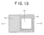
- FIG. 13 is a view showing a conductor pattern arranged on a lower side surface of a lower dielectric substrate shown in FIG. 9 .
- the cross sectional view shown in FIG. 9 is given in the form of a cross sectional view taken along a line A - A' of FIGS. 10 to 13 .
- ground conductor patterns 2a, 2b, and 2c are arranged on lower sides of dielectric substrates 1a, 1b, and 1c, respectively.
- a strip conductor pattern 3 and a conductor pattern 4 for shorting of a waveguide are arranged on an upper side of the dielectric substrate 1a.
- Vias 5a, 5b, and 5c for a waveguide wall are provided in the dielectric substrates 1a, 1b and, 1c.
- the ground conductor patterns 2a, 2b and, 2c are provided with ground conductor patterns opening portions 6a, 6b and, 6c, respectively.
- the strip conductor pattern 3 is provided on the upper side surface of the dielectric substrate 1a, and the ground conductor pattern 2a is provided in the lower side surface of the dielectric substrate 1a to thereby construct a "microstrip line".
- the conductor pattern 4 for shorting of a waveguide is provided in the upper side surface of the dielectric substrate 1a
- the ground conductor pattern 2a is provided on the lower side surface of the dielectric substrate 1a
- the vias 5a for a waveguide wall for connecting the conductor pattern 4 for shorting of a waveguide and the ground conductor pattern 2a to each other are provided to thereby construct a "waveguide shorting portion".
- the ground conductor pattern 2b is provided on the lower side surface of the dielectric substrate 1b, and the vias 5b for a waveguide wall for connecting the ground conductor patterns 2a and 2b to each other are provided to thereby construct a "dielectric waveguide" (first dielectric waveguide).
- the ground conductor pattern 2c is provided on the lower side surface of the dielectric substrate 1c, and the vias 5c for a waveguide wall for connecting the ground conductor patterns 2b and 2c to each other are provided to thereby construct a "dielectric waveguide” (second dielectric waveguide).
- the waveguide 7 is provided under the dielectric substrate 1c so as to correspond to an opening of the dielectric waveguide.
- a high frequency signal inputted to the microstrip line provided on the dielectric substrate 1a is propagated through the dielectric waveguide formed using the dielectric substrate 1b via the waveguide shorting portion. Moreover, the high frequency signal passes through the dielectric waveguide formed using the dielectric substrate 1c to be propagated through the waveguide 7 via the ground conductor pattern omission portion 6c.
- Embodiment 3 similarly to Embodiment 1, the shorting waveguide block projecting from the dielectric substrate by about 1/4 of the guide wavelength as in the above-mentioned prior art example is removed and the highly accurate assembly is not required. Hence, it is possible to realize the miniature waveguide-to-microstrip transition which is easy in mass production.
- the waveguide-to-microstrip transition is constituted by only the conductor patterns and the vias of the substrate.
- the waveguide-to-microstrip transition can be formed inside the dielectric substrate, and can also be incorporated easily in a package formed using ceramics and the like.
- FIG. 14 is a perspective view showing a waveguide-to-microstrip transition according to Embodiment 4 of the present invention.
- a strip conductor pattern width extension portion 8 is provided between a strip conductor pattern 3 and a conductor pattern 4 for shorting of a waveguide.
- the strip conductor pattern width extension portion 8 is provided to thereby allow a shunt capacitance tobe added, it ispossibletocarryoutimpedancematching for a transition having inductance.
- a distribution of the electric field in the microstrip line is concentrated on a dielectric substrate side. Hence, it is possible to suppress the radiation to a space extending above a connection portion between the strip conductor pattern 3 and the conductor pattern 4 for shorting of a waveguide.
- Embodiment 4 similarly to Embodiment 1, the shorting waveguide block projecting from the dielectric substrate by about 1/4 of the guide wavelength as in the above-mentioned prior art example is removed and the highly accurate assembly is not required. Hence, it is possible to realize the miniature waveguide-to-microstrip transition which is easy in mass production.
- the waveguide-to-microstrip transition is constituted by only the conductor patterns and the vias of the substrate.
- the waveguide-to-microstrip transition can be formed inside the dielectric substrate, and can also be incorporated easily in a package formed using ceramics and the like.
- the waveguide-to-microstrip transition has the strip conductor pattern width extension portion 8
- the waveguide-to-microstrip transition can be realized in which the unnecessary radiation from the transition to the space is suppressed. Embodiment 5.
- FIG. 15 is a perspective view showing a waveguide-to-microstrip transition according to Embodiment 5 of the present invention.
- conductor pattern overhang portions 9 for shorting of a waveguide are provided on the both sides of a connection portion between a strip conductor pattern 3 and a conductor pattern 4 for shorting of a waveguide while being apart from the strip conductor pattern 3.
- connection portion between the strip conductor pattern 3 and the conductor pattern 4 for shorting of a waveguide is located above a ground conductor pattern omission portion 6, almost a portion located above the ground conductor pattern omissionportion 6 canbe covered with the conductor pattern. Hence, the radiation to the space extending above the connection portion can be suppressed.
- Embodiment 5 similarly to Embodiment 1, the shorting waveguide block projecting from the dielectric substrate by about 1/4 of the guide wavelength as in the above mentioned prior art example is removed and the highly accurate assembly is not required. Hence, it is possible to realize the miniature waveguide-to-microstrip transition which is easy in mass production.
- the waveguide-to-microstrip transition is constituted by only the conduct or patterns and the vias of the substrate.
- the waveguide-to-microstrip transition can be formed inside the dielectric substrate, and can also be incorporated easily in a package formed using ceramics and the like.
- the waveguide-to-microstrip transition has the conductor pattern over-hang portions 9 for shorting of a waveguide, there is also offered an effect that the unnecessary radiation from the transition to the space can be suppressed.
- the present invention concerns a waveguide-microstrip transition, comprising:
- the present invention concerns a waveguide-to-microstrip transition, comprising:
- the present invention concerns a waveguide-to-microstrip transition, comprising:
- an area surrounded by the second connecting conductors within the second dielectric substrate may be different in size from an area surrounded by the third connecting conductors within the third dielectric substrate.
- a strip conductor pattern width extension portion may be inserted between the strip conductor pattern and the conductor pattern for shorting of a waveguide.
- a cutout portion may be provided in the conductor pattern for shorting of a waveguide.
- the ground conductor pattern omission portion may be a polygon, and a position of a boundary between the strip conductor pattern and the conductor pattern for shorting of a waveguide may agree with one side of the polygon, or may be located inside the polygon.
- the connecting conductors may be constituted by a plurality of vias.
- the shorting waveguide block projecting from the dielectric substrate by about 1/4 of a guide wavelength has in the prior art example is removed, and hence highly accurate assembly is not also required, the miniature waveguide-to-microstrip transition is obtained which is easy in mass production.
- the waveguide-to-microstrip transition is constituted by only the conductor patterns and the vias of the substrate, the waveguide-to-microstrip transition can be formed inside the dielectric substrate, and can also be incorporated easily in a package formed using ceramics and the like.
Landscapes
- Waveguides (AREA)
Abstract
Description
- The present invention relates to a waveguide-to-microstrip transition mainly used in a microwave band and a millimeter-wave band.
- In a conventional waveguide-to-microstrip transition, a dielectric substrate is fixed so as to be held between a waveguide and a shorting waveguide block. Astripconductorpatternisprovided on one surface of the dielectric substrate, and a ground conductor pattern connected to an opening portion of the waveguide is provided on the other surface of the dielectric substrate. The strip conductor pattern, the ground conductor pattern, and the dielectric substrate constitute a microstrip line. If a distance between a shorting surface of the shorting waveguide block and the strip conductor pattern is set to about 1/4 of a guide wavelength of the waveguide, then a magnitude of a magnetic field within the waveguide becomes maximum in a position where the strip conductor pattern is inserted. Hence, a propagation mode of the microstrip line and a propagation mode of the waveguide are well coupled to each other. Accordingly, a high frequency signal which has been propagated through the waveguide can be propagated through the microstrip line without generating a large reflection (for example, refer to
JP 2000-244212 A FIG. 13 )). - In such a conventional waveguide-to-microstrip transition as described above, about 1/4 of the guide wavelength of the waveguide is required for a length from the strip conductor pattern to the shorting surface of the shorting waveguide block. Hence, the shorting waveguide block is proj ected from the dielectric substrate. Accordingly, there is a problem in that a transition is difficult to be miniaturized especially in a microwave band.
- On the other hand, if aposition shift occurs among the waveguide, then the shorting waveguide block, and the strip conductor pattern, characteristics of the transition are degraded. Thus, it is necessary to assemble the components or parts with high accuracy. However, there is a problem in that since the components or parts need to be made very small in the millimeter-wave band, the components or parts are difficult to be assembled with high accuracy, and hence mass production of the transition is difficult to be realized.
- In addition, in the case where the conventional waveguide-to-microstrip transition is provided in an input/output portion of a package having high frequency elements mounted thereto, a space is made in a connection portion between the waveguide and the microstrip line. Thus, there is also a problem in that the inside of the package can not be hermetically sealed.
- The present invention has been made in order to solve the above-mentioned problems, and it is therefore an object of the present invention to obtain a miniature waveguide-to-microstrip transition which is easy in mass production in a microwave band and a millimeter-wave band.
- Moreover, it is another object of the present invention to obtain a waveguide-to-microstrip transition in which when the waveguide-to-microstrip transition is applied to a high frequency package having a waveguide connected at an input/output portion, the inside of the package can be hermetically sealed.
- Awaveguide-to-microstrip transition according to the present invention includes: a dielectric substrate; a ground conductor pattern which is formed on one surface of the dielectric substrate and which has a ground conductor pattern omission portion; a strip conductor pattern formed on a surface of the dielectric substrate opposite to the surface having the ground conductor pattern; a conductor pattern for shorting of a waveguide formed so as to be continuously connected to the strip conductor pattern; connecting conductors for connecting the ground conductor pattern and the conductor pattern for shorting of a waveguide to each other within the dielectric substrate; and a waveguide connected to the dielectric substrate so as to correspond to the ground conductor pattern omission portion.
- Also, a microstrip line is constituted by the strip conductor pattern, the ground conductor pattern, and the dielectric substrate.
- Further, a dielectric waveguide shorting portion is constituted by the conductor pattern for shorting of a waveguide, the ground conductor pattern, and the connecting conductors.
-
-
FIG. 1 is a perspective view showing a construction of a waveguide-to-microstrip transition according to Embodiment 1 of the present invention; -
FIG. 2 is a cross sectional view showing a construction of the waveguide-to-microstrip transition according to Embodiment 1 of the present invention; -
FIG. 3 is a view showing a conductor pattern arranged on an upper side surface of a dielectric substrate shown inFIG. 1 ; -
FIG. 4 is a view showing a conductor pattern arranged on a lower side surface of the dielectric substrate shown inFIG. 1 ; -
FIG. 5 is a cross sectional view showing a construction of a waveguide-to-microstrip transition according toEmbodiment 2 of the present invention; -
FIG. 6 is a view showing a conductor pattern arranged on an upper side surface of an upper dielectric substrate shown inFIG. 5 ; -
FIG. 7 is a view showing a conductor pattern arranged on a lower side surface of the upper dielectric substrate shown inFIG. 5 ; -
FIG. 8 is a view showing a conductor pattern arranged on a lower side surface of a lower dielectric substrate shown inFIG. 5 ; -
FIG. 9 is a cross sectional view showing a construction of a waveguide-to-microstrip transition according toEmbodiment 3 of the present invention; -
FIG. 10 is a view showing a conductor pattern arranged on an upper side surface of an upper dielectric substrate shown inFIG. 9 ; -
FIG. 11 is a view showing a conductor pattern arranged on a lower side surface of the upper dielectric substrate shown inFIG. 9 ; -
FIG. 12 is a view showing a conductor pattern arranged on a lower side surface of a middle dielectric substrate shown inFIG. 9 ; -
FIG. 13 is a view showing a conductor pattern arranged on a lower side surface of a lower dielectric substrate shown inFIG. 9 ; -
FIG. 14 is a perspective view showing a construction of a waveguide-to-microstrip transition according toEmbodiment 4 of the present invention; and -
FIG. 15 is a perspective view showing a construction of a waveguide-to-microstrip transition according toEmbodiment 5 of the present invention. - Embodiments of the present invention will hereinafter be described on the basis of the drawings.
- A waveguide-to-microstrip transition according to Embodiment 1 of the present invention will now be described with reference to the drawings.
FIG. 1 is a perspective view showing a construction of a waveguide-to-microstrip transition according to Embodiment 1 of the present invention. -
FIG. 2 is a cross sectional view showing the waveguide-to-microstrip transition shown inFig. 1 . Also,FIG. 3 is a view showing a conductor pattern arranged on an upper side surface of a dielectric substrate shown inFIG. 1 . Moreover,FIG. 4 is a view showing a conductor pattern arranged on a lower side surface of the dielectric substrate shown inFIG. 1 . Note that the cross sectional view shown inFIG. 2 is given in the form of a cross sectional view taken along a lineA-A' ofFIGS. 3 and 4 . In addition, in those figures, the same reference numerals designate the same or corresponding portions. - In
FIGS. 1 to 4 , aground conductor pattern 2 is arranged on a lower side surface of a dielectric substrate 1. Astrip conductor pattern 3 and aconductor pattern 4 for shorting of a waveguide are arranged on an upper side surface of the dielectric substrate 1.Vias 5 for a waveguide wall (conductors for connection) are provided across theground conductor pattern 2 and theconductor pattern 4 for shorting of a waveguide. In addition, a ground conductorpattern omission portion 6 is provided in theground conductor pattern 2. Awaveguide 7 is provided on a lower side of theground conductor pattern 2. Note that the via is used as a term meaning a columnar conductor in this specification. - In addition, in those figures, the
ground conductor pattern 2, thestrip conductor pattern 3, and the dielectric substrate 1 constitute "a microstrip line". Thevias 5 for a waveguide wall are provided in the periphery of the ground conductorpattern omission portion 6 in order to connect theground conductor pattern 2 and theconductor pattern 4 for shorting of a waveguide to each other. Theground conductor pattern 2, theconductor pattern 4 for shorting of a waveguide, and thevias 5 for a waveguide wall constitute a "dielectric waveguide shorting portion". Thewaveguide 7 is connected so as to correspond to the ground conductorpattern omission portion 6 provided on the lower side of the dielectric substrate 1. - Next, an operation of the waveguide-to-microstrip transition according to Embodiment 1 will hereinbelow be described with reference to the drawings.
- In the microstrip line, an electric field is generated between the
ground conductor pattern 2 and thestrip conductor pattern 3. On the other hand, in thewaveguide 7, a central portion of the waveguide cross section has a distribution of the strongest electric field. Then, if thestrip conductor pattern 3 constituting the microstrip line is connected to a center of the dielectric waveguide shorting portion of theconductor pattern 4 for shorting of a waveguide constituting the dielectric waveguide shorting portion, then a portion having the generated electric field in the microstrip line agrees with a portion having a strong electric field in thewaveguide 7. Since the electric field distribution of the microstrip line is near that of thewaveguide 7, a high frequency signal can be propagated without generating a large reflection. - As described above, according to Embodiment 1, the shorting waveguide block projecting from the dielectric substrate by about 1/4 of the guide wavelength as in the above-mentioned prior art example is removed and the highly accurate assembly is not required. Hence, there is offered an effect that the miniature waveguide-to-microstrip transition is realized which is easy in mass production.
- In addition, the waveguide-to-microstrip transition is constituted by only the conductor patterns and the vias of the substrate. Thus, there is also offered an effect that the waveguide-to-microstrip transition can be formed inside the dielectric substrate, and can also be incorporated easily in a package formed using ceramics and the like.
- Next, a waveguide-to-microstrip transition according to
Embodiment 2 of the present invention will hereinbelow be described with reference to the drawings. -
FIG. 5 is a cross sectional view showing a construction of the waveguide-to-microstrip transition according toEmbodiment 2 of the present invention. Also,FIG. 6 is a view showing a conductor pattern arranged on an upper side surface of an upper dielectric substrate shown inFIG. 5 .FIG. 7 is a view showing a conductor pattern arranged on a lower side surface of the upper dielectric substrate shown inFIG. 5 . Moreover,FIG. 8 is a view showing a conductor pattern arranged on a lower side surface of a lower dielectric substrate shown inFIG. 5 . Note that, the cross sectional view shown inFIG. 5 is given in the form of a cross sectional view taken along a line A - A' ofFIGS. 6 to 8 . - In
FIGS. 5 to 8 , aground conductor pattern 2a is arranged on a lower side surface of a dielectric substrate 1a. Aground conductor pattern 2b is arranged on a lower side surface of a dielectric substrate 1b. Astrip conductor pattern 3 and aconductor pattern 4 for shorting of a waveguide are arranged on an upper side surface of the dielectric substrate 1a. Vias 5a for a waveguide wall are provided across theground conductor pattern 2a and theconductor pattern 4 for shorting of a waveguide. Vias 5b for a waveguide wall are provided across theground conductor pattern 2b and theground conductor pattern 2a. In addition, a ground conductorpattern omission portion 6a is provided in theground conductor pattern 2a. A ground conductorpattern omission portion 6b is provided in theground conductor pattern 2b. Awaveguide 7 is provided on a lower side of theground conductor pattern 2b. - The
strip conductor pattern 3 is provided on the upper side surface of the dielectric substrate 1a, and theground conductor pattern 2a is provided in the lower side surface of the dielectric substrate 1a to thereby construct a "microstripline". In addition, theconductor pattern 4 for shorting of a waveguide is provided in the upper side surface of the dielectric substrate 1a, theground conductor pattern 2a is provided on the lower side surface of the dielectric substrate 1a, and thevias 5a for a waveguide wall for connecting theconductor pattern 4 for shorting of a waveguide and theground conductor pattern 2a to each other are provided to thereby construct a "waveguide shorting portion". Moreover, theground conductor pattern 2b is provided on the lower side surface of the dielectric substrate 1b, and thevias 5b for a waveguide wall for connecting theground conductor patterns waveguide 7 is provided under the dielectric substrate 1b so as to correspond to an opening of the dielectric waveguide. - Next, an operation of the waveguide-to-microstrip transition according to
Embodiment 2 will hereinbelow be described with reference to the drawings. - In the waveguide-to-microstrip transition having the construction as described above, a high frequency signal inputted to the microstrip line provided on the dielectric substrate 1a is propagated through the dielectric waveguide formed using the dielectric substrate 1b via the waveguide shorting portion. Moreover, the high frequency signal passes through the ground conductor
pattern omission portion 6b to be propagated through thewaveguide 7. - As described above, according to
Embodiment 2, similarly to the above-mentioned embodiment 1, the shorting waveguide block projecting from the dielectric substrate by about 1/4 of the guide wavelength as in the above-mentioned prior art example is removed and the highly accurate assembly is not required. Hence, it is possible to realize the miniature waveguide-to-microstrip transition which is easy in mass production. - In addition, the waveguide-to-microstrip transition is constituted by only the conductor patterns and the vias of the substrate. Thus, there is offered an effect that the waveguide-to-microstrip transition can be formed inside the dielectric substrate, and can also be incorporated easily in a package formed using ceramics and the like.
- Moreover, an impedance of the dielectric waveguide which is constituted by the ground conductor pattern, and the vias for a waveguide wall within the dielectric substrate is adjusted, whereby it is possible to realize the waveguide-to-microstrip transition which has the excellent characteristics and with which impedance matching with a waveguide connected to the outside is easy to be obtained.
- Next, a waveguide-to-microstrip transition according to
Embodiment 3 of the present invention will hereinbelow be described with reference to the drawings. -
FIG. 9 is a cross sectional view showing a construction of the waveguide-to-microstrip transition according toEmbodiment 3 of the present invention. Also,FIG. 10 is a view showing a conductor pattern arranged on an upper side surface of an upper dielectric substrate shown inFIG. 9 .FIG. 11 is a view showing a conductor pattern arranged on a lower side surface of the upper dielectric substrate shown inFIG. 9 . Moreover,FIG. 12 is a view showing a conductor pattern arranged on a lower side surface of a middle dielectric substrate shown inFIG. 9 .FIG. 13 is a view showing a conductor pattern arranged on a lower side surface of a lower dielectric substrate shown inFIG. 9 . Note that, the cross sectional view shown inFIG. 9 is given in the form of a cross sectional view taken along a line A - A' ofFIGS. 10 to 13 . - In
FIGS. 9 to 13 ,ground conductor patterns strip conductor pattern 3 and aconductor pattern 4 for shorting of a waveguide are arranged on an upper side of the dielectric substrate 1a. Vias 5a, 5b, and 5c for a waveguide wall are provided in the dielectric substrates 1a, 1b and, 1c. In addition, theground conductor patterns patterns opening portions - The
strip conductor pattern 3 is provided on the upper side surface of the dielectric substrate 1a, and theground conductor pattern 2a is provided in the lower side surface of the dielectric substrate 1a to thereby construct a "microstrip line". In addition, theconductor pattern 4 for shorting of a waveguide is provided in the upper side surface of the dielectric substrate 1a, theground conductor pattern 2a is provided on the lower side surface of the dielectric substrate 1a, and thevias 5a for a waveguide wall for connecting theconductor pattern 4 for shorting of a waveguide and theground conductor pattern 2a to each other are provided to thereby construct a "waveguide shorting portion". Moreover, theground conductor pattern 2b is provided on the lower side surface of the dielectric substrate 1b, and thevias 5b for a waveguide wall for connecting theground conductor patterns ground conductor pattern 2c is provided on the lower side surface of the dielectric substrate 1c, and thevias 5c for a waveguide wall for connecting theground conductor patterns waveguide 7 is provided under the dielectric substrate 1c so as to correspond to an opening of the dielectric waveguide. - Next, an operation of the waveguide-to-microstrip transition according to
Embodiment 3 will hereinbelow be described with reference to the drawings. - In the waveguide-to-microstrip transition having the construction as described above, a high frequency signal inputted to the microstrip line provided on the dielectric substrate 1a is propagated through the dielectric waveguide formed using the dielectric substrate 1b via the waveguide shorting portion. Moreover, the high frequency signal passes through the dielectric waveguide formed using the dielectric substrate 1c to be propagated through the
waveguide 7 via the ground conductorpattern omission portion 6c. - As described above, according to
Embodiment 3, similarly to Embodiment 1, the shorting waveguide block projecting from the dielectric substrate by about 1/4 of the guide wavelength as in the above-mentioned prior art example is removed and the highly accurate assembly is not required. Hence, it is possible to realize the miniature waveguide-to-microstrip transition which is easy in mass production. - In addition, the waveguide-to-microstrip transition is constituted by only the conductor patterns and the vias of the substrate. Thus, there is also offered an effect that the waveguide-to-microstrip transition can be formed inside the dielectric substrate, and can also be incorporated easily in a package formed using ceramics and the like.
- Moreover, since a plurality of dielectric waveguides formed using the ground conductor patterns and the vias for a waveguide wall within the dielectric substrates are operated as a multisection impedance transformer, it becomes possible to obtain the impedance matching over a broad band.
- A waveguide-to-microstrip transition according to
Embodiment 4 of the present invention will hereinbelow be described with reference to the drawings. -
FIG. 14 is a perspective view showing a waveguide-to-microstrip transition according toEmbodiment 4 of the present invention. InFIG. 14 , a strip conductor pattern width extension portion 8 is provided between astrip conductor pattern 3 and aconductor pattern 4 for shorting of a waveguide. - In the waveguide-to-microstrip transition having the construction as described above, since the strip conductor pattern width extension portion 8 is provided to thereby allow a shunt capacitance tobe added, it ispossibletocarryoutimpedancematching for a transition having inductance. In addition, in the strip conductor pattern width extension portion 8, a distribution of the electric field in the microstrip line is concentrated on a dielectric substrate side. Hence, it is possible to suppress the radiation to a space extending above a connection portion between the
strip conductor pattern 3 and theconductor pattern 4 for shorting of a waveguide. - As described above, according to
Embodiment 4, similarly to Embodiment 1, the shorting waveguide block projecting from the dielectric substrate by about 1/4 of the guide wavelength as in the above-mentioned prior art example is removed and the highly accurate assembly is not required. Hence, it is possible to realize the miniature waveguide-to-microstrip transition which is easy in mass production. - In addition, the waveguide-to-microstrip transition is constituted by only the conductor patterns and the vias of the substrate. Thus, there is also offered an effect that the waveguide-to-microstrip transition can be formed inside the dielectric substrate, and can also be incorporated easily in a package formed using ceramics and the like.
- Moreover, since the waveguide-to-microstrip transition has the strip conductor pattern width extension portion 8, the waveguide-to-microstrip transition can be realized in which the unnecessary radiation from the transition to the space is suppressed.
Embodiment 5. - Next, a waveguide-to-microstrip transition according to
Embodiment 5 of the present invention will hereinbelow be described with reference to the drawings. -
FIG. 15 is a perspective view showing a waveguide-to-microstrip transition according toEmbodiment 5 of the present invention. InFIG. 15 , conductor pattern overhang portions 9 for shorting of a waveguide are provided on the both sides of a connection portion between astrip conductor pattern 3 and aconductor pattern 4 for shorting of a waveguide while being apart from thestrip conductor pattern 3. - In the waveguide-to-microstrip transition having the construction as described above, even when the connection portion between the
strip conductor pattern 3 and theconductor pattern 4 for shorting of a waveguide is located above a ground conductorpattern omission portion 6, almost a portion located above the groundconductor pattern omissionportion 6 canbe covered with the conductor pattern. Hence, the radiation to the space extending above the connection portion can be suppressed. - As described above, according to
Embodiment 5, similarly to Embodiment 1, the shorting waveguide block projecting from the dielectric substrate by about 1/4 of the guide wavelength as in the above mentioned prior art example is removed and the highly accurate assembly is not required. Hence, it is possible to realize the miniature waveguide-to-microstrip transition which is easy in mass production. - In addition, the waveguide-to-microstrip transition is constituted by only the conduct or patterns and the vias of the substrate. Thus, there is also offered an effect that the waveguide-to-microstrip transition can be formed inside the dielectric substrate, and can also be incorporated easily in a package formed using ceramics and the like.
- Moreover, since the waveguide-to-microstrip transition has the conductor pattern over-hang portions 9 for shorting of a waveguide, there is also offered an effect that the unnecessary radiation from the transition to the space can be suppressed.
- In a first further aspect, the present invention concerns a waveguide-microstrip transition, comprising:
- a dielectric substrate; a ground conductor pattern which is formed on one surface of the dielectric substrate and which has a ground conductor pattern omission portion; a strip conductor pattern formed on a surface of the dielectric substrate opposite to the surface having the ground conductor pattern; a conductor pattern for shorting of a waveguide formed so as to be continuously connected to the strip conductor pattern; connecting conductors for connecting the ground conductor pattern and the conductor pattern for shorting of a waveguide to each other within the dielectric substrate; and a waveguide connected to the dielectric substrate so as to correspond to the ground conductor pattern omission portion,
- wherein a microstrip line is constituted by the strip conductor pattern, the ground conductor pattern, and the dielectric substrate, and
- a dielectric waveguide shorting portion is constituted by the conductor pattern for shorting of a waveguide, the ground conductor pattern, and the connecting conductors.
- In a second further aspect, the present invention concerns a waveguide-to-microstrip transition, comprising:
- a first dielectric substrate; a first ground conductor pattern which is formed on one surface of the first dielectric substrate and which has a first ground conductor pattern omission portion; a strip conductor pattern formed on a surface of the first dielectric substrate opposite to the surface having the first ground conductor pattern; a conductor pattern for shorting of a waveguide formed so as to be continuously connected to the strip conductor pattern; and first connecting conductors for connecting the first ground conductor pattern and the conductor pattern which is formed on one surface of the second dielectric substrate and which has a second ground conductor pattern omission portion; second connecting conductors provided in a periphery of the second ground conductor pattern omission portion so as to vertically extend through the second dielectric substrate; and a waveguide connected to the second dielectric substrate so as to correspond to the second ground conductor pattern omission portion,
- wherein the first dielectric substrate and the second dielectric substrate are laminated so that the first ground conductor pattern faces a surface of the second dielectric substrate opposite to the surface having the second ground conductor pattern,
- a microstrip line is constituted by the strip conductor pattern, the first ground conductor pattern, and the first dielectric substrate,
- a waveguide shorting portion is constituted by the conductor pattern for shorting of a waveguide, the first ground conductor patterns, and the first connecting conductors, and
- a dielectric waveguide is constituted by the first ground conductor patterns, the second ground conductor pattern, and the second connecting conductors.
- In a third further aspect, the present invention concerns a waveguide-to-microstrip transition, comprising:
- A first dielectric substrate; a first ground conductor pattern which is formed on one surface of the first dielectric substrate and which has a frist ground conductor pattern omission portion; a strip conductor pattern formed on a surface of the first dielectric substrate opposite to the surface having the first ground conductor pattern; a conductor pattern for shorting of a waveguide formed so as to be continuously connected to the strip conductor pattern; and first connecting conductors for connecting the first ground conductor pattern and the conductor pattern for shorting of a waveguide to each other within the first dielectric substrate;
- a second dielectric substrate; a second ground conductor pattern which is formed on the surface of the second dielectric substrate and which has a second ground conductor pattern omission portion; and second connecting conductors provided in a periphery of the second ground conductor pattern omission portion so as to vertically extend through the second dielectric substrate; and
- a third dielectric substrate; a third ground conductor pattern which is formed on one surface of the third dielectric substrate and which has a third ground conductor pattern omission portion; third connecting conductors provided in a periphery of the third ground conductor pattern omission portion so as to verticafly extend through the third dielectric substrate; and a waveguide connected to the third dielectric substrate so as to correspond to the third ground conductor pattern omission portion,
- wherein the first dielectric substrate and the second dielectric substrate are laminated so that the first ground conductor pattern faces a surface of the second dielectric substrate opposite to the surface having the second dielectric substrate opposite to the surface having the second ground conductor pattern,
- the second dielectric substrate and the third dielectric substrate are laminated so that the second ground conductor pattern faces a surface of the third dielectric substrate opposite to the surface having the third ground conductor pattern,
- a microstrip line is constituted by the strip conductor pattern, the first ground conductor pattern, and the first dielectric substrate,
- a waveguide shorting portion is constituted by the conductor pattern for shorting of a waveguide, the first ground conductor pattern, and the first connecting conductors,
- a first dielectric waveguide is constituted by the first ground conductor pattern, the second ground conductor pattern, and the second connecting conductors, and
- a second dielectric waveguide is constituted by the second ground conductor pattern, the third ground conductor pattern, and the third connecting conductors.
- In the waveguide-to-microstrip transition according to the previous third further aspect an area surrounded by the second connecting conductors within the second dielectric substrate may be different in size from an area surrounded by the third connecting conductors within the third dielectric substrate.
- In a waveguide-to-microstrip transition according to the first further aspect a strip conductor pattern width extension portion may be inserted between the strip conductor pattern and the conductor pattern for shorting of a waveguide.
- In a waveguide-to-microstrip transition according to the first further aspect a cutout portion may be provided in the conductor pattern for shorting of a waveguide.
- In a waveguide-to-microstrip transition according to the first further aspect, the ground conductor pattern omission portion may be a polygon, and a position of a boundary between the strip conductor pattern and the conductor pattern for shorting of a waveguide may agree with one side of the polygon, or may be located inside the polygon.
- In a waveguide-to-microstrip transition according to the first further aspect the connecting conductors may be constituted by a plurality of vias.
- According to the present invention, as described above, since the shorting waveguide block projecting from the dielectric substrate by about 1/4 of a guide wavelength has in the prior art example is removed, and hence highly accurate assembly is not also required, the miniature waveguide-to-microstrip transition is obtained which is easy in mass production.
- In addition, since the waveguide-to-microstrip transition is constituted by only the conductor patterns and the vias of the substrate, the waveguide-to-microstrip transition can be formed inside the dielectric substrate, and can also be incorporated easily in a package formed using ceramics and the like.
Claims (2)
- A waveguide-microstrip line transition, comprising:a first dielectric substrate (1a); a first ground conductor pattern (2a) which is formed on one surface of the first dielectric substrate (1a) and which has a first ground conductor pattern omission portion (6a); a strip conductor pattern (3) formed on a surface of the first dielectric substrate (1a) opposite to the surface having the first ground conductor pattern (2a); a conductor pattern (4) for shorting of a waveguide formed so as to be continuously connected to the strip conductor pattern (3); and first connecting conductors (5a) for connecting the first ground conductor pattern (2a) andthe conductor pattern (4) for shorting of a waveguide to each other within the first dielectric substrate (1a);a second dielectric substrate (1b); a second ground conductor pattern (2b) which is formed on the surface of the second dielectric substrate (1b) andwhich has a second ground conductor pattern omission portion (6b); andsecond connecting conductors (5b) provided in a periphery of the second ground conductor pattern omission portion (6b) so as to vertically extend through the second dielectric substrate (1b); anda third dielectric substrate (1c); a third ground conductor pattern (2c) which is formed on one surface of the third dielectric substrate (1c) andwhich has a third ground conductor pattern omission portion (6c); third connecting conductors (5c) provided in a periphery of the third ground conductor pattern omission portion (6c) so as to vertically extend through the third dielectric substrate (1c); anda waveguide (7) connected to the third dielectric substrate (1c) so as to correspond to the third ground conductor pattern omission portion (6c),wherein the first dielectric substrate (1a) and the second dielectric substrate (1b) are laminated so that the first ground conductor pattern (2a) faces a surface of the second dielectric substrate (1b) opposite to the surface having the second ground conductor pattern (2b),wherein the second dielectric substrate (1b) and the third dielectric substrate (1c) are laminated so that the second ground conductor pattern (2b) faces a surface of the third dielectric substrate (1c) opposite to the surface having the third ground conductor pattern (2c),wherein a microstrip line is constituted by the strip conductor pattern (3), the first ground conductor pattern (2a), and the first dielectric substrate (1a),wherein a waveguide shorting portion is constituted by the conductor pattern (4) for shorting of a waveguide, the first ground conductor pattern (2a), and the first connecting conductors (5a),wherein a first dielectric waveguide is constituted by the first ground conductor pattern (2a), the second ground conductor pattern (2b), and the second connecting conductors (5b),wherein a second dielectric waveguide is constituted by the second ground conductor pattern (2b), the third ground conductor pattern (2c), and the third connecting conductors (5c), andwherein an area surrounded by the second connecting conductors (5b) within the second dielectric substrate (1b) is different in size from an area surrounded by the third connecting conductors (5c) within the third dielectric substrate (1c),wherein the first dielectric waveguide is disposed on the second dielectric substrate (1b),wherein the second dielectric waveguide is disposed on the third dielectric substrate (1c),wherein the ground conductor pattern omission portion (6a, 6b, 6c) is arrayed to face the bottom of the conductor pattern (4) for shorting of a waveguide connected to the strip conductor pattern (3).
- A waveguide-microstrip line transition, comprising:a first dielectric substrate (1a); a first ground conductor pattern (2a) which is formed on one surface of the first dielectric substrate (1a) and which has a first ground conductor pattern omission portion (6a); a strip conductor pattern (3) formed on a surface of the first dielectric substrate (1a) opposite to the surface having the first ground conductor pattern (2a); a conductor pattern (4) for shorting of a waveguide formed so as to be continuously connected to the strip conductor pattern (3); and first connecting conductors (5a) for connecting the first ground conductor pattern (2a) and the conductor pattern (4) for shorting of a waveguide to each other within the first dielectric substrate (1a);a second dielectric substrate (1b); a second ground conductor pattern (2b) which is formed on the surface of the second dielectric substrate (1b) and which has a second ground conductor pattern omission portion (6b); and second connecting conductors (5b) provided in a periphery of the second ground conductor pattern omission portion (6b) so as to vertically extend through the second dielectric substrate (1b); anda third dielectric substrate (1c); a third ground conductor pattern (2c) which is formed on one surface of the third dielectric substrate (1c) and which has a third ground conductor pattern omission portion (6c); third connecting conductors (5c) provided in a periphery of the third ground conductor pattern omission portion (6c) so as to vertically extend through the third dielectric substrate (1c); anda waveguide (7) connected to the third dielectric substrate (1c) so as to correspond to the third ground conductor pattern omission portion (6c),wherein the first dielectric substrate (1a) and the second dielectric substrate (1b) are laminated so that the first ground conductor pattern (2a) faces a surface of the second dielectric substrate (1b) opposite to the surface having the second ground conductor pattern (2b),wherein the second dielectric substrate (1b) and the third dielectric substrate (1c) are laminated so that the second ground conductor pattern (2b) faces a surface of the third dielectric substrate (1c) opposite to the surface having the third ground conductor pattern (2c),wherein a microstrip line is constituted by the strip conductor pattern (3), the first ground conductor pattern (2a), and the first dielectric substrate (1a),wherein a waveguide shorting portion is constituted by the conductor pattern (4) for shorting of a waveguide, the first ground conductor pattern (2a), and the first connecting conductors (5a),wherein a first dielectric waveguide is constituted by the first ground conductor pattern (2a), the second ground conductor pattern (2b), and the second connecting conductors (5b),wherein a second dielectric waveguide is constituted by the second ground conductor pattern (2b), the third ground conductor pattern (2c), and the third connecting conductors (5c), andwherein an area surrounded by the second connecting conductors (5b) within the second dielectric substrate (1b) is different in size from an area surrounded by the third connecting conductors (5c) within the third dielectric substrate (1c),wherein the first dielectric waveguide is disposed on the second dielectric substrate (1b),wherein the second dielectric waveguide is disposed on the third dielectric substrate (1c),wherein a high frequency signal inputted to the microstrip line provided on the dielectric substrate (1a) is propagated through the dielectric waveguide formed using the dielectric substrate (1b) via the waveguide shorting portion, and the high frequency signal passes through the dielectric waveguide formed using the dielectric substrate (1c) to be propagated through the waveguide (7) via the ground conductor pattern omission portion (6c).
Applications Claiming Priority (3)
| Application Number | Priority Date | Filing Date | Title |
|---|---|---|---|
| JP2002068754A JP3828438B2 (en) | 2002-03-13 | 2002-03-13 | Waveguide / microstrip line converter |
| PCT/JP2003/002927 WO2003077353A1 (en) | 2002-03-13 | 2003-03-12 | Waveguide/microstrip line converter |
| EP03710321.5A EP1396902B1 (en) | 2002-03-13 | 2003-03-12 | Waveguide/microstrip line converter |
Related Parent Applications (2)
| Application Number | Title | Priority Date | Filing Date |
|---|---|---|---|
| EP03710321.5A Division EP1396902B1 (en) | 2002-03-13 | 2003-03-12 | Waveguide/microstrip line converter |
| EP03710321.5A Division-Into EP1396902B1 (en) | 2002-03-13 | 2003-03-12 | Waveguide/microstrip line converter |
Publications (2)
| Publication Number | Publication Date |
|---|---|
| EP2905839A1 true EP2905839A1 (en) | 2015-08-12 |
| EP2905839B1 EP2905839B1 (en) | 2019-09-04 |
Family
ID=27800309
Family Applications (2)
| Application Number | Title | Priority Date | Filing Date |
|---|---|---|---|
| EP15154475.6A Expired - Lifetime EP2905839B1 (en) | 2002-03-13 | 2003-03-12 | Waveguide-to-microstrip transition |
| EP03710321.5A Expired - Lifetime EP1396902B1 (en) | 2002-03-13 | 2003-03-12 | Waveguide/microstrip line converter |
Family Applications After (1)
| Application Number | Title | Priority Date | Filing Date |
|---|---|---|---|
| EP03710321.5A Expired - Lifetime EP1396902B1 (en) | 2002-03-13 | 2003-03-12 | Waveguide/microstrip line converter |
Country Status (4)
| Country | Link |
|---|---|
| US (2) | US7148765B2 (en) |
| EP (2) | EP2905839B1 (en) |
| JP (1) | JP3828438B2 (en) |
| WO (1) | WO2003077353A1 (en) |
Families Citing this family (35)
| Publication number | Priority date | Publication date | Assignee | Title |
|---|---|---|---|---|
| WO2005083832A1 (en) | 2004-02-27 | 2005-09-09 | Mitsubishi Denki Kabushiki Kaisha | Transducer circuit |
| JP4158745B2 (en) | 2004-06-18 | 2008-10-01 | 株式会社デンソー | Waveguide / transmission line converter |
| JP4867359B2 (en) * | 2005-07-06 | 2012-02-01 | 日立化成工業株式会社 | Transmission line interlayer connection structure |
| KR100714451B1 (en) | 2005-12-08 | 2007-05-04 | 한국전자통신연구원 | Dielectric Waveguide vs. Standard Waveguide Transition |
| JP4568235B2 (en) * | 2006-02-08 | 2010-10-27 | 株式会社デンソー | Transmission line converter |
| JP4622954B2 (en) * | 2006-08-01 | 2011-02-02 | 株式会社デンソー | Line waveguide converter and wireless communication device |
| JP2009545904A (en) * | 2006-08-04 | 2009-12-24 | エイアールエム リミテッド | Bus interconnect device and data processing apparatus including said bus interconnect device |
| KR100846872B1 (en) | 2006-11-17 | 2008-07-16 | 한국전자통신연구원 | Apparatus for the transition of dielectric waveguide and transmission line in millimeter wave band |
| JP4365852B2 (en) | 2006-11-30 | 2009-11-18 | 株式会社日立製作所 | Waveguide structure |
| JP4648292B2 (en) * | 2006-11-30 | 2011-03-09 | 日立オートモティブシステムズ株式会社 | Millimeter-wave transceiver and in-vehicle radar using the same |
| JP2008193161A (en) * | 2007-01-31 | 2008-08-21 | Hitachi Kokusai Electric Inc | Microstrip line-waveguide converter |
| JP4975100B2 (en) | 2007-04-25 | 2012-07-11 | 三菱電機株式会社 | Even harmonic mixer |
| JP4827799B2 (en) * | 2007-06-18 | 2011-11-30 | 三菱電機株式会社 | Waveguide / microstrip line converter |
| US7609223B2 (en) * | 2007-12-13 | 2009-10-27 | Sierra Nevada Corporation | Electronically-controlled monolithic array antenna |
| US8059051B2 (en) | 2008-07-07 | 2011-11-15 | Sierra Nevada Corporation | Planar dielectric waveguide with metal grid for antenna applications |
| JP2010056920A (en) * | 2008-08-28 | 2010-03-11 | Mitsubishi Electric Corp | Waveguide microstrip line converter |
| JP5289551B2 (en) * | 2009-02-27 | 2013-09-11 | 三菱電機株式会社 | Waveguide microstrip line converter |
| JP5377070B2 (en) * | 2009-05-14 | 2013-12-25 | 三菱電機株式会社 | Waveguide / microstrip line converter |
| JP5476873B2 (en) | 2009-09-05 | 2014-04-23 | 富士通株式会社 | Signal converter and manufacturing method thereof |
| EP2618421A1 (en) * | 2012-01-19 | 2013-07-24 | Huawei Technologies Co., Ltd. | Surface Mount Microwave System |
| US20150123862A1 (en) * | 2013-11-07 | 2015-05-07 | Thinkom Solutions, Inc. | Waveguide to parallel-plate transition and device including the same |
| JP2015149649A (en) * | 2014-02-07 | 2015-08-20 | 株式会社東芝 | Millimeter-wave band semiconductor package and millimeter-wave band semiconductor device |
| JP2015149650A (en) * | 2014-02-07 | 2015-08-20 | 株式会社東芝 | Millimeter-wave band semiconductor package and millimeter-wave band semiconductor device |
| JP6239477B2 (en) * | 2014-09-26 | 2017-11-29 | 古河電気工業株式会社 | Planar transmission line / waveguide converter |
| JP2016072881A (en) * | 2014-09-30 | 2016-05-09 | 日本電産エレシス株式会社 | High frequency power conversion mechanism |
| KR101621480B1 (en) * | 2014-10-16 | 2016-05-16 | 현대모비스 주식회사 | Transit structure of waveguide and dielectric waveguide |
| JP6313812B2 (en) * | 2016-06-13 | 2018-04-18 | 株式会社フジクラ | Power supply device |
| JP6313813B2 (en) * | 2016-06-13 | 2018-04-18 | 株式会社フジクラ | Power supply device |
| WO2019199212A1 (en) * | 2018-04-13 | 2019-10-17 | Saab Ab | Waveguide launch |
| US10811752B2 (en) * | 2019-03-15 | 2020-10-20 | Thinkom Solutions, Inc. | Offset block waveguide coupler |
| US11658378B2 (en) | 2019-10-14 | 2023-05-23 | International Business Machines Corporation | Vertically transitioning between substrate integrated waveguides (SIWs) within a multilayered printed circuit board (PCB) |
| US11399428B2 (en) | 2019-10-14 | 2022-07-26 | International Business Machines Corporation | PCB with substrate integrated waveguides using multi-band monopole antenna feeds for high speed communication |
| FR3105454B1 (en) * | 2019-12-18 | 2023-05-05 | Thales Sa | DEVICE FOR TRANSMITTING A SIGNAL TO A WAVEGUIDE |
| CN112397865B (en) * | 2020-10-23 | 2022-05-10 | 中国电子科技集团公司第二十九研究所 | A Microstrip Probe Transition Structure for Air-tight 3mm Waveguide Port |
| CN113745787B (en) * | 2021-08-23 | 2022-06-28 | 格兰康希微电子系统(上海)有限公司 | Signal converter and microstrip line-waveguide signal conversion device |
Citations (4)
| Publication number | Priority date | Publication date | Assignee | Title |
|---|---|---|---|---|
| DE4441073C1 (en) * | 1994-11-18 | 1996-01-18 | Ant Nachrichtentech | Microstrip to waveguide transition piece |
| EP0920071A2 (en) * | 1997-11-26 | 1999-06-02 | TRW Inc. | Millimeter-wave LTCC package |
| US6060959A (en) * | 1997-07-16 | 2000-05-09 | Nec Corporation | Small transducer connected between strip line and waveguide tube and available for hybrid integrated circuit |
| JP2000244212A (en) | 1998-12-24 | 2000-09-08 | Toyota Central Res & Dev Lab Inc | Waveguide and transmission line converter |
Family Cites Families (6)
| Publication number | Priority date | Publication date | Assignee | Title |
|---|---|---|---|---|
| JP3317123B2 (en) * | 1996-01-31 | 2002-08-26 | 三菱電機株式会社 | Microwave circuit device |
| JP3493265B2 (en) | 1996-09-30 | 2004-02-03 | 京セラ株式会社 | Dielectric waveguide line and wiring board |
| JP3420474B2 (en) * | 1997-07-25 | 2003-06-23 | 京セラ株式会社 | Stacked aperture antenna and multilayer wiring board having the same |
| US6087907A (en) * | 1998-08-31 | 2000-07-11 | The Whitaker Corporation | Transverse electric or quasi-transverse electric mode to waveguide mode transformer |
| US20020097108A1 (en) * | 2000-12-07 | 2002-07-25 | Nitin Jain | Transmission line to waveguide mode transformer |
| JP3672241B2 (en) | 2001-01-11 | 2005-07-20 | 三菱電機株式会社 | Waveguide / microstrip line converter and high frequency package using the same |
-
2002
- 2002-03-13 JP JP2002068754A patent/JP3828438B2/en not_active Expired - Lifetime
-
2003
- 2003-03-12 EP EP15154475.6A patent/EP2905839B1/en not_active Expired - Lifetime
- 2003-03-12 EP EP03710321.5A patent/EP1396902B1/en not_active Expired - Lifetime
- 2003-03-12 US US10/477,404 patent/US7148765B2/en not_active Expired - Lifetime
- 2003-03-12 WO PCT/JP2003/002927 patent/WO2003077353A1/en not_active Ceased
-
2005
- 2005-12-15 US US11/300,332 patent/US7205862B2/en not_active Expired - Lifetime
Patent Citations (4)
| Publication number | Priority date | Publication date | Assignee | Title |
|---|---|---|---|---|
| DE4441073C1 (en) * | 1994-11-18 | 1996-01-18 | Ant Nachrichtentech | Microstrip to waveguide transition piece |
| US6060959A (en) * | 1997-07-16 | 2000-05-09 | Nec Corporation | Small transducer connected between strip line and waveguide tube and available for hybrid integrated circuit |
| EP0920071A2 (en) * | 1997-11-26 | 1999-06-02 | TRW Inc. | Millimeter-wave LTCC package |
| JP2000244212A (en) | 1998-12-24 | 2000-09-08 | Toyota Central Res & Dev Lab Inc | Waveguide and transmission line converter |
Non-Patent Citations (2)
| Title |
|---|
| GRESHAM I ET AL: "A COMPACT MANUFACTURABLE 76-77-GHZ RADAR MODULE FOR COMMERCIAL ACC APPLICATIONS", IEEE TRANSACTIONS ON MICROWAVE THEORY AND TECHNIQUES, IEEE INC. NEW YORK, US, vol. 49, no. 1, 1 January 2001 (2001-01-01), pages 44 - 58, XP001020506, ISSN: 0018-9480 * |
| PATENT ABSTRACTS OF JAPAN vol. 2000, no. 12 3 January 2001 (2001-01-03) * |
Also Published As
| Publication number | Publication date |
|---|---|
| WO2003077353A1 (en) | 2003-09-18 |
| JP2003273612A (en) | 2003-09-26 |
| US7205862B2 (en) | 2007-04-17 |
| EP2905839B1 (en) | 2019-09-04 |
| EP1396902A1 (en) | 2004-03-10 |
| EP1396902A4 (en) | 2004-07-14 |
| US20040119554A1 (en) | 2004-06-24 |
| JP3828438B2 (en) | 2006-10-04 |
| US7148765B2 (en) | 2006-12-12 |
| EP1396902B1 (en) | 2015-09-23 |
| US20060091971A1 (en) | 2006-05-04 |
Similar Documents
| Publication | Publication Date | Title |
|---|---|---|
| EP2905839A1 (en) | Waveguide-to-microstrip transition | |
| EP3386027B1 (en) | Cavity type wireless frequency filter having cross-coupling notch structure | |
| US7199680B2 (en) | RF module using mode converting structure having short-circuiting waveguides and connecting windows | |
| KR100761616B1 (en) | High frequency circuit element and high frequency circuit module | |
| KR100450376B1 (en) | Transmission line, integrated circuit and transmitting-receiving device | |
| EP1302999B1 (en) | Filter | |
| US20050200424A1 (en) | Microstripline waveguide converter | |
| US7403085B2 (en) | RF module | |
| JP3975978B2 (en) | Line converter, high-frequency module, and communication device | |
| JPH05335815A (en) | Waveguide-microstrip converter | |
| US10615481B2 (en) | Millimeter wave semiconductor apparatus including a microstrip to fin line interface to a waveguide member | |
| JP2002353709A (en) | Dielectric waveguide line, integrated circuit, and transmitter-receiver | |
| KR100357283B1 (en) | Non-Radiative Dielectric Waveguide Horn Antenna | |
| EP0827269A1 (en) | Balance-type mixer | |
| CN109328417B (en) | Waveguide-to-planar waveguide converter | |
| JP2002217613A (en) | Transmission line, integrated circuit and transmitting/ receiving device | |
| JPWO2007023779A1 (en) | Line converter, high-frequency module, and communication device | |
| JP2006081160A (en) | Transmission line converter | |
| JP2003163502A (en) | Transmission line and transmitter-receiver | |
| JP2001203512A (en) | Waveguide / transmission line converter with switch function | |
| JP2004140855A (en) | High frequency circuit element and high frequency circuit module | |
| JP2005217604A (en) | High-frequency module and component therefor | |
| WO2018235626A1 (en) | Waveguide converter |
Legal Events
| Date | Code | Title | Description |
|---|---|---|---|
| PUAI | Public reference made under article 153(3) epc to a published international application that has entered the european phase |
Free format text: ORIGINAL CODE: 0009012 |
|
| AC | Divisional application: reference to earlier application |
Ref document number: 1396902 Country of ref document: EP Kind code of ref document: P |
|
| AK | Designated contracting states |
Kind code of ref document: A1 Designated state(s): DE FR GB IT |
|
| 17P | Request for examination filed |
Effective date: 20150917 |
|
| RBV | Designated contracting states (corrected) |
Designated state(s): DE FR GB IT |
|
| STAA | Information on the status of an ep patent application or granted ep patent |
Free format text: STATUS: EXAMINATION IS IN PROGRESS |
|
| 17Q | First examination report despatched |
Effective date: 20170817 |
|
| GRAP | Despatch of communication of intention to grant a patent |
Free format text: ORIGINAL CODE: EPIDOSNIGR1 |
|
| STAA | Information on the status of an ep patent application or granted ep patent |
Free format text: STATUS: GRANT OF PATENT IS INTENDED |
|
| INTG | Intention to grant announced |
Effective date: 20190327 |
|
| GRAS | Grant fee paid |
Free format text: ORIGINAL CODE: EPIDOSNIGR3 |
|
| GRAA | (expected) grant |
Free format text: ORIGINAL CODE: 0009210 |
|
| STAA | Information on the status of an ep patent application or granted ep patent |
Free format text: STATUS: THE PATENT HAS BEEN GRANTED |
|
| AC | Divisional application: reference to earlier application |
Ref document number: 1396902 Country of ref document: EP Kind code of ref document: P |
|
| AK | Designated contracting states |
Kind code of ref document: B1 Designated state(s): DE FR GB IT |
|
| REG | Reference to a national code |
Ref country code: GB Ref legal event code: FG4D |
|
| REG | Reference to a national code |
Ref country code: DE Ref legal event code: R096 Ref document number: 60352228 Country of ref document: DE |
|
| PG25 | Lapsed in a contracting state [announced via postgrant information from national office to epo] |
Ref country code: IT Free format text: LAPSE BECAUSE OF FAILURE TO SUBMIT A TRANSLATION OF THE DESCRIPTION OR TO PAY THE FEE WITHIN THE PRESCRIBED TIME-LIMIT Effective date: 20190904 |
|
| REG | Reference to a national code |
Ref country code: DE Ref legal event code: R097 Ref document number: 60352228 Country of ref document: DE |
|
| PLBE | No opposition filed within time limit |
Free format text: ORIGINAL CODE: 0009261 |
|
| STAA | Information on the status of an ep patent application or granted ep patent |
Free format text: STATUS: NO OPPOSITION FILED WITHIN TIME LIMIT |
|
| 26N | No opposition filed |
Effective date: 20200605 |
|
| PG25 | Lapsed in a contracting state [announced via postgrant information from national office to epo] |
Ref country code: FR Free format text: LAPSE BECAUSE OF NON-PAYMENT OF DUE FEES Effective date: 20200331 |
|
| GBPC | Gb: european patent ceased through non-payment of renewal fee |
Effective date: 20200312 |
|
| PG25 | Lapsed in a contracting state [announced via postgrant information from national office to epo] |
Ref country code: GB Free format text: LAPSE BECAUSE OF NON-PAYMENT OF DUE FEES Effective date: 20200312 |
|
| PGFP | Annual fee paid to national office [announced via postgrant information from national office to epo] |
Ref country code: DE Payment date: 20220203 Year of fee payment: 20 |
|
| REG | Reference to a national code |
Ref country code: DE Ref legal event code: R071 Ref document number: 60352228 Country of ref document: DE |