EP2901551B1 - Elektroakustische vorrichtung enthaltend einen regelbaren phononischen kristall mit piezoelektrischen elementen - Google Patents
Elektroakustische vorrichtung enthaltend einen regelbaren phononischen kristall mit piezoelektrischen elementen Download PDFInfo
- Publication number
- EP2901551B1 EP2901551B1 EP13766547.7A EP13766547A EP2901551B1 EP 2901551 B1 EP2901551 B1 EP 2901551B1 EP 13766547 A EP13766547 A EP 13766547A EP 2901551 B1 EP2901551 B1 EP 2901551B1
- Authority
- EP
- European Patent Office
- Prior art keywords
- elements
- forbidden
- frequency
- electrodes
- band
- Prior art date
- Legal status (The legal status is an assumption and is not a legal conclusion. Google has not performed a legal analysis and makes no representation as to the accuracy of the status listed.)
- Active
Links
- 239000013078 crystal Substances 0.000 title description 16
- 239000000463 material Substances 0.000 claims description 65
- 230000000737 periodic effect Effects 0.000 claims description 11
- 238000006073 displacement reaction Methods 0.000 claims description 10
- 238000013016 damping Methods 0.000 claims description 3
- 238000002955 isolation Methods 0.000 claims description 3
- 230000010287 polarization Effects 0.000 description 34
- 230000006870 function Effects 0.000 description 14
- 230000005540 biological transmission Effects 0.000 description 10
- 230000008878 coupling Effects 0.000 description 6
- 238000010168 coupling process Methods 0.000 description 6
- 238000005859 coupling reaction Methods 0.000 description 6
- 239000010936 titanium Substances 0.000 description 6
- 239000003990 capacitor Substances 0.000 description 5
- PMHQVHHXPFUNSP-UHFFFAOYSA-M copper(1+);methylsulfanylmethane;bromide Chemical compound Br[Cu].CSC PMHQVHHXPFUNSP-UHFFFAOYSA-M 0.000 description 5
- 239000000126 substance Substances 0.000 description 5
- 230000002238 attenuated effect Effects 0.000 description 4
- 238000010586 diagram Methods 0.000 description 4
- 238000009396 hybridization Methods 0.000 description 4
- 230000010354 integration Effects 0.000 description 4
- 239000000919 ceramic Substances 0.000 description 3
- 230000005284 excitation Effects 0.000 description 3
- 239000000758 substrate Substances 0.000 description 3
- 238000012546 transfer Methods 0.000 description 3
- 230000007423 decrease Effects 0.000 description 2
- 238000013461 design Methods 0.000 description 2
- 230000005684 electric field Effects 0.000 description 2
- 229920002981 polyvinylidene fluoride Polymers 0.000 description 2
- MIZLGWKEZAPEFJ-UHFFFAOYSA-N 1,1,2-trifluoroethene Chemical group FC=C(F)F MIZLGWKEZAPEFJ-UHFFFAOYSA-N 0.000 description 1
- 239000002033 PVDF binder Substances 0.000 description 1
- RTAQQCXQSZGOHL-UHFFFAOYSA-N Titanium Chemical compound [Ti] RTAQQCXQSZGOHL-UHFFFAOYSA-N 0.000 description 1
- 238000013459 approach Methods 0.000 description 1
- 229910010293 ceramic material Inorganic materials 0.000 description 1
- 238000006243 chemical reaction Methods 0.000 description 1
- 229920001577 copolymer Polymers 0.000 description 1
- 230000001186 cumulative effect Effects 0.000 description 1
- 230000000694 effects Effects 0.000 description 1
- 235000021183 entrée Nutrition 0.000 description 1
- 238000002474 experimental method Methods 0.000 description 1
- 230000002427 irreversible effect Effects 0.000 description 1
- 239000011159 matrix material Substances 0.000 description 1
- 239000012528 membrane Substances 0.000 description 1
- 239000003607 modifier Substances 0.000 description 1
- 230000008520 organization Effects 0.000 description 1
- 229920000642 polymer Polymers 0.000 description 1
- 230000005855 radiation Effects 0.000 description 1
- 238000010897 surface acoustic wave method Methods 0.000 description 1
- 229910052719 titanium Inorganic materials 0.000 description 1
Images


Classifications
-
- H—ELECTRICITY
- H03—ELECTRONIC CIRCUITRY
- H03H—IMPEDANCE NETWORKS, e.g. RESONANT CIRCUITS; RESONATORS
- H03H9/00—Networks comprising electromechanical or electro-acoustic devices; Electromechanical resonators
- H03H9/15—Constructional features of resonators consisting of piezoelectric or electrostrictive material
- H03H9/17—Constructional features of resonators consisting of piezoelectric or electrostrictive material having a single resonator
- H03H9/178—Constructional features of resonators consisting of piezoelectric or electrostrictive material having a single resonator of a laminated structure of multiple piezoelectric layers with inner electrodes
-
- H—ELECTRICITY
- H03—ELECTRONIC CIRCUITRY
- H03H—IMPEDANCE NETWORKS, e.g. RESONANT CIRCUITS; RESONATORS
- H03H9/00—Networks comprising electromechanical or electro-acoustic devices; Electromechanical resonators
- H03H9/46—Filters
- H03H9/54—Filters comprising resonators of piezoelectric or electrostrictive material
- H03H9/542—Filters comprising resonators of piezoelectric or electrostrictive material including passive elements
-
- H—ELECTRICITY
- H03—ELECTRONIC CIRCUITRY
- H03H—IMPEDANCE NETWORKS, e.g. RESONANT CIRCUITS; RESONATORS
- H03H9/00—Networks comprising electromechanical or electro-acoustic devices; Electromechanical resonators
- H03H9/46—Filters
- H03H9/54—Filters comprising resonators of piezoelectric or electrostrictive material
- H03H9/547—Notch filters, e.g. notch BAW or thin film resonator filters
-
- H—ELECTRICITY
- H03—ELECTRONIC CIRCUITRY
- H03H—IMPEDANCE NETWORKS, e.g. RESONANT CIRCUITS; RESONATORS
- H03H9/00—Networks comprising electromechanical or electro-acoustic devices; Electromechanical resonators
- H03H9/46—Filters
- H03H9/54—Filters comprising resonators of piezoelectric or electrostrictive material
- H03H9/58—Multiple crystal filters
- H03H9/582—Multiple crystal filters implemented with thin-film techniques
- H03H9/583—Multiple crystal filters implemented with thin-film techniques comprising a plurality of piezoelectric layers acoustically coupled
- H03H9/585—Stacked Crystal Filters [SCF]
-
- G—PHYSICS
- G10—MUSICAL INSTRUMENTS; ACOUSTICS
- G10K—SOUND-PRODUCING DEVICES; METHODS OR DEVICES FOR PROTECTING AGAINST, OR FOR DAMPING, NOISE OR OTHER ACOUSTIC WAVES IN GENERAL; ACOUSTICS NOT OTHERWISE PROVIDED FOR
- G10K11/00—Methods or devices for transmitting, conducting or directing sound in general; Methods or devices for protecting against, or for damping, noise or other acoustic waves in general
- G10K11/002—Devices for damping, suppressing, obstructing or conducting sound in acoustic devices
-
- H—ELECTRICITY
- H03—ELECTRONIC CIRCUITRY
- H03H—IMPEDANCE NETWORKS, e.g. RESONANT CIRCUITS; RESONATORS
- H03H9/00—Networks comprising electromechanical or electro-acoustic devices; Electromechanical resonators
- H03H9/02—Details
- H03H2009/02165—Tuning
- H03H2009/02173—Tuning of film bulk acoustic resonators [FBAR]
- H03H2009/02188—Electrically tuning
Definitions
- the invention relates to the field of acoustic devices comprising phononic crystals and more particularly the adjustable phonon crystals.
- Acoustic device is any structure using the propagation of acoustic waves. Such devices have operating frequencies ranging from a few hertz to a few gigahertz. Potential applications of these devices may concern acoustic lenses, RF filters that can be used in wireless communications and in particular in mobile telephony, or even many anti-vibration devices.
- phononic crystals are meant periodic structures composed of materials of distinct elastic properties modifying the propagation of acoustic waves. In given frequency domains, acoustic waves propagate, outside these domains, acoustic waves do not propagate.
- Bragg bands are observed for phononic crystals generally consisting of a periodic organization of several and most often two acoustically different materials. These organizations can be one, two or even three dimensions.
- the one-dimensional structures correspond to the Bragg mirrors.
- these structures are generally made by superimposing layers of different materials.
- these structures are generally made by digging holes in a material according to a periodic elementary pattern and sometimes filling the holes partially or completely with another material.
- hybridization bands are linked to a resonator mode, when the structure comprises periodically spaced resonators.
- the frequency position of the hybridization band gap depends on the resonance frequency of the resonator and not on the periodicity of the network.
- the phononic crystals developed today have a definite answer as soon as they are elaborated.
- the forbidden frequency bands are determined from the moment of their design: the materials, the elementary arrangement of the inclusions pattern and the geometry of the crystal definitively determine the central frequency and the frequency width of the forbidden bands.
- the acoustic impedance being defined by the product of the propagation speed and the density in the middle between two successive layers.
- the present invention proposes a solution for controlling the central frequency but also the frequency of the terminals upper and lower forbidden frequency bands, ie the frequency width of the forbidden bands.
- the adjustable band of forbidden frequencies appears when a displacement of electric charges comes from an external electrical reference via an electrode of said set of electrodes.
- the electrical circuit comprises, for example, a resistor and / or a capacitance and / or an inductance.
- the connection of the electrode to the electrical reference by means of an electrical circuit makes it possible to move the upper and lower terminals of the load forbidden band in frequency, making the bandwidths of charge adjustable in frequency.
- the acoustic device as described above is adapted to control the electrical circuit from data received from an external sensor which allows real-time control.
- the set of elements comprises a subset of elements repeated periodically. This subassembly makes it possible to select the frequency position of the load band gap created.
- the piezoelectric elements comprise the same piezoelectric material.
- the series of elements further comprises at least one dielectric element.
- the electrical reference is the mass.
- the electrical reference is an external source of voltage.
- the piezoelectric and dielectric elements are plate-shaped.
- the piezoelectric and dielectric elements have a shape of sections, the sections being cylindrical or annular.
- the main direction is the direction of the phononic crystal.
- the electrodes are perpendicular to the main direction.
- the electric polarization must be parallel or antiparallel to the main direction.
- the direction of propagation of the acoustic wave may be parallel to the main or oblique direction, the polarization of the acoustic wave may be diverse.
- an English-language BAW or Bulk Acoustic Waves resonator comprising an acoustic device as described above.
- a resonant cavity device comprising a phononic device with a forbidden frequency band as described above, which makes it possible to adjust the resonant frequency of the cavity.
- a device for isolating a vibrating structure comprising a phononic device with forbidden frequency band as described above.
- the isolation device comprises a damping structure.
- a device for transferring energy from a first vibrating structure to a second vibrating structure comprising a phonon device with prohibited load frequency bands as described above.
- the curve of the transmitted signal of a periodic structure represents the amplitude of the signal transmitted in decibel (dB) as a function of the frequency for a given direction. These curves make it possible to identify the bandwidths corresponding to the frequency intervals in which the waves propagate and the forbidden frequency bands in which the waves do not propagate.
- the forbidden bands are frequency ranges in which the waves are evanescent, that is, they are frequency ranges in which the amplitude of the acoustic waves decreases exponentially with the distance.
- forbidden bands There are two types of forbidden bands: Bragg forbidden bands and forbidden bands of hybridization.
- the banned bands of Bragg depend on the materials constituting the matrix and inclusions of the phononic crystal, the geometry and the type of elementary arrangement.
- the banned bands of Bragg are definitively defined at the time of the design of the phononic crystal.
- the forbidden bands of hybridization are linked to a mode of a resonator when the structure comprises periodically spaced resonators.
- the invention proposes to create a new type of forbidden bands, called forbidden frequency bands of charge or potential.
- forbidden frequency bands of charge or potential appear only when there is a displacement of electric charges coming from the outside towards the electrode.
- FIGS 1a to 1f represent embodiments of the invention. They illustrate the appearance of forbidden frequency bands of charge or potential.
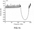
- the figure 1a represents a structure 1 comprising a set of fourteen mechanically connected elements 2 comprising the same piezoelectric material.
- the piezoelectric material comprises titanium lead zirconate or PZT of chemical formula Pb (Zr x Ti 1-x ) O 3 , the elements 2 having a shape of sections.
- a section is a three-dimensional geometrical shape whose height is greater than or equal to the largest dimension of the base.
- the sections are cylindrical in shape of 1 cm in diameter and 1 cm in height.
- the elements 2 are connected to each other via electrodes 3 and polarized perpendicular to the electrodes 3. In this case, the polarizations of two elements 2 of the successive piezoelectric material are opposite and the device is in open circuit, in other words none of the electrodes 3 is connected to the electrical reference 4.
- the figure 1b is a graphical representation of the signal transmitted in decibel of an acoustic wave inside the series of elements 2 as described on the figure 1a depending on the frequency, the frequency range studied being between 0 and 200 kHz.
- the acoustic wave spreads over the entire frequency range studied, no band forbidden frequencies of charge appears.
- the series of piezoelectric material as described on the figure 1a is considered homogeneous from a point of view of the displacement of electric charges.
- the curve of the transmitted signal obtained is identical to the curve of the transmitted signal represented on FIG. figure 1 b.
- the figure 1c represents a set of fourteen elements 2 comprising the same piezoelectric material.
- a section of piezoelectric material comprises lead titano-zirconate or PZT of chemical formula Pb (Zr x Ti 1-x ) O 3 .
- the elements 2 of piezoelectric material are cylindrical in shape of 1 cm in diameter and 1 cm in height.
- the elements 2 are connected to each other via electrodes 3 and polarized perpendicularly to the electrodes.
- the polarization direction d pol is identical to the principal direction d princ elements (2).
- the polarizations of the piezoelectric material of two successive elements 2 are opposite and the device is in a closed circuit. In this case, all the electrodes 3 are directly connected to ground.
- the figure 1d is a graphical representation of the signal transmitted in decibel of an acoustic wave inside the set of elements 2 as described in FIG. figure 1c depending on the frequency, the frequency range studied being between 0 and 200 kHz.
- the transmitted signal drops sharply to a minimum of -130 dB at 150 kHz.
- acoustic waves are greatly attenuated.
- This frequency interval corresponds to a band of forbidden frequencies of charge according to one aspect of the invention.
- a periodic electrical condition is imposed on the series of elements 2 as described on the figure 1a .
- this periodic electrical condition is a grounding of all the electrodes 3 thus generating a displacement of electric charges which generates the appearance of a band of forbidden frequencies of charge according to the principle of the invention.
- the curve of the transmitted signal obtained is identical to the curve of the transmitted signal represented on FIG. figure 1d .
- the type of polarization in the same direction or in opposite directions of the piezoelectric material of the elements 2 has no influence on the presence or absence of forbidden frequency bands of charge. In other words, when the directions of polarization of the elements 2 between two electrical conditions is identical, then the orientation of the polarization has no influence on the characteristics of the forbidden frequency bands of charge generated.
- the figure 1e represents a series of fourteen elements 2 comprising the same piezoelectric material.
- a section of piezoelectric material comprises lead titano-zirconate or PZT of chemical formula Pb (Zr x Ti 1-x ) O 3 .
- the elements 2 of piezoelectric material are cylindrical in shape of 1 cm in diameter and 1 cm in height.
- the elements 2 are connected to each other via electrodes 3 and polarized perpendicularly to the electrodes. Polarization of the material piezoelectric elements 2 successive is in opposite directions and every other electrode is in closed circuit. In this case, every other electrode is connected to ground.
- the figure 1f is a graphical representation of the signal transmitted in decibel of an acoustic wave inside the series of elements 2 as described on the figure 1e depending on the frequency, the frequency range studied being between 0 and 200 kHz.
- the transmitted signal drops sharply to a minimum of -130 dB at 150 kHz.
- acoustic waves are greatly attenuated.
- This frequency interval corresponds to a first load forbidden band already present in the previous case.
- the transmitted signal drops sharply again to a minimum of -95 dB at 75 kHz.
- the acoustic waves are very attenuated. This frequency interval corresponds to a second band of forbidden frequencies of charge.
- the figure 1g represents a set of twenty-eight elements 2 comprising the same piezoelectric material.
- a section of piezoelectric material comprises lead titano-zirconate or PZT of chemical formula Pb (Zr x Ti 1-x ) O 3 .
- the elements 2 of piezoelectric material are cylindrical in shape of 1 cm in diameter and 1 cm in height.
- the elements 2 are connected to each other via electrodes 3 and polarized perpendicularly to the electrodes.
- the polarizations of the piezoelectric material of two successive elements 2 are opposed and the device is in a closed circuit. In this case, all the electrodes 3 are directly connected to ground.
- the figure 1h is a graphical representation of the signal transmitted in decibel of an acoustic wave inside the set of elements 2 as described in FIG. figure 1g depending on the frequency, the frequency range studied being between 0 and 200 kHz.
- the transmitted signal drops sharply to a minimum of below -260 dB at 150 kHz.
- This frequency interval corresponds to a band of forbidden frequencies of charge according to one aspect of the invention.
- the figure 1g and the figure 1h highlight the influence of the number of elements 2.
- the increase in the number of elements 2 increases the attenuation of the transmitted signal in a band of forbidden frequencies of charge.
- a series of fourteen elements 2 comprises the same piezoelectric material comprising lead titano-zirconate or PZT of chemical formula Pb (Zr ⁇ Ti ix ) O 3 in the form of cylindrical sections of 1 cm. of diameter and 1 cm in height, the elements 2 are connected to each other via electrodes 3 and polarized perpendicularly to the electrodes.
- the polarization of the piezoelectric material of two successive elements 2 is in the same direction and one in three electrodes is in a closed circuit. In this case, one in three electrodes is connected to ground. A 50 kHz central frequency load forbidden band appears.
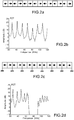
- FIGS. 2a to 2h represent embodiments of the invention as well as the associated transmitted signal curves. These figures illustrate the possibility of frequency shifting the upper and lower terminals of the forbidden charge bands generated by imposing a more complex electrical condition than a simple grounding.
- the figure 2a represents a series of fourteen elements 2 comprising the same piezoelectric material.
- the embodiment of the figure 2a is the same as that of the figure 1a .
- the figure 2b is a graphical representation of the signal transmitted from an acoustic wave inside the series of elements 2 as described in figure 2a as a function of the frequency, the frequency range studied being between 0 and 120 kHz.
- the Figure 2c corresponds to the embodiment of the figure 1e every second electrode is connected to ground.
- the figure 2d represents the curve of the transmitted signal as a function of frequency over a frequency range between 0 and 120 kHz.
- the second band of forbidden frequencies of charge is defined by a center frequency of 80 kHz, a frequency of the upper limit substantially greater than 90 kHz and a frequency of the lower limit substantially lower than 70 kHz.
- the figure 2e represents an embodiment implementing an electrical condition different from a simple grounding 4.
- all the electrodes 3 are connected to ground: an electrode 3 on two is connected directly to the ground 4 and the others are connected to the ground 4 via an impedance 5 in other words the electrodes 3 are alternately connected to the ground 4 and connected to the ground via Impedance 5 may include resistance and / or capacitance and / or inductance. In this case, impedance is a capability.
- the figure 2f represents the curve of the transmitted signal of the series of elements 2 according to the embodiment presented on the figure 2e .
- the frequency of the upper limit of the second forbidden frequency band is of the order of 85 kHz.
- the frequency of the upper bound has been shifted by about 5 kHz towards the low frequencies compared to the embodiment shown in the figure. Figure 2c .
- the figure 2g represents an embodiment in which one electrode 2 out of two is connected to the ground 4 via an impedance 5, the other electrodes 3 are not connected.
- the impedance 5 may be an electrical circuit comprising a resistor and / or a capacitance and / or an inductance. In this case, impedance is a capability.
- the figure 2h represents the curve of the transmitted signal of the series of elements 2 according to the embodiment presented on the figure 2g .
- the frequency of the lower limit of the second band of forbidden frequencies is of the order of 75 kHz.
- the frequency of the lower bound has been shifted by about 5 kHz towards the high frequencies compared to the embodiment shown in Figure 2c .
- a ground connection 4 of all the electrodes 3 by means of two different capacitors alternately enables the upper and lower limits of the forbidden frequency band to be frequency-shifted simultaneously.
- the positive capacities act on the closure of the forbidden band, in other words the lower limit moves towards higher frequencies and the upper limit towards lower frequencies, and vice versa for negative capacities.
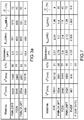
- the choice of the piezoelectric material determines the characteristics of the forbidden bands of charges.
- the figure 3a is a table that presents a list of materials as well as the values of some intrinsic characteristics of materials.
- the intrinsic characteristics may include the constant electric displacement propagation velocity V D and the constant electric field velocity V E of a wave in a material and the electromechanical coupling coefficient k.
- V D The propagation speed with constant electrical displacement
- V E The constant electric field propagation velocity
- the speed of propagation of the wave in the material of the phononic structure determines the thickness of the piezoelectric material, the thickness being called the period spatial and speaking in micrometer.
- the constant electric displacement propagation velocity V D of a wave in a material and the thickness of the elements 2 determine the frequency of the upper limit of the forbidden frequency band.
- the electromechanical coupling coefficient is denoted k. It is a dimensionless size between 0 and 1 that can be expressed as a percentage.
- the coupling coefficient expresses the conversion efficiency of the electrical energy of a piezoelectric material into mechanical energy, and Conversely.
- the coupling coefficient sets the value of the relative frequency width of the load forbidden band.
- the thickness of the elements 2 is set at 10.4 microns. While to open this same band of forbidden frequencies of charge from a series of 10 elements 2 comprising PMN-28PT a thickness of 2.5 microns is sufficient.
- the Figures 3b to 3e represent the calculated curves of the transmitted signal representative of the four piezoelectric materials listed, respectively AIN, a PMN-34.5PT ceramic, a PZ29 ceramic and a PMN-28PT single crystal.
- a series is made comprising ten elements 2, in the form of layers of one of the piezoelectric materials presented on the figure 3a .
- Layer means a geometric structure in which the two dimensions of the base are much greater than the height.
- All ten elements 2 further comprises electrodes 3 disposed between two piezoelectric elements 2. The polarization of all elements 2 is in the same direction. All the electrodes 3 are connected directly to ground 4.
- the figure 3b is a calculated curve of the transmitted signal corresponding to a series of ten elements 2 comprising aluminum nitride or AlN.
- the propagation velocity V D of a wave in the aluminum nitride is 10641 ms -1 , a thickness or spatial period of the elements 2 of 10.4 microns is necessary to generate a band of forbidden frequencies of charge around a frequency of 500 MHz.
- the signal curve transmitted from the AIN has a forbidden frequency band of load between 490 and 510 MHz, the load forbidden band reaches a minimum of -8 dB.
- the figure 3c is a calculated curve of the transmitted signal corresponding to a series of elements 2 comprising the ceramic PMN-34.5PT Pb (Mg 1/2 Nb 2/3 O 3 ) -34.5 PbTiO 3 at a propagation speed V D of 3504 ms -1 .
- the thickness or period necessary to generate a band of forbidden frequencies of charge around 500 MHz is 3.1 microns.
- the curve of the transmitted signal has a forbidden frequency band of load between 449 and 551 MHz, the forbidden band of load reaches a minimum of -40 dB.
- the figure 3d is a calculated curve of the transmitted signal corresponding to a series of elements 2 comprising PZ29.
- PZ29 has a propagation velocity V D of 3840 ms -1 .
- the thickness or spatial period required to generate a forbidden band of charges around 500 MHz is 3.2 microns.
- the curve of the transmitted signal has a band of forbidden frequencies of load between 400 and 600 MHz, the forbidden band of load reaches a minimum of -75 dB.
- the figure 3e is a calculated curve of the transmitted signal corresponding to a series of elements 2 comprising 72Pb (Mg 1/2 Nb 2/3 O 3 ) and 28PbTiO 3 or PMN-28PT monocrystal.
- the single crystal PMN-28PT has a propagation velocity V D of 3424 ms -1 .
- the thickness or the period necessary to generate a band of forbidden frequencies of charges around 500 MHz is 2.5 microns, which is four times smaller than the thickness in the case of AIN.
- the curve of the transmitted signal has a band of forbidden frequencies of load between 321 and 679 MHz, the forbidden band of load reaches a minimum of -120 dB.
- the set of elements 2 comprises a subset of elements 2bis comprising different materials, the subset 2a being repeated periodically.
- the figure 4a represents a structure 1 comprising a sub-assembly 2bis repeated seven times comprising two different piezoelectric materials.
- the first piezoelectric monocrystalline material comprises Pb (Mg 1/2 Nb 2/3 O 3 ) and PbTiO 3 or PMN-28PT and a second material comprises aluminum nitride or AlN.
- the elements 2 having a shape of cylindrically shaped sections of 1 cm in diameter and 1 cm in height.
- the elements 2 are connected to each other via electrodes 3 and polarized perpendicular to the electrodes 3.
- the polarizations of two elements 2 are in the same direction and the device is in open circuit, in other words, none. electrodes 3 is connected to the electrical reference 4.
- the figure 4d is a graphical representation of the signal transmitted in decibel of an acoustic wave inside the series of elements 2 as described on the figure 4a depending on the frequency, the frequency range studied being between 0 and 200 kHz.
- a forbidden frequency band appears, it is centered at about 140 kHz, the forbidden band has a frequency width of about 25 kHz and reaches a minimum of -13 dB.
- the forbidden band corresponds to a band of forbidden frequencies of Bragg.
- the figure 4b represents a structure 1 comprising a set of seven mechanically connected elements 2 comprising the same single-crystal piezoelectric material comprising Pb (Mg 1/2 Nb 2/3 O 3 ) and PbTiO 3 or PMN-28PT.
- the elements 2 having a cylindrical shape of sections 1 cm in diameter and 1 cm in height.
- the elements 2 are connected to each other by means of electrodes 3 and polarized perpendicularly to the electrodes 3. In this case, the polarizations of two elements 2 are in the same direction and the device is in a closed circuit, in other words, all the electrodes 3 are connected directly to the electrical reference 4.
- the figure 4e is a graphical representation of the signal transmitted in decibel of an acoustic wave inside the series of elements 2 as described on the figure 4b depending on the frequency, the frequency range studied being between 0 and 200 kHz.
- a band of forbidden frequencies appears, it is centered at about 140 kHz, the forbidden band has a frequency width of about 100 kHz and reaches a minimum of -83 dB.
- This forbidden band is a band of forbidden frequencies of charge.
- the figure 4c represents a structure 1 comprising a subset 2bis repeated seven times of two different piezoelectric materials.
- a first piezoelectric material comprises Pb (Mg 1/2 Nb 2/3 O 3 ) and PbTiO 3 or PMN-28PT and a second material comprises aluminum nitride AlN.
- the elements 2 having a shape of cylindrical section of 1 cm in diameter and 1 cm in height.
- the elements 2 are connected to each other by means of electrodes 3 and polarized perpendicularly to the electrodes 3.
- the polarizations of two elements 2 are in the same direction and the device is in a closed circuit, in other words, all the electrodes 3 are connected to the electrical reference 4.
- the figure 4f is a graphical representation of the signal transmitted in decibel of an acoustic wave inside the series of elements 2 as described on the figure 4c depending on the frequency, the frequency range studied being between 0 and 200 kHz.
- a band of forbidden frequencies appears, it is centered at about 100 kHz, the forbidden band has a frequency width of about 100 kHz and reaches a minimum of -114 dB.
- elements 2 of Figures 4a and 4c comprise a subset 2bis comprising alternating PMN-28PT and AIN and the elements 2 of the figure 4b include only PMN-28PT.
- This band of forbidden frequencies of the figure 4f corresponding to the embodiment of the figure 4c , cumulates the effects of the forbidden frequency band of Bragg generated by the periodicity resulting from the alternation of materials and a forbidden band of charge generated by the imposition of an electrical condition.
- the cumulative effects can be optimized according to the characteristics of the band of forbidden frequencies that one wishes to obtain. Moreover, it is possible to open or close the forbidden band by modifying the imposed electrical condition.
- a phonon structure 1 with forbidden frequency band provides added value.
- an existing acoustic device such as BAW type resonators and resonators comprising a resonant cavity device
- volume acoustic wave resonators or BAWs make it possible to produce filters with particularly interesting properties in terms of power handling and circuit integration.
- a BAW type resonator an ultra-thin piezoelectric layer deposited between two exciting electrodes of the piezoelectric material is resonated. To maintain a high quality coefficient, this resonator is made on a membrane or decoupled from the substrate by a Bragg mirror.
- the figure 5a represents a BAW resonator according to the prior art.
- the figure 5b represents a BAW resonator according to one aspect of the invention.
- the BAW resonator comprises a layer of piezoelectric material, isolated from the substrate by a phonon structure 1 with a forbidden frequency band, which makes it possible to decouple or couple the resonator with the substrate.
- the integration of a phonon structure 1 with a forbidden frequency band allows a new switch functionality to be added to the BAW resonators.
- the figure 6a presents the geometry of a resonant cavity device based on piezoelectric material, according to the known art.
- the device for electrical excitation is inserted into the cavity, to create a resonator whose frequencies are determined by the width of the cavity.
- the boundaries of the cavity can also be defined by Bragg mirrors. By using a suitable Bragg mirror, only one resonance peak can be preserved.
- the integration of a phonon structure 1 with a band of forbidden frequencies of charge in the structure of the resonator comprising a resonant cavity device makes it possible to define the width of the cavity and therefore its fundamental resonant frequency.
- the figure 6b represents a resonator comprising a resonant cavity device and at least one phonon structure with forbidden bands of charge.
- the grounding or not of the electrodes of the piezoelectric elements located at the ends of the phononic structure makes it possible to mismatch or adapt the impedance of the phononic structure vis-à-vis the cavity and thus move the limits of the cavity.
- the width of the cavity and therefore its resonance frequency can be adjusted over the entire frequency band corresponding to the load forbidden band of the forbidden frequency band phonon structure.
- the Figure 6c represents the modulus of electrical admittance of a resonant cavity as a function of frequency.
- the resonance frequency is 100 kHz in the case of a resonant cavity according to the known art corresponding to the figure 6a .
- the resonant frequency increases when the width of the cavity decreases and vice versa;
- the phonon structure 1 forbidden frequency band of load can be used to create a band of forbidden frequencies around 2 kHz for applications in the field of underwater stealth.
- the forbidden frequency band structure can also be used in the field of aerial stealth by creating forbidden frequency bands around a suitable frequency.
- the figure 7 represents a table comprising a list of piezoelectric materials as well as their intrinsic characteristics and the parameters making it possible to generate a band of forbidden frequencies around 2 kHz.
- the table of the figure 7 shows that with the single crystal PMN-28PT, a thickness of 0.63 m is necessary to generate a band of forbidden frequencies around 2 kHz. Under these conditions, the relative width of the forbidden frequency band is 72%.
- the use of piezoelectric polymers or lead-free materials with lower propagation speeds than other piezoelectric materials would allow for lower layer thicknesses.
- An element 2 of 0.22 m of thickness comprising PVDF makes it possible to generate a band of forbidden frequencies of charge around 2 kHz. However, the relative width of the forbidden frequency band is 0.6%.
- co-polymer comprising poly (vinylidene fluoride) and trifluoroethylene P (VDF-TrFE) with a coupling constant of 65% makes it possible to increase the band gap. It is therefore necessary for submarine stealth applications to achieve a compromise between a coefficient of high coupling allowing a relatively large relative bandwidth and a reasonable material thickness.
- An application of phononic structures 1 band forbidden frequencies of charge consists of the isolation of vibrating structures.
- the figure 8a illustrates this application.
- the idea is to use a phonon structure 1 band forbidden frequencies of charge in order to decouple or isolate a vibrating structure of another structure, capable of emitting radiation, the reference CPIBC designating the band phononic crystal prohibited from charge.
- a damping material may be disposed in the vibrating structure to absorb the reflected energy and to avoid increasing the vibration amplitude.
- FIG. 8b illustrates this application.
- the idea is to use the phonon structure 1 band forbidden frequencies of charge in order to create an irreversible transfer of the vibratory energy from one structure to another.
- a part of the vibratory energy goes from A to B and from B to A.
- the energy can be transferred only in a sense of A to B, for example.
- the Applicant has validated the concept of the present invention by performing a set of experiments described hereinafter, with a 2 cm long ceramic material PZ29 for each element.
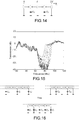
- the figure 9 illustrates the passage of the open-circuit electrodes to short-circuit electrodes for creating a forbidden band, on the interval noted [F inf , F sup ].
- the Figures 10 and 11 illustrate respectively the evolution of the frequency band according to the frequency and the evolution of the wave number standardized.
- the curves C 10a and C 11a relate to the configuration in open circuit mode
- the curves C 10b and C 11b relate to the configuration in short-circuit mode.
- the Applicants have placed a capacitance in place of the short-circuit, as shown in FIG. figure 12 .
- the upper bound of the forbidden band does not vary (F sup ).
- a negative capacitance makes it possible to obtain a forbidden band on the interval [F sup , F] with F> F sup .
- Capacities C1 and C2 can be manipulated to change the width of the bandgap without changing its center frequency ( figure 17 ) or change the center frequency of the bandgap without changing its width ( figure 18 ).
Landscapes
- Physics & Mathematics (AREA)
- Acoustics & Sound (AREA)
- Chemical & Material Sciences (AREA)
- Crystallography & Structural Chemistry (AREA)
- Piezo-Electric Or Mechanical Vibrators, Or Delay Or Filter Circuits (AREA)
Claims (13)
- Akustische Vorrichtung, die eine phononische periodische Struktur (1) mit regelbarer Ladungsbandlücke umfasst, dadurch gekennzeichnet, dass sie Folgendes umfasst:- einen Satz von mechanisch in Serie verbundenen piezoelektrischen Elementen (2), wobei ein piezoelektrisches Element (2) ein piezoelektrisches Material umfasst und in einer Polarisationsrichtung (dpol) polarisiert ist, wobei die Polarisationsrichtungen von zwei aufeinander folgenden Elementen (2) parallel oder antiparallel sind und die piezoelektrischen Elemente (2) gemäß einer Hauptrichtung (dprinc) geleitet werden;- einen Satz von Elektroden (3), die zwischen zwei benachbarten piezoelektrischen Elementen (2) und lotrecht zur Hauptrichtung angeordnet sind;- wobei der Elektrodensatz wenigstens einen Teilsatz von Elektroden umfasst, die auf periodische Weise mit einer externen elektrischen Referenz (4) verbunden sind;- wobei der Elektrodenteilsatz mit der elektrischen Referenz (4) über einen elektrischen Stromkreis (5) verbunden ist,wobei die regelbare Bandlücke erscheint, wenn eine Bewegung von elektrischen Ladungen von einer externen elektrischen Referenz über eine Elektrode des Elektrodensatzes stammt.
- Akustische Vorrichtung nach Anspruch 1, ausgelegt zum Steuern des elektrischen Stromkreises auf der Basis von von einem externen Sensor empfangenen Daten.
- Vorrichtung nach einem der vorherigen Ansprüche, bei der die piezoelektrischen Elemente (2) ein selbes piezoelektrisches Material umfassen.
- Akustische Vorrichtung nach einem der vorherigen Ansprüche, die ferner wenigstens ein dielektrisches Element (2) umfasst.
- Akustische Vorrichtung nach einem der vorherigen Ansprüche, wobei die elektrische Referenz (4) Masse ist.
- Akustische Vorrichtung nach einem der vorherigen Ansprüche, wobei die elektrische Referenz eine externe Spannungsquelle (4) ist.
- Akustische Vorrichtung nach einem der vorherigen Ansprüche, bei der die Elemente (2) die Form von Platten oder die Form von Abschnitten haben.
- Akustische Vorrichtung nach einem der vorherigen Ansprüche, bei der die Polarisationsrichtung mit der Hauptrichtung identisch ist.
- BAW-Resonator, der eine akustische Vorrichtung nach den Ansprüchen 1 bis 8 umfasst.
- Vorrichtung mit Resonanzhohlraum, die eine akustische Vorrichtung nach den Ansprüchen 1 bis 8 umfasst.
- Vorrichtung zum Isolieren einer vibrierenden Struktur, die eine akustische Vorrichtung nach den Ansprüchen 1 bis 8 umfasst.
- Isolationsvorrichtung nach Anspruch 11, die ferner eine Dämpfungsstruktur umfasst.
- Vorrichtung zum Übertragen von Energie von einer ersten vibrierenden Struktur zu einer zweiten vibrierenden Struktur, die eine akustische Vorrichtung nach den Ansprüchen 1 bis 8 umfasst.
Applications Claiming Priority (2)
| Application Number | Priority Date | Filing Date | Title |
|---|---|---|---|
| FR1202561A FR2996080B1 (fr) | 2012-09-27 | 2012-09-27 | Dispositif acoustique comprenant un cristal phononique reglable |
| PCT/EP2013/070052 WO2014049045A1 (fr) | 2012-09-27 | 2013-09-26 | Dispositif acoustique comprenant un cristal phononique reglable a base d'elements piezoelectriques |
Publications (2)
| Publication Number | Publication Date |
|---|---|
| EP2901551A1 EP2901551A1 (de) | 2015-08-05 |
| EP2901551B1 true EP2901551B1 (de) | 2018-04-18 |
Family
ID=47989029
Family Applications (1)
| Application Number | Title | Priority Date | Filing Date |
|---|---|---|---|
| EP13766547.7A Active EP2901551B1 (de) | 2012-09-27 | 2013-09-26 | Elektroakustische vorrichtung enthaltend einen regelbaren phononischen kristall mit piezoelektrischen elementen |
Country Status (3)
| Country | Link |
|---|---|
| EP (1) | EP2901551B1 (de) |
| FR (1) | FR2996080B1 (de) |
| WO (1) | WO2014049045A1 (de) |
Families Citing this family (2)
| Publication number | Priority date | Publication date | Assignee | Title |
|---|---|---|---|---|
| CN107045868B (zh) * | 2017-01-09 | 2020-03-06 | 温州大学 | 一种局域共振型声子晶体周期涂层结构 |
| CN106981286B (zh) * | 2017-04-21 | 2021-01-26 | 广东工业大学 | 声波传导介质及声斜入射全反射的实现方法 |
Family Cites Families (4)
| Publication number | Priority date | Publication date | Assignee | Title |
|---|---|---|---|---|
| JPH118526A (ja) * | 1997-04-25 | 1999-01-12 | Murata Mfg Co Ltd | 圧電共振子およびそれを用いた電子部品 |
| TW432731B (en) * | 1998-12-01 | 2001-05-01 | Murata Manufacturing Co | Multilayer piezoelectric part |
| DE10149542A1 (de) * | 2001-10-08 | 2003-04-17 | Infineon Technologies Ag | BAW-Resonator |
| US7969073B2 (en) * | 2007-12-18 | 2011-06-28 | Trs Technologies, Inc. | Tangentially poled single crystal ring resonator |
-
2012
- 2012-09-27 FR FR1202561A patent/FR2996080B1/fr not_active Expired - Fee Related
-
2013
- 2013-09-26 EP EP13766547.7A patent/EP2901551B1/de active Active
- 2013-09-26 WO PCT/EP2013/070052 patent/WO2014049045A1/fr active Application Filing
Non-Patent Citations (1)
| Title |
|---|
| None * |
Also Published As
| Publication number | Publication date |
|---|---|
| FR2996080B1 (fr) | 2016-01-15 |
| WO2014049045A1 (fr) | 2014-04-03 |
| FR2996080A1 (fr) | 2014-03-28 |
| EP2901551A1 (de) | 2015-08-05 |
Similar Documents
| Publication | Publication Date | Title |
|---|---|---|
| EP3010149B1 (de) | Resonanzschaltung mit variabler frequenz und impedanz | |
| EP2628242B1 (de) | Oberflächenschallwellen-bandpassfilter mit integrierter akustischer führung mit impedanz- und/oder modusumwandlung | |
| FR2905208A1 (fr) | Filtre a resonateurs a ondes de lamb couples. | |
| EP2203976B1 (de) | Lambwellenresonator | |
| EP2278708B1 (de) | Mit geführten akustischen Wellen arbeitende Resonanzvorrichtung und Herstellungsverfahren | |
| EP2628245B1 (de) | Lateral gekoppeltes baw-filter mit phononischen kristallen | |
| FR2905207A1 (fr) | Filtre commutable a resonateurs. | |
| FR2974691B1 (fr) | Dispositif electromecanique a ondes acoustiques comprenant une zone de transduction et une cavite etendue | |
| FR2484735A1 (fr) | Resonateur a ondes acoustiques de surface | |
| FR2834593A1 (fr) | Resonateur piezoelectrique et filtre piezoelectrique, duplexeur et appareil de communication l'incluant | |
| EP1053593B1 (de) | Resonatorfilter mit akustischen oberflächenwellen | |
| FR3115428A1 (fr) | Dispositif électromécanique à fréquence de résonance ajustable | |
| EP2341617A1 (de) | Akustischer Resonator, der ein Elektret umfasst, sowie Herstellungsverfahren dieses Resonators und Anwendung auf gekoppelte Resonatoren bei umschaltbaren Filtern | |
| EP2901551B1 (de) | Elektroakustische vorrichtung enthaltend einen regelbaren phononischen kristall mit piezoelektrischen elementen | |
| EP2385625B1 (de) | Kombinierer mit akustischem Wandler | |
| WO1994007307A1 (fr) | Transducteur d'ondes unidirectionnel | |
| FR2904492A1 (fr) | Circuit de filtrage dote de resonateurs acoustiques | |
| EP3032742A2 (de) | Elastische oberflächenwellen verwendende sensorvorrichtung geeignet zur fernabfrage | |
| EP2587668B1 (de) | Leistungskoppler verwendend akustische Wellen | |
| FR2653632A1 (fr) | Transducteur d'ondes de surface unidirectionnel. | |
| EP3903417B1 (de) | Verbesserte oberflächenschallwellenvorrichtung | |
| FR3079101A1 (fr) | Structure de transducteur pour suppression de source dans les dispositifs de filtres a ondes acoustiques de surface | |
| WO2003088482A1 (fr) | Module comprenant des composants a ondes acoustiques d'interface | |
| CH624802A5 (de) | ||
| CH710638A2 (fr) | Un filtre-transformateur piézoélectrique à ondes élastiques de volume. |
Legal Events
| Date | Code | Title | Description |
|---|---|---|---|
| PUAI | Public reference made under article 153(3) epc to a published international application that has entered the european phase |
Free format text: ORIGINAL CODE: 0009012 |
|
| 17P | Request for examination filed |
Effective date: 20150409 |
|
| AK | Designated contracting states |
Kind code of ref document: A1 Designated state(s): AL AT BE BG CH CY CZ DE DK EE ES FI FR GB GR HR HU IE IS IT LI LT LU LV MC MK MT NL NO PL PT RO RS SE SI SK SM TR |
|
| AX | Request for extension of the european patent |
Extension state: BA ME |
|
| DAX | Request for extension of the european patent (deleted) | ||
| RAP1 | Party data changed (applicant data changed or rights of an application transferred) |
Owner name: THALES |
|
| 17Q | First examination report despatched |
Effective date: 20170109 |
|
| GRAP | Despatch of communication of intention to grant a patent |
Free format text: ORIGINAL CODE: EPIDOSNIGR1 |
|
| INTG | Intention to grant announced |
Effective date: 20171109 |
|
| GRAS | Grant fee paid |
Free format text: ORIGINAL CODE: EPIDOSNIGR3 |
|
| GRAA | (expected) grant |
Free format text: ORIGINAL CODE: 0009210 |
|
| AK | Designated contracting states |
Kind code of ref document: B1 Designated state(s): AL AT BE BG CH CY CZ DE DK EE ES FI FR GB GR HR HU IE IS IT LI LT LU LV MC MK MT NL NO PL PT RO RS SE SI SK SM TR |
|
| REG | Reference to a national code |
Ref country code: GB Ref legal event code: FG4D Free format text: NOT ENGLISH |
|
| REG | Reference to a national code |
Ref country code: CH Ref legal event code: EP |
|
| REG | Reference to a national code |
Ref country code: DE Ref legal event code: R096 Ref document number: 602013036126 Country of ref document: DE |
|
| REG | Reference to a national code |
Ref country code: AT Ref legal event code: REF Ref document number: 991489 Country of ref document: AT Kind code of ref document: T Effective date: 20180515 |
|
| REG | Reference to a national code |
Ref country code: IE Ref legal event code: FG4D Free format text: LANGUAGE OF EP DOCUMENT: FRENCH |
|
| REG | Reference to a national code |
Ref country code: NL Ref legal event code: MP Effective date: 20180418 |
|
| REG | Reference to a national code |
Ref country code: FR Ref legal event code: PLFP Year of fee payment: 6 |
|
| REG | Reference to a national code |
Ref country code: LT Ref legal event code: MG4D |
|
| PG25 | Lapsed in a contracting state [announced via postgrant information from national office to epo] |
Ref country code: NL Free format text: LAPSE BECAUSE OF FAILURE TO SUBMIT A TRANSLATION OF THE DESCRIPTION OR TO PAY THE FEE WITHIN THE PRESCRIBED TIME-LIMIT Effective date: 20180418 |
|
| PG25 | Lapsed in a contracting state [announced via postgrant information from national office to epo] |
Ref country code: AL Free format text: LAPSE BECAUSE OF FAILURE TO SUBMIT A TRANSLATION OF THE DESCRIPTION OR TO PAY THE FEE WITHIN THE PRESCRIBED TIME-LIMIT Effective date: 20180418 Ref country code: BG Free format text: LAPSE BECAUSE OF FAILURE TO SUBMIT A TRANSLATION OF THE DESCRIPTION OR TO PAY THE FEE WITHIN THE PRESCRIBED TIME-LIMIT Effective date: 20180718 Ref country code: FI Free format text: LAPSE BECAUSE OF FAILURE TO SUBMIT A TRANSLATION OF THE DESCRIPTION OR TO PAY THE FEE WITHIN THE PRESCRIBED TIME-LIMIT Effective date: 20180418 Ref country code: LT Free format text: LAPSE BECAUSE OF FAILURE TO SUBMIT A TRANSLATION OF THE DESCRIPTION OR TO PAY THE FEE WITHIN THE PRESCRIBED TIME-LIMIT Effective date: 20180418 Ref country code: PL Free format text: LAPSE BECAUSE OF FAILURE TO SUBMIT A TRANSLATION OF THE DESCRIPTION OR TO PAY THE FEE WITHIN THE PRESCRIBED TIME-LIMIT Effective date: 20180418 Ref country code: SE Free format text: LAPSE BECAUSE OF FAILURE TO SUBMIT A TRANSLATION OF THE DESCRIPTION OR TO PAY THE FEE WITHIN THE PRESCRIBED TIME-LIMIT Effective date: 20180418 Ref country code: NO Free format text: LAPSE BECAUSE OF FAILURE TO SUBMIT A TRANSLATION OF THE DESCRIPTION OR TO PAY THE FEE WITHIN THE PRESCRIBED TIME-LIMIT Effective date: 20180718 Ref country code: ES Free format text: LAPSE BECAUSE OF FAILURE TO SUBMIT A TRANSLATION OF THE DESCRIPTION OR TO PAY THE FEE WITHIN THE PRESCRIBED TIME-LIMIT Effective date: 20180418 |
|
| PG25 | Lapsed in a contracting state [announced via postgrant information from national office to epo] |
Ref country code: GR Free format text: LAPSE BECAUSE OF FAILURE TO SUBMIT A TRANSLATION OF THE DESCRIPTION OR TO PAY THE FEE WITHIN THE PRESCRIBED TIME-LIMIT Effective date: 20180719 Ref country code: HR Free format text: LAPSE BECAUSE OF FAILURE TO SUBMIT A TRANSLATION OF THE DESCRIPTION OR TO PAY THE FEE WITHIN THE PRESCRIBED TIME-LIMIT Effective date: 20180418 Ref country code: LV Free format text: LAPSE BECAUSE OF FAILURE TO SUBMIT A TRANSLATION OF THE DESCRIPTION OR TO PAY THE FEE WITHIN THE PRESCRIBED TIME-LIMIT Effective date: 20180418 Ref country code: RS Free format text: LAPSE BECAUSE OF FAILURE TO SUBMIT A TRANSLATION OF THE DESCRIPTION OR TO PAY THE FEE WITHIN THE PRESCRIBED TIME-LIMIT Effective date: 20180418 |
|
| REG | Reference to a national code |
Ref country code: AT Ref legal event code: MK05 Ref document number: 991489 Country of ref document: AT Kind code of ref document: T Effective date: 20180418 |
|
| PG25 | Lapsed in a contracting state [announced via postgrant information from national office to epo] |
Ref country code: PT Free format text: LAPSE BECAUSE OF FAILURE TO SUBMIT A TRANSLATION OF THE DESCRIPTION OR TO PAY THE FEE WITHIN THE PRESCRIBED TIME-LIMIT Effective date: 20180820 |
|
| REG | Reference to a national code |
Ref country code: DE Ref legal event code: R097 Ref document number: 602013036126 Country of ref document: DE |
|
| PG25 | Lapsed in a contracting state [announced via postgrant information from national office to epo] |
Ref country code: SK Free format text: LAPSE BECAUSE OF FAILURE TO SUBMIT A TRANSLATION OF THE DESCRIPTION OR TO PAY THE FEE WITHIN THE PRESCRIBED TIME-LIMIT Effective date: 20180418 Ref country code: EE Free format text: LAPSE BECAUSE OF FAILURE TO SUBMIT A TRANSLATION OF THE DESCRIPTION OR TO PAY THE FEE WITHIN THE PRESCRIBED TIME-LIMIT Effective date: 20180418 Ref country code: CZ Free format text: LAPSE BECAUSE OF FAILURE TO SUBMIT A TRANSLATION OF THE DESCRIPTION OR TO PAY THE FEE WITHIN THE PRESCRIBED TIME-LIMIT Effective date: 20180418 Ref country code: RO Free format text: LAPSE BECAUSE OF FAILURE TO SUBMIT A TRANSLATION OF THE DESCRIPTION OR TO PAY THE FEE WITHIN THE PRESCRIBED TIME-LIMIT Effective date: 20180418 Ref country code: DK Free format text: LAPSE BECAUSE OF FAILURE TO SUBMIT A TRANSLATION OF THE DESCRIPTION OR TO PAY THE FEE WITHIN THE PRESCRIBED TIME-LIMIT Effective date: 20180418 Ref country code: AT Free format text: LAPSE BECAUSE OF FAILURE TO SUBMIT A TRANSLATION OF THE DESCRIPTION OR TO PAY THE FEE WITHIN THE PRESCRIBED TIME-LIMIT Effective date: 20180418 |
|
| PLBE | No opposition filed within time limit |
Free format text: ORIGINAL CODE: 0009261 |
|
| STAA | Information on the status of an ep patent application or granted ep patent |
Free format text: STATUS: NO OPPOSITION FILED WITHIN TIME LIMIT |
|
| PG25 | Lapsed in a contracting state [announced via postgrant information from national office to epo] |
Ref country code: IT Free format text: LAPSE BECAUSE OF FAILURE TO SUBMIT A TRANSLATION OF THE DESCRIPTION OR TO PAY THE FEE WITHIN THE PRESCRIBED TIME-LIMIT Effective date: 20180418 Ref country code: SM Free format text: LAPSE BECAUSE OF FAILURE TO SUBMIT A TRANSLATION OF THE DESCRIPTION OR TO PAY THE FEE WITHIN THE PRESCRIBED TIME-LIMIT Effective date: 20180418 |
|
| 26N | No opposition filed |
Effective date: 20190121 |
|
| REG | Reference to a national code |
Ref country code: DE Ref legal event code: R119 Ref document number: 602013036126 Country of ref document: DE |
|
| PG25 | Lapsed in a contracting state [announced via postgrant information from national office to epo] |
Ref country code: MC Free format text: LAPSE BECAUSE OF FAILURE TO SUBMIT A TRANSLATION OF THE DESCRIPTION OR TO PAY THE FEE WITHIN THE PRESCRIBED TIME-LIMIT Effective date: 20180418 |
|
| REG | Reference to a national code |
Ref country code: CH Ref legal event code: PL |
|
| GBPC | Gb: european patent ceased through non-payment of renewal fee |
Effective date: 20180926 |
|
| PG25 | Lapsed in a contracting state [announced via postgrant information from national office to epo] |
Ref country code: SI Free format text: LAPSE BECAUSE OF FAILURE TO SUBMIT A TRANSLATION OF THE DESCRIPTION OR TO PAY THE FEE WITHIN THE PRESCRIBED TIME-LIMIT Effective date: 20180418 |
|
| REG | Reference to a national code |
Ref country code: BE Ref legal event code: MM Effective date: 20180930 |
|
| REG | Reference to a national code |
Ref country code: IE Ref legal event code: MM4A |
|
| PG25 | Lapsed in a contracting state [announced via postgrant information from national office to epo] |
Ref country code: LU Free format text: LAPSE BECAUSE OF NON-PAYMENT OF DUE FEES Effective date: 20180926 |
|
| PG25 | Lapsed in a contracting state [announced via postgrant information from national office to epo] |
Ref country code: IE Free format text: LAPSE BECAUSE OF NON-PAYMENT OF DUE FEES Effective date: 20180926 Ref country code: DE Free format text: LAPSE BECAUSE OF NON-PAYMENT OF DUE FEES Effective date: 20190402 |
|
| PG25 | Lapsed in a contracting state [announced via postgrant information from national office to epo] |
Ref country code: CH Free format text: LAPSE BECAUSE OF NON-PAYMENT OF DUE FEES Effective date: 20180930 Ref country code: LI Free format text: LAPSE BECAUSE OF NON-PAYMENT OF DUE FEES Effective date: 20180930 Ref country code: BE Free format text: LAPSE BECAUSE OF NON-PAYMENT OF DUE FEES Effective date: 20180930 |
|
| PG25 | Lapsed in a contracting state [announced via postgrant information from national office to epo] |
Ref country code: GB Free format text: LAPSE BECAUSE OF NON-PAYMENT OF DUE FEES Effective date: 20180926 |
|
| PG25 | Lapsed in a contracting state [announced via postgrant information from national office to epo] |
Ref country code: MT Free format text: LAPSE BECAUSE OF FAILURE TO SUBMIT A TRANSLATION OF THE DESCRIPTION OR TO PAY THE FEE WITHIN THE PRESCRIBED TIME-LIMIT Effective date: 20180418 |
|
| PG25 | Lapsed in a contracting state [announced via postgrant information from national office to epo] |
Ref country code: TR Free format text: LAPSE BECAUSE OF FAILURE TO SUBMIT A TRANSLATION OF THE DESCRIPTION OR TO PAY THE FEE WITHIN THE PRESCRIBED TIME-LIMIT Effective date: 20180418 |
|
| PG25 | Lapsed in a contracting state [announced via postgrant information from national office to epo] |
Ref country code: HU Free format text: LAPSE BECAUSE OF FAILURE TO SUBMIT A TRANSLATION OF THE DESCRIPTION OR TO PAY THE FEE WITHIN THE PRESCRIBED TIME-LIMIT; INVALID AB INITIO Effective date: 20130926 Ref country code: MK Free format text: LAPSE BECAUSE OF NON-PAYMENT OF DUE FEES Effective date: 20180418 Ref country code: CY Free format text: LAPSE BECAUSE OF FAILURE TO SUBMIT A TRANSLATION OF THE DESCRIPTION OR TO PAY THE FEE WITHIN THE PRESCRIBED TIME-LIMIT Effective date: 20180418 |
|
| PG25 | Lapsed in a contracting state [announced via postgrant information from national office to epo] |
Ref country code: IS Free format text: LAPSE BECAUSE OF FAILURE TO SUBMIT A TRANSLATION OF THE DESCRIPTION OR TO PAY THE FEE WITHIN THE PRESCRIBED TIME-LIMIT Effective date: 20180818 |
|
| PGFP | Annual fee paid to national office [announced via postgrant information from national office to epo] |
Ref country code: FR Payment date: 20240821 Year of fee payment: 12 |