EP2901504B1 - Electrical component and method for establishing contact with an electrical component - Google Patents
Electrical component and method for establishing contact with an electrical component Download PDFInfo
- Publication number
- EP2901504B1 EP2901504B1 EP13762093.6A EP13762093A EP2901504B1 EP 2901504 B1 EP2901504 B1 EP 2901504B1 EP 13762093 A EP13762093 A EP 13762093A EP 2901504 B1 EP2901504 B1 EP 2901504B1
- Authority
- EP
- European Patent Office
- Prior art keywords
- metallization
- electrical component
- contact
- contact element
- component according
- Prior art date
- Legal status (The legal status is an assumption and is not a legal conclusion. Google has not performed a legal analysis and makes no representation as to the accuracy of the status listed.)
- Active
Links
- 238000000034 method Methods 0.000 title claims description 12
- 238000001465 metallisation Methods 0.000 claims description 222
- 239000000463 material Substances 0.000 claims description 25
- 229910000679 solder Inorganic materials 0.000 claims description 24
- 239000011521 glass Substances 0.000 claims description 22
- 239000002346 layers by function Substances 0.000 claims description 8
- 239000004744 fabric Substances 0.000 claims description 3
- 238000010304 firing Methods 0.000 claims description 3
- 239000010410 layer Substances 0.000 description 22
- RYGMFSIKBFXOCR-UHFFFAOYSA-N Copper Chemical compound [Cu] RYGMFSIKBFXOCR-UHFFFAOYSA-N 0.000 description 8
- 229910052802 copper Inorganic materials 0.000 description 8
- 239000010949 copper Substances 0.000 description 8
- BQCADISMDOOEFD-UHFFFAOYSA-N Silver Chemical compound [Ag] BQCADISMDOOEFD-UHFFFAOYSA-N 0.000 description 6
- 229910052709 silver Inorganic materials 0.000 description 6
- 239000004332 silver Substances 0.000 description 6
- 238000004519 manufacturing process Methods 0.000 description 5
- 229910052751 metal Inorganic materials 0.000 description 5
- 239000002184 metal Substances 0.000 description 5
- 238000007650 screen-printing Methods 0.000 description 4
- 238000005476 soldering Methods 0.000 description 4
- 238000010586 diagram Methods 0.000 description 3
- 238000003466 welding Methods 0.000 description 3
- 229910010293 ceramic material Inorganic materials 0.000 description 2
- 238000009792 diffusion process Methods 0.000 description 2
- 238000009826 distribution Methods 0.000 description 2
- SWELZOZIOHGSPA-UHFFFAOYSA-N palladium silver Chemical compound [Pd].[Ag] SWELZOZIOHGSPA-UHFFFAOYSA-N 0.000 description 2
- QCEUXSAXTBNJGO-UHFFFAOYSA-N [Ag].[Sn] Chemical compound [Ag].[Sn] QCEUXSAXTBNJGO-UHFFFAOYSA-N 0.000 description 1
- 239000000853 adhesive Substances 0.000 description 1
- 230000001070 adhesive effect Effects 0.000 description 1
- 239000000919 ceramic Substances 0.000 description 1
- 239000011888 foil Substances 0.000 description 1
- 238000010438 heat treatment Methods 0.000 description 1
- 230000001771 impaired effect Effects 0.000 description 1
- 238000002347 injection Methods 0.000 description 1
- 239000007924 injection Substances 0.000 description 1
- 239000002655 kraft paper Substances 0.000 description 1
- 150000002739 metals Chemical class 0.000 description 1
- 239000012299 nitrogen atmosphere Substances 0.000 description 1
- 230000010287 polarization Effects 0.000 description 1
- 229920003223 poly(pyromellitimide-1,4-diphenyl ether) Polymers 0.000 description 1
Images

Classifications
-
- H—ELECTRICITY
- H01—ELECTRIC ELEMENTS
- H01H—ELECTRIC SWITCHES; RELAYS; SELECTORS; EMERGENCY PROTECTIVE DEVICES
- H01H57/00—Electrostrictive relays; Piezo-electric relays
-
- H—ELECTRICITY
- H01—ELECTRIC ELEMENTS
- H01H—ELECTRIC SWITCHES; RELAYS; SELECTORS; EMERGENCY PROTECTIVE DEVICES
- H01H45/00—Details of relays
- H01H45/14—Terminal arrangements
-
- H—ELECTRICITY
- H01—ELECTRIC ELEMENTS
- H01H—ELECTRIC SWITCHES; RELAYS; SELECTORS; EMERGENCY PROTECTIVE DEVICES
- H01H49/00—Apparatus or processes specially adapted to the manufacture of relays or parts thereof
-
- H—ELECTRICITY
- H10—SEMICONDUCTOR DEVICES; ELECTRIC SOLID-STATE DEVICES NOT OTHERWISE PROVIDED FOR
- H10N—ELECTRIC SOLID-STATE DEVICES NOT OTHERWISE PROVIDED FOR
- H10N30/00—Piezoelectric or electrostrictive devices
- H10N30/01—Manufacture or treatment
- H10N30/06—Forming electrodes or interconnections, e.g. leads or terminals
- H10N30/063—Forming interconnections, e.g. connection electrodes of multilayered piezoelectric or electrostrictive parts
-
- H—ELECTRICITY
- H10—SEMICONDUCTOR DEVICES; ELECTRIC SOLID-STATE DEVICES NOT OTHERWISE PROVIDED FOR
- H10N—ELECTRIC SOLID-STATE DEVICES NOT OTHERWISE PROVIDED FOR
- H10N30/00—Piezoelectric or electrostrictive devices
- H10N30/80—Constructional details
- H10N30/87—Electrodes or interconnections, e.g. leads or terminals
- H10N30/872—Connection electrodes of multilayer piezoelectric or electrostrictive devices, e.g. external electrodes
Definitions
- An electrical component comprising at least one metallization is specified.
- the metallization is provided for contacting internal electrodes of the component.
- the electrical component is formed for example as a piezoelectric actuator.
- a method for producing a contact of an electrical component is specified.
- a piezoactuator which has an external contact, in which a wire mesh is attached to a base metallization.
- EP 0844678 B1 is a piezoelectric actuator specified, which has a three-dimensionally structured, electrically conductive electrode which is connected via partial contact points with a base metallization.
- EP 2 437 322 A1 For example, a piezoelectric device with a two-layered baked external electrode is known, the upper layer only partially covering the lower one.
- a similar device disclosed US 2008/007144 A1 wherein the upper layer comprises either two strips or a rectangular frame and is mounted on this approximately a conductive grid. It is an object to be solved to provide an improved electrical component. Furthermore, it is an object to be solved to provide a method for producing an electrical component.
- the component is designed as a piezoelectric actuator, in particular as a piezoelectric actuator for actuating an injection valve in a motor vehicle.
- the component preferably has a body on.
- the main body preferably has internal electrodes.
- the internal electrodes are formed, for example, as electrode layers.
- the component is designed as a multilayer component, wherein functional layers and electrode layers are alternately stacked on top of each other.
- the functional layers are, for example, piezoelectric layers, in particular piezoceramic layers.
- the inner electrodes preferably extend in the stacking direction alternately to an outer side of the main body and are spaced from the opposite outer side.
- the stack of electrode layers and functional layers is preferably formed as a monolithic sintered body.
- the electrical component has at least one external contact having at least one metallization.
- the external contact is preferably designed for contacting internal electrodes of the main body.
- the metallization is preferably arranged on an outer side of the base body. Preferably, the metallization is layered. The metallization preferably contacts every second inner electrode. For contacting the further inner electrodes, a further metallization may be provided which is arranged, for example, on an opposite outer side of the base body.
- the electrical component has an external contact with a first metallization and a second metallization, wherein the second metallization is arranged on the first metallization.
- the first metallization is preferably arranged directly on an outer side of the base body and preferably in direct electrical contact with inner electrodes of the base body.
- the metallizations are preferably used for electrical contacting of the internal electrodes. Both metallizations are formed as burned metallizations.
- the first metallization only partially covers the second metallization.
- a metallic paste is applied to an outer side of the base body. Subsequently, the metallic paste, for example, baked at a temperature in the range of 500 ° C to 900 ° C.
- a first metallic paste is applied to an outside of the base body and baked to produce the first metallization. Subsequently, a second metallic paste is applied to the first metallization and baked to produce the second metallization.
- mixing of the materials of the metallizations can be particularly well prevented. In particular, diffusion of material components from one of the metallizations into the other metallization can be prevented.
- the first and the second metallization have a different wettability with solder material.
- the solder material is a tin-silver solder.
- a contact element which is to be attached to at least one of the metallizations is sufficiently strong attached to one of the two metallizations and is less well or not attached to the other metallization.
- a mounting area of the contact element can be determined by the shape of the metallization having the higher wettability.
- the first metallization has a lower wettability with solder material than the second metallization.
- the contact element can be provided over a large area with solder material and placed on the metallizations.
- solder material can be applied over a large area to the exposed surfaces of the metallizations. Subsequently, a soldering process is performed. Due to the different wettability of the metallization with solder material, the contact element adheres well to the second metallization and less well or not to the first metallization.
- the first metallization has a glass component and the second metallization has no glass component or a smaller glass component than the first metalization.
- the glass content in the first metallization Due to the glass content in the first metallization, a particularly firm connection of the first metallization with the base body, in particular with ceramic layers of the base body, can be achieved. Due to the missing or lower glass content of the second metallization, the wettability of the second metallization with solder material is preferably increased in comparison to the first metallization. According to the invention, the second metallization has a smaller area than the first metallization.
- the main surface of a layered metallization is preferably designated by the surface of the respective metallization.
- the main surface preferably runs parallel to the outside of the main body on which the metallizations are arranged.
- a good connection to the main body can be achieved. Due to the smaller area of the second metallization, a contact element can be fastened in a desired, smaller area, so that, for example, the flexibility of the contact element through the attachment area is only slightly impaired. As a result, in particular cracks in the main body can be bridged by the contact element.
- the first metallization is for example formed over the entire surface. This means that the first metallization is formed as a continuous surface and has no recesses.
- the second metallization has at least one recess.
- the second metallization is U-shaped.
- two partial sections arranged in parallel are connected to one another at one end of the partial areas by a third partial area.
- a contact element is attached to at least one of the metallizations.
- the contact element is attached to the second metallization.
- the contact element is flexible. In this way, the contact element yield under mechanical stress without tearing. In particular, the contact element can bridge cracks that occur in the body, and thus ensure a reliable electrical connection of the device.
- the contact element has at least one recess.
- the contact element may have a mesh or fabric structure.
- the contact element has, for example, a plurality of wires.
- the contact element may be formed as a wire mesh or wire mesh be.
- the contact element may also be formed as a metallic sheet. In the metallic sheet one or more recesses may be provided, for example circular recesses.
- the contact element is preferably soldered to at least one of the metallizations.
- the contact element is soldered to the second metallization.
- the contact element may additionally be soldered to the first metallization.
- the contact element is not soldered or only with low adhesion to the first metallization.
- At least one lateral edge region of the contact element is attached directly to the second metallization.
- no part of the edge region protrudes beyond the second metallization.
- the contact element is fastened to the frame and does not protrude laterally beyond the frame.
- the contact element can be fastened to the second metallization at three lateral edge regions. The contact element preferably does not project laterally beyond the first metallization.
- a further contact is attached to the contact element.
- the further contact is preferably used for the electrical connection of the device a voltage source.
- the further contact has a wire or a plurality of wires.
- the further contact is designed as a contact pin.
- the further contacting is preferably not arranged above the second metallization.
- the term "above” designates the direction of the surface normal of the outside of the base body provided with the second metallization.
- the further contacting is not arranged above a fastening region of the contact element on one of the metallizations. In this way, the further contact can be attached particularly well to the contact element, without damaging the device occurs.
- the further contact is welded to the contact element.
- the further contact can be pressed against the contact element during the fastening step. If the contact element in this area is not fastened directly to a metallization, the contact element can yield, for example, whereby a good contact of the contact element with the further contact can be achieved. Furthermore, in this case, in the fastening step, in particular a welding or soldering, the base metallization is not damaged.
- the further contacting is preferably arranged at least partially above the first metallization.
- the further contacting extends through the opening of the U-shaped region into the interior of the U-shaped region.
- an electrical component with at least one external contact having at least one metallization is specified, wherein the metallization is designed as a frame, wherein the frame shape of the metallization has an opening, so that the frame shape is U-shaped.
- a contact element is attached to the frame-shaped metallization as described above.
- at least one lateral edge region of the contact element is fastened directly to the frame.
- a further contact in particular be attached in the form of a contact pin on the contact element.
- a method for producing an electrical contacting of an electrical component is specified.
- a main body of an electrical component is provided and a first metallic paste is applied to an outer side of the main body.
- the first metallic paste is baked to form a first metallization.
- a second metallic paste is applied to the first metallization and then the second metallic paste is baked.
- the method produces the components described above, wherein the components used in the method have all the functional and structural properties of the components of the components described above.
- At least one of the metallizations a contact element attached, in particular soldered.
- the contact element for example, generously coated with solder material.
- the first and second metallizations may have different wettability with solder material. In this way it can be achieved that the contact element is attached only to one of the metallizations and not or only slightly on the other metallization is attached. Furthermore, a further contact can be attached to the contact element as described above, for example, welded.
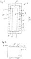
- FIG. 1 shows a plan view of an electrical component. 1
- FIG. 2 shows a cross section of the device FIG. 1 ,
- the electrical component 1 is preferably a piezoelectric component, in particular a piezoelectric actuator.
- the component 1 is designed as a multilayer component.
- the component 1 has a main body 2, in which first and second internal electrodes 3, 4 and functional layers 5 are alternately stacked along a stacking direction S.
- the inner electrodes 3, 4 extend alternately to an outer side 6 of the main body 2 and are spaced from an opposite outer side (not shown).
- the internal electrodes 3, 4 contain copper, silver, or silver-palladium.
- the functional layers 5 are formed, for example, as dielectric layers, in particular as piezoelectric layers.
- the functional layers 5 may be formed of a ceramic material, in particular be formed as piezoceramic layers.
- the device 1 expands upon application of a voltage between the internal electrodes 3, 4. The expansion takes place, for example, in the stacking direction S.
- an external contact 7 is arranged on an outer side 6 of the main body 2.
- the external contact 7 has a first metallization 8 and a second metallization 9.
- the first metallization 8 is in direct contact with the functional layers 5 and the first internal electrodes 3.
- the second metallization 9 is arranged on the first metallization 8 and is in direct contact with the first metallization 8.
- the metallizations 8, 9 are formed in layers.
- the second metallization 9 covers the outside of the first metallization 8, on which it is arranged, that is, the side facing away from the base 2 outside of the first metallization 8, only partially and leaves portions of the outside of the first metallization 8 uncovered.
- Both metallizations 8, 9 are designed as Einbrandmetallmaschineen.
- the metallizations 8, 9 are produced by applying and baking a metallic paste.
- the first metallization 8 is first applied and baked, for example by screen printing.
- the second metallization 9, for example by screen printing, applied and baked.
- Both metallizations 8, 9 contain a metal.
- at least one of the metallizations 8, 9 contains copper.
- the metallizations 8, 9 may contain silver or silver-palladium.
- the metallizations 8, 9 may also contain different metals.
- one of the metallizations may contain copper and the other metallization silver.
- the first metallization 8 contains a glass component, in particular a glass frit.
- the glass content preferably ensures the adhesion of the metallization 8 on the outside 6 of the main body 2, for example on a ceramic material of the main body 2.
- the glass content in the first metallization 8 is between 3 and 10 weight percent (wt .-%).
- the glass content is 6 wt .-%.
- the glass content in the first metallization 8 has the consequence that the wettability of the first metallization 8 with a solder material is low.
- the second metallization 9 has no glass content or has a smaller glass content than the first metallization 8.
- a small proportion of glass from the first metallization 8 can diffuse into the second metallization 9, so that even if a paste without glass content is used to produce the second metallization 9, a small amount of glass after burning in the second Metallization 9 may be present.
- the first metallization 8 may have a higher porosity than the second metallization 9.
- the second metallization 9 is made of a metal.
- the second metallization 9 has a good wettability with a solder material due to the lack of or low glass content.
- the first metallization 8 is in the form of a rectangular area.
- the first metallization 8 has no recesses, so it is formed over its entire surface.
- the second metallization 9 has two strip-shaped subregions 10, 11 which run parallel to one another.
- the partial regions 10, 11 extend in the stacking direction S. Between the partial regions 10, 11, the second metallization 9 has a recess 12, through which the first metallization 8 can be seen.
- the two partial areas 10, 11 are connected to one another by a third partial area 13.
- the third subregion 13 runs perpendicular to the stacking direction S.
- the second metallization 9 is in total U-shaped.
- the second metallization 9 is frame-shaped, wherein an opening 17 is provided in the frame shape.
- the first metallization 8 in the baked state preferably has a thickness d 1 (see FIG. 2 ) in the range of 5 microns to 30 microns.
- the thickness d 1 is 20 microns.
- the second metallization 9 has, for example, a thickness d 2 (see FIG. 2 ) in the range of 10 .mu.m to 60 .mu.m.
- the thickness d 2 is 40 microns.
- the thicknesses d 1 and d 2 may also be the same. For example, both thicknesses d 1 , d 2 can be 20 ⁇ m.
- the area of the first metallization 8 is greater than the area of the second metallization 9. Due to the large area of the first metallization 8, good adhesion of the external contact 7 to the outside 6 can be ensured. Due to the smaller area of the second metallization 9, a contact element in a smaller attachment area the second metallization 9 are attached. Due to the different degree of wettability of the first and second metallization 8, 9, a contact element can be attached in a simple manner only to the second metallization 8 and not, or only to a slight degree, to the first metallization 9. This allows, for example, an attachment of the contact element only in the second metallization 9 defined attachment areas.
- FIG. 3 shows a plan view of an electrical component 1 with a contact element 14th
- the electrical component 1 is like that in the Figures 1 and 2 formed component, wherein the external contact 7 additionally has a contact element 14 which is arranged on the second metallization 9 here.
- the inner electrodes are not shown here for reasons of clarity.
- the contact element 14 has a net-like structure, in particular a fabric structure.
- the contact element 14 has a plurality of interwoven metallic wires.
- the contact element 14 is soldered to the second metallization 9. Due to the different wettability of the first and second metallization 8, 9 with a solder material, the solder material adheres well to the second metallization 9, but poorly or not at all to the first metallization 8. Thus, a mounting portion 15, in which the contact element 14 with the underlying metallization 8, 9 is determined by the geometry of the second metallization 9. Thus, for soldering the contact element 14 in the contact region 15, a solder material over a large area on the contact element 14 or the Metallizations 8, 9 be applied. Due to the good wettability of the second metallization 9, the contact element 14 is firmly connected to the second metallization 9 by the solder material.
- the contact element 14 Due to the poor wettability of the first metallization 8, the contact element 14 is not connected or only with low adhesion to the first metallization 8. Thus, the contact element 14 can be fastened in a simple manner only in a desired attachment region 15. In particular, the contact element 14 may be only partially, that is attached only in parts of its outer surface, while in a region of low adhesion 16, the contact element 14 is not connected or only with low adhesion 16 to the base body 2. This allows, for example, the electrical bridging of cracks in the main body 2, which can occur during a polarization of the device 1 or during operation.
- the contact element 14 is flexible, so that it occurs when mechanical stresses occur, the z. B. generated by a crack in the body 2, is stretched without tearing.
- a further contact 18 for example a contact pin, can be attached to the external contact 7 (see FIG Figure 4D ).
- the further contact 18 extends beyond the opening 17 into the frame shape of the second metallization 9.
- the further contact 18 is not arranged in an area above the second metallization 9.
- FIGS. 1 to 3 shown component 1.
- a basic body 2 of a component 1 is provided.
- a first metallic paste 19 is applied, for example in a screen printing process, to form a first metallization.
- the first metallic paste 19 is applied in the form of a full-surface filled rectangle.
- the first metallic paste 19 contains a metal, such as copper, and a glass portion. Subsequently, the first metallic paste 19 is baked.
- the burn-in step takes place at a temperature of 760 ° C. in an N 2 atmosphere.
- first metallization 8 is according to FIG. 4B to form the second metallization 9, a second metallic paste 20 is applied, for example in a screen printing process.
- the second metallic paste 8 is U-shaped.
- the second metallic paste 8 contains a metal, for example copper, but no glass component.
- the second metallic paste 20 is baked. For example, the firing step also takes place at 760 ° C.
- One or more further, thin metallic layers are optionally applied to the obtained second metallization 9.
- These layers can be designed to protect the second metallization 9, in particular in the case of a copper having second metallization 9.
- the layers are sputtered on.
- a copper layer and above a silver layer on the second metallization 9 are applied.
- the copper layer is for example, 0.3 microns thick and the silver layer 0.4 microns thick.
- the silver layer preferably dissolves in a solder material.
- a contact element 14 is arranged above the first and second metallization 8, 9.
- the contact element 14 is formed for example as wire mesh.
- the contact element 14 may already be provided with a solder material before being arranged on the main body 2.
- the contact element 14 is galvanized with the solder material.
- the contact element 14 may be provided with solder material on its entire surface facing the main body 2.
- the contact element 14 Due to the poor wettability of the first metallization 9 with the solder material, the contact element 14 is not connected to the first metallization 8 or only with low adhesion strength. Thus, a region of low adhesion strength 16 is formed in a region above the first metallization 8, which is not covered by the second metallization 9.
- the contact element 14 When soldering the contact element 14, the contact element 14 is preferably pressed against the base body 2. Characterized in that the second metallization 9 is arranged on the first metallization 8 and thus a step between the first and second metallization 8, 9 is formed, the contact pressure on the second metallization 9 is higher than on the first metallization 8. Due to the different contact pressure, the different adhesive strength of the contact element on the second metallization 9 is additionally supported.
- the outer geometric dimension of the contact element 14 is preferably slightly smaller than the outer dimension of the second metallization 9.
- the contact element 14 does not protrude laterally beyond the second metallization 9.
- lateral edge regions of the contact element 14 are soldered to the second metallization 9.
- the reliability of the device 1 can be increased.
- it can be prevented that protruding areas of the contact element 14 are damaged, lead to the detachment of the contact element 14 or lead to a short circuit.
- a further contact 18 can be attached to the outer contact 7.
- the RotherWallet réelle 18 may be formed as a contact pin.
- the RotherWallet réelle 18 is placed on the contact element 14 and welded, for example, with the contact element 14.
- the further contact 18 extends through the opening 17 of the second metallization 9 into a central region above the U-shaped second metallization 9. With such an arrangement of the further contact 18, the further contact 18 can be fastened particularly reliably to the contact element 16. In the welding process, the further contact 18 can be pressed against the contact element 14, wherein by the flexibility of the Contact element 14 in the region of low adhesion 16 good contact between the further contact 18 and the contact element 14 can be made. Furthermore, with an arrangement of the further contact 18 such that the contact pin is not arranged above the second metallization 9, the risk of damage to the external contact 7 during the welding process is reduced. In addition, a further contact 18 arranged in this way does not impair or only slightly affect an expansion of the component 1.
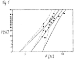
- FIG. 5 shows a diagram in which the frequency P of a deduction of various external contacts against an applied force F is shown.
- a deduction of an external contact falls, for example, a crack of a Jerusalemerressmaschine, a partial detachment of a metallization or a replacement ofmannerWallet réelle of the metallization.
- a device 1 according to FIG. 3 comprising a further contacting 18 in the form of a wire mesh.
- the second metallization 9 was taped with Kapton foil, so that in this area the further contacting 18 was not soldered to the second metallization 9. Subsequently, the non-soldered piece of further contact 18 was attacked during the withdrawal test while exerting various forces. The speed at peeling was 12.5 mm / min.
- the same test was performed with a device 1 in which the first metallization 8 is U-shaped, that is not as in the FIG. 3 the component 1 shown is formed over the entire surface in the form of a rectangle
- the measured values for a full-surface first metallization 8 are represented by circular symbols.
- a Weibull distribution is adjusted, which is represented by dashed lines.
- the measured values for a U-shaped first metallization 8 are represented by the rectangular symbols.
- a Weibull distribution is adjusted, which is represented by solid lines.
- the pull-off average for a full-face first metallization 8 was 5.7 N with a standard deviation of 2.4 N. For a force F of 5.6 N, this was 50% and for a force of 8.2 N was in 90% of cases the external contact 7 deducted.
- the pull-off average for a U-shaped first metallization 8 was 4.1 N with a standard deviation of 1.2 N. For a force F of 4.1 N, 50% and a force of 5.6 N In 90% of cases the external contact 7 had been deducted.
Description
Es wird ein elektrisches Bauelement aufweisend wenigstens eine Metallisierung angegeben. Insbesondere ist die Metallisierung zur Kontaktierung von Innenelektroden des Bauelements vorgesehen. Das elektrische Bauelement ist beispielsweise als Piezoaktor ausgebildet. Weiterhin wird ein Verfahren zur Herstellung einer Kontaktierung eines elektrischen Bauelements angegeben.An electrical component comprising at least one metallization is specified. In particular, the metallization is provided for contacting internal electrodes of the component. The electrical component is formed for example as a piezoelectric actuator. Furthermore, a method for producing a contact of an electrical component is specified.
In der Druckschrift
Es wird ein elektrisches Bauelement angegeben. Beispielsweise ist das Bauelement als Piezoaktor, insbesondere als Piezoaktor zum Betätigen eines Einspritzventils in einem Kraftfahrzeug, ausgebildet. Das Bauelement weist vorzugsweise einen Grundkörper auf. Der Grundkörper weist vorzugsweise Innenelektroden auf. Die Innenelektroden sind beispielsweise als Elektrodenschichten ausgebildet.An electrical component is specified. For example, the component is designed as a piezoelectric actuator, in particular as a piezoelectric actuator for actuating an injection valve in a motor vehicle. The component preferably has a body on. The main body preferably has internal electrodes. The internal electrodes are formed, for example, as electrode layers.
Das Bauelement ist als Vielschichtbauelement ausgebildet, wobei funktionale Schichten und Elektrodenschichten abwechselnd übereinander gestapelt sind. Die funktionalen Schichten sind beispielsweise piezoelektrische Schichten, insbesondere piezokeramische Schichten. Die Innenelektroden erstrecken sich vorzugsweise in Stapelrichtung abwechselnd bis zu einer Außenseite des Grundkörpers und sind von der gegenüberliegenden Außenseite beabstandet. Der Stapel aus Elektrodenschichten und funktionalen Schichten ist vorzugsweise als monolithischer Sinterkörper ausgebildet.The component is designed as a multilayer component, wherein functional layers and electrode layers are alternately stacked on top of each other. The functional layers are, for example, piezoelectric layers, in particular piezoceramic layers. The inner electrodes preferably extend in the stacking direction alternately to an outer side of the main body and are spaced from the opposite outer side. The stack of electrode layers and functional layers is preferably formed as a monolithic sintered body.
Das elektrische Bauelement weist wenigstens einen Außenkontakt aufweisend wenigstens eine Metallisierung auf. Der Außenkontakt ist vorzugsweise zur Kontaktierung von Innenelektroden des Grundkörpers ausgebildet. Die Metallisierung ist vorzugsweise auf einer Außenseite des Grundkörpers angeordnet. Vorzugsweise ist die Metallisierung schichtförmig ausgebildet. Die Metallisierung kontaktiert vorzugsweise jede zweite Innenelektrode. Zur Kontaktierung der weiteren Innenelektroden kann eine weitere Metallisierung vorgesehen sein, die beispielsweise auf einer gegenüberliegenden Außenseite des Grundkörpers angeordnet ist.The electrical component has at least one external contact having at least one metallization. The external contact is preferably designed for contacting internal electrodes of the main body. The metallization is preferably arranged on an outer side of the base body. Preferably, the metallization is layered. The metallization preferably contacts every second inner electrode. For contacting the further inner electrodes, a further metallization may be provided which is arranged, for example, on an opposite outer side of the base body.
Gemäß einem ersten Aspekt der Erfindung weist das elektrische Bauelement einen Außenkontakt mit einer ersten Metallisierung und einer zweiten Metallisierung auf, wobei die zweite Metallisierung auf der ersten Metallisierung angeordnet ist.According to a first aspect of the invention, the electrical component has an external contact with a first metallization and a second metallization, wherein the second metallization is arranged on the first metallization.
Die erste Metallisierung ist vorzugsweise direkt auf einer Außenseite des Grundkörpers angeordnet und vorzugsweise in direktem elektrischen Kontakt mit Innenelektroden des Grundkörpers. Die Metallisierungen dienen vorzugsweise zur elektrischen Kontaktierung der Innenelektroden. Beide Metallisierungen sind als eingebrannte Metallisierungen ausgebildet. Die erste Metallisierung bedeckt die zweite Metallisierung nur teilweise.The first metallization is preferably arranged directly on an outer side of the base body and preferably in direct electrical contact with inner electrodes of the base body. The metallizations are preferably used for electrical contacting of the internal electrodes. Both metallizations are formed as burned metallizations. The first metallization only partially covers the second metallization.
Zur Herstellung einer eingebrannten Metallisierung wird beispielsweise eine metallische Paste auf eine Außenseite des Grundkörpers aufgetragen. Anschließend wird die metallische Paste, beispielsweise bei einer Temperatur im Bereich von 500°C bis 900°C eingebrannt. Erfindungsgemäß wird zur Herstellung der ersten Metallisierung eine erste metallische Paste auf eine Außenseite des Grundkörpers aufgetragen und eingebrannt. Anschließend wird zur Herstellung der zweiten Metallisierung eine zweite metallische Paste auf die erste Metallisierung aufgetragen und eingebrannt. Bei einem derartigen zweistufigen Einbrandprozess der Metallisierungen kann eine Vermischung der Materialien der Metallisierungen besonders gut verhindert werden. Insbesondere kann eine Diffusion von Materialbestandteilen von einer der Metallisierungen in die andere Metallisierung verhindert werden.To produce a baked-on metallization, for example, a metallic paste is applied to an outer side of the base body. Subsequently, the metallic paste, for example, baked at a temperature in the range of 500 ° C to 900 ° C. According to the invention, a first metallic paste is applied to an outside of the base body and baked to produce the first metallization. Subsequently, a second metallic paste is applied to the first metallization and baked to produce the second metallization. In such a two-stage burn-in process of the metallizations, mixing of the materials of the metallizations can be particularly well prevented. In particular, diffusion of material components from one of the metallizations into the other metallization can be prevented.
Gemäß einer Ausführungsform weisen die erste und die zweite Metallisierung eine unterschiedliche Benetzbarkeit mit Lotmaterial auf. Beispielsweise ist das Lotmaterial ein Zinn-Silber-Lot.According to one embodiment, the first and the second metallization have a different wettability with solder material. For example, the solder material is a tin-silver solder.
Durch die unterschiedliche Benetzbarkeit kann erreicht werden, dass ein Kontaktelement, das an wenigstens einer der Metallisierungen befestigt werden soll, ausreichend stark an einer der beiden Metallisierungen befestigt ist und an der anderen Metallisierung weniger gut oder nicht befestigt ist.Due to the different wettability can be achieved that a contact element which is to be attached to at least one of the metallizations, is sufficiently strong attached to one of the two metallizations and is less well or not attached to the other metallization.
Somit kann ein Befestigungsbereich des Kontaktelements durch die Form der Metallisierung mit der höheren Benetzbarkeit bestimmt werden.Thus, a mounting area of the contact element can be determined by the shape of the metallization having the higher wettability.
Vorzugsweise weist die erste Metallisierung eine geringere Benetzbarkeit mit Lotmaterial auf als die zweite Metallisierung. Beispielsweise kann zur Befestigung des Kontaktelements an der ersten Metallisierung das Kontaktelement großflächig mit Lotmaterial versehen sein und auf die Metallisierungen aufgelegt werden. Alternativ kann Lotmaterial großflächig auf die freiliegenden Flächen der Metallisierungen aufgebracht werden. Anschließend wird ein Lötvorgang durchgeführt. Aufgrund der unterschiedlichen Benetzbarkeit der Metallisierungen mit Lotmaterial haftet das Kontaktelement gut an der zweiten Metallisierung und weniger gut oder nicht an der ersten Metallisierung.Preferably, the first metallization has a lower wettability with solder material than the second metallization. For example, to attach the contact element to the first metallization, the contact element can be provided over a large area with solder material and placed on the metallizations. Alternatively, solder material can be applied over a large area to the exposed surfaces of the metallizations. Subsequently, a soldering process is performed. Due to the different wettability of the metallization with solder material, the contact element adheres well to the second metallization and less well or not to the first metallization.
Gemäß einer Ausführungsform weist die erste Metallisierung einen Glasanteil auf und die zweite Metallisierung weist keinen Glasanteil oder einen geringeren Glasanteil als die erste Metallisierung auf.According to one embodiment, the first metallization has a glass component and the second metallization has no glass component or a smaller glass component than the first metalization.
Aufgrund des Glasanteils in der ersten Metallisierung kann eine besonders feste Verbindung der ersten Metallisierung mit dem Grundkörper, insbesondere mit keramischen Schichten des Grundkörpers erzielt werden. Durch den fehlenden oder geringeren Glasanteil der zweiten Metallisierung wird vorzugsweise die Benetzbarkeit der zweiten Metallisierung mit Lotmaterial im Vergleich zur ersten Metallisierung erhöht. Erfindungsgemäß weist die zweite Metallisierung eine kleinere Fläche auf als die erste Metallisierung.Due to the glass content in the first metallization, a particularly firm connection of the first metallization with the base body, in particular with ceramic layers of the base body, can be achieved. Due to the missing or lower glass content of the second metallization, the wettability of the second metallization with solder material is preferably increased in comparison to the first metallization. According to the invention, the second metallization has a smaller area than the first metallization.
Dabei ist mit der Fläche der jeweiligen Metallisierung vorzugsweise die Hauptfläche einer schichtförmigen Metallisierung bezeichnet. Die Hauptfläche verläuft vorzugsweise parallel zur Außenseite des Grundkörpers, auf der die Metallisierungen angeordnet sind.In this case, the main surface of a layered metallization is preferably designated by the surface of the respective metallization. The main surface preferably runs parallel to the outside of the main body on which the metallizations are arranged.
Aufgrund der großen Fläche der ersten Metallisierung kann eine gute Anbindung an den Grundkörper erreicht werden. Augrund der geringeren Fläche der zweiten Metallisierung kann ein Kontaktelement in einem gewünschten, kleineren Bereich befestigt werden, so dass beispielsweise die Flexibilität des Kontaktelements durch den Befestigungsbereich nur wenig beeinträchtigt wird. Dadurch können insbesondere Risse im Grundkörper durch das Kontaktelement überbrückt werden.Due to the large area of the first metallization, a good connection to the main body can be achieved. Due to the smaller area of the second metallization, a contact element can be fastened in a desired, smaller area, so that, for example, the flexibility of the contact element through the attachment area is only slightly impaired. As a result, in particular cracks in the main body can be bridged by the contact element.
Die erste Metallisierung ist beispielsweise vollflächig ausgebildet. Dies bedeutet, dass die erste Metallisierung als durchgehende Fläche ausgebildet ist und keine Aussparungen aufweist. Beispielsweise weist die zweite Metallisierung wenigstens eine Aussparung auf.The first metallization is for example formed over the entire surface. This means that the first metallization is formed as a continuous surface and has no recesses. For example, the second metallization has at least one recess.
Erfindungsgemäß ist die zweite Metallisierung U-förmig ausgebildet. In diesem Fall sind zwei parallel angeordnete Teilbereiche an einem Ende der Teilbereiche durch einen dritten Teilbereich miteinander verbunden.According to the invention, the second metallization is U-shaped. In this case, two partial sections arranged in parallel are connected to one another at one end of the partial areas by a third partial area.
In einer Ausführungsform ist an wenigstens einer der Metallisierungen ein Kontaktelement befestigt. Vorzugsweise ist das Kontaktelement an der zweiten Metallisierung befestigt.In one embodiment, a contact element is attached to at least one of the metallizations. Preferably, the contact element is attached to the second metallization.
Vorzugsweise ist das Kontaktelement flexibel ausgebildet. Auf diese Weise kann das Kontaktelement bei mechanischer Belastung nachgeben ohne zu reißen. Insbesondere kann das Kontaktelement Risse, die im Grundkörper auftreten, überbrücken und so einen zuverlässigen elektrischen Anschluss des Bauelements sicherstellen. Vorzugsweise weist das Kontaktelement wenigstens eine Aussparung auf.Preferably, the contact element is flexible. In this way, the contact element yield under mechanical stress without tearing. In particular, the contact element can bridge cracks that occur in the body, and thus ensure a reliable electrical connection of the device. Preferably, the contact element has at least one recess.
Das Kontaktelement kann eine Netz- oder Gewebestruktur aufweisen. Das Kontaktelement weist beispielsweise eine Vielzahl von Drähten auf. Insbesondere kann das Kontaktelement als Drahtgewebe oder Drahtnetz ausgebildet sein. Alternativ kann das Kontaktelement auch als metallisches Blech ausgebildet sein. In dem metallischen Blech können eine oder mehrere Aussparungen vorgesehen sein, beispielsweise kreisförmige Aussparungen.The contact element may have a mesh or fabric structure. The contact element has, for example, a plurality of wires. In particular, the contact element may be formed as a wire mesh or wire mesh be. Alternatively, the contact element may also be formed as a metallic sheet. In the metallic sheet one or more recesses may be provided, for example circular recesses.
Das Kontaktelement ist vorzugsweise an wenigstens einer der Metallisierungen angelötet. Vorzugsweise ist das Kontaktelement an der zweiten Metallisierung angelötet. Das Kontaktelement kann zusätzlich auch an der ersten Metallisierung angelötet sein. Im Fall, dass die erste Metallisierung eine geringe Benetzbarkeit mit Lotmaterial aufweist, ist das Kontaktelement beispielsweise nicht oder nur mit geringer Haftkraft mit der ersten Metallisierung verlötet.The contact element is preferably soldered to at least one of the metallizations. Preferably, the contact element is soldered to the second metallization. The contact element may additionally be soldered to the first metallization. In the event that the first metallization has a low wettability with solder material, for example, the contact element is not soldered or only with low adhesion to the first metallization.
Vorzugsweise ist wenigstens ein seitlicher Randbereich des Kontaktelements an der zweiten Metallisierung direkt befestigt. Insbesondere steht kein Teil des Randbereichs über die zweite Metallisierung hinaus. Auf diese Weise kann verhindert werden, dass ein unbefestigter Teil des Randbereichs zu einer Beschädigung des Bauelements führt. Beispielsweise ist bei einer rahmenförmigen zweiten Metallisierung das Kontaktelement am Rahmen befestigt und steht nicht seitlich über den Rahmen hinaus. Insbesondere kann bei einer U-förmigen zweiten Metallisierung das Kontaktelement an drei seitlichen Randbereichen an der zweiten Metallisierung befestigt sein. Vorzugsweise steht das Kontaktelement nicht über die erste Metallisierung seitlich über.Preferably, at least one lateral edge region of the contact element is attached directly to the second metallization. In particular, no part of the edge region protrudes beyond the second metallization. In this way it can be prevented that an unpaved part of the edge region leads to damage of the component. For example, in the case of a frame-shaped second metallization, the contact element is fastened to the frame and does not protrude laterally beyond the frame. In particular, in the case of a U-shaped second metallization, the contact element can be fastened to the second metallization at three lateral edge regions. The contact element preferably does not project laterally beyond the first metallization.
In einer Ausführungsform ist am Kontaktelement eine Weiterkontaktierung befestigt. Die Weiterkontaktierung dient vorzugsweise zum elektrischen Anschluss des Bauelements an eine Spannungsquelle. Beispielsweise weist die Weiterkontaktierung einen Draht oder eine Vielzahl von Drähten auf. Vorzugsweise ist die Weiterkontaktierung als Kontaktstift ausgebildet.In one embodiment, a further contact is attached to the contact element. The further contact is preferably used for the electrical connection of the device a voltage source. For example, the further contact has a wire or a plurality of wires. Preferably, the further contact is designed as a contact pin.
Die Weiterkontaktierung ist vorzugsweise nicht oberhalb der zweiten Metallisierung angeordnet. Mit dem Begriff "oberhalb" ist dabei die Richtung der Flächennormale von der mit der zweiten Metallisierung versehenen Außenseite des Grundkörpers bezeichnet. Insbesondere ist die Weiterkontaktierung nicht oberhalb eines Befestigungsbereichs des Kontaktelements an einer der Metallisierungen angeordnet. Auf diese Weise kann die Weiterkontaktierung besonders gut an dem Kontaktelement befestigt werden, ohne dass eine Beschädigung des Bauelements auftritt.The further contacting is preferably not arranged above the second metallization. The term "above" designates the direction of the surface normal of the outside of the base body provided with the second metallization. In particular, the further contacting is not arranged above a fastening region of the contact element on one of the metallizations. In this way, the further contact can be attached particularly well to the contact element, without damaging the device occurs.
Beispielsweise ist die Weiterkontaktierung am Kontaktelement angeschweißt. Die Weiterkontaktierung kann beim Befestigungsschritt an das Kontaktelement angedrückt werden. Wenn das Kontaktelement in diesem Bereich nicht direkt an einer Metallisierung befestigt ist, kann das Kontaktelement beispielsweise nachgeben, wodurch ein guter Kontakt des Kontaktelements mit der Weiterkontaktierung erzielt werden kann. Weiterhin wird in diesem Fall beim Befestigungsschritt, insbesondere einem Schweiß- oder Lötvorgang, die Grundmetallisierung nicht beschädigt.For example, the further contact is welded to the contact element. The further contact can be pressed against the contact element during the fastening step. If the contact element in this area is not fastened directly to a metallization, the contact element can yield, for example, whereby a good contact of the contact element with the further contact can be achieved. Furthermore, in this case, in the fastening step, in particular a welding or soldering, the base metallization is not damaged.
Die Weiterkontaktierung ist vorzugsweise zumindest teilweise oberhalb der ersten Metallisierung angeordnet. Beispielsweise erstreckt sich die Weiterkontaktierung bei einer U-förmigen Ausgestaltung der zweiten Metallisierung durch die Öffnung des U-förmigen Bereichs in das Innere des U-förmigen Bereichs hinein.The further contacting is preferably arranged at least partially above the first metallization. For example, in the case of a U-shaped configuration of the second metallization, the further contacting extends through the opening of the U-shaped region into the interior of the U-shaped region.
Gemäß einem weiteren Aspekt der Erfindung wird ein elektrisches Bauelement mit wenigstens einem Außenkontakt aufweisend wenigstens eine Metallisierung angegeben, wobei die Metallisierung rahmenförmig ausgebildet ist, wobei die Rahmenform der Metallisierung eine Öffnung aufweist, so dass die Rahmenform U-förmig ausgebildet ist.According to a further aspect of the invention, an electrical component with at least one external contact having at least one metallization is specified, wherein the metallization is designed as a frame, wherein the frame shape of the metallization has an opening, so that the frame shape is U-shaped.
In einer Ausführungsform ist an der rahmenförmigen Metallisierung ein Kontaktelement wie oben beschrieben befestigt. Vorzugsweise ist wenigstens ein seitlicher Randbereich des Kontaktelements am Rahmen direkt befestigt. Zudem kann eine Weiterkontaktierung, insbesondere in Form eines Kontaktstifts am Kontaktelement befestigt sein.In one embodiment, a contact element is attached to the frame-shaped metallization as described above. Preferably, at least one lateral edge region of the contact element is fastened directly to the frame. In addition, a further contact, in particular be attached in the form of a contact pin on the contact element.
Gemäß einem weiteren Aspekt der Erfindung wird ein Verfahren zur Herstellung einer elektrischen Kontaktierung eines elektrischen Bauelements angegeben. Es wird ein Grundkörper eines elektrischen Bauelements bereitgestellt und eine erste metallische Paste auf einer Außenseite des Grundkörpers aufgebracht. Anschließend wird die erste metallische Paste zur Ausbildung einer ersten Metallisierung eingebrannt. Danach wird eine zweite metallische Paste auf die erste Metallisierung aufgebracht und anschließend wird die zweite metallische Paste eingebrannt. Durch das Verfahren werden die oben beschriebenen Bauelemente hergestellt, wobei die im Verfahren verwendeten Bestandteile alle funktionellen und strukturellen Eigenschaften der Bestandteile der oben beschriebenen Bauelemente aufweisen.According to a further aspect of the invention, a method for producing an electrical contacting of an electrical component is specified. A main body of an electrical component is provided and a first metallic paste is applied to an outer side of the main body. Subsequently, the first metallic paste is baked to form a first metallization. Thereafter, a second metallic paste is applied to the first metallization and then the second metallic paste is baked. The method produces the components described above, wherein the components used in the method have all the functional and structural properties of the components of the components described above.
An wenigstens einer der Metallisierungen kann ein Kontaktelement befestigt, insbesondere angelötet werden. Dazu wird das Kontaktelement beispielsweise großzügig mit Lotmaterial beschichtet. Die erste und zweite Metallisierung können eine unterschiedliche Benetzbarkeit mit Lotmaterial aufweisen. Auf diese Weise kann erreicht werden, dass das Kontaktelement nur an einer der Metallisierungen befestigt wird und an der anderen Metallisierung nicht oder wenig gut befestigt wird. Weiterhin kann an dem Kontaktelement eine Weiterkontaktierung wie oben beschrieben befestigt werden, beispielsweise angeschweißt werden.At least one of the metallizations, a contact element attached, in particular soldered. For this purpose, the contact element, for example, generously coated with solder material. The first and second metallizations may have different wettability with solder material. In this way it can be achieved that the contact element is attached only to one of the metallizations and not or only slightly on the other metallization is attached. Furthermore, a further contact can be attached to the contact element as described above, for example, welded.
Im Folgenden werden die hier beschriebenen Gegenstände anhand von schematischen und nicht maßstabsgetreuen Ausführungsbeispielen näher erläutert. Es zeigen:
Figur 1- eine Aufsicht auf ein elektrisches Bauelement,
Figur 2- einen Querschnitt des Bauelements aus
Figur 1 , Figur 3- eine Aufsicht auf ein elektrisches Bauelement aufweisend ein Kontaktelement,
- Figuren 4A, 4B, 4C, 4D
- Verfahrensschritte bei der Herstellung einer Kontaktierung eines elektrischen Bauelements,
Figur 5- in einem Diagramm die Häufigkeit eines Abzugs von Außenkontakten in Abhängigkeit von einer ausgeübten Kraft.
- FIG. 1
- a view of an electrical component,
- FIG. 2
- a cross section of the device
FIG. 1 . - FIG. 3
- a plan view of an electrical component having a contact element,
- FIGS. 4A, 4B, 4C, 4D
- Method steps in the production of a contacting of an electrical component,
- FIG. 5
- in a diagram, the frequency of a withdrawal of external contacts as a function of an applied force.
Vorzugsweise verweisen in den folgenden Figuren gleiche Bezugszeichen auf funktionell oder strukturell entsprechende Teile der verschiedenen Ausführungsformen.Preferably, like reference numerals refer to functionally or structurally corresponding parts of the various embodiments in the following figures.
Das elektrische Bauelement 1 ist vorzugsweise ein piezoelektrisches Bauelement, insbesondere ein Piezoaktor. Das Bauelement 1 ist als Vielschichtbauelement ausgebildet.The
Das Bauelement 1 weist einen Grundkörper 2 auf, in dem erste und zweite Innenelektroden 3, 4 und funktionale Schichten 5 entlang einer Stapelrichtung S abwechselnd übereinander gestapelt sind.The
Die Innenelektroden 3, 4 erstrecken sich abwechselnd bis zu einer Außenseite 6 der Grundkörpers 2 und sind von einer gegenüberliegenden Außenseite (nicht abgebildet) beabstandet. Beispielsweise enthalten die Innenelektroden 3, 4 Kupfer, Silber, oder Silber-Palladium.The
Die funktionalen Schichten 5 sind beispielsweise als dielektrische Schichten, insbesondere als piezoelektrische Schichten, ausgebildet. Die funktionalen Schichten 5 können aus einem keramischen Material gebildet sein, insbesondere als piezokeramische Schichten ausgebildet sein. Vorzugsweise dehnt sich das Bauelement 1 beim Anlegen einer Spannung zwischen die Innenelektroden 3, 4 aus. Die Ausdehnung erfolgt beispielsweise in Stapelrichtung S.The
Zur Kontaktierung der ersten Innenelektroden 3 ist ein Außenkontakt 7 auf einer Außenseite 6 des Grundkörpers 2 angeordnet. Der Außenkontakt 7 weist eine erste Metallisierung 8 und eine zweite Metallisierung 9 auf. Die erste Metallisierung 8 ist in direktem Kontakt mit den funktionalen Schichten 5 und den ersten Innenelektroden 3. Die zweite Metallisierung 9 ist auf der ersten Metallisierung 8 angeordnet und ist in direktem Kontakt mit der ersten Metallisierung 8. Die Metallisierungen 8, 9 sind schichtförmig ausgebildet. Die zweite Metallisierung 9 bedeckt die Außenseite der ersten Metallisierung 8, auf der sie angeordnet ist, d.h. die vom Grundkörper 2 abgewandte Außenseite der ersten Metallisierung 8, nur teilweise und lässt Teilbereiche der Außenseite der ersten Metallisierung 8 unbedeckt.For contacting the first
Beide Metallisierungen 8, 9 sind als Einbrandmetallisierungen ausgebildet. Insbesondere sind die Metallisierungen 8, 9 durch Auftragen und Einbrennen einer metallischen Paste hergestellt. Vorzugsweise wird zuerst die erste Metallisierung 8, beispielsweise durch Siebdrucken, aufgebracht und eingebrannt. Anschließend wird die zweite Metallisierung 9, beispielsweise durch Siebdrucken, aufgebracht und eingebrannt.Both
Beide Metallisierungen 8, 9 enthalten ein Metall. Vorzugsweise enthält wenigstens eine der Metallisierungen 8, 9 Kupfer. Alternativ oder zusätzlich können die Metallisierungen 8, 9 Silber oder Silber-Palladium enthalten. Die Metallisierungen 8, 9 können auch unterschiedliche Metalle enthalten, Beispielsweise kann eine der Metallisierungen Kupfer und die andere Metallisierung Silber enthalten.Both
Die erste Metallisierung 8 enthält einen Glasanteil, insbesondere eine Glasfritte. Der Glasanteil gewährleistet vorzugsweise die Haftfestigkeit der Metallisierung 8 auf der Außenseite 6 der Grundkörpers 2, beispielsweise an einem keramischen Material des Grundkörpers 2. Vorzugsweise liegt der Glasanteil in der ersten Metallisierung 8 zwischen 3 und 10 Gewichtsprozent (Gew.-%). Beispielsweise liegt der Glasanteil bei 6 Gew.-%. Der Glasanteil in der ersten Metallisierung 8 hat zur Folge, dass die Benetzbarkeit der ersten Metallisierung 8 mit einem Lotmaterial gering ist.The
Die zweite Metallisierung 9 weist keinen Glasanteil auf oder weist einen geringeren Glasanteil auf als die erste Metallisierung 8 auf. Beim Einbrennen der zweiten Metallisierung 9 kann allerdings ein geringer Glasanteil aus der ersten Metallisierung 8 in die zweite Metallisierung 9 diffundieren, so dass, auch wenn zur Herstellung der zweiten Metallisierung 9 eine Paste ohne Glasanteil verwendet wird, ein geringer Glasanteil nach dem Einbrennen in der zweiten Metallisierung 9 vorhanden sein kann. Durch ein zweistufiges Einbrennen der Metallisierungen 8, 9 kann eine derartige Diffusion ganz oder weitgehend verhindert werden. Die erste Metallisierung 8 kann eine höhere Porosität aufweisen als die zweite Metallisierung 9.The
Beispielsweise besteht die zweite Metallisierung 9 aus einem Metall. Die zweite Metallisierung 9 weist aufgrund des fehlenden oder geringen Glasanteils eine gute Benetzbarkeit mit einem Lotmaterial auf.For example, the
Die erste Metallisierung 8 ist in Form einer rechteckigen Fläche ausgebildet. Insbesondere weist die erste Metallisierung 8 keine Aussparungen auf, ist also vollflächig ausgebildet.The
Die zweite Metallisierung 9 weist zwei streifenförmige Teilbereiche 10, 11 auf, die parallel zueinander verlaufen. Die Teilbereiche 10, 11 verlaufen in Stapelrichtung S. Zwischen den Teilbereichen 10, 11 weist die zweite Metallisierung 9 eine Aussparung 12 auf, durch die die erste Metallisierung 8 zu sehen ist. Die zwei Teilbereiche 10, 11 sind durch einen dritten Teilbereich 13 miteinander verbunden. Der dritte Teilbereich 13 verläuft senkrecht zur Stapelrichtung S. Die zweite Metallisierung 9 ist insgesamt U-förmig ausgebildet. Insbesondere ist die zweite Metallisierung 9 rahmenförmig ausgebildet, wobei eine Öffnung 17 in der Rahmenform vorgesehen ist.The
Die erste Metallisierung 8 weist in eingebranntem Zustand vorzugsweise eine Dicke d1 (siehe
Die Fläche der ersten Metallisierung 8 ist größer als die Fläche der zweiten Metallisierung 9. Durch die große Fläche der ersten Metallisierung 8 kann eine gute Haftfestigkeit des Außenkontakts 7 an der Außenseite 6 gewährleistet werden. Durch die kleinere Fläche der zweiten Metallisierung 9 kann ein Kontaktelement in einem kleineren Befestigungsbereich an der zweiten Metallisierung 9 befestigt werden. Durch den unterschiedlichen Grad der Benetzbarkeit der ersten und zweiten Metallisierung 8, 9 kann ein Kontaktelement auf einfache Weise nur an der zweiten Metallisierung 8 und nicht, oder nur in geringem Grad, an der ersten Metallisierung 9 befestigt werden. Dies erlaubt beispielsweise eine Befestigung des Kontaktelements nur in durch die zweite Metallisierung 9 definierten Befestigungsbereichen.The area of the
Das elektrische Bauelement 1 ist wie das in den
Das Kontaktelement 14 ist an der zweiten Metallisierung 9 angelötet. Durch die unterschiedliche Benetzbarkeit der ersten und zweiten Metallisierung 8, 9 mit einem Lotmaterial haftet das Lotmaterial gut an der zweiten Metallisierung 9, aber nur schlecht oder überhaupt nicht an der ersten Metallisierung 8. Somit wird ein Befestigungsbereich 15, in dem das Kontaktelement 14 mit der darunter liegenden Metallisierung 8, 9 verlötet ist, durch die Geometrie der zweiten Metallisierung 9 bestimmt. Somit kann zur Verlötung des Kontaktelements 14 im Kontaktbereich 15 ein Lotmaterial großflächig auf dem Kontaktelement 14 oder den Metallisierungen 8, 9 aufgebracht sein. Aufgrund der guten Benetzbarkeit der zweiten Metallisierung 9 wird das Kontaktelement 14 mit der zweiten Metallisierung 9 durch das Lotmaterial fest verbunden. Aufgrund der schlechten Benetzbarkeit der ersten Metallisierung 8 wird das Kontaktelement 14 nicht oder nur mit geringer Haftfestigkeit mit der ersten Metallisierung 8 verbunden. Somit kann das Kontaktelement 14 auf einfache Weise nur in einem gewünschten Befestigungsbereich 15 befestigt werden. Insbesondere kann das Kontaktelement 14 nur partiell, d.h. nur in Teilen seiner Außenfläche befestigt sein, während in einem Bereich geringer Haftfestigkeit 16 das Kontaktelement 14 nicht oder nur mit geringer Haftfestigkeit 16 mit dem Grundkörper 2 verbunden ist. Dies ermöglicht beispielsweise die elektrische Überbrückung von Rissen im Grundkörper 2, die während einer Polarisation des Bauelements 1 oder im Betrieb auftreten können. Vorzugsweise ist das Kontaktelement 14 flexibel ausgebildet, so dass es beim Auftreten von mechanischen Spannungen, die z. B. durch einen Riss im Grundkörper 2 erzeugt werden, gedehnt wird ohne zu reißen.The
Zum elektrischen Anschluss des Außenkontakts 7 kann eine Weiterkontaktierung 18, beispielsweise ein Kontaktstift, am Außenkontakt 7 befestigt sein (siehe
Die
Gemäß
Beispielsweise findet der Einbrandschritt bei einer Temperatur von 760 °C in einer N2-Atmosphäre statt.For example, the burn-in step takes place at a temperature of 760 ° C. in an N 2 atmosphere.
Auf die so erhaltene erste Metallisierung 8 wird gemäß
Auf die erhaltene zweite Metallisierung 9 werden optional eine oder mehrere weitere, dünne metallische Schichten aufgebracht. Diese Schichten können zum Schutz der zweiten Metallisierung 9, insbesondere bei einer Kupfer aufweisenden zweiten Metallisierung 9, ausgebildet sein. Beispielsweise werden die Schichten aufgesputtert. Beispielsweise kann eine Kupferschicht und darüber eine Silberschicht auf die zweite Metallisierung 9 aufgebracht werden. Die Kupferschicht ist beispielsweise 0,3 µm dick und die Silberschicht 0,4 µm dick. Die Silberschicht löst sich vorzugsweise in einem Lotmaterial. Durch Aufbringen der weiteren Schichten kann die Lötbarkeit der zweiten Metallisierung 9 verbessert werden.One or more further, thin metallic layers are optionally applied to the obtained
Gemäß
Bei der Verlötung des Kontaktelements 14 wird das Kontaktelement 14 vorzugsweise an den Grundkörper 2 angepresst. Dadurch, dass die zweite Metallisierung 9 auf der ersten Metallisierung 8 angeordnet ist und somit eine Stufe zwischen der ersten und zweiten Metallisierung 8, 9 ausgebildet ist, ist der Anpressdruck auf der zweiten Metallisierung 9 höher als auf der ersten Metallisierung 8. Durch den unterschiedlichen Anpressdruck wird die unterschiedliche Haftfestigkeit des Kontaktelements auf der zweiten Metallisierung 9 zusätzlich unterstützt.When soldering the
Die äußere geometrische Abmessung des Kontaktelements 14 ist vorzugsweise etwas geringer als die äußere Abmessung der zweiten Metallisierung 9. Somit steht das Kontaktelement 14 nicht über die zweite Metallisierung 9 seitlich über. Insbesondere sind seitliche Randbereiche des Kontaktelements 14 mit der zweiten Metallisierung 9 verlötet. Auf diese Weise kann die Zuverlässigkeit des Bauelements 1 erhöht werden. Insbesondere kann verhindert werden, dass überstehende Bereiche des Kontaktelements 14 beschädigt werden, zur Ablösung des Kontaktelements 14 führen oder zu einem Kurzschluss führen.The outer geometric dimension of the
Gemäß
Die Weiterkontaktierung 18 erstreckt sich über die Öffnung 17 der zweiten Metallisierung 9 in einen mittigen Bereich oberhalb der U-förmigen zweiten Metallisierung 9 hinein. Bei einer derartigen Anordnung der Weiterkontaktierung 18 kann die Weiterkontaktierung 18 besonders zuverlässig an dem Kontaktelement 16 befestigt werden. Bei dem Schweißvorgang kann die Weiterkontaktierung 18 an das Kontaktelement 14 angedrückt werden, wobei durch die Nachgiebigkeit des Kontaktelements 14 im Bereich geringer Haftfestigkeit 16 ein guter Kontakt zwischen der Weiterkontaktierung 18 und dem Kontaktelement 14 hergestellt werden kann. Weiterhin ist bei einer Anordnung der Weiterkontaktierung 18 derart, dass der Kontaktstift nicht oberhalb der zweiten Metallisierung 9 angeordnet ist, die Gefahr einer Beschädigung des Außenkontakts 7 beim Schweißvorgang verringert. Darüber hinaus beeinträchtigt eine derart angeordnete Weiterkontaktierung 18 eine Ausdehnung des Bauelements 1 nicht oder nur wenig.The further contact 18 extends through the
Für den Abzugstest wurde ein Bauelement 1 gemäß
Zum Vergleich wurde derselbe Test mit einem Bauelement 1 durchgeführt, bei dem die erste Metallisierung 8 U-förmig ausgebildet ist, also nicht wie bei dem in
Insgesamt lässt sich aus dem Diagramm ablesen, dass bei einer vollflächig aufgebrachten ersten Metallisierung 8 die Abzugskräfte um ca. 40 % gegenüber einer U-förmig aufgebrachten ersten Metallisierung erhöht sind. Der Mittelwert für die Abzugskraft lag bei einer vollflächigen ersten Metallisierung 8 bei 5,7 N mit einer Standardabweichung von 2,4 N. Bei einer Kraft F von 5,6 N war in 50 % und bei einer Kraft von 8,2 N war in 90 % der Fälle der Außenkontakt 7 abgezogen. Der Mittelwert für die Abzugskraft lag bei einer U-förmigen ersten Metallisierung 8 bei 4,1 N mit einer Standardabweichung von 1,2 N. Bei einer Kraft F von 4,1 N war in 50 % und bei einer Kraft von 5,6 N war in 90 % der Fälle der Außenkontakt 7 abgezogen.Overall, it can be read from the diagram that with a full-surface applied
- 11
- elektrisches Bauelementelectrical component
- 22
- Grundkörperbody
- 33
- erste Innenelektrodefirst inner electrode
- 44
- zweite Innenelektrodesecond inner electrode
- 55
- dielektrische Schichtdielectric layer
- 66
- Außenseiteoutside
- 77
- Außenkontaktoutside Contact
- 88th
- erste Metallisierungfirst metallization
- 99
- zweite Metallisierungsecond metallization
- 1010
- erster Teilbereichfirst subarea
- 1111
- zweiter Teilbereichsecond subarea
- 1212
- Aussparung in zweiter MetallisierungRecess in second metallization
- 1313
- dritter Teilbereichthird subarea
- 1414
- Kontaktelementcontact element
- 1515
- Befestigungsbereichfastening area
- 1616
- Bereich geringer HaftfestigkeitLow adhesion area
- 1717
- Öffnungopening
- 1818
- Weiterkontaktierungfurther contact
- 1919
- erste metallische Pastefirst metallic paste
- 2020
- zweite metallische Pastesecond metallic paste
- SS
- Stapelrichtungstacking direction
- d1 d 1
- Dicke der ersten MetallisierungThickness of the first metallization
- d2 d 2
- Dicke der zweiten MetallisierungThickness of the second metallization
- PP
- Häufigkeit eines Abzugs eines AußenkontaktsFrequency of deduction of an external contact
- FF
- Kraftforce
Claims (15)
- Electrical component (1), which is embodied as a multilayer component having functional layers (5) and internal electrodes (3, 4) lying therebetween, comprising at least one external contact (7) having a first metallization (8) and a second metallization (9), which is arranged on the first metallization (8), wherein the first and second metallizations (8, 9) are fired, wherein the second metallization (9) only partly covers the first metallization (8), characterized in that the second metallization (9) is embodied in a U-shaped fashion.
- Electrical component according to Claim 1, wherein the first and second electrical components (8, 9) have a different wettability with solder material.
- Electrical component according to either of the preceding claims, wherein the first metallization (8) has a glass portion and wherein the second metallization (9) has no glass portion or a smaller glass portion than the first metallization (8).
- Electrical component according to any of the preceding claims, wherein the second metallization (9) has at least one cutout (12).
- Electrical component according to Claim 4, wherein the first metallization (8) can be seen in the cutout (12) .
- Electrical component according to any of the preceding claims, wherein the first metallization (8) is embodied over the whole area.
- Electrical component according to any of the preceding claims, wherein a contact element (14) is fixed to the second metallization (9).
- Electrical component according to Claim 7, wherein the contact element (14) is soldered.
- Electrical component according to either of Claims 7 and 8, wherein the contact element (14) has a fabric structure.
- Electrical component according to any of Claims 7 to 9, having a further contact-connection (18), which is fixed to the contact element (14).
- Electrical component according to Claim 10, wherein the further contact-connection (18) is not arranged above the second metallization (9).
- Electrical component according to either of Claims 10 and 11, wherein the further contact-connection (18) extends above an opening (17) of the U-shape into the interior of the U-shape.
- Electrical component according to any of Claims 10 to 12, wherein the further contact-connection (18) is embodied as a contact pin.
- Electrical component according to one of the preceding claims, which is embodied as a piezoactuator.
- Method for establishing electrical contact with an electrical component according to any of the preceding claims, having the steps ofA) providing a main body (2) of the electrical component (1) and applying a first metallic paste (19) on an outer side (6) of the main body (2),B) firing the first metallic paste (19) to form the first metallization (8),C) applying a second metallic paste (20) to the first metallization (8),D) firing the second metallic paste (20) to form the second metallization (9).
Applications Claiming Priority (2)
| Application Number | Priority Date | Filing Date | Title |
|---|---|---|---|
| DE102012109250.8A DE102012109250B4 (en) | 2012-09-28 | 2012-09-28 | Electrical component and method for producing contacting of an electrical component |
| PCT/EP2013/068633 WO2014048713A2 (en) | 2012-09-28 | 2013-09-09 | Electrical component and method for establishing contact with an electrical component |
Publications (2)
| Publication Number | Publication Date |
|---|---|
| EP2901504A2 EP2901504A2 (en) | 2015-08-05 |
| EP2901504B1 true EP2901504B1 (en) | 2018-08-15 |
Family
ID=49165729
Family Applications (1)
| Application Number | Title | Priority Date | Filing Date |
|---|---|---|---|
| EP13762093.6A Active EP2901504B1 (en) | 2012-09-28 | 2013-09-09 | Electrical component and method for establishing contact with an electrical component |
Country Status (6)
| Country | Link |
|---|---|
| US (1) | US9613773B2 (en) |
| EP (1) | EP2901504B1 (en) |
| JP (2) | JP6486273B2 (en) |
| CN (1) | CN104662685B (en) |
| DE (1) | DE102012109250B4 (en) |
| WO (1) | WO2014048713A2 (en) |
Families Citing this family (2)
| Publication number | Priority date | Publication date | Assignee | Title |
|---|---|---|---|---|
| US10658565B2 (en) * | 2016-08-29 | 2020-05-19 | The Boeing Company | Actuator assemblies, mechanical assemblies including the actuator assemblies, and methods of fabricating the same |
| US11296272B2 (en) * | 2017-07-20 | 2022-04-05 | Taiyo Yuden Co., Ltd. | Multilayer piezoelectric element, piezoelectric vibration apparatus, and electronic device |
Family Cites Families (24)
| Publication number | Priority date | Publication date | Assignee | Title |
|---|---|---|---|---|
| JPS63120450A (en) * | 1986-11-10 | 1988-05-24 | Shinko Electric Ind Co Ltd | Manufacture of semiconductor device and lead frame used therefor |
| DE19648545B4 (en) | 1996-11-25 | 2009-05-07 | Ceramtec Ag | Monolithic multilayer actuator with external electrodes |
| DE19917728A1 (en) * | 1999-04-20 | 2000-10-26 | Bosch Gmbh Robert | Piezoelectric actuator particularly for operating control valves or injection valves in vehicles, has additional planar electrode strip adjacent actuator body with double comb-type legs |
| US20010026114A1 (en) * | 2000-03-29 | 2001-10-04 | Tokin Ceramics Corporation | Multilayer piezoelectric actuator with electrodes reinforced in conductivity |
| US20010033125A1 (en) * | 2000-04-20 | 2001-10-25 | Tokin Corporation | Multilayer piezoelectric actuator device having a conductive member attached to an external electrode thereof |
| JP3964184B2 (en) * | 2000-12-28 | 2007-08-22 | 株式会社デンソー | Multilayer piezoelectric actuator |
| DE10327902A1 (en) | 2002-07-19 | 2004-06-24 | Ceramtec Ag Innovative Ceramic Engineering | External electrode on a piezoceramic multilayer actuator |
| DE10356961A1 (en) * | 2003-12-05 | 2005-06-30 | Robert Bosch Gmbh | Actuator module for fuel injection valves has pin with good heat conductivity characteristics, which transfers the heat away from the actuator |
| US7385337B2 (en) * | 2004-06-18 | 2008-06-10 | Tdk Corporation | Multilayer piezoelectric element |
| JP4706209B2 (en) * | 2004-08-30 | 2011-06-22 | 株式会社デンソー | Multilayer piezoelectric element, manufacturing method thereof, and conductive adhesive |
| JP2006303045A (en) * | 2005-04-18 | 2006-11-02 | Denso Corp | Laminated piezoelectric element |
| EP2003707B1 (en) | 2006-03-31 | 2012-03-14 | Murata Manufacturing Co. Ltd. | Piezoelectric actuator |
| JP5087914B2 (en) * | 2006-12-06 | 2012-12-05 | Tdk株式会社 | Multilayer piezoelectric element |
| JP2008243924A (en) * | 2007-03-26 | 2008-10-09 | Ngk Spark Plug Co Ltd | Laminated type piezoelectric actuator element and laminated type piezoelectric actuator |
| JP2009123750A (en) * | 2007-11-12 | 2009-06-04 | Denso Corp | Stacked piezoelectric device |
| CN101978518A (en) | 2008-03-21 | 2011-02-16 | 日本碍子株式会社 | Piezoelectric/electrostrictive element and manufacturing method thereof |
| CN101978522A (en) * | 2008-04-11 | 2011-02-16 | 株式会社村田制作所 | Multilayer piezoelectric actuator |
| DE102008062021A1 (en) | 2008-08-18 | 2010-03-04 | Epcos Ag | Piezo actuator in multilayer construction |
| US20110168806A1 (en) * | 2008-08-26 | 2011-07-14 | Kyocera Corporation | Multi-Layer Piezoelectric Element, and Injection Device and Fuel Injection System Using the Same |
| CN102449792B (en) | 2009-05-26 | 2014-05-14 | 京瓷株式会社 | Laminated piezoelectric element, jetting device using same, and fuel jetting system |
| WO2011013689A1 (en) * | 2009-07-28 | 2011-02-03 | 京セラ株式会社 | Stacked piezoelectric element, injection device using same, and fuel injection system |
| CN103098251B (en) * | 2010-10-28 | 2015-04-01 | 京瓷株式会社 | Laminated piezoelectric element, injection device using same, and fuel injection system |
| WO2014069452A1 (en) * | 2012-10-29 | 2014-05-08 | 京セラ株式会社 | Multilayered piezo element, as well as piezo actuator, injection apparatus, and fuel injection system provided with said element |
| EP3101701B1 (en) * | 2014-01-30 | 2019-09-11 | Kyocera Corporation | Laminated piezoelectric element, and injection device and fuel-injection system containing said laminated piezoelectric element |
-
2012
- 2012-09-28 DE DE102012109250.8A patent/DE102012109250B4/en active Active
-
2013
- 2013-09-09 JP JP2015533517A patent/JP6486273B2/en active Active
- 2013-09-09 WO PCT/EP2013/068633 patent/WO2014048713A2/en active Application Filing
- 2013-09-09 US US14/431,726 patent/US9613773B2/en active Active
- 2013-09-09 EP EP13762093.6A patent/EP2901504B1/en active Active
- 2013-09-09 CN CN201380050759.4A patent/CN104662685B/en active Active
-
2017
- 2017-07-14 JP JP2017138300A patent/JP6629796B2/en active Active
Non-Patent Citations (1)
| Title |
|---|
| None * |
Also Published As
| Publication number | Publication date |
|---|---|
| US9613773B2 (en) | 2017-04-04 |
| CN104662685B (en) | 2017-08-15 |
| JP6486273B2 (en) | 2019-03-20 |
| WO2014048713A3 (en) | 2014-06-05 |
| JP2017201714A (en) | 2017-11-09 |
| JP2015531548A (en) | 2015-11-02 |
| CN104662685A (en) | 2015-05-27 |
| US20150255237A1 (en) | 2015-09-10 |
| DE102012109250A1 (en) | 2014-04-03 |
| WO2014048713A2 (en) | 2014-04-03 |
| JP6629796B2 (en) | 2020-01-15 |
| DE102012109250B4 (en) | 2020-07-16 |
| EP2901504A2 (en) | 2015-08-05 |
Similar Documents
| Publication | Publication Date | Title |
|---|---|---|
| EP2316142B1 (en) | Piezoactuator in multi-layered construction | |
| EP3371565B1 (en) | Sensor element and method for producing a sensor element | |
| EP2057647B1 (en) | Component assembly | |
| EP1761936B1 (en) | Electrical multi-layered component having a reliable soldering contact | |
| EP2011170B1 (en) | Method for the production of a piezo actuator | |
| EP2345095B1 (en) | Piezoelectric actuator of multilayer design and method for fastening an outer electrode in a piezoelectric actuator | |
| DE3638286A1 (en) | Electrical component, made of ceramic and having multilayer metallisation, and a method for its production | |
| DE102004006778A1 (en) | Stacked piezoelectric device | |
| EP2901504B1 (en) | Electrical component and method for establishing contact with an electrical component | |
| EP1774543B1 (en) | Electric component and method for the production of an electric component | |
| DE102010022925B4 (en) | Piezoelectric multilayer component and method for forming an outer electrode in a piezoelectric multilayer component | |
| EP3033756B1 (en) | Method for producing a multilayer component comprising an external contact | |
| EP1714328A2 (en) | Piezo actuator and a method for the production thereof | |
| DE19635276C2 (en) | Electro-ceramic multilayer component and method for its production | |
| DE102018123594B4 (en) | Process for the production of a ceramic component | |
| DE102012105517B4 (en) | Multilayer component with an external contact and method for producing a multilayer component with an external contact | |
| DE102014217938B4 (en) | electronic component | |
| DE102012110556B4 (en) | Multi-layer component and method for its production | |
| DE19634488A1 (en) | Electrically conductive ceramic SMD component | |
| WO2020064403A1 (en) | Ceramic component and method for producing the ceramic component |
Legal Events
| Date | Code | Title | Description |
|---|---|---|---|
| PUAI | Public reference made under article 153(3) epc to a published international application that has entered the european phase |
Free format text: ORIGINAL CODE: 0009012 |
|
| 17P | Request for examination filed |
Effective date: 20150209 |
|
| AK | Designated contracting states |
Kind code of ref document: A2 Designated state(s): AL AT BE BG CH CY CZ DE DK EE ES FI FR GB GR HR HU IE IS IT LI LT LU LV MC MK MT NL NO PL PT RO RS SE SI SK SM TR |
|
| AX | Request for extension of the european patent |
Extension state: BA ME |
|
| DAX | Request for extension of the european patent (deleted) | ||
| RAP1 | Party data changed (applicant data changed or rights of an application transferred) |
Owner name: EPCOS AG |
|
| GRAP | Despatch of communication of intention to grant a patent |
Free format text: ORIGINAL CODE: EPIDOSNIGR1 |
|
| INTG | Intention to grant announced |
Effective date: 20180508 |
|
| GRAS | Grant fee paid |
Free format text: ORIGINAL CODE: EPIDOSNIGR3 |
|
| GRAA | (expected) grant |
Free format text: ORIGINAL CODE: 0009210 |
|
| AK | Designated contracting states |
Kind code of ref document: B1 Designated state(s): AL AT BE BG CH CY CZ DE DK EE ES FI FR GB GR HR HU IE IS IT LI LT LU LV MC MK MT NL NO PL PT RO RS SE SI SK SM TR |
|
| REG | Reference to a national code |
Ref country code: CH Ref legal event code: EP Ref country code: GB Ref legal event code: FG4D Free format text: NOT ENGLISH Ref country code: AT Ref legal event code: REF Ref document number: 1030779 Country of ref document: AT Kind code of ref document: T Effective date: 20180815 |
|
| REG | Reference to a national code |
Ref country code: IE Ref legal event code: FG4D Free format text: LANGUAGE OF EP DOCUMENT: GERMAN |
|
| REG | Reference to a national code |
Ref country code: DE Ref legal event code: R096 Ref document number: 502013010879 Country of ref document: DE |
|
| REG | Reference to a national code |
Ref country code: DE Ref legal event code: R082 Ref document number: 502013010879 Country of ref document: DE Representative=s name: EPPING HERMANN FISCHER PATENTANWALTSGESELLSCHA, DE Ref country code: DE Ref legal event code: R081 Ref document number: 502013010879 Country of ref document: DE Owner name: TDK ELECTRONICS AG, DE Free format text: FORMER OWNER: EPCOS AG, 81671 MUENCHEN, DE |
|
| REG | Reference to a national code |
Ref country code: NL Ref legal event code: MP Effective date: 20180815 |
|
| REG | Reference to a national code |
Ref country code: LT Ref legal event code: MG4D |
|
| PG25 | Lapsed in a contracting state [announced via postgrant information from national office to epo] |
Ref country code: GR Free format text: LAPSE BECAUSE OF FAILURE TO SUBMIT A TRANSLATION OF THE DESCRIPTION OR TO PAY THE FEE WITHIN THE PRESCRIBED TIME-LIMIT Effective date: 20181116 Ref country code: SE Free format text: LAPSE BECAUSE OF FAILURE TO SUBMIT A TRANSLATION OF THE DESCRIPTION OR TO PAY THE FEE WITHIN THE PRESCRIBED TIME-LIMIT Effective date: 20180815 Ref country code: BG Free format text: LAPSE BECAUSE OF FAILURE TO SUBMIT A TRANSLATION OF THE DESCRIPTION OR TO PAY THE FEE WITHIN THE PRESCRIBED TIME-LIMIT Effective date: 20181115 Ref country code: NL Free format text: LAPSE BECAUSE OF FAILURE TO SUBMIT A TRANSLATION OF THE DESCRIPTION OR TO PAY THE FEE WITHIN THE PRESCRIBED TIME-LIMIT Effective date: 20180815 Ref country code: LT Free format text: LAPSE BECAUSE OF FAILURE TO SUBMIT A TRANSLATION OF THE DESCRIPTION OR TO PAY THE FEE WITHIN THE PRESCRIBED TIME-LIMIT Effective date: 20180815 Ref country code: FI Free format text: LAPSE BECAUSE OF FAILURE TO SUBMIT A TRANSLATION OF THE DESCRIPTION OR TO PAY THE FEE WITHIN THE PRESCRIBED TIME-LIMIT Effective date: 20180815 Ref country code: RS Free format text: LAPSE BECAUSE OF FAILURE TO SUBMIT A TRANSLATION OF THE DESCRIPTION OR TO PAY THE FEE WITHIN THE PRESCRIBED TIME-LIMIT Effective date: 20180815 Ref country code: IS Free format text: LAPSE BECAUSE OF FAILURE TO SUBMIT A TRANSLATION OF THE DESCRIPTION OR TO PAY THE FEE WITHIN THE PRESCRIBED TIME-LIMIT Effective date: 20181215 Ref country code: NO Free format text: LAPSE BECAUSE OF FAILURE TO SUBMIT A TRANSLATION OF THE DESCRIPTION OR TO PAY THE FEE WITHIN THE PRESCRIBED TIME-LIMIT Effective date: 20181115 |
|
| PG25 | Lapsed in a contracting state [announced via postgrant information from national office to epo] |
Ref country code: AL Free format text: LAPSE BECAUSE OF FAILURE TO SUBMIT A TRANSLATION OF THE DESCRIPTION OR TO PAY THE FEE WITHIN THE PRESCRIBED TIME-LIMIT Effective date: 20180815 Ref country code: HR Free format text: LAPSE BECAUSE OF FAILURE TO SUBMIT A TRANSLATION OF THE DESCRIPTION OR TO PAY THE FEE WITHIN THE PRESCRIBED TIME-LIMIT Effective date: 20180815 Ref country code: LV Free format text: LAPSE BECAUSE OF FAILURE TO SUBMIT A TRANSLATION OF THE DESCRIPTION OR TO PAY THE FEE WITHIN THE PRESCRIBED TIME-LIMIT Effective date: 20180815 |
|
| PG25 | Lapsed in a contracting state [announced via postgrant information from national office to epo] |
Ref country code: RO Free format text: LAPSE BECAUSE OF FAILURE TO SUBMIT A TRANSLATION OF THE DESCRIPTION OR TO PAY THE FEE WITHIN THE PRESCRIBED TIME-LIMIT Effective date: 20180815 Ref country code: IT Free format text: LAPSE BECAUSE OF FAILURE TO SUBMIT A TRANSLATION OF THE DESCRIPTION OR TO PAY THE FEE WITHIN THE PRESCRIBED TIME-LIMIT Effective date: 20180815 Ref country code: EE Free format text: LAPSE BECAUSE OF FAILURE TO SUBMIT A TRANSLATION OF THE DESCRIPTION OR TO PAY THE FEE WITHIN THE PRESCRIBED TIME-LIMIT Effective date: 20180815 Ref country code: ES Free format text: LAPSE BECAUSE OF FAILURE TO SUBMIT A TRANSLATION OF THE DESCRIPTION OR TO PAY THE FEE WITHIN THE PRESCRIBED TIME-LIMIT Effective date: 20180815 Ref country code: CZ Free format text: LAPSE BECAUSE OF FAILURE TO SUBMIT A TRANSLATION OF THE DESCRIPTION OR TO PAY THE FEE WITHIN THE PRESCRIBED TIME-LIMIT Effective date: 20180815 Ref country code: PL Free format text: LAPSE BECAUSE OF FAILURE TO SUBMIT A TRANSLATION OF THE DESCRIPTION OR TO PAY THE FEE WITHIN THE PRESCRIBED TIME-LIMIT Effective date: 20180815 |
|
| REG | Reference to a national code |
Ref country code: CH Ref legal event code: PL |
|
| REG | Reference to a national code |
Ref country code: DE Ref legal event code: R097 Ref document number: 502013010879 Country of ref document: DE |
|
| PG25 | Lapsed in a contracting state [announced via postgrant information from national office to epo] |
Ref country code: SK Free format text: LAPSE BECAUSE OF FAILURE TO SUBMIT A TRANSLATION OF THE DESCRIPTION OR TO PAY THE FEE WITHIN THE PRESCRIBED TIME-LIMIT Effective date: 20180815 Ref country code: DK Free format text: LAPSE BECAUSE OF FAILURE TO SUBMIT A TRANSLATION OF THE DESCRIPTION OR TO PAY THE FEE WITHIN THE PRESCRIBED TIME-LIMIT Effective date: 20180815 Ref country code: SM Free format text: LAPSE BECAUSE OF FAILURE TO SUBMIT A TRANSLATION OF THE DESCRIPTION OR TO PAY THE FEE WITHIN THE PRESCRIBED TIME-LIMIT Effective date: 20180815 |
|
| REG | Reference to a national code |
Ref country code: BE Ref legal event code: MM Effective date: 20180930 |
|
| PLBE | No opposition filed within time limit |
Free format text: ORIGINAL CODE: 0009261 |
|
| STAA | Information on the status of an ep patent application or granted ep patent |
Free format text: STATUS: NO OPPOSITION FILED WITHIN TIME LIMIT |
|
| REG | Reference to a national code |
Ref country code: IE Ref legal event code: MM4A |
|
| PG25 | Lapsed in a contracting state [announced via postgrant information from national office to epo] |
Ref country code: LU Free format text: LAPSE BECAUSE OF NON-PAYMENT OF DUE FEES Effective date: 20180909 Ref country code: MC Free format text: LAPSE BECAUSE OF FAILURE TO SUBMIT A TRANSLATION OF THE DESCRIPTION OR TO PAY THE FEE WITHIN THE PRESCRIBED TIME-LIMIT Effective date: 20180815 |
|
| 26N | No opposition filed |
Effective date: 20190516 |
|
| GBPC | Gb: european patent ceased through non-payment of renewal fee |
Effective date: 20181115 |
|
| PG25 | Lapsed in a contracting state [announced via postgrant information from national office to epo] |
Ref country code: IE Free format text: LAPSE BECAUSE OF NON-PAYMENT OF DUE FEES Effective date: 20180909 |
|
| PG25 | Lapsed in a contracting state [announced via postgrant information from national office to epo] |
Ref country code: FR Free format text: LAPSE BECAUSE OF NON-PAYMENT OF DUE FEES Effective date: 20181015 Ref country code: LI Free format text: LAPSE BECAUSE OF NON-PAYMENT OF DUE FEES Effective date: 20180930 Ref country code: CH Free format text: LAPSE BECAUSE OF NON-PAYMENT OF DUE FEES Effective date: 20180930 Ref country code: SI Free format text: LAPSE BECAUSE OF FAILURE TO SUBMIT A TRANSLATION OF THE DESCRIPTION OR TO PAY THE FEE WITHIN THE PRESCRIBED TIME-LIMIT Effective date: 20180815 Ref country code: BE Free format text: LAPSE BECAUSE OF NON-PAYMENT OF DUE FEES Effective date: 20180930 |
|
| REG | Reference to a national code |
Ref country code: AT Ref legal event code: MM01 Ref document number: 1030779 Country of ref document: AT Kind code of ref document: T Effective date: 20180909 |
|
| PG25 | Lapsed in a contracting state [announced via postgrant information from national office to epo] |
Ref country code: GB Free format text: LAPSE BECAUSE OF NON-PAYMENT OF DUE FEES Effective date: 20181115 |
|
| PG25 | Lapsed in a contracting state [announced via postgrant information from national office to epo] |
Ref country code: AT Free format text: LAPSE BECAUSE OF NON-PAYMENT OF DUE FEES Effective date: 20180909 Ref country code: MT Free format text: LAPSE BECAUSE OF FAILURE TO SUBMIT A TRANSLATION OF THE DESCRIPTION OR TO PAY THE FEE WITHIN THE PRESCRIBED TIME-LIMIT Effective date: 20180815 |
|
| PG25 | Lapsed in a contracting state [announced via postgrant information from national office to epo] |
Ref country code: TR Free format text: LAPSE BECAUSE OF FAILURE TO SUBMIT A TRANSLATION OF THE DESCRIPTION OR TO PAY THE FEE WITHIN THE PRESCRIBED TIME-LIMIT Effective date: 20180815 |
|
| PG25 | Lapsed in a contracting state [announced via postgrant information from national office to epo] |
Ref country code: PT Free format text: LAPSE BECAUSE OF FAILURE TO SUBMIT A TRANSLATION OF THE DESCRIPTION OR TO PAY THE FEE WITHIN THE PRESCRIBED TIME-LIMIT Effective date: 20180815 |
|
| PG25 | Lapsed in a contracting state [announced via postgrant information from national office to epo] |
Ref country code: HU Free format text: LAPSE BECAUSE OF FAILURE TO SUBMIT A TRANSLATION OF THE DESCRIPTION OR TO PAY THE FEE WITHIN THE PRESCRIBED TIME-LIMIT; INVALID AB INITIO Effective date: 20130909 Ref country code: MK Free format text: LAPSE BECAUSE OF NON-PAYMENT OF DUE FEES Effective date: 20180815 Ref country code: CY Free format text: LAPSE BECAUSE OF FAILURE TO SUBMIT A TRANSLATION OF THE DESCRIPTION OR TO PAY THE FEE WITHIN THE PRESCRIBED TIME-LIMIT Effective date: 20180815 |
|
| REG | Reference to a national code |
Ref country code: DE Ref legal event code: R079 Ref document number: 502013010879 Country of ref document: DE Free format text: PREVIOUS MAIN CLASS: H01L0041047000 Ipc: H10N0030870000 |
|
| P01 | Opt-out of the competence of the unified patent court (upc) registered |
Effective date: 20230521 |
|
| PGFP | Annual fee paid to national office [announced via postgrant information from national office to epo] |
Ref country code: DE Payment date: 20230920 Year of fee payment: 11 |