EP2897152B1 - Thermal trip device, switching device, thermal magnetic circuit breaker and method for protecting an electric circuit - Google Patents
Thermal trip device, switching device, thermal magnetic circuit breaker and method for protecting an electric circuit Download PDFInfo
- Publication number
- EP2897152B1 EP2897152B1 EP14151594.0A EP14151594A EP2897152B1 EP 2897152 B1 EP2897152 B1 EP 2897152B1 EP 14151594 A EP14151594 A EP 14151594A EP 2897152 B1 EP2897152 B1 EP 2897152B1
- Authority
- EP
- European Patent Office
- Prior art keywords
- thermal
- current
- bimetal
- trip device
- bimetal element
- Prior art date
- Legal status (The legal status is an assumption and is not a legal conclusion. Google has not performed a legal analysis and makes no representation as to the accuracy of the status listed.)
- Not-in-force
Links
Images


Classifications
-
- H—ELECTRICITY
- H01—ELECTRIC ELEMENTS
- H01H—ELECTRIC SWITCHES; RELAYS; SELECTORS; EMERGENCY PROTECTIVE DEVICES
- H01H71/00—Details of the protective switches or relays covered by groups H01H73/00 - H01H83/00
- H01H71/10—Operating or release mechanisms
- H01H71/12—Automatic release mechanisms with or without manual release
- H01H71/14—Electrothermal mechanisms
- H01H71/16—Electrothermal mechanisms with bimetal element
-
- H—ELECTRICITY
- H01—ELECTRIC ELEMENTS
- H01H—ELECTRIC SWITCHES; RELAYS; SELECTORS; EMERGENCY PROTECTIVE DEVICES
- H01H71/00—Details of the protective switches or relays covered by groups H01H73/00 - H01H83/00
- H01H71/08—Terminals; Connections
- H01H2071/084—Terminals; Connections specially adapted for avoiding decalibration of trip unit, e.g. bimetal, when fixing conductor wire to connector
-
- H—ELECTRICITY
- H01—ELECTRIC ELEMENTS
- H01H—ELECTRIC SWITCHES; RELAYS; SELECTORS; EMERGENCY PROTECTIVE DEVICES
- H01H71/00—Details of the protective switches or relays covered by groups H01H73/00 - H01H83/00
- H01H71/10—Operating or release mechanisms
- H01H71/12—Automatic release mechanisms with or without manual release
- H01H71/14—Electrothermal mechanisms
- H01H71/16—Electrothermal mechanisms with bimetal element
- H01H2071/168—Provisions for avoiding permanent deformation and thus decalibration of bimetal, e.g. due to overheating or action of a magnet
-
- H—ELECTRICITY
- H01—ELECTRIC ELEMENTS
- H01H—ELECTRIC SWITCHES; RELAYS; SELECTORS; EMERGENCY PROTECTIVE DEVICES
- H01H71/00—Details of the protective switches or relays covered by groups H01H73/00 - H01H83/00
- H01H71/10—Operating or release mechanisms
- H01H71/12—Automatic release mechanisms with or without manual release
- H01H71/14—Electrothermal mechanisms
- H01H71/16—Electrothermal mechanisms with bimetal element
- H01H71/164—Heating elements
Definitions
- the present invention is directed to a thermal trip device of a thermal magnetic circuit breaker, wherein the thermal trip device has at least a bimetal element adapted to interrupting a current flow.
- the preset invention is also directed to a switching device having at least a bimetal element, a current conductive element, a tripping slide, a linking element and/or a kicker element.
- the present invention is directed to a thermal magnetic circuit breaker having a thermal trip device like mentioned above and on the other hand to a method for protecting an electric circuit from damage by overload by means of a thermal trip device of a thermal magnet circuit breaker.
- a thermal magnetic circuit breaker is a manually or automatically operating electrical switch designed to protect an electrical circuit from damage caused by overload or short circuit, for example. Its basic function is the detection of a fault condition and the interruption of current flow. Therefore, the thermal magnetic circuit breaker has for example at least one magnetic trip device in order to prevent the electrical circuit or an electrical device from damage by short circuit and a thermal trip device in order to prevent the electric circuit or an electrical device, like a load, from damage by overload.
- a short circuit is an abnormal connection between two nodes of the electric circuit intended to be at different voltages. This results in an excessive electric current, named an overcurrent limited only by the Thévenin equivalent resistance of the rest of the network and potentially causes circuit damage, overheating, fire or explosion.
- An overload is a less extreme condition but a longer-term over-current condition as a short circuit.
- the thermal magnetic circuit breaker or breaker has different settings or adjustments, respectively, as to where does the client wants the breaker to trip thermally. These settings go from 0.7 ln to 1 ln, wherein 0.7 ln means 70% of the nominal current rated on the breaker and 1 ln means 100% of the nominal current rated on the breaker. Therefore, in a 140 Amp breaker, 70% will be 700 Amp. Basing on a lower thermal adjustment, less electrical current goes through a conductive element like a conductor and results on a lower temperature on a bimetal element of the thermal trip device.
- the temperature profile of the thermal trip device of the thermal magnetic circuit breaker or thermal magnetic trip unit presents low temperature behaviour on the lower thermal adjustment side, which is for example 70% ln and therefore 70% of the nominal current, as mentioned above. Since the movement of the bimetal element is a result of the temperature, such a low temperature is not enough in order to reach deflection and force of the bimetal element of the thermal trip device, which are necessary to unlatch the breaker mechanism. Therefore, a lower electrical current inducts a less temperature and as a consequence a less deflection and/or force of the bimetal element, during a high electrical current inducts a higher temperature and as a consequence a higher deflection and/or force of the bimetal element.
- US 4 163 881 A discloses a circuit breaker having an improved compact thrust transmitting spring for opening the contacts in a minimum of time.
- the circuit breaker having a stationary contact, a movable contact, a contact arm carrying said movable contact, a trip structure, a toggle comprising a first link pivotally connected to said contact arm and a second link pivotally connected to said trip structure, a knee pivot pivotally connecting said first and second links, a manually operable operating member, a thrust-transmitting link between the said operating member and said knee pivot, said operating member being manually movable to a closed position to operate through said thrust-transmitting link to cause said toggle to thrust said contact arm to the closed position, the improvement wherein the contact arm is pivotally mounted on a pinhole axis, bias means for biasing the contact arm to the open position to effect increased separation of the contacts and comprising a wire spring pivoted on the pinhole axis and having first and second end portions, the movable contact being mounted on one side surface of the contact arm, the first
- a meter preliminary automatic circuit breaker is disclosed, as a replacement for the house-connection fuse, is composed of a melting fuse cartridge, which is held in a plug-in or screw socket element (which can be lead sealed) and of a protection circuit breaker which can be manually operated and has thermal overcurrent tripping and trip-free operation, which are arranged inside a common housing and are connected electrically in series between the connecting terminals which are placed on the outside.
- a changeover device (which can be lead sealed) is provided on the preliminary automatic circuit breaker, by means of which the response value of the thermal trip device in the form of a bimetallic strip can be changed from the outside mechanically and/or electrically for optionally increasing the current extraction capability by the insertion of a special insertion part, and on the other hand the melting fuse is dimensioned to have its rated current value in each case above that of the thermal trip device.
- thermo magnetic circuit breaker and especially a thermal trip device of a thermal magnetic circuit breaker and more especially a switching device which allow in an easy and cost-effective manner a triggering of the thermal magnetic circuit breaker and especially an element of the thermal magnetic circuit breaker in order to interrupt a current flow of the electrical circuit in order to protect the circuit and the loads of latter from damage.
- the object of the present invention is solved by a thermal trip device according to the features of claim 1, by a switching device according to the features of claim 6, by a thermal magnetic circuit breaker according to the features of claim 7 and a method for protection an electric circuit from damage by overload by means of a thermal trip device of a thermal magnet circuit breaker according to the features of claim 9. Further features and details of the invention are subject of the sub claims and/or emerge from the description and the figures. Features and details discussed with respect to the thermal trip device can also be applied to the switching device, the thermal magnetic circuit breaker and/or the method for protecting an electric circuit from damage and vice versa.
- the thermal trip device of a thermal magnet circuit breaker for protecting an electrical circuit from damage by overload has at least a bimetal element in order to be arranged with its second end at a current conductive element for conducting electrical current and in order to be arranged with its first end at a tripping slide adapted to interrupting a current flow, wherein the bimetal element is able to be connected with a linking element extending between the bimetal element and the current conductive element in order to redirect the electrical current at least partially.
- the thermal trip device is a part of the thermal magnetic circuit breaker mentioned above and has at least a bimetal element, which is composed of at least two separate metals joined together.
- the bimetal element consist of two layers of different metals, for example, wherein bimetal elements having three or four separate metals or layers, respectively, are referred to as trimetal or tetrametal. Therefore, the bimetal element of the present inventions is also able to have three, four or more than four separate metals or layer, respectively.
- the electrical current flowing through the conductive element emits heat, by which the bimetal element or trimetal element or tetrametal element, and so on, is heated, wherein due to this heat, a movement and especially a deflection of the bimetal element is triggered. That means, basing on the nature of the bimetal element, it converts the heat or temperature, respectively, into mechanical displacement generating certain amount of force. Thus, the amount of heat restricts the amount of force that will generate. Increasing the temperature generally of the current path and especially in the area of the conductive element of the thermal trip device results for example in overheating of lugs arranged at least nearly the conductive element above especial requirement specifications and therefore above for example 50°C.
- the electrical circuits includes also at least one load like an electrical device.
- the bimetal element has a second end, also named lower end and a first end, also named upper end, wherein the second end contacts at least partially a part of the current conductive element conducting electrical current along at least a part of the current path.
- Heat or thermal radiation, respectively, emitted by the electrical current flowing through the current conductive element moves from the current conductive element above the second end of the bimetal element to the bimetal element in such a way that the bimetal element is heated indirectly.
- the heat causes the bimetal element to deflect, wherein the bimetal element applies a force into a tripping slide. That means that the area of the first end of the bimetal element moves in direction to the tripping slide in order to contact at least a contact zone of the tripping slide.
- the tripping slide rotates clockwise around a longitudinal axis and releases a kicker for interrupting the current flow.
- the thermal trip device and especially the bimetal element of the thermal trip device is able to contact and is advantageously arranged at a linking element.
- the linking element is a part of the thermal trip device.
- the linking element is arranged with its one end between the first end and the second end of the bimetal element and in particular in a middle area of the bimetal element with respect to its longitudinal axis. Therefore, electrical current or current, respectively, flows from the current conductive element shaped as current line, for example, via at least a part of the bimetal element and especially a lower part of the bimetal element back to the current conductive element. It is also conceivable that the one end of the linking element is arranged at the upper end or essentially near the upper end of the bimetal element or at the lower end or essentially near the lower end of the bimetal element and therefore in an upper or lower area of the bimetal element.
- the linking element has a flexible material having at least partially a linear elastic behaviour.
- the Hooke's law describes the elastic behaviour of components where deformation is proportional to the load acting upon them.
- the linking element has a well-conductive material like a copper material and is especially a copper braid.
- Copper is a ductile metal with very high thermal and electrical conductivity, wherein especially pure copper is soft and malleable. Therefore, copper is useable as a conductor of heat and electricity. It is also conceivable that other elastic and thermal conductive and electrical conductive materials are used individually or in combination.
- the linking element is adjustable arranged at the bimetal element and/or at the current conductive element.
- the length of the current path leading the electrical current along the bimetal element is variable.
- the temperature or heat heating the bimetal element is variable.
- the adjustable arrangement is realisable for example by means of fixing elements like clamps or such comparable elements. It is also conceivable that the one end and/or the second end of the fixing element are welded on the bimetal element and/or the current conductive element.
- the linking element has at least a length of circa 3 cm and/or a diameter of circa 4 mm.
- a switching device having at least a bimetal element in order to be arranged with its second end at a current conductive element and in order to be arranged with its first end at a tripping slide is claimed. It is advantageously conceivable that the switching element also has the current conductive element for conducting electrical current, the tripping slide adapted to interact with a kicker element, a linking element extending between the bimetal element and the current conductive element in order to redirect the electrical current at least partially and/or the kicker element in order to hitch a mechanism trip bar unlatching a breaker mechanism to interrupt the current flow.
- the switching device combines different devices and/or elements like the thermal trip device or the bimetal element of the thermal trip device with a kicker, for example, in order to generate an activity chain by means of different devices and/or elements working together in order to interrupt a current flow during a trip event like an overload and so on I occurred.
- Current flowing through the conductive element flows via at least a part of the bimetal element and via the linking element back to the current conductive element arranged at the bimetal element and also at the linking element and formed like a current line, for example.
- the bimetal element starts heating up by means of the current flowing though the latter, especially the upper end of the bimetal element moves or deflects, respectively, towards the tripping slide and pushes latter in such a way that the tripping slide rotates around its axis in clockwise direction. Due to the rotation of the tripping slide, the kicker, which is loaded with a spring element like a torsion spring, for example, is released. Therefore, the kicker held in position due to a latch feature of the tripping slide, the kicker moves forward with the help of the spring element in direction to a mechanism trip bar. The mechanism trip bar unlatches the thermal magnet circuit breaker mechanism and opens contact blades in order to interrupt current flow.
- the switching device mentioned above also has all advantages mentioned above concerning the thermal trip device.
- thermal magnetic circuit breaker for protecting an electrical circuit from damage caused by overload or short circuit, wherein the thermal magnetic circuit breaker has at least a thermal trip device according to one of the preceding claims and therefore a thermal trip device like mentioned above.
- the thermal magnetic circuit breaker also named thermal magnetic trip unit (TMTU)
- TMTU thermal magnetic trip unit
- the magnetic trip device of the thermal magnetic circuit breaker has an armature element reacting to a magnetic field resulting from current flowing through a solenoid element.
- the magnetic trip device has at least an armature element movable arranged with respect to a yoke or especially to a current conductive element conducting electrical energy or current, respectively.
- the armature element or armature, respectively is a magnetic element and especially a pole piece having at least partially an iron material and reacting to a magnetic field created by the yoke during a trip moment.
- the armature element is arranged on an armature locator.
- the armature locator is moveable arranged on a pin extending from an adjustment bar towards the yoke, for example.
- the armature locator or the adjustment bar can be connected with a tripping slide, which is able to interrupt a current flow of the current circuit, when the tripping slide is moved due to a movement of the armature locator or the adjustment bar in conjunction with the armature element towards the yoke because of a magnetic force.
- the thermal magnetic circuit breaker mentioned above also has all advantages mentioned above concerning the thermal trip device and/or the switching device.
- an electric current is conducted at least partially from a current conductive element via at least a part of a bimetal element arranged with its lower end on the current conductive element, along a linking element arranged essentially between the current conductive element and the bimetal element, back to the current conductive element in order to heat or temperature the bimetal element to obtain a mechanical displacement of at least one area of the bimetal element.
- a first or upper end, respectively, of the bimetal element contacts a part of a tripping slide at least indirectly, when the bimetal element heats up und a mechanical displacement of at least the first end of the bimetal element is obtained.
- the tripping slide pushed by the upper end of the bimetal element releases a kicker. Due to a movement of the released kicker, a mechanism trip bar is hit in order to unlatch a breaker mechanism to interrupting a current flow.
- the thermal trip device is made according to one of the preceding claims and therefore like mentioned above.
- a combination of directly and indirectly heated bimetal element basic concept is used, wherein especially a heat spot or selective heating method was created to be applied on a specific area.
- the method mentioned above also has all advantages mentioned above concerning the thermal trip device and/or the switching device and/or the thermal magnetic circuit breaker.
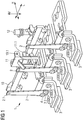
- FIG. 1 a perspective view of a first embodiment of a thermal trip device 1 arranged at a current conductive element 3 is shown.
- the current conductive element 3 extends in horizontally direction H at least partially.
- a bimetal element 2 contacts the current conductive element 3, wherein a second end 2.2 or lower end 2.2, respectively, of the bimetal element 2 is arranged and advantageously fixed at the current conductive element 3 with fixing elements 4, for example.
- Non-detachably or detachably arranged fixing elements 4 are for example screws, rivets or comparable elements.
- the first end 2.1 or upper end 2.1, respectively, of the bimetal element 2 is able to contact a tripping slide 10 tripping and especially a contacting area of the tripping slide 10, when a trip event is occurred.
- the bimetal element 2 is heated up by means of the current flowing through the current conductive element 3 and is moved or deflected especially by means of its first end 2.1 in direction to the tripping slide 10.
- the bimetal element 2 extend in a vertically direction V at least partially.
- the tripping slide 10 arranged at a kicker 11 or a kicker element 11, respectively, has a release element 10.1 in form of a protrusion extending from the tripping slide 10 in direction to the kicker 11.
- the release element 10.1 contacts a yoke element 11.1 of the kicker 11 in order to hold the kicker 11 in a first position or an initial position, respectively, in which the current path is not interrupt. Therefore, the release element 10.1 has a hook intervening at the yoke element 11.1.
- the position of the tripping slide 10 is adjustable in order to adjust a reaction time of the tripping slide 10 for releasing the kicker 11, for example.
- Fig. 2 shows a side view of a further embodiment of a thermal trip device 1 arranged at a current conductive element 3 and having a linking element 20.
- the arrangement of the bimetal element 2, the current conductive element 3, the tripping slide 10 and the kicker 11 essentially corresponds to the arrangement of these parts or elements, respectively, mentioned above with respect to fig. 1 . Therefore, the explanations mentioned above about these elements serves as basis for the following explanations.
- the linking element 20 extends from the current conductive element 3 to the bimetal element 2 in order to realize a current path to lead or redirect, respectively, the electrical current.
- the linking element 20 has one end 20.1 or an upper end 20.1, respectively, which contacts the bimetal element 2 between its first end 2.1 and its second end 2.2.
- the other end 20.2 or lower end 20.2, respectively, of the linking element 20 contacts the current conductive element 3. Therefore, the linking element 20 is an intermediate piece or connecting piece, respectively, between the bimetal element 2 and the current conductive element 3.
- the linking element 20 is a copper braid having at least partially a flexible material in order to allow a movement of the bimetal element 2 during a trip event is occurred in direction to the tripping slide 10 without damaging the linking element 20 arranged at the bimetal element 2.
- the material of the linking element 20 is electrically conductive at least partially.
- electrical current flowing through the current conductive element 3 is redirected from conductive element 3 via the bimetal element 2 and the linking element 20 back to the current conductive element 3. This new current path is shown with reference sign C.
- electrical current flowing through the bimetal element 2 results in increasing temperature of the bimetal element and in deflection and force of the latter, without affecting the temperature restrictions on lugs 30.
- the linking element 20 is welded with its one side to the centre of the bimetal element 2, wherein the centre of the bimetal element 2 extends between the first end 2.1 and the second end 2.1 of the bimetal element. Furthermore, it is conceivable that the other end 20.2 of the linking element 20 is welded to the current conductive element 3, which is a current conductive line or a load terminal, for example.
- At least one lug 30 is arranged at the current conductive element 3, which is formed like a current conductive line, for example.
- the first end 2.1 of the bimetal element 2 is arranged at a contacting element 5 contacting the tripping slide 10.
- the first end 2.1 of the bimetal element 2 moves in direction to the tripping slide 10. Therefore, the contacting element 5 pushes the tripping slide 10 in direction away from the bimetal element 2. Basing on this movement, the tripping slide 10 rotates about its longitudinal axis L1 (for example shown in fig.3 ) extending essentially in longitudinal direction L.
- the release element 10.1 of the tripping slide 10 releases the kicker 11 in such a way that the kicker 11 also rotates about its longitudinal axis L2 (for example shown in fig. 3 ) extending in longitudinal direction L in order to interrupt a current flow of electrical current.
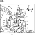
- a perspective view of an embodiment of a switching device 40 is shown.
- the switching device 40 is a part of the thermal magnetic circuit breaker having at least a thermal trip device and/or a magnetic trip device.
- the switching device 40 has at least a thermal trip device shown in fig. 1 or 2 , and therefore a bimetal element 2, a current conductive element 3, a tripping slide 10, a kicker 11 and/or a mechanism trip bar 16, especially shown in fig, 5 .
- the kicker 11 has a spring element 15 like a torsion spring, for example, in order to move the kicker 11 around its longitude axis L2, when the kicker 11 is released. Therefore, the kicker 11 rotates in clockwise direction.
- a knob 12 and a knob 13 are arranged at the switching device 40.
- an adjustment of the tripping slide 10 is possible, for example.
- an adjustment of the magnetic trip device is possible, for example.
- the magnetic tip device especially shown in fig. 6 , has inter alia a pin 14 extending in vertical direction V in order to lead an armature and especially an armature locator, also shown in fig. 6 .
- the kicker 11 has a protrusion 11.1 and especially a hitting protrusion 11.2, which is able to unlatch a mechanism trip bar 16 during a trip event is occurred and therefore during the tripping slide 10 rotates around its longitudinal axis L1 in order to release the kicker 11, which also rotates around its longitudinal axis L2.
- a perspective view of an embodiment of a magnetic trip device 50 arranged at a current conductive element 3 is shown.
- the current conductive element 3 contacts a yoke 60 and especially its upper layer 60.1 or first layer 60.1, respectively. Therefore, the current conductive element 3 extends through the yoke 60 and essentially between the legs of the yoke 60 along the yoke 60.
- the current conductive element 3 for conducting an electrical current along an electrical path has a recess (hidden in the present view), which is formed like a hole or a bore for example.
- a protrusion area 70.1 like a nose or a hook of an adjustment element 70 extends into this recess.
- the adjustment element 70 which is preferably designed like a calibration plate has a L-shape with respect to its cross-section, wherein one leg of the L is the protrusion area 70.1 and the other leg of the L is a contacting area 70.2 extending essentially at least partially parallel to a surface of the current conductive element 3 in the area of the yoke 60.
- the contacting area 70.2 is used to clamp a spring element 80 between the adjustment element 70 and an armature locator 90.
- the lower end of the spring element 80 contacting the adjustment element 70 is fixed with the adjustment element 70, wherein for example an end of the winding of the spring element 80 extends into the contacting area 70.2 and especially into a recess or such a thing of the contacting area 70.2 of the adjustment element 70.
- the spring element 80 is removable arranged at or fixed with the adjustment element 70.
- the spring element 80 extending between the adjustment element 70 and the armature locator 90 extends through the armature element 91 and especially through a bore 91.1 or a through-hole 91.1 of the armature element 91.
- the spring element 80 surrounds the pin 14 and especially the perimeter of the pin 14.
- the upper end or an upper area, respectively, of the spring element 80 is arranged inside a not shown recess or counterbore, respectively, of the armature locator 90.
- the spring element 80 has a defined spring load and spaces the armature 91 from the yoke 60, when no trip event like a short circuit is occurred.
- the pin 14 extends also through an adjustment bar 100, wherein the lower part of the pin 14 has a not shown threaded portion and especially an external thread, which is moveably engaged with a not shown internal thread of the adjustment element 70 and/or with a not shown internal thread of the current conductive element 3.
- the adjustment bar 100 has a not shown transfer element extending at least partially in a horizontal direction H away from the adjustment bar 100 in order to contact a tripping slide 10 shown in fig. 1 , for example.
- the armature locator 90 and the adjustment bar 100 arranged to the armature locator 90 are moved in vertical direction V along the pin 14. Therefore, the transfer element is also moved in direction to the yoke 60 and especially in vertical direction V. Basing on this movement, the tripping slide 10 is pushed to its final position, where the energy storage (not shown in fig. 6 ) is released.
- the armature locator 90 When the adjustment bar 100 is moved in a horizontal direction H, for example in direction to the armature locator 90 (leftwards), the armature locator 90 is moved downwards in direction to the yoke 60 and therefore in vertical direction V. Basing on this movement, the distance between the armature element 91 and the yoke 60 is reduced.
- the transformation of the horizontal movement of the adjustment bar 100 into a vertical movement of the armature locator 90 is done by means of both, the inclined area 110.1 or inclined surface 110.1, respectively, of the protrusion 110 of the adjustment bar 100 and the inclined area 90.1 or surface 90.1, respectively, of the armature locator 90.
- Both, inclined area 110.1 and inclined area 90.1 contact each other and are movable arranged to each other in such a way that the inclined areas 110.1 and 90.1 slide against each other. Therefore, during a horizontal movement of the adjustment bar 100 in direction away from the armature locator 90 (rightwards), the armature locator 90 is moved in vertical direction V away from the yoke 60 (upwards) due to the spring load of the spring element 80. That means that the spring element 80 pushes back the armature locator 90.
- the adjustment bar 100 is only shown in sections in fig. 6 and has preferably more than one protrusion 110 and especially two or three protrusions 110 in order to contact two or three single magnetic trip devices 50, for example as a three pole arrangement.
Description
- The present invention is directed to a thermal trip device of a thermal magnetic circuit breaker, wherein the thermal trip device has at least a bimetal element adapted to interrupting a current flow. The preset invention is also directed to a switching device having at least a bimetal element, a current conductive element, a tripping slide, a linking element and/or a kicker element. Furthermore, on the one hand, the present invention is directed to a thermal magnetic circuit breaker having a thermal trip device like mentioned above and on the other hand to a method for protecting an electric circuit from damage by overload by means of a thermal trip device of a thermal magnet circuit breaker.
- Essentially, it is known that a thermal magnetic circuit breaker is a manually or automatically operating electrical switch designed to protect an electrical circuit from damage caused by overload or short circuit, for example. Its basic function is the detection of a fault condition and the interruption of current flow. Therefore, the thermal magnetic circuit breaker has for example at least one magnetic trip device in order to prevent the electrical circuit or an electrical device from damage by short circuit and a thermal trip device in order to prevent the electric circuit or an electrical device, like a load, from damage by overload. A short circuit is an abnormal connection between two nodes of the electric circuit intended to be at different voltages. This results in an excessive electric current, named an overcurrent limited only by the Thévenin equivalent resistance of the rest of the network and potentially causes circuit damage, overheating, fire or explosion. An overload is a less extreme condition but a longer-term over-current condition as a short circuit.
- The thermal magnetic circuit breaker or breaker, respectively, has different settings or adjustments, respectively, as to where does the client wants the breaker to trip thermally. These settings go from 0.7 ln to 1 ln, wherein 0.7 ln means 70% of the nominal current rated on the breaker and 1 ln means 100% of the nominal current rated on the breaker. Therefore, in a 140 Amp breaker, 70% will be 700 Amp. Basing on a lower thermal adjustment, less electrical current goes through a conductive element like a conductor and results on a lower temperature on a bimetal element of the thermal trip device. Thus, the temperature profile of the thermal trip device of the thermal magnetic circuit breaker or thermal magnetic trip unit (TMTU) presents low temperature behaviour on the lower thermal adjustment side, which is for example 70% ln and therefore 70% of the nominal current, as mentioned above. Since the movement of the bimetal element is a result of the temperature, such a low temperature is not enough in order to reach deflection and force of the bimetal element of the thermal trip device, which are necessary to unlatch the breaker mechanism. Therefore, a lower electrical current inducts a less temperature and as a consequence a less deflection and/or force of the bimetal element, during a high electrical current inducts a higher temperature and as a consequence a higher deflection and/or force of the bimetal element.
-
US 4 163 881 A discloses a circuit breaker having an improved compact thrust transmitting spring for opening the contacts in a minimum of time. The circuit breaker having a stationary contact, a movable contact, a contact arm carrying said movable contact, a trip structure, a toggle comprising a first link pivotally connected to said contact arm and a second link pivotally connected to said trip structure, a knee pivot pivotally connecting said first and second links, a manually operable operating member, a thrust-transmitting link between the said operating member and said knee pivot, said operating member being manually movable to a closed position to operate through said thrust-transmitting link to cause said toggle to thrust said contact arm to the closed position, the improvement wherein the contact arm is pivotally mounted on a pinhole axis, bias means for biasing the contact arm to the open position to effect increased separation of the contacts and comprising a wire spring pivoted on the pinhole axis and having first and second end portions, the movable contact being mounted on one side surface of the contact arm, the first end portion of the wire spring bearing against the opposite side surface of the arm, and the second end portion of the spring being fixedly mounted. - In
DE 34 10 340 A1 a meter preliminary automatic circuit breaker is disclosed, as a replacement for the house-connection fuse, is composed of a melting fuse cartridge, which is held in a plug-in or screw socket element (which can be lead sealed) and of a protection circuit breaker which can be manually operated and has thermal overcurrent tripping and trip-free operation, which are arranged inside a common housing and are connected electrically in series between the connecting terminals which are placed on the outside. In order to counteract a wide range of types and the re-equipment necessity associated therewith, and at the same time to make the specified melting fuse virtually proof against failure for the region inside the installation, on the one hand a changeover device (which can be lead sealed) is provided on the preliminary automatic circuit breaker, by means of which the response value of the thermal trip device in the form of a bimetallic strip can be changed from the outside mechanically and/or electrically for optionally increasing the current extraction capability by the insertion of a special insertion part, and on the other hand the melting fuse is dimensioned to have its rated current value in each case above that of the thermal trip device. - Thus, it is the object of the present invention to overcome the disadvantages mentioned above and to provide a thermal magnetic circuit breaker and especially a thermal trip device of a thermal magnetic circuit breaker and more especially a switching device, which allow in an easy and cost-effective manner a triggering of the thermal magnetic circuit breaker and especially an element of the thermal magnetic circuit breaker in order to interrupt a current flow of the electrical circuit in order to protect the circuit and the loads of latter from damage.
- The object of the present invention is solved by a thermal trip device according to the features of claim 1, by a switching device according to the features of claim 6, by a thermal magnetic circuit breaker according to the features of claim 7 and a method for protection an electric circuit from damage by overload by means of a thermal trip device of a thermal magnet circuit breaker according to the features of claim 9. Further features and details of the invention are subject of the sub claims and/or emerge from the description and the figures. Features and details discussed with respect to the thermal trip device can also be applied to the switching device, the thermal magnetic circuit breaker and/or the method for protecting an electric circuit from damage and vice versa.
- The thermal trip device of a thermal magnet circuit breaker for protecting an electrical circuit from damage by overload has at least a bimetal element in order to be arranged with its second end at a current conductive element for conducting electrical current and in order to be arranged with its first end at a tripping slide adapted to interrupting a current flow, wherein the bimetal element is able to be connected with a linking element extending between the bimetal element and the current conductive element in order to redirect the electrical current at least partially.
- Advantageously, the thermal trip device is a part of the thermal magnetic circuit breaker mentioned above and has at least a bimetal element, which is composed of at least two separate metals joined together. The bimetal element consist of two layers of different metals, for example, wherein bimetal elements having three or four separate metals or layers, respectively, are referred to as trimetal or tetrametal. Therefore, the bimetal element of the present inventions is also able to have three, four or more than four separate metals or layer, respectively.
- The electrical current flowing through the conductive element emits heat, by which the bimetal element or trimetal element or tetrametal element, and so on, is heated, wherein due to this heat, a movement and especially a deflection of the bimetal element is triggered. That means, basing on the nature of the bimetal element, it converts the heat or temperature, respectively, into mechanical displacement generating certain amount of force. Thus, the amount of heat restricts the amount of force that will generate. Increasing the temperature generally of the current path and especially in the area of the conductive element of the thermal trip device results for example in overheating of lugs arranged at least nearly the conductive element above especial requirement specifications and therefore above for example 50°C. Thus, an increasing of the temperature in order to optimize the movement of the bimetal element in order to interrupt the electrical current flow of the current circuit for protecting the circuit from overload and so on, leads to damage loads or comparable products. In the context of the present invention the electrical circuits includes also at least one load like an electrical device.
- The bimetal element has a second end, also named lower end and a first end, also named upper end, wherein the second end contacts at least partially a part of the current conductive element conducting electrical current along at least a part of the current path. Heat or thermal radiation, respectively, emitted by the electrical current flowing through the current conductive element moves from the current conductive element above the second end of the bimetal element to the bimetal element in such a way that the bimetal element is heated indirectly. The heat causes the bimetal element to deflect, wherein the bimetal element applies a force into a tripping slide. That means that the area of the first end of the bimetal element moves in direction to the tripping slide in order to contact at least a contact zone of the tripping slide. If the movement or deflection, respectively, is not stopped the first end of the bimetal element press against the tripping slide. Basing on the movement of the bimetal element, the tripping slide rotates clockwise around a longitudinal axis and releases a kicker for interrupting the current flow.
- According to the present invention, the thermal trip device and especially the bimetal element of the thermal trip device is able to contact and is advantageously arranged at a linking element. It is also conceivable that the linking element is a part of the thermal trip device. By means of the linking element, it is possible to heat the bimetal element directly and indirectly. Therefore, electrical current is redirected at least partly along the linking element and especially at least along a part of the bimetal element connected with the conductive element and the linking element, advantageously.
- Advantageously, the linking element is arranged with its one end between the first end and the second end of the bimetal element and in particular in a middle area of the bimetal element with respect to its longitudinal axis. Therefore, electrical current or current, respectively, flows from the current conductive element shaped as current line, for example, via at least a part of the bimetal element and especially a lower part of the bimetal element back to the current conductive element. It is also conceivable that the one end of the linking element is arranged at the upper end or essentially near the upper end of the bimetal element or at the lower end or essentially near the lower end of the bimetal element and therefore in an upper or lower area of the bimetal element.
- Advantageously, the linking element has a flexible material having at least partially a linear elastic behaviour. For example, the Hooke's law describes the elastic behaviour of components where deformation is proportional to the load acting upon them. By means of the flexible or elastic material, respectively, a movement of the bimetal element is possible without damage the linking element arranged at and especially fixed with the bimetal element at least partially.
- Therefore, it is conceivable that the linking element has a well-conductive material like a copper material and is especially a copper braid. Copper is a ductile metal with very high thermal and electrical conductivity, wherein especially pure copper is soft and malleable. Therefore, copper is useable as a conductor of heat and electricity. It is also conceivable that other elastic and thermal conductive and electrical conductive materials are used individually or in combination.
- With respect to the present invention, it is conceivable that the linking element is adjustable arranged at the bimetal element and/or at the current conductive element. Advantageously, basing on this adjustment, the length of the current path leading the electrical current along the bimetal element is variable. Thus, also the temperature or heat heating the bimetal element is variable. The adjustable arrangement is realisable for example by means of fixing elements like clamps or such comparable elements. It is also conceivable that the one end and/or the second end of the fixing element are welded on the bimetal element and/or the current conductive element.
- Advantageously, the linking element has at least a length of circa 3 cm and/or a diameter of circa 4 mm.
- By means of the linking element, a technical contradiction is solved, wherein temperature on the bimetal element is increased without going over permissible temperature on the lugs due to selective heating, for example. Therefore, a direct and indirect heating of the bimetal element that allows thermal adjustment on the low side is combined, advantageously.
- Furthermore, a switching device having at least a bimetal element in order to be arranged with its second end at a current conductive element and in order to be arranged with its first end at a tripping slide is claimed. It is advantageously conceivable that the switching element also has the current conductive element for conducting electrical current, the tripping slide adapted to interact with a kicker element, a linking element extending between the bimetal element and the current conductive element in order to redirect the electrical current at least partially and/or the kicker element in order to hitch a mechanism trip bar unlatching a breaker mechanism to interrupt the current flow. Advantageously, the switching device combines different devices and/or elements like the thermal trip device or the bimetal element of the thermal trip device with a kicker, for example, in order to generate an activity chain by means of different devices and/or elements working together in order to interrupt a current flow during a trip event like an overload and so on I occurred. Current flowing through the conductive element flows via at least a part of the bimetal element and via the linking element back to the current conductive element arranged at the bimetal element and also at the linking element and formed like a current line, for example. When the bimetal element starts heating up by means of the current flowing though the latter, especially the upper end of the bimetal element moves or deflects, respectively, towards the tripping slide and pushes latter in such a way that the tripping slide rotates around its axis in clockwise direction. Due to the rotation of the tripping slide, the kicker, which is loaded with a spring element like a torsion spring, for example, is released. Therefore, the kicker held in position due to a latch feature of the tripping slide, the kicker moves forward with the help of the spring element in direction to a mechanism trip bar. The mechanism trip bar unlatches the thermal magnet circuit breaker mechanism and opens contact blades in order to interrupt current flow.
- The switching device mentioned above also has all advantages mentioned above concerning the thermal trip device.
- Furthermore, a thermal magnetic circuit breaker for protecting an electrical circuit from damage caused by overload or short circuit is claimed, wherein the thermal magnetic circuit breaker has at least a thermal trip device according to one of the preceding claims and therefore a thermal trip device like mentioned above.
- Advantageously, the thermal magnetic circuit breaker, also named thermal magnetic trip unit (TMTU), has a translational magnetic system and especially a translational magnetic trip device with a common adjustment system like an adjustment bar for an instantaneous setting.
- It is conceivable that the magnetic trip device of the thermal magnetic circuit breaker has an armature element reacting to a magnetic field resulting from current flowing through a solenoid element. Advantageously, the magnetic trip device has at least an armature element movable arranged with respect to a yoke or especially to a current conductive element conducting electrical energy or current, respectively. The armature element or armature, respectively, is a magnetic element and especially a pole piece having at least partially an iron material and reacting to a magnetic field created by the yoke during a trip moment. In order to realize a guided movement of the armature element towards the yoke at least during a trip event like a short circuit, the armature element is arranged on an armature locator. The armature locator is moveable arranged on a pin extending from an adjustment bar towards the yoke, for example. The armature locator or the adjustment bar can be connected with a tripping slide, which is able to interrupt a current flow of the current circuit, when the tripping slide is moved due to a movement of the armature locator or the adjustment bar in conjunction with the armature element towards the yoke because of a magnetic force.
- The thermal magnetic circuit breaker mentioned above also has all advantages mentioned above concerning the thermal trip device and/or the switching device.
- Furthermore, a method for protecting an electric circuit from damage by overload by means of a thermal trip device of a thermal magnet circuit breaker is claimed. According to this method, an electric current is conducted at least partially from a current conductive element via at least a part of a bimetal element arranged with its lower end on the current conductive element, along a linking element arranged essentially between the current conductive element and the bimetal element, back to the current conductive element in order to heat or temperature the bimetal element to obtain a mechanical displacement of at least one area of the bimetal element.
- Like mentioned above a first or upper end, respectively, of the bimetal element contacts a part of a tripping slide at least indirectly, when the bimetal element heats up und a mechanical displacement of at least the first end of the bimetal element is obtained. Afterwards, the tripping slide pushed by the upper end of the bimetal element releases a kicker. Due to a movement of the released kicker, a mechanism trip bar is hit in order to unlatch a breaker mechanism to interrupting a current flow.
- Advantageously, the thermal trip device is made according to one of the preceding claims and therefore like mentioned above.
- Advantageously, by means of the present invention a combination of directly and indirectly heated bimetal element basic concept is used, wherein especially a heat spot or selective heating method was created to be applied on a specific area.
- The method mentioned above also has all advantages mentioned above concerning the thermal trip device and/or the switching device and/or the thermal magnetic circuit breaker.
- Embodiments of a thermal trip device and of a magnetic trip device of a thermal magnetic circuit breaker and a switching device are explained in more detail with reference to the accompanying drawings. The drawings show schematically in:
- Figure 1:
- a perspective view of a first embodiment of a thermal trip device arranged at a current conductive element for example,
- Figure 2:
- a side view of an embodiment of a thermal trip device arranged at a current conductive element and having a linking element,
- Figure 3:
- a perspective view of an embodiment of a switching device,
- Figure 4:
- a side view of different parts of a switching device,
- Figure 5:
- a perspective view of the switching device shown in
fig. 3 , and - Figure 6:
- a perspective view of an embodiment of a magnetic trip device of a thermal magnetic circuit breaker arranged on a current conductive element.
- Elements having the same function and mode of action are provided in
figures 1 to 6 with the same reference signs. - In
fig. 1 a perspective view of a first embodiment of a thermal trip device 1 arranged at a currentconductive element 3 is shown. The currentconductive element 3 extends in horizontally direction H at least partially. Abimetal element 2 contacts the currentconductive element 3, wherein a second end 2.2 or lower end 2.2, respectively, of thebimetal element 2 is arranged and advantageously fixed at the currentconductive element 3 with fixingelements 4, for example. Non-detachably or detachably arranged fixingelements 4 are for example screws, rivets or comparable elements. The first end 2.1 or upper end 2.1, respectively, of thebimetal element 2 is able to contact a trippingslide 10 tripping and especially a contacting area of the trippingslide 10, when a trip event is occurred. That means, if an overload is occurred thebimetal element 2 is heated up by means of the current flowing through the currentconductive element 3 and is moved or deflected especially by means of its first end 2.1 in direction to the trippingslide 10. Thebimetal element 2 extend in a vertically direction V at least partially. - The tripping
slide 10 arranged at akicker 11 or akicker element 11, respectively, has a release element 10.1 in form of a protrusion extending from the trippingslide 10 in direction to thekicker 11. The release element 10.1 contacts a yoke element 11.1 of thekicker 11 in order to hold thekicker 11 in a first position or an initial position, respectively, in which the current path is not interrupt. Therefore, the release element 10.1 has a hook intervening at the yoke element 11.1. - With a
knob 12, the position of the trippingslide 10 is adjustable in order to adjust a reaction time of the trippingslide 10 for releasing thekicker 11, for example. -
Fig. 2 shows a side view of a further embodiment of a thermal trip device 1 arranged at a currentconductive element 3 and having a linkingelement 20. The arrangement of thebimetal element 2, the currentconductive element 3, the trippingslide 10 and thekicker 11 essentially corresponds to the arrangement of these parts or elements, respectively, mentioned above with respect tofig. 1 . Therefore, the explanations mentioned above about these elements serves as basis for the following explanations. - The linking
element 20 extends from the currentconductive element 3 to thebimetal element 2 in order to realize a current path to lead or redirect, respectively, the electrical current. The linkingelement 20 has one end 20.1 or an upper end 20.1, respectively, which contacts thebimetal element 2 between its first end 2.1 and its second end 2.2. The other end 20.2 or lower end 20.2, respectively, of the linkingelement 20 contacts the currentconductive element 3. Therefore, the linkingelement 20 is an intermediate piece or connecting piece, respectively, between thebimetal element 2 and the currentconductive element 3. Advantageously, the linkingelement 20 is a copper braid having at least partially a flexible material in order to allow a movement of thebimetal element 2 during a trip event is occurred in direction to the trippingslide 10 without damaging the linkingelement 20 arranged at thebimetal element 2. The material of the linkingelement 20 is electrically conductive at least partially. Thus, electrical current flowing through the currentconductive element 3 is redirected fromconductive element 3 via thebimetal element 2 and the linkingelement 20 back to the currentconductive element 3. This new current path is shown with reference sign C. Advantageously, electrical current flowing through thebimetal element 2 results in increasing temperature of the bimetal element and in deflection and force of the latter, without affecting the temperature restrictions onlugs 30. It is conceivable that the linkingelement 20 is welded with its one side to the centre of thebimetal element 2, wherein the centre of thebimetal element 2 extends between the first end 2.1 and the second end 2.1 of the bimetal element. Furthermore, it is conceivable that the other end 20.2 of the linkingelement 20 is welded to the currentconductive element 3, which is a current conductive line or a load terminal, for example. - Near the
bimetal element 2 at least onelug 30 is arranged at the currentconductive element 3, which is formed like a current conductive line, for example. - The first end 2.1 of the
bimetal element 2 is arranged at a contacting element 5 contacting the trippingslide 10. Thus, when thebimetal element 2 is deflected basing on the heat of the electrical current flowing along the new electrical current path C, the first end 2.1 of thebimetal element 2 moves in direction to the trippingslide 10. Therefore, the contacting element 5 pushes the trippingslide 10 in direction away from thebimetal element 2. Basing on this movement, the trippingslide 10 rotates about its longitudinal axis L1 (for example shown infig.3 ) extending essentially in longitudinal direction L. Basing on this rotation, the release element 10.1 of the trippingslide 10 releases thekicker 11 in such a way that thekicker 11 also rotates about its longitudinal axis L2 (for example shown infig. 3 ) extending in longitudinal direction L in order to interrupt a current flow of electrical current. - In
fig. 3 , a perspective view of an embodiment of aswitching device 40 is shown. Advantageously, the switchingdevice 40 is a part of the thermal magnetic circuit breaker having at least a thermal trip device and/or a magnetic trip device. Advantageously, the switchingdevice 40 has at least a thermal trip device shown infig. 1 or2 , and therefore abimetal element 2, a currentconductive element 3, a trippingslide 10, akicker 11 and/or amechanism trip bar 16, especially shown infig, 5 . - Like shown in
fig. 3 and4 , whereinfig. 4 shows a side view of different parts of a switching device, thekicker 11 has aspring element 15 like a torsion spring, for example, in order to move thekicker 11 around its longitude axis L2, when thekicker 11 is released. Therefore, thekicker 11 rotates in clockwise direction. Furthermore, aknob 12 and aknob 13 are arranged at theswitching device 40. By means ofknob 12, an adjustment of the trippingslide 10 is possible, for example. Therefore, by means ofknob 13 an adjustment of the magnetic trip device is possible, for example. The magnetic tip device, especially shown infig. 6 , has inter alia apin 14 extending in vertical direction V in order to lead an armature and especially an armature locator, also shown infig. 6 . - Like shown in
fig. 5 , in which a perspective view of the switching device shown infig. 3 is pictured, for example, thekicker 11 has a protrusion 11.1 and especially a hitting protrusion 11.2, which is able to unlatch amechanism trip bar 16 during a trip event is occurred and therefore during the trippingslide 10 rotates around its longitudinal axis L1 in order to release thekicker 11, which also rotates around its longitudinal axis L2. - In
fig. 6 a perspective view of an embodiment of amagnetic trip device 50 arranged at a currentconductive element 3 is shown. The currentconductive element 3 contacts ayoke 60 and especially its upper layer 60.1 or first layer 60.1, respectively. Therefore, the currentconductive element 3 extends through theyoke 60 and essentially between the legs of theyoke 60 along theyoke 60. The currentconductive element 3 for conducting an electrical current along an electrical path has a recess (hidden in the present view), which is formed like a hole or a bore for example. A protrusion area 70.1 like a nose or a hook of anadjustment element 70 extends into this recess. Theadjustment element 70, which is preferably designed like a calibration plate has a L-shape with respect to its cross-section, wherein one leg of the L is the protrusion area 70.1 and the other leg of the L is a contacting area 70.2 extending essentially at least partially parallel to a surface of the currentconductive element 3 in the area of theyoke 60. The contacting area 70.2 is used to clamp aspring element 80 between theadjustment element 70 and anarmature locator 90. It is conceivable that the lower end of thespring element 80 contacting theadjustment element 70 is fixed with theadjustment element 70, wherein for example an end of the winding of thespring element 80 extends into the contacting area 70.2 and especially into a recess or such a thing of the contacting area 70.2 of theadjustment element 70. Advantageously, thespring element 80 is removable arranged at or fixed with theadjustment element 70. Thespring element 80 extending between theadjustment element 70 and thearmature locator 90 extends through thearmature element 91 and especially through a bore 91.1 or a through-hole 91.1 of thearmature element 91. Thespring element 80 surrounds thepin 14 and especially the perimeter of thepin 14. Advantageously, the upper end or an upper area, respectively, of thespring element 80 is arranged inside a not shown recess or counterbore, respectively, of thearmature locator 90. Thespring element 80 has a defined spring load and spaces thearmature 91 from theyoke 60, when no trip event like a short circuit is occurred. - The
pin 14 extends also through anadjustment bar 100, wherein the lower part of thepin 14 has a not shown threaded portion and especially an external thread, which is moveably engaged with a not shown internal thread of theadjustment element 70 and/or with a not shown internal thread of the currentconductive element 3. - It is conceivable that the
adjustment bar 100 has a not shown transfer element extending at least partially in a horizontal direction H away from theadjustment bar 100 in order to contact a trippingslide 10 shown infig. 1 , for example. Basing on the movement of thearmature element 91 in direction to theyoke 60 during a trip event, thearmature locator 90 and theadjustment bar 100 arranged to thearmature locator 90 are moved in vertical direction V along thepin 14. Therefore, the transfer element is also moved in direction to theyoke 60 and especially in vertical direction V. Basing on this movement, the trippingslide 10 is pushed to its final position, where the energy storage (not shown infig. 6 ) is released. - When the
adjustment bar 100 is moved in a horizontal direction H, for example in direction to the armature locator 90 (leftwards), thearmature locator 90 is moved downwards in direction to theyoke 60 and therefore in vertical direction V. Basing on this movement, the distance between thearmature element 91 and theyoke 60 is reduced. The transformation of the horizontal movement of theadjustment bar 100 into a vertical movement of thearmature locator 90 is done by means of both, the inclined area 110.1 or inclined surface 110.1, respectively, of theprotrusion 110 of theadjustment bar 100 and the inclined area 90.1 or surface 90.1, respectively, of thearmature locator 90. Both, inclined area 110.1 and inclined area 90.1 contact each other and are movable arranged to each other in such a way that the inclined areas 110.1 and 90.1 slide against each other. Therefore, during a horizontal movement of theadjustment bar 100 in direction away from the armature locator 90 (rightwards), thearmature locator 90 is moved in vertical direction V away from the yoke 60 (upwards) due to the spring load of thespring element 80. That means that thespring element 80 pushes back thearmature locator 90. Theadjustment bar 100 is only shown in sections infig. 6 and has preferably more than oneprotrusion 110 and especially two or threeprotrusions 110 in order to contact two or three singlemagnetic trip devices 50, for example as a three pole arrangement. -
- 1
- thermal trip device
- 2
- bimetal element
- 2.1
- first end/upper end of the bimetal element
- 2.2
- second end/lower end of the bimetal element
- 3
- current conductive element
- 4
- fixing element
- 5
- contacting element
- 10
- tripping slide
- 10.1
- release element
- 11
- kicker
- 11.1
- yoke element
- 11.2
- hitting protrusion
- 12
- knob
- 13
- knob
- 14
- pin
- 15
- spring element
- 16
- mechanism trip bar
- 20
- linking element
- 20.1
- one end/upper end of the linking element
- 20.2
- other end/lower end of the linking element
- 30
- lug
- 40
- switching device
- 50
- magnetic trip device
- 60
- yoke
- 60.1
- first layer of the yoke
- 60.2
- second layer of the yoke
- 70
- adjustment element
- 70.1
- protrusion area
- 70.2
- contacting area
- 80
- spring element
- 90
- armature locator
- 90.1
- inclined area of the armature locator
- 91
- armature element
- 91.1
- bore/hole
- 100
- adjustment bar
- 110
- protrusion
- C
- new/alternative electrical current path
- H
- horizontal direction
- L
- longitudinal direction
- L1
- longitudinal axis if the tripping slide
- L2
- longitudinal axis of the kicker
- V
- vertical direction
Claims (9)
- Thermal trip device (1) of a thermal magnet circuit breaker for protecting an electrical circuit from damage by overload, wherein the thermal trip device (1) has at least a bimetal element (2) in order to be arranged with its second end (2.2) at a current conductive element (3) for conducting electrical current and in order to be arranged with its first end (2.1) at a tripping slide (10) adapted to interrupting a current flow, wherein the bimetal element (2) is able to be connected with a linking element (20) extending between the bimetal element (2) and the current conductive element (3) in order to redirect the electrical current at least partially, characterized in that,
the linking element (20) is adjustable arranged at the bimetal element (2) and/or at the current conductive element (3). - Thermal trip device (1) according to claim 1, characterized in that,
the linking element (20) is arranged with its one end (20.1) between the first end (2.1) and the second end (2.2) of the bimetal element (2) and in particular in a middle area of the bimetal element (2) with respect to its longitudinal axis. - Thermal trip device (1) according to one of the preceding claims 1 or 2,
characterized in that,
the linking element (20) has a flexible material having at least partially a linear elastic behavior. - Thermal trip device (1) according to one of the preceding claims,
characterized in that,
the linking element (20) has a well-conductive material like a copper material and is especially a copper braid. - Switching device (40) having at least a thermal trip device (1) according to one of the preceding claims, the bimetal element (2) in order to be arranged with its first end (2.1) at a tripping slide (10), the first end (2.1) adapted to interact with a kicker (11) element and/or the tripping slide (10) in order to hitch a mechanism trip bar (16) unlatching a breaker mechanism to interrupt the current flow.
- Thermal magnetic circuit breaker for protecting an electrical circuit from damage caused by overload or short circuit, having at least a thermal trip device (1) according to one of the preceding claims 1 to 4.
- Thermal magnetic circuit breaker according to claim 6, characterized in that,
the thermal magnetic circuit breaker has a magnetic trip device (50), which has at least an armature element (91) reacting to a magnetic field resulting from current flowing through a solenoid element - Method for protecting an electric circuit from damage by overload by means of a thermal trip device (1) of a thermal magnet circuit breaker, wherein an electric current is conducted at least partially from a current conductive element (3) via at least a part of a bimetal element (2) arranged with its lower end (2.2) on the current conductive element (3), along a linking element (20) arranged between the current conductive element (3) and the bimetal element (2), the linking element (20) is adjustable arranged at the bimetal element (2) and/or at the current conductive element (3), back to the current conductive element (3) in order to heat the bimetal element (2) to obtain a mechanical displacement of at least one area of the bimetal element (2) at a tripping slide (10) adapted to interrupting a current flow.
- Method according to claim 9,
characterized in that,
the thermal trip device (1) is made according to one of the preceding claims 1 to 5.
Priority Applications (2)
| Application Number | Priority Date | Filing Date | Title |
|---|---|---|---|
| EP14151594.0A EP2897152B1 (en) | 2014-01-17 | 2014-01-17 | Thermal trip device, switching device, thermal magnetic circuit breaker and method for protecting an electric circuit |
| US14/522,706 US9508516B2 (en) | 2014-01-17 | 2014-10-24 | Thermal trip device having a current redirecting linking element, switching device, thermal magnetic circuit breaker and method for protecting an electric circuit |
Applications Claiming Priority (1)
| Application Number | Priority Date | Filing Date | Title |
|---|---|---|---|
| EP14151594.0A EP2897152B1 (en) | 2014-01-17 | 2014-01-17 | Thermal trip device, switching device, thermal magnetic circuit breaker and method for protecting an electric circuit |
Publications (2)
| Publication Number | Publication Date |
|---|---|
| EP2897152A1 EP2897152A1 (en) | 2015-07-22 |
| EP2897152B1 true EP2897152B1 (en) | 2017-03-29 |
Family
ID=49943274
Family Applications (1)
| Application Number | Title | Priority Date | Filing Date |
|---|---|---|---|
| EP14151594.0A Not-in-force EP2897152B1 (en) | 2014-01-17 | 2014-01-17 | Thermal trip device, switching device, thermal magnetic circuit breaker and method for protecting an electric circuit |
Country Status (2)
| Country | Link |
|---|---|
| US (1) | US9508516B2 (en) |
| EP (1) | EP2897152B1 (en) |
Families Citing this family (3)
| Publication number | Priority date | Publication date | Assignee | Title |
|---|---|---|---|---|
| EP2911178B1 (en) * | 2014-02-25 | 2017-09-13 | Siemens Aktiengesellschaft | Magnetic trip device of a thermal magnetic circuit breaker having an adjustment element |
| EP2911177B1 (en) * | 2014-02-25 | 2017-09-13 | Siemens Aktiengesellschaft | Magnetic trip device of a thermal magnetic circuit breaker having a stabilizer element |
| DE102016208930A1 (en) * | 2016-05-24 | 2017-11-30 | Siemens Aktiengesellschaft | Overload release |
Family Cites Families (6)
| Publication number | Priority date | Publication date | Assignee | Title |
|---|---|---|---|---|
| US4163881A (en) * | 1977-09-29 | 1979-08-07 | Westinghouse Electric Corp. | Circuit breaker with thrust transmitting spring |
| DE3410340A1 (en) * | 1984-03-21 | 1985-10-03 | Heinrich Kopp Gmbh & Co Kg, 8756 Kahl | Meter preliminary automatic circuit breaker |
| DE9401785U1 (en) * | 1994-02-03 | 1995-07-20 | Kloeckner Moeller Gmbh | Key switch with a locking mechanism |
| FR2722331B1 (en) * | 1994-07-08 | 1996-09-27 | Legrand Sa | THERMAL SUB-ASSEMBLY FOR CIRCUIT BREAKER |
| US6181226B1 (en) * | 1999-11-05 | 2001-01-30 | Siemens Energy & Automation, Inc. | Bi-metal trip unit for a molded case circuit breaker |
| WO2013126061A1 (en) * | 2012-02-23 | 2013-08-29 | Siemens Aktiengesellschaft | Circuit breaker heaters and translational magnetic systems |
-
2014
- 2014-01-17 EP EP14151594.0A patent/EP2897152B1/en not_active Not-in-force
- 2014-10-24 US US14/522,706 patent/US9508516B2/en not_active Expired - Fee Related
Non-Patent Citations (1)
| Title |
|---|
| None * |
Also Published As
| Publication number | Publication date |
|---|---|
| EP2897152A1 (en) | 2015-07-22 |
| US9508516B2 (en) | 2016-11-29 |
| US20150206688A1 (en) | 2015-07-23 |
Similar Documents
| Publication | Publication Date | Title |
|---|---|---|
| US8830026B2 (en) | Shape memory alloy actuated circuit breaker | |
| KR101096988B1 (en) | Trip device | |
| JP6357221B2 (en) | Protective device | |
| CA2715429A1 (en) | Switching device | |
| US6529112B1 (en) | Ring tongue lug retainer molded case circuit breaker | |
| EP2897152B1 (en) | Thermal trip device, switching device, thermal magnetic circuit breaker and method for protecting an electric circuit | |
| US20080186643A1 (en) | Voltage surge protection device with a movable contact comprising selective disconnection means against short-circuits | |
| US6181226B1 (en) | Bi-metal trip unit for a molded case circuit breaker | |
| EP2905800A1 (en) | Thermal trip device, switching device, thermal magnetic circuit breaker and method for protecting an electrical circuit from damage | |
| EP0081290B1 (en) | Fail safe circuit breaker | |
| US9130354B2 (en) | Rapid disconnect device | |
| EP2913836A1 (en) | Thermal trip device of a thermal magnetic circuit breaker having a resistor element, thermal magnetic circuit breaker and switching device for interrupting a current flow and method for protecting an electrical circuit from damage | |
| JP4905112B2 (en) | Circuit breaker overcurrent trip device | |
| AU2009221605A1 (en) | Switching device | |
| MX2014010125A (en) | Circuit breaker heaters and translational magnetic systems. | |
| US3313898A (en) | Circuit breaker with thermal trip device of high short-circuit withstandability | |
| KR100479434B1 (en) | Trip device of circuit braker | |
| US3032631A (en) | Circuit breaker having electrical and mechanical coordination with a current limiting device | |
| CN109950104B (en) | Thermomagnetic trip assembly and electrical switch unit | |
| US10079132B1 (en) | Systems, apparatus, and methods for electric circuit breaker tripping | |
| KR100434332B1 (en) | isolation device of electric current in circuit breaker | |
| US3260825A (en) | Circuit breaker with ambient compensating means | |
| KR102003329B1 (en) | Circuit breaker having improved structure for preventing internal short | |
| KR20040003596A (en) | trip portion structure of MCCB | |
| KR200471898Y1 (en) | Circuit breaker |
Legal Events
| Date | Code | Title | Description |
|---|---|---|---|
| PUAI | Public reference made under article 153(3) epc to a published international application that has entered the european phase |
Free format text: ORIGINAL CODE: 0009012 |
|
| 17P | Request for examination filed |
Effective date: 20140117 |
|
| AK | Designated contracting states |
Kind code of ref document: A1 Designated state(s): AL AT BE BG CH CY CZ DE DK EE ES FI FR GB GR HR HU IE IS IT LI LT LU LV MC MK MT NL NO PL PT RO RS SE SI SK SM TR |
|
| AX | Request for extension of the european patent |
Extension state: BA ME |
|
| 17P | Request for examination filed |
Effective date: 20160107 |
|
| RBV | Designated contracting states (corrected) |
Designated state(s): AL AT BE BG CH CY CZ DE DK EE ES FI FR GB GR HR HU IE IS IT LI LT LU LV MC MK MT NL NO PL PT RO RS SE SI SK SM TR |
|
| GRAP | Despatch of communication of intention to grant a patent |
Free format text: ORIGINAL CODE: EPIDOSNIGR1 |
|
| RIC1 | Information provided on ipc code assigned before grant |
Ipc: H01H 71/08 20060101ALI20160930BHEP Ipc: H01H 71/16 20060101AFI20160930BHEP |
|
| INTG | Intention to grant announced |
Effective date: 20161104 |
|
| GRAS | Grant fee paid |
Free format text: ORIGINAL CODE: EPIDOSNIGR3 |
|
| GRAA | (expected) grant |
Free format text: ORIGINAL CODE: 0009210 |
|
| AK | Designated contracting states |
Kind code of ref document: B1 Designated state(s): AL AT BE BG CH CY CZ DE DK EE ES FI FR GB GR HR HU IE IS IT LI LT LU LV MC MK MT NL NO PL PT RO RS SE SI SK SM TR |
|
| REG | Reference to a national code |
Ref country code: GB Ref legal event code: FG4D |
|
| REG | Reference to a national code |
Ref country code: CH Ref legal event code: EP |
|
| REG | Reference to a national code |
Ref country code: AT Ref legal event code: REF Ref document number: 880469 Country of ref document: AT Kind code of ref document: T Effective date: 20170415 |
|
| REG | Reference to a national code |
Ref country code: IE Ref legal event code: FG4D |
|
| REG | Reference to a national code |
Ref country code: DE Ref legal event code: R096 Ref document number: 602014007980 Country of ref document: DE |
|
| PG25 | Lapsed in a contracting state [announced via postgrant information from national office to epo] |
Ref country code: FI Free format text: LAPSE BECAUSE OF FAILURE TO SUBMIT A TRANSLATION OF THE DESCRIPTION OR TO PAY THE FEE WITHIN THE PRESCRIBED TIME-LIMIT Effective date: 20170329 Ref country code: GR Free format text: LAPSE BECAUSE OF FAILURE TO SUBMIT A TRANSLATION OF THE DESCRIPTION OR TO PAY THE FEE WITHIN THE PRESCRIBED TIME-LIMIT Effective date: 20170630 Ref country code: LT Free format text: LAPSE BECAUSE OF FAILURE TO SUBMIT A TRANSLATION OF THE DESCRIPTION OR TO PAY THE FEE WITHIN THE PRESCRIBED TIME-LIMIT Effective date: 20170329 Ref country code: HR Free format text: LAPSE BECAUSE OF FAILURE TO SUBMIT A TRANSLATION OF THE DESCRIPTION OR TO PAY THE FEE WITHIN THE PRESCRIBED TIME-LIMIT Effective date: 20170329 Ref country code: NO Free format text: LAPSE BECAUSE OF FAILURE TO SUBMIT A TRANSLATION OF THE DESCRIPTION OR TO PAY THE FEE WITHIN THE PRESCRIBED TIME-LIMIT Effective date: 20170629 |
|
| REG | Reference to a national code |
Ref country code: NL Ref legal event code: MP Effective date: 20170329 |
|
| REG | Reference to a national code |
Ref country code: AT Ref legal event code: MK05 Ref document number: 880469 Country of ref document: AT Kind code of ref document: T Effective date: 20170329 |
|
| RAP2 | Party data changed (patent owner data changed or rights of a patent transferred) |
Owner name: SIEMENS AKTIENGESELLSCHAFT |
|
| PG25 | Lapsed in a contracting state [announced via postgrant information from national office to epo] |
Ref country code: BG Free format text: LAPSE BECAUSE OF FAILURE TO SUBMIT A TRANSLATION OF THE DESCRIPTION OR TO PAY THE FEE WITHIN THE PRESCRIBED TIME-LIMIT Effective date: 20170629 Ref country code: LV Free format text: LAPSE BECAUSE OF FAILURE TO SUBMIT A TRANSLATION OF THE DESCRIPTION OR TO PAY THE FEE WITHIN THE PRESCRIBED TIME-LIMIT Effective date: 20170329 Ref country code: SE Free format text: LAPSE BECAUSE OF FAILURE TO SUBMIT A TRANSLATION OF THE DESCRIPTION OR TO PAY THE FEE WITHIN THE PRESCRIBED TIME-LIMIT Effective date: 20170329 Ref country code: RS Free format text: LAPSE BECAUSE OF FAILURE TO SUBMIT A TRANSLATION OF THE DESCRIPTION OR TO PAY THE FEE WITHIN THE PRESCRIBED TIME-LIMIT Effective date: 20170329 |
|
| PG25 | Lapsed in a contracting state [announced via postgrant information from national office to epo] |
Ref country code: NL Free format text: LAPSE BECAUSE OF FAILURE TO SUBMIT A TRANSLATION OF THE DESCRIPTION OR TO PAY THE FEE WITHIN THE PRESCRIBED TIME-LIMIT Effective date: 20170329 |
|
| REG | Reference to a national code |
Ref country code: CH Ref legal event code: NV Representative=s name: SIEMENS SCHWEIZ AG, CH Ref country code: CH Ref legal event code: PCOW Free format text: NEW ADDRESS: WERNER-VON-SIEMENS-STRASSE 1, 80333 MUENCHEN (DE) |
|
| PG25 | Lapsed in a contracting state [announced via postgrant information from national office to epo] |
Ref country code: EE Free format text: LAPSE BECAUSE OF FAILURE TO SUBMIT A TRANSLATION OF THE DESCRIPTION OR TO PAY THE FEE WITHIN THE PRESCRIBED TIME-LIMIT Effective date: 20170329 Ref country code: AT Free format text: LAPSE BECAUSE OF FAILURE TO SUBMIT A TRANSLATION OF THE DESCRIPTION OR TO PAY THE FEE WITHIN THE PRESCRIBED TIME-LIMIT Effective date: 20170329 Ref country code: SK Free format text: LAPSE BECAUSE OF FAILURE TO SUBMIT A TRANSLATION OF THE DESCRIPTION OR TO PAY THE FEE WITHIN THE PRESCRIBED TIME-LIMIT Effective date: 20170329 Ref country code: ES Free format text: LAPSE BECAUSE OF FAILURE TO SUBMIT A TRANSLATION OF THE DESCRIPTION OR TO PAY THE FEE WITHIN THE PRESCRIBED TIME-LIMIT Effective date: 20170329 Ref country code: RO Free format text: LAPSE BECAUSE OF FAILURE TO SUBMIT A TRANSLATION OF THE DESCRIPTION OR TO PAY THE FEE WITHIN THE PRESCRIBED TIME-LIMIT Effective date: 20170329 Ref country code: CZ Free format text: LAPSE BECAUSE OF FAILURE TO SUBMIT A TRANSLATION OF THE DESCRIPTION OR TO PAY THE FEE WITHIN THE PRESCRIBED TIME-LIMIT Effective date: 20170329 |
|
| PG25 | Lapsed in a contracting state [announced via postgrant information from national office to epo] |
Ref country code: PL Free format text: LAPSE BECAUSE OF FAILURE TO SUBMIT A TRANSLATION OF THE DESCRIPTION OR TO PAY THE FEE WITHIN THE PRESCRIBED TIME-LIMIT Effective date: 20170329 Ref country code: SM Free format text: LAPSE BECAUSE OF FAILURE TO SUBMIT A TRANSLATION OF THE DESCRIPTION OR TO PAY THE FEE WITHIN THE PRESCRIBED TIME-LIMIT Effective date: 20170329 Ref country code: IS Free format text: LAPSE BECAUSE OF FAILURE TO SUBMIT A TRANSLATION OF THE DESCRIPTION OR TO PAY THE FEE WITHIN THE PRESCRIBED TIME-LIMIT Effective date: 20170729 Ref country code: PT Free format text: LAPSE BECAUSE OF FAILURE TO SUBMIT A TRANSLATION OF THE DESCRIPTION OR TO PAY THE FEE WITHIN THE PRESCRIBED TIME-LIMIT Effective date: 20170731 |
|
| REG | Reference to a national code |
Ref country code: DE Ref legal event code: R097 Ref document number: 602014007980 Country of ref document: DE |
|
| REG | Reference to a national code |
Ref country code: FR Ref legal event code: PLFP Year of fee payment: 5 |
|
| PG25 | Lapsed in a contracting state [announced via postgrant information from national office to epo] |
Ref country code: DK Free format text: LAPSE BECAUSE OF FAILURE TO SUBMIT A TRANSLATION OF THE DESCRIPTION OR TO PAY THE FEE WITHIN THE PRESCRIBED TIME-LIMIT Effective date: 20170329 |
|
| PLBE | No opposition filed within time limit |
Free format text: ORIGINAL CODE: 0009261 |
|
| STAA | Information on the status of an ep patent application or granted ep patent |
Free format text: STATUS: NO OPPOSITION FILED WITHIN TIME LIMIT |
|
| 26N | No opposition filed |
Effective date: 20180103 |
|
| PG25 | Lapsed in a contracting state [announced via postgrant information from national office to epo] |
Ref country code: SI Free format text: LAPSE BECAUSE OF FAILURE TO SUBMIT A TRANSLATION OF THE DESCRIPTION OR TO PAY THE FEE WITHIN THE PRESCRIBED TIME-LIMIT Effective date: 20170329 |
|
| REG | Reference to a national code |
Ref country code: CH Ref legal event code: PL |
|
| GBPC | Gb: european patent ceased through non-payment of renewal fee |
Effective date: 20180117 |
|
| PG25 | Lapsed in a contracting state [announced via postgrant information from national office to epo] |
Ref country code: LU Free format text: LAPSE BECAUSE OF NON-PAYMENT OF DUE FEES Effective date: 20180117 |
|
| REG | Reference to a national code |
Ref country code: IE Ref legal event code: MM4A |
|
| REG | Reference to a national code |
Ref country code: BE Ref legal event code: MM Effective date: 20180131 |
|
| PG25 | Lapsed in a contracting state [announced via postgrant information from national office to epo] |
Ref country code: BE Free format text: LAPSE BECAUSE OF NON-PAYMENT OF DUE FEES Effective date: 20180131 Ref country code: GB Free format text: LAPSE BECAUSE OF NON-PAYMENT OF DUE FEES Effective date: 20180117 Ref country code: CH Free format text: LAPSE BECAUSE OF NON-PAYMENT OF DUE FEES Effective date: 20180131 Ref country code: LI Free format text: LAPSE BECAUSE OF NON-PAYMENT OF DUE FEES Effective date: 20180131 |
|
| PG25 | Lapsed in a contracting state [announced via postgrant information from national office to epo] |
Ref country code: IE Free format text: LAPSE BECAUSE OF NON-PAYMENT OF DUE FEES Effective date: 20180117 |
|
| PGFP | Annual fee paid to national office [announced via postgrant information from national office to epo] |
Ref country code: BE Payment date: 20190218 Year of fee payment: 7 Ref country code: FR Payment date: 20190124 Year of fee payment: 6 |
|
| PG25 | Lapsed in a contracting state [announced via postgrant information from national office to epo] |
Ref country code: MC Free format text: LAPSE BECAUSE OF FAILURE TO SUBMIT A TRANSLATION OF THE DESCRIPTION OR TO PAY THE FEE WITHIN THE PRESCRIBED TIME-LIMIT Effective date: 20170329 |
|
| PG25 | Lapsed in a contracting state [announced via postgrant information from national office to epo] |
Ref country code: MT Free format text: LAPSE BECAUSE OF NON-PAYMENT OF DUE FEES Effective date: 20180117 |
|
| PG25 | Lapsed in a contracting state [announced via postgrant information from national office to epo] |
Ref country code: TR Free format text: LAPSE BECAUSE OF FAILURE TO SUBMIT A TRANSLATION OF THE DESCRIPTION OR TO PAY THE FEE WITHIN THE PRESCRIBED TIME-LIMIT Effective date: 20170329 |
|
| PG25 | Lapsed in a contracting state [announced via postgrant information from national office to epo] |
Ref country code: HU Free format text: LAPSE BECAUSE OF FAILURE TO SUBMIT A TRANSLATION OF THE DESCRIPTION OR TO PAY THE FEE WITHIN THE PRESCRIBED TIME-LIMIT; INVALID AB INITIO Effective date: 20140117 Ref country code: CY Free format text: LAPSE BECAUSE OF FAILURE TO SUBMIT A TRANSLATION OF THE DESCRIPTION OR TO PAY THE FEE WITHIN THE PRESCRIBED TIME-LIMIT Effective date: 20170329 Ref country code: MK Free format text: LAPSE BECAUSE OF NON-PAYMENT OF DUE FEES Effective date: 20170329 |
|
| PG25 | Lapsed in a contracting state [announced via postgrant information from national office to epo] |
Ref country code: AL Free format text: LAPSE BECAUSE OF FAILURE TO SUBMIT A TRANSLATION OF THE DESCRIPTION OR TO PAY THE FEE WITHIN THE PRESCRIBED TIME-LIMIT Effective date: 20170329 |
|
| PG25 | Lapsed in a contracting state [announced via postgrant information from national office to epo] |
Ref country code: FR Free format text: LAPSE BECAUSE OF NON-PAYMENT OF DUE FEES Effective date: 20200131 |
|
| PG25 | Lapsed in a contracting state [announced via postgrant information from national office to epo] |
Ref country code: IT Free format text: LAPSE BECAUSE OF NON-PAYMENT OF DUE FEES Effective date: 20200117 |
|
| PGFP | Annual fee paid to national office [announced via postgrant information from national office to epo] |
Ref country code: DE Payment date: 20210319 Year of fee payment: 8 |
|
| REG | Reference to a national code |
Ref country code: DE Ref legal event code: R119 Ref document number: 602014007980 Country of ref document: DE |
|
| PG25 | Lapsed in a contracting state [announced via postgrant information from national office to epo] |
Ref country code: DE Free format text: LAPSE BECAUSE OF NON-PAYMENT OF DUE FEES Effective date: 20220802 |