EP2896966B1 - Positioning frame structure - Google Patents
Positioning frame structure Download PDFInfo
- Publication number
- EP2896966B1 EP2896966B1 EP14200644.4A EP14200644A EP2896966B1 EP 2896966 B1 EP2896966 B1 EP 2896966B1 EP 14200644 A EP14200644 A EP 14200644A EP 2896966 B1 EP2896966 B1 EP 2896966B1
- Authority
- EP
- European Patent Office
- Prior art keywords
- chamber
- positioning
- holder
- frame structure
- magnet
- Prior art date
- Legal status (The legal status is an assumption and is not a legal conclusion. Google has not performed a legal analysis and makes no representation as to the accuracy of the status listed.)
- Active
Links
Images
Classifications
-
- H—ELECTRICITY
- H10—SEMICONDUCTOR DEVICES; ELECTRIC SOLID-STATE DEVICES NOT OTHERWISE PROVIDED FOR
- H10P—GENERIC PROCESSES OR APPARATUS FOR THE MANUFACTURE OR TREATMENT OF DEVICES COVERED BY CLASS H10
- H10P95/00—Generic processes or apparatus for manufacture or treatments not covered by the other groups of this subclass
-
- H—ELECTRICITY
- H10—SEMICONDUCTOR DEVICES; ELECTRIC SOLID-STATE DEVICES NOT OTHERWISE PROVIDED FOR
- H10P—GENERIC PROCESSES OR APPARATUS FOR THE MANUFACTURE OR TREATMENT OF DEVICES COVERED BY CLASS H10
- H10P72/00—Handling or holding of wafers, substrates or devices during manufacture or treatment thereof
- H10P72/50—Handling or holding of wafers, substrates or devices during manufacture or treatment thereof for positioning, orientation or alignment
-
- G—PHYSICS
- G01—MEASURING; TESTING
- G01D—MEASURING NOT SPECIALLY ADAPTED FOR A SPECIFIC VARIABLE; ARRANGEMENTS FOR MEASURING TWO OR MORE VARIABLES NOT COVERED IN A SINGLE OTHER SUBCLASS; TARIFF METERING APPARATUS; MEASURING OR TESTING NOT OTHERWISE PROVIDED FOR
- G01D11/00—Component parts of measuring arrangements not specially adapted for a specific variable
- G01D11/24—Housings ; Casings for instruments
- G01D11/245—Housings for sensors
-
- G—PHYSICS
- G01—MEASURING; TESTING
- G01D—MEASURING NOT SPECIALLY ADAPTED FOR A SPECIFIC VARIABLE; ARRANGEMENTS FOR MEASURING TWO OR MORE VARIABLES NOT COVERED IN A SINGLE OTHER SUBCLASS; TARIFF METERING APPARATUS; MEASURING OR TESTING NOT OTHERWISE PROVIDED FOR
- G01D11/00—Component parts of measuring arrangements not specially adapted for a specific variable
- G01D11/30—Supports specially adapted for an instrument; Supports specially adapted for a set of instruments
-
- G—PHYSICS
- G01—MEASURING; TESTING
- G01P—MEASURING LINEAR OR ANGULAR SPEED, ACCELERATION, DECELERATION, OR SHOCK; INDICATING PRESENCE, ABSENCE, OR DIRECTION, OF MOVEMENT
- G01P1/00—Details of instruments
- G01P1/02—Housings
- G01P1/026—Housings for speed measuring devices, e.g. pulse generator
-
- G—PHYSICS
- G01—MEASURING; TESTING
- G01P—MEASURING LINEAR OR ANGULAR SPEED, ACCELERATION, DECELERATION, OR SHOCK; INDICATING PRESENCE, ABSENCE, OR DIRECTION, OF MOVEMENT
- G01P3/00—Measuring linear or angular speed; Measuring differences of linear or angular speeds
- G01P3/42—Devices characterised by the use of electric or magnetic means
- G01P3/44—Devices characterised by the use of electric or magnetic means for measuring angular speed
- G01P3/48—Devices characterised by the use of electric or magnetic means for measuring angular speed by measuring frequency of generated current or voltage
- G01P3/481—Devices characterised by the use of electric or magnetic means for measuring angular speed by measuring frequency of generated current or voltage of pulse signals
- G01P3/488—Devices characterised by the use of electric or magnetic means for measuring angular speed by measuring frequency of generated current or voltage of pulse signals delivered by variable reluctance detectors
-
- H—ELECTRICITY
- H10—SEMICONDUCTOR DEVICES; ELECTRIC SOLID-STATE DEVICES NOT OTHERWISE PROVIDED FOR
- H10P—GENERIC PROCESSES OR APPARATUS FOR THE MANUFACTURE OR TREATMENT OF DEVICES COVERED BY CLASS H10
- H10P72/00—Handling or holding of wafers, substrates or devices during manufacture or treatment thereof
- H10P72/10—Handling or holding of wafers, substrates or devices during manufacture or treatment thereof using carriers specially adapted therefor, e.g. front opening unified pods [FOUP]
- H10P72/19—Handling or holding of wafers, substrates or devices during manufacture or treatment thereof using carriers specially adapted therefor, e.g. front opening unified pods [FOUP] closed carriers
- H10P72/1902—Handling or holding of wafers, substrates or devices during manufacture or treatment thereof using carriers specially adapted therefor, e.g. front opening unified pods [FOUP] closed carriers specially adapted for a single substrate
Definitions
- the present invention is related to a positioning frame structure, and more particularly, to a positioning frame structure for accurate centering and positioning between an integrated chip and a positioning magnet.
- the speed of a target wheel can be detected using a non-contact encoder of a magnetic sensor, such as Hall sensor, anisotropy reluctance sensor and large reluctance sensor.
- a magnetic sensor such as Hall sensor, anisotropy reluctance sensor and large reluctance sensor.
- Such sensor can be known as speed sensor, such as Two-Wire Hall Effect Directional Output Speed Sensor (TOSS), Integrated Directional Clutch Input Speed Sensor (CISS) and Non-directional Input Speed Sensor (TISS).
- TOSS Two-Wire Hall Effect Directional Output Speed Sensor
- CISS Integrated Directional Clutch Input Speed Sensor
- TISS Non-directional Input Speed Sensor
- These speed sensors are used in both input and output encoder application during the target spinning.
- they have small package Integrated Chips (ICs) on the top side of magnets, with a magnet located in a carrier.
- ICs Integrated Chips
- the centering and positioning of the IC on the magnet are required to be controlled.
- the IC is generally assembled on the carrier, so that the centering between the IC and the magnet is controlled by means of the inner diameter of a hole in the carrier, and the positioning of the IC is controlled through ribs on the carrier.
- the magnet should has a size smaller than that of the IC in order to ensure that the centering can be performed, while the IC should be secured by an adhesive, which creates a problem of production cost.
- the above solution is not suitable for a smaller IC.
- the operation of centering and positioning is complex, because the IC needs to be secured by an adhesive.
- a positioning structure which can be adapted to position an IC having a size smaller than a positioning magnet, and simplify the construction and operation and reduce the cost.
- US 5500589 discloses a magnetic sensor comprising a carrier with a cavity shaped to receive a bias magnet.
- a sensor arrangement is mounted on the end of the carrier with pegs on the carrier engaging with holes in the circuit board of the sensor arrangement.
- a desired calibration is achieved by advancing the magnet into the cavity, crushing a rib inside the cavity as it advances, until the desired calibration is arrived at. The magnet is held in that place by the rib and then by potting the device.
- US 5414355 discloses a magnetic sensor having a carrier in which a moulded magnet is disposed.
- a housing receives the carrier and a substrate bearing a magnetically sensitive component. Protrusions at the end of carrier engage the substrate.
- US6291990 also discloses a magnetic sensor having a magnet mounted in a molded synthetic resin holder.
- a circuit board bearing a Hall sensor is mounted on the end of the holder on projections at the end of the holder.
- US5321355 discloses a magnetic sensor comprising a hollow and open ended cylindrical magnet having at each end a plate pole piece across the end having with a central hole.
- a flux return coupling member passes through the hole at one end through the space inside the magnet and its other end approaches the hole at other end.
- a Hall sensor is mounted covering the hole at that other end, optionally in a slot in the diffusion plate.
- the plate pole pieces spread the magnetic field can even field across the sensor, which filed changes in magnitude depending on whether a tooth on a wheel to be sensed is near or not.
- the whole device may be encapsulated for protection.
- FR2902872 discloses a sensor having a Hall effect element (but no bias magnet) for sensing the magnetic field from an external rotating magnetic ring.
- the sensor is mounted on the edge of a circuit board.
- the Hall sensor is mounted within a hole in circuit board to allow the sensor to be coplanar with the circuit board or retracted within it, allowing it to be brought close to magnetic ring to increase sensitivity.
- US20050007098 discloses a sensor for an idler wheel having a magnetic ring that rotates with the wheel.
- the sensor IC has a mount comprising a cover, which engages a static part of the wheel mount, and a resin moulded member which extends through the cover towards the ring. At the end of the resin mounted member a holder member holds the sensor IC, without stress close to the magnetic ring.
- an object of the present invention is to provide a positioning frame structure for accurate centering and positioning between an integrated chip and a positioning magnet.
- the positioning frame structure can be adapted to position an IC having a size smaller than a positioning magnet, and eliminate the need of adhesive in prior art, so as to reduce the cost.
- a positioning frame structure for the centering and positioning of an integrated circuit (IC), comprising a magnetic sensor, in which the positioning frame structure comprises:
- the outer periphery of the IC holder is sized to correspond to the size of the second chamber of the IC carrier, so that the IC holder can be fixedly disposed within the second chamber.
- the positioning frame structure of the present invention can be used to control and thus ensure the centering and positioning of the IC and the positioning magnet on the carrier.
- the present invention can be used for the operation of a smaller IC, i.e. the IC can be used in a small package.
- a large air gap can be obtained so as to facilitate the subsequent operation of the IC.
- the technical solution of the present invention saves the cost of operation as compared with the IC positioning manner in prior art.
- the positioning frame structure of the present invention is used for the centering and positioning of an Integrated Chip (IC), especially the centering and positioning of an IC in small package on a large IC positioning magnet.
- IC Integrated Chip
- the positioning frame structure 100 generally comprises an IC carrier 101 and an IC positioning magnet 102.
- the IC carrier 101 has a first chamber 103 defined therein.
- the cross section of the first chamber 103 is square in shape.
- the first chamber 103 can be any other suitable shape.
- the IC positioning magnet 102 is disposed within the first chamber 103 of the IC carrier 101.
- the IC positioning magnet 102 is sized to correspond to the size of the first chamber 103 of the IC carrier 101, so that the IC positioning magnet 102 can be fixedly disposed in the first chamber 103, and thus the centering and positioning between the IC positioning magnet 102 and the IC carrier 101 can be controlled and ensured.
- the positioning frame structure 100 is provided with an IC holder 300, which is disposed over the IC positioning magnet 102.
- an IC 200 is held in the IC holder 300, so that the centering and positioning of the IC 200 relative to the IC positioning magnet 102 can be obtained by means of the IC holder 300.
- the size of the IC positioning magnet 102 is larger than the size of the IC 200, so as to meet some special requirements in the field of chip package. Further, due to the IC holder 300, the size of the IC 200 can be very small, so as to overcome the drawback in prior art that the centering and positioning of the IC cannot be obtained if the IC is in small package.
- the IC holder 300 is provided with a receiving portion 301 and the IC 200 can be held in the receiving portion 301.
- the receiving portion 301 is sized and shaped to correspond to the size and shape of the IC 200, so that the IC 200 can be fixedly and removably disposed in the receiving portion 301.
- the IC carrier 101 is further provided with a second chamber 104.
- the second chamber 104 is located above the first chamber 103.
- the IC holder 300 is disposed within the second chamber 104 of the IC carrier 101.
- the size of the second chamber 104 is larger than the size of the first chamber 103.
- a shoulder 105 is formed between the first chamber 103 and the second chamber 104.
- the IC holder 300 abuts against the shoulder 105.
- the outer periphery of the IC holder 300 is sized to correspond to the size of the second chamber 104 of the IC carrier 101, so that the IC holder 300 can be fixedly and removably disposed within the second chamber 104.
- the centering and positioning between the IC 200 and the IC positioning magnet 102 is ensured by means of the structural relationship between the IC carrier 101, the IC positioning magnet 102 and the IC holder 300.
- the IC holder 300 and the second chamber 104 can be suitable shapes, for example, in the illustrated embodiment, the second chamber 104 has a cross section of symmetric hexagon, and the IC holder 300 has a cross section of corresponding symmetric hexagon, so as to generally conform to that of the second chamber 104.
- a plurality of sides (which can be part or all of the sides) of the IC holder 300 abut against the corresponding inner sides of the second chamber 104, so that the IC holder 300 can be secured in place relative to the second chamber 104.
- the IC holder 300 and the second chamber 104 can be any other suitable shapes, as long as the centering and positioning between the IC 200 and the IC positioning magnet 102 can be ensured.
- an additional securing means can be provided, for example, the IC 200 can be secured in the receiving portion 301 by means of a snap fit.
- the positioning frame structure of the present invention can be used to control and thus ensure the centering and positioning of the IC and the positioning magnet on the carrier. Due to the present of the IC holder, the positioning magnet can be made to be larger than the IC. In this case, the present invention can be used for the operation of a smaller IC, i.e. the IC can be used in a small package. In addition, a large air gap can be obtained so as to facilitate the subsequent operation of the IC.
- the technical solution of the present invention saves the cost of operation as compared with the IC positioning manner in prior art.
Landscapes
- Physics & Mathematics (AREA)
- General Physics & Mathematics (AREA)
- Container, Conveyance, Adherence, Positioning, Of Wafer (AREA)
- Magnetic Bearings And Hydrostatic Bearings (AREA)
- Transmission And Conversion Of Sensor Element Output (AREA)
Description
- The present invention is related to a positioning frame structure, and more particularly, to a positioning frame structure for accurate centering and positioning between an integrated chip and a positioning magnet.
- It is well known that the speed of a target wheel can be detected using a non-contact encoder of a magnetic sensor, such as Hall sensor, anisotropy reluctance sensor and large reluctance sensor. Such sensor can be known as speed sensor, such as Two-Wire Hall Effect Directional Output Speed Sensor (TOSS), Integrated Directional Clutch Input Speed Sensor (CISS) and Non-directional Input Speed Sensor (TISS). The function, performance and design for these sensors are well known in the art. The speed sensors are capable of sensing rotational speed of a target utilized in automotive transmission application.
- These speed sensors are used in both input and output encoder application during the target spinning. Typically, they have small package Integrated Chips (ICs) on the top side of magnets, with a magnet located in a carrier. During the operation process, the centering and positioning of the IC on the magnet are required to be controlled. In the prior art, the IC is generally assembled on the carrier, so that the centering between the IC and the magnet is controlled by means of the inner diameter of a hole in the carrier, and the positioning of the IC is controlled through ribs on the carrier. In this case, the magnet should has a size smaller than that of the IC in order to ensure that the centering can be performed, while the IC should be secured by an adhesive, which creates a problem of production cost.
- Since the size of the magnet is smaller than that of the IC, the above solution is not suitable for a smaller IC. The operation of centering and positioning is complex, because the IC needs to be secured by an adhesive. Thus, there is a need for a positioning structure, which can be adapted to position an IC having a size smaller than a positioning magnet, and simplify the construction and operation and reduce the cost.
-
US 5500589 discloses a magnetic sensor comprising a carrier with a cavity shaped to receive a bias magnet. A sensor arrangement is mounted on the end of the carrier with pegs on the carrier engaging with holes in the circuit board of the sensor arrangement. A desired calibration is achieved by advancing the magnet into the cavity, crushing a rib inside the cavity as it advances, until the desired calibration is arrived at. The magnet is held in that place by the rib and then by potting the device. -
US 5414355 discloses a magnetic sensor having a carrier in which a moulded magnet is disposed. A housing receives the carrier and a substrate bearing a magnetically sensitive component. Protrusions at the end of carrier engage the substrate. -
US6291990 also discloses a magnetic sensor having a magnet mounted in a molded synthetic resin holder. A circuit board bearing a Hall sensor is mounted on the end of the holder on projections at the end of the holder. -
US5321355 discloses a magnetic sensor comprising a hollow and open ended cylindrical magnet having at each end a plate pole piece across the end having with a central hole. A flux return coupling member passes through the hole at one end through the space inside the magnet and its other end approaches the hole at other end. A Hall sensor is mounted covering the hole at that other end, optionally in a slot in the diffusion plate. The plate pole pieces spread the magnetic field can even field across the sensor, which filed changes in magnitude depending on whether a tooth on a wheel to be sensed is near or not. The whole device may be encapsulated for protection. -
FR2902872 -
US20050007098 discloses a sensor for an idler wheel having a magnetic ring that rotates with the wheel. The sensor IC has a mount comprising a cover, which engages a static part of the wheel mount, and a resin moulded member which extends through the cover towards the ring. At the end of the resin mounted member a holder member holds the sensor IC, without stress close to the magnetic ring. - Therefore, an object of the present invention is to provide a positioning frame structure for accurate centering and positioning between an integrated chip and a positioning magnet. The positioning frame structure can be adapted to position an IC having a size smaller than a positioning magnet, and eliminate the need of adhesive in prior art, so as to reduce the cost.
- The above object is achieved through a positioning frame structure for the centering and positioning of an integrated circuit (IC), comprising a magnetic sensor, in which the positioning frame structure comprises:
- an IC carrier having a first chamber and a second chamber;
- an IC holder configured to receive the IC; and
- an IC positioning magnet,
- wherein the IC positioning magnet is disposed in the first chamber, and the IC holder is fixed and removably disposed in the second chamber so that the IC holder is disposed above the IC positioning magnet disposed within the first chamber so as to center and position the IC relative to the IC positioning magnet,
- wherein a size of the IC positioning magnet is larger than a size of the IC,
- wherein a size of the second chamber is larger than a size of the first chamber,
- wherein the IC holder comprises a receiving portion, the IC being held in the receiving portion, the receiving portion being sized and shaped to correspond to the size and shape of the IC so that the IC can be fixedly disposed in the receiving portion,
- wherein the first chamber comprises an open top, and
- wherein the second chamber comprises:
- a bottom comprising a shoulder formed between the top of the first chamber and the circumference of the second chamber, the IC holder abutting against the shoulder;
- a circumference comprising a plurality of walls extending from an outer circumference of the shoulder; and
- an open top.
- In one embodiment, the outer periphery of the IC holder is sized to correspond to the size of the second chamber of the IC carrier, so that the IC holder can be fixedly disposed within the second chamber.
- By means of the above solution, the positioning frame structure of the present invention can be used to control and thus ensure the centering and positioning of the IC and the positioning magnet on the carrier. The present invention can be used for the operation of a smaller IC, i.e. the IC can be used in a small package. In addition, a large air gap can be obtained so as to facilitate the subsequent operation of the IC.
- Furthermore, without the operation using adhesive, the technical solution of the present invention saves the cost of operation as compared with the IC positioning manner in prior art.
- The present invention will now be described in detail by means of embodiments of a positioning frame structure with reference to the accompanied figures, wherein:
-
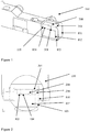
Figure 1 is a longitudinal cross-sectional perspective view of a positioning frame structure according to the present invention; -
Figure 2 is a traversal cross-sectional view of a positioning frame structure according to the present invention. - Referring to the figures, a positioning frame structure of the present invention will now be in detail described. The positioning frame structure of the present invention is used for the centering and positioning of an Integrated Chip (IC), especially the centering and positioning of an IC in small package on a large IC positioning magnet.
- Referring now to
figures 1 and 2 , which are a longitudinal cross-sectional perspective view and a traversal cross-sectional view of apositioning frame structure 100 according to the present invention, respectively. In thefigures 1 and 2 , thepositioning frame structure 100 generally comprises anIC carrier 101 and anIC positioning magnet 102. TheIC carrier 101 has afirst chamber 103 defined therein. In the illustrated embodiment, the cross section of thefirst chamber 103 is square in shape. However, it will be appreciated that thefirst chamber 103 can be any other suitable shape. - The
IC positioning magnet 102 is disposed within thefirst chamber 103 of theIC carrier 101. In embodiments, theIC positioning magnet 102 is sized to correspond to the size of thefirst chamber 103 of theIC carrier 101, so that theIC positioning magnet 102 can be fixedly disposed in thefirst chamber 103, and thus the centering and positioning between theIC positioning magnet 102 and theIC carrier 101 can be controlled and ensured. - The
positioning frame structure 100 according to the present invention is provided with anIC holder 300, which is disposed over theIC positioning magnet 102. In practice, anIC 200 is held in theIC holder 300, so that the centering and positioning of theIC 200 relative to theIC positioning magnet 102 can be obtained by means of theIC holder 300. - The size of the
IC positioning magnet 102 is larger than the size of theIC 200, so as to meet some special requirements in the field of chip package. Further, due to theIC holder 300, the size of theIC 200 can be very small, so as to overcome the drawback in prior art that the centering and positioning of the IC cannot be obtained if the IC is in small package. - The
IC holder 300 is provided with a receivingportion 301 and theIC 200 can be held in the receivingportion 301. The receivingportion 301 is sized and shaped to correspond to the size and shape of theIC 200, so that theIC 200 can be fixedly and removably disposed in the receivingportion 301. - The
IC carrier 101 is further provided with asecond chamber 104. Thesecond chamber 104 is located above thefirst chamber 103. - The
IC holder 300 is disposed within thesecond chamber 104 of theIC carrier 101. - The size of the
second chamber 104 is larger than the size of thefirst chamber 103. Ashoulder 105 is formed between thefirst chamber 103 and thesecond chamber 104. TheIC holder 300 abuts against theshoulder 105. - In a preferred embodiment, the outer periphery of the
IC holder 300 is sized to correspond to the size of thesecond chamber 104 of theIC carrier 101, so that theIC holder 300 can be fixedly and removably disposed within thesecond chamber 104. The centering and positioning between theIC 200 and theIC positioning magnet 102 is ensured by means of the structural relationship between theIC carrier 101, theIC positioning magnet 102 and theIC holder 300. - The
IC holder 300 and thesecond chamber 104 can be suitable shapes, for example, in the illustrated embodiment, thesecond chamber 104 has a cross section of symmetric hexagon, and theIC holder 300 has a cross section of corresponding symmetric hexagon, so as to generally conform to that of thesecond chamber 104. In the illustrated embodiment, a plurality of sides (which can be part or all of the sides) of theIC holder 300 abut against the corresponding inner sides of thesecond chamber 104, so that theIC holder 300 can be secured in place relative to thesecond chamber 104. - It is apparent for the skilled in the art that the
IC holder 300 and thesecond chamber 104 can be any other suitable shapes, as long as the centering and positioning between theIC 200 and theIC positioning magnet 102 can be ensured. - In addition, in order to further enhance the
IC 200 being secured in the receivingportion 301 of the IC holder, an additional securing means can be provided, for example, theIC 200 can be secured in the receivingportion 301 by means of a snap fit. - By means of the above solution, the positioning frame structure of the present invention can be used to control and thus ensure the centering and positioning of the IC and the positioning magnet on the carrier. Due to the present of the IC holder, the positioning magnet can be made to be larger than the IC. In this case, the present invention can be used for the operation of a smaller IC, i.e. the IC can be used in a small package. In addition, a large air gap can be obtained so as to facilitate the subsequent operation of the IC.
- Furthermore, without the operation using adhesive, the technical solution of the present invention saves the cost of operation as compared with the IC positioning manner in prior art.
- While the present invention has been described in detail by way of the above preferred embodiments, it is obvious to the skilled in the art that the present invention does not limit to the above embodiments. Changes can be made, as long as they are contained within the scope of the invention as defined by the claims.
Claims (5)
- A positioning frame structure, 100, for the centering and positioning of an integrated circuit (IC), 200, comprising a magnetic sensor, in which the positioning frame structure comprises:an IC carrier, 101, having a first chamber, 103, and a second chamber, 104;an IC holder, 300, configured to receive the IC; andan IC positioning magnet, 102,wherein the IC positioning magnet is disposed in the first chamber, and the IC holder is fixedly and removably disposed in the second chamber so that the IC holder is disposed above the IC positioning magnet disposed within the first chamber so as to center and position the IC relative to the IC positioning magnet,wherein a size of the IC positioning magnet is larger than a size of the IC,wherein a size of the second chamber is larger than a size of the first chamber,wherein the IC holder comprises a receiving portion, the IC being held in the receiving portion, the receiving portion being sized and shaped to correspond to the size and shape of the IC so that the IC can be fixedly disposed in the receiving portion,wherein the first chamber comprises an open top, and wherein the second chamber comprises:a bottom comprising a shoulder formed between the top of the first chamber and the circumference of the second chamber, the IC holder abutting against the shoulder;a circumference comprising a plurality of walls extending from an outer circumference of the shoulder; andan open top.
- The positioning frame structure according to claim 1, wherein first chamber includes a lower end and an upper end, the second chamber includes a lower end and an upper end, and the lower end of the second chamber is proximate to the upper end of the first chamber.
- The positioning frame structure according to claim 1, wherein the IC positioning magnet is sized to correspond to the size of the first chamber of the IC carrier, so that the IC positioning magnet can be fixedly disposed in the first chamber.
- The positioning frame structure according to claim 1, wherein the outer periphery of the IC holder is sized to correspond to the size of the second chamber of the IC carrier.
- The positioning frame structure according to claim 1, wherein the first chamber has a cross section which is square or rectangular in shape and/or the second chamber has a cross section which is square or rectangular in shape.
Applications Claiming Priority (1)
| Application Number | Priority Date | Filing Date | Title |
|---|---|---|---|
| CN201310752418.3A CN104749390B (en) | 2013-12-31 | 2013-12-31 | Positioning frame structure |
Publications (2)
| Publication Number | Publication Date |
|---|---|
| EP2896966A1 EP2896966A1 (en) | 2015-07-22 |
| EP2896966B1 true EP2896966B1 (en) | 2021-06-23 |
Family
ID=52423542
Family Applications (1)
| Application Number | Title | Priority Date | Filing Date |
|---|---|---|---|
| EP14200644.4A Active EP2896966B1 (en) | 2013-12-31 | 2014-12-30 | Positioning frame structure |
Country Status (5)
| Country | Link |
|---|---|
| US (1) | US9564351B2 (en) |
| EP (1) | EP2896966B1 (en) |
| JP (1) | JP6291412B2 (en) |
| KR (1) | KR20150079466A (en) |
| CN (1) | CN104749390B (en) |
Family Cites Families (47)
| Publication number | Priority date | Publication date | Assignee | Title |
|---|---|---|---|---|
| US2965235A (en) * | 1958-03-07 | 1960-12-20 | Daline Gordon | Perforated display panel with magnetic attachment means |
| DE8711744U1 (en) * | 1987-08-29 | 1988-12-29 | Heidelberger Druckmaschinen Ag, 6900 Heidelberg | Holding device for a hollow shaft incremental encoder |
| KR960000342B1 (en) * | 1989-03-14 | 1996-01-05 | 미쯔비시 덴끼 가부시끼가이샤 | Hall-efect sensor with integrally molded frame and plate supported hall element |
| JPH0344588A (en) * | 1989-07-12 | 1991-02-26 | Tdk Corp | Sensor for detecting moving object |
| US5007290A (en) * | 1989-10-31 | 1991-04-16 | New Sd, Inc | Method and apparatus for producing preload of an accelerometer assembly |
| US5115194A (en) * | 1990-09-27 | 1992-05-19 | Kearney-National Inc. | Hall effect position sensor with flux limiter and magnetic dispersion means |
| US5255795A (en) * | 1991-12-05 | 1993-10-26 | Vlsi Technology, Inc. | Test fixture |
| JPH07101163B2 (en) * | 1992-10-14 | 1995-11-01 | カーニー−ナショナル・インコーポレーテッド | Hall effect position sensor with magnetic flux limiter and magnetic dispersion means |
| US7876188B2 (en) * | 2006-11-06 | 2011-01-25 | Tang System | Green technologies: the killer application of EMI-free on-chip inductor |
| US5414355A (en) * | 1994-03-03 | 1995-05-09 | Honeywell Inc. | Magnet carrier disposed within an outer housing |
| JPH08139429A (en) * | 1994-11-07 | 1996-05-31 | Sumitomo Electric Ind Ltd | Electronic circuit device |
| US5500589A (en) * | 1995-01-18 | 1996-03-19 | Honeywell Inc. | Method for calibrating a sensor by moving a magnet while monitoring an output signal from a magnetically sensitive component |
| US5581179A (en) * | 1995-05-31 | 1996-12-03 | Allegro Microsystems, Inc. | Hall-effect ferrous-article-proximity sensor assembly |
| JPH09133743A (en) * | 1995-11-08 | 1997-05-20 | Murata Mfg Co Ltd | Magnetic sensor |
| US6355885B1 (en) * | 1996-05-02 | 2002-03-12 | William J. Rintz | Sub frame assembly for light switch assembly |
| WO1998054547A1 (en) * | 1997-05-29 | 1998-12-03 | Laboratorium Für Physikalische Elektronik | Magnetic rotation sensor |
| JPH11153452A (en) * | 1997-11-20 | 1999-06-08 | Hitachi Ltd | Rotation detection device |
| US6291990B1 (en) * | 1997-09-29 | 2001-09-18 | Hitachi, Ltd. | Revolution sensor |
| US6346811B1 (en) * | 1997-10-20 | 2002-02-12 | Wolff Controls Corp. | Methods for mounting a sensor and signal conditioner to form sensing apparatus having enhanced sensing capabilities and reduced size |
| US5868251A (en) * | 1997-11-06 | 1999-02-09 | Lin; Wan-Chang | Disk-shaped storage case for screwdriver tips |
| US6018130A (en) * | 1998-05-20 | 2000-01-25 | Breed Automotive Technology, Inc. | Roll-over sensor with pendulum mounted magnet |
| EP1407472A4 (en) * | 2001-06-28 | 2009-07-15 | Pollack Lab Inc | AUTONOMOUS DETECTION APPARATUS AND SYSTEM |
| US6707293B2 (en) * | 2001-11-15 | 2004-03-16 | Honeywell International Inc. | 360-degree rotary position sensor having a magnetoresistive sensor and a hall sensor |
| JP4179083B2 (en) * | 2003-07-08 | 2008-11-12 | 株式会社デンソー | Rotation detector |
| US7462317B2 (en) * | 2004-11-10 | 2008-12-09 | Enpirion, Inc. | Method of manufacturing an encapsulated package for a magnetic device |
| DE102005047414B4 (en) * | 2005-02-21 | 2012-01-05 | Infineon Technologies Ag | Magnetoresistive sensor module and method for producing the same |
| US7425824B2 (en) * | 2005-05-20 | 2008-09-16 | Honeywell International Inc. | Magnetoresistive sensor |
| JP4232771B2 (en) * | 2005-09-30 | 2009-03-04 | 株式会社デンソー | Rotation detector |
| US8701272B2 (en) * | 2005-10-05 | 2014-04-22 | Enpirion, Inc. | Method of forming a power module with a magnetic device having a conductive clip |
| FR2902872B1 (en) * | 2006-06-27 | 2008-11-14 | Arvinmeritor Light Vehicle Sys | DEVICE FOR MEASURING MAGNETIC FIELD. |
| US20080013298A1 (en) * | 2006-07-14 | 2008-01-17 | Nirmal Sharma | Methods and apparatus for passive attachment of components for integrated circuits |
| JP2008216043A (en) * | 2007-03-05 | 2008-09-18 | Honda Lock Mfg Co Ltd | Rotation sensor |
| US7570047B2 (en) * | 2007-06-18 | 2009-08-04 | Key Safety Systems, Inc. | Hall effect based angular position sensor |
| US7710110B2 (en) * | 2007-07-07 | 2010-05-04 | Honeywell International Inc. | Rotary sensor with rotary sensing element and rotatable hollow magnet |
| US7920042B2 (en) * | 2007-09-10 | 2011-04-05 | Enpirion, Inc. | Micromagnetic device and method of forming the same |
| US9518815B2 (en) * | 2008-08-06 | 2016-12-13 | Haas Automation, Inc. | Rotary position encoder for rotatable shafts |
| DE102009006529A1 (en) * | 2009-01-28 | 2010-08-26 | Continental Automotive Gmbh | position sensor |
| CN201681086U (en) * | 2010-05-11 | 2010-12-22 | 杭州南科汽车传感器有限公司 | Active wheel speed sensor |
| US9201123B2 (en) * | 2011-11-04 | 2015-12-01 | Infineon Technologies Ag | Magnetic sensor device and a method for fabricating the same |
| CN103094778A (en) * | 2011-11-04 | 2013-05-08 | 深圳富泰宏精密工业有限公司 | Portable electronic device and loading and unloading device for chip card thereof |
| US8727326B2 (en) * | 2012-03-21 | 2014-05-20 | Cheng Uei Precision Industry Co., Ltd. | Assembly jig |
| US8779635B2 (en) * | 2012-04-10 | 2014-07-15 | Kla-Tencor Corporation | Arrangement of reticle positioning device for actinic inspection of EUV reticles |
| DE102013219017A1 (en) * | 2012-12-20 | 2014-06-26 | Continental Teves Ag & Co. Ohg | Sensor for outputting an electrical signal |
| DE102012224424A1 (en) * | 2012-12-27 | 2014-07-17 | Robert Bosch Gmbh | Sensor system and cover device for a sensor system |
| US20140254835A1 (en) * | 2013-03-05 | 2014-09-11 | Analog Devices, Inc. | Packaged Microphone System with a Permanent Magnet |
| KR20160052728A (en) * | 2013-09-10 | 2016-05-12 | 케이에스알 아이피 홀딩스 엘엘씨. | Integrated brake control sensor |
| CN203772882U (en) * | 2013-12-31 | 2014-08-13 | 森萨塔科技(常州)有限公司 | Positioning framework structure |
-
2013
- 2013-12-31 CN CN201310752418.3A patent/CN104749390B/en active Active
-
2014
- 2014-12-26 JP JP2014263987A patent/JP6291412B2/en active Active
- 2014-12-29 US US14/584,207 patent/US9564351B2/en active Active
- 2014-12-30 KR KR1020140193614A patent/KR20150079466A/en not_active Withdrawn
- 2014-12-30 EP EP14200644.4A patent/EP2896966B1/en active Active
Non-Patent Citations (1)
| Title |
|---|
| None * |
Also Published As
| Publication number | Publication date |
|---|---|
| KR20150079466A (en) | 2015-07-08 |
| US20150187623A1 (en) | 2015-07-02 |
| EP2896966A1 (en) | 2015-07-22 |
| JP2015132601A (en) | 2015-07-23 |
| CN104749390B (en) | 2020-07-03 |
| JP6291412B2 (en) | 2018-03-14 |
| US9564351B2 (en) | 2017-02-07 |
| CN104749390A (en) | 2015-07-01 |
Similar Documents
| Publication | Publication Date | Title |
|---|---|---|
| KR101891347B1 (en) | Magnetic proximity sensor | |
| US20130200883A1 (en) | Magnetic field sensor | |
| TWI554742B (en) | Sensor device and encoder | |
| WO2013141981A3 (en) | Magnetic field sensor integrated circuit with integral ferromagnetic material | |
| JP2015078990A (en) | Magnetic field sensor and method for manufacturing the magnetic field sensor | |
| US20140076026A1 (en) | Relative humidity sensor | |
| WO2008120739A1 (en) | Torque detecting device | |
| US8803386B2 (en) | Brushless DC motor having structures for mounting a hall element and a magnetic ring outside a motor casing | |
| CN112393748B (en) | System with magnetic field shielding structure | |
| WO2009074582A3 (en) | Magnetic field sensor element | |
| US11125583B2 (en) | Integrated dual rotary position sensor | |
| US6703830B2 (en) | Tunable magnetic device for use in a proximity sensor | |
| US10416001B2 (en) | Magnet arrangement for rotational angle detection | |
| JP2011043345A (en) | Magnetic rotation detector | |
| US9564351B2 (en) | Positioning frame structure | |
| EP3489631B1 (en) | Mechanically powered scanning platform for sensors | |
| US20130235262A1 (en) | Method for packaging image sensor structure and image sensor structure formed from the same | |
| US20130082548A1 (en) | Switched reluctance motor | |
| CN204794577U (en) | Motor and drive arrangement | |
| CN208000319U (en) | Novel gear box velocity sensor | |
| WO2018053794A1 (en) | Rotary position sensor with dual magnet arrangement | |
| US20180359871A1 (en) | Housing to retain integrated circuit package | |
| CN106168476B (en) | Sensor assembly for a vehicle | |
| US11874298B2 (en) | Sensor devices with at least one bent connection conductor and methods for producing the sensor devices | |
| JPH11337369A (en) | Magnetic detector |
Legal Events
| Date | Code | Title | Description |
|---|---|---|---|
| PUAI | Public reference made under article 153(3) epc to a published international application that has entered the european phase |
Free format text: ORIGINAL CODE: 0009012 |
|
| 17P | Request for examination filed |
Effective date: 20141230 |
|
| AK | Designated contracting states |
Kind code of ref document: A1 Designated state(s): AL AT BE BG CH CY CZ DE DK EE ES FI FR GB GR HR HU IE IS IT LI LT LU LV MC MK MT NL NO PL PT RO RS SE SI SK SM TR |
|
| AX | Request for extension of the european patent |
Extension state: BA ME |
|
| 17P | Request for examination filed |
Effective date: 20160122 |
|
| RBV | Designated contracting states (corrected) |
Designated state(s): AL AT BE BG CH CY CZ DE DK EE ES FI FR GB GR HR HU IE IS IT LI LT LU LV MC MK MT NL NO PL PT RO RS SE SI SK SM TR |
|
| STAA | Information on the status of an ep patent application or granted ep patent |
Free format text: STATUS: EXAMINATION IS IN PROGRESS |
|
| 17Q | First examination report despatched |
Effective date: 20180528 |
|
| RIC1 | Information provided on ipc code assigned before grant |
Ipc: G01P 1/02 20060101AFI20201105BHEP Ipc: G01D 11/30 20060101ALI20201105BHEP Ipc: G01P 3/488 20060101ALI20201105BHEP Ipc: G01D 11/24 20060101ALI20201105BHEP |
|
| GRAP | Despatch of communication of intention to grant a patent |
Free format text: ORIGINAL CODE: EPIDOSNIGR1 |
|
| STAA | Information on the status of an ep patent application or granted ep patent |
Free format text: STATUS: GRANT OF PATENT IS INTENDED |
|
| INTG | Intention to grant announced |
Effective date: 20210119 |
|
| GRAS | Grant fee paid |
Free format text: ORIGINAL CODE: EPIDOSNIGR3 |
|
| GRAA | (expected) grant |
Free format text: ORIGINAL CODE: 0009210 |
|
| STAA | Information on the status of an ep patent application or granted ep patent |
Free format text: STATUS: THE PATENT HAS BEEN GRANTED |
|
| AK | Designated contracting states |
Kind code of ref document: B1 Designated state(s): AL AT BE BG CH CY CZ DE DK EE ES FI FR GB GR HR HU IE IS IT LI LT LU LV MC MK MT NL NO PL PT RO RS SE SI SK SM TR |
|
| REG | Reference to a national code |
Ref country code: GB Ref legal event code: FG4D |
|
| REG | Reference to a national code |
Ref country code: CH Ref legal event code: EP |
|
| REG | Reference to a national code |
Ref country code: DE Ref legal event code: R096 Ref document number: 602014078245 Country of ref document: DE Ref country code: AT Ref legal event code: REF Ref document number: 1404744 Country of ref document: AT Kind code of ref document: T Effective date: 20210715 |
|
| REG | Reference to a national code |
Ref country code: IE Ref legal event code: FG4D |
|
| REG | Reference to a national code |
Ref country code: LT Ref legal event code: MG9D |
|
| PG25 | Lapsed in a contracting state [announced via postgrant information from national office to epo] |
Ref country code: HR Free format text: LAPSE BECAUSE OF FAILURE TO SUBMIT A TRANSLATION OF THE DESCRIPTION OR TO PAY THE FEE WITHIN THE PRESCRIBED TIME-LIMIT Effective date: 20210623 Ref country code: BG Free format text: LAPSE BECAUSE OF FAILURE TO SUBMIT A TRANSLATION OF THE DESCRIPTION OR TO PAY THE FEE WITHIN THE PRESCRIBED TIME-LIMIT Effective date: 20210923 Ref country code: LT Free format text: LAPSE BECAUSE OF FAILURE TO SUBMIT A TRANSLATION OF THE DESCRIPTION OR TO PAY THE FEE WITHIN THE PRESCRIBED TIME-LIMIT Effective date: 20210623 Ref country code: FI Free format text: LAPSE BECAUSE OF FAILURE TO SUBMIT A TRANSLATION OF THE DESCRIPTION OR TO PAY THE FEE WITHIN THE PRESCRIBED TIME-LIMIT Effective date: 20210623 |
|
| REG | Reference to a national code |
Ref country code: AT Ref legal event code: MK05 Ref document number: 1404744 Country of ref document: AT Kind code of ref document: T Effective date: 20210623 |
|
| PG25 | Lapsed in a contracting state [announced via postgrant information from national office to epo] |
Ref country code: GR Free format text: LAPSE BECAUSE OF FAILURE TO SUBMIT A TRANSLATION OF THE DESCRIPTION OR TO PAY THE FEE WITHIN THE PRESCRIBED TIME-LIMIT Effective date: 20210924 Ref country code: LV Free format text: LAPSE BECAUSE OF FAILURE TO SUBMIT A TRANSLATION OF THE DESCRIPTION OR TO PAY THE FEE WITHIN THE PRESCRIBED TIME-LIMIT Effective date: 20210623 Ref country code: SE Free format text: LAPSE BECAUSE OF FAILURE TO SUBMIT A TRANSLATION OF THE DESCRIPTION OR TO PAY THE FEE WITHIN THE PRESCRIBED TIME-LIMIT Effective date: 20210623 Ref country code: RS Free format text: LAPSE BECAUSE OF FAILURE TO SUBMIT A TRANSLATION OF THE DESCRIPTION OR TO PAY THE FEE WITHIN THE PRESCRIBED TIME-LIMIT Effective date: 20210623 Ref country code: NO Free format text: LAPSE BECAUSE OF FAILURE TO SUBMIT A TRANSLATION OF THE DESCRIPTION OR TO PAY THE FEE WITHIN THE PRESCRIBED TIME-LIMIT Effective date: 20210923 |
|
| REG | Reference to a national code |
Ref country code: NL Ref legal event code: MP Effective date: 20210623 |
|
| PG25 | Lapsed in a contracting state [announced via postgrant information from national office to epo] |
Ref country code: AT Free format text: LAPSE BECAUSE OF FAILURE TO SUBMIT A TRANSLATION OF THE DESCRIPTION OR TO PAY THE FEE WITHIN THE PRESCRIBED TIME-LIMIT Effective date: 20210623 Ref country code: NL Free format text: LAPSE BECAUSE OF FAILURE TO SUBMIT A TRANSLATION OF THE DESCRIPTION OR TO PAY THE FEE WITHIN THE PRESCRIBED TIME-LIMIT Effective date: 20210623 Ref country code: RO Free format text: LAPSE BECAUSE OF FAILURE TO SUBMIT A TRANSLATION OF THE DESCRIPTION OR TO PAY THE FEE WITHIN THE PRESCRIBED TIME-LIMIT Effective date: 20210623 Ref country code: PT Free format text: LAPSE BECAUSE OF FAILURE TO SUBMIT A TRANSLATION OF THE DESCRIPTION OR TO PAY THE FEE WITHIN THE PRESCRIBED TIME-LIMIT Effective date: 20211025 Ref country code: ES Free format text: LAPSE BECAUSE OF FAILURE TO SUBMIT A TRANSLATION OF THE DESCRIPTION OR TO PAY THE FEE WITHIN THE PRESCRIBED TIME-LIMIT Effective date: 20210623 Ref country code: SK Free format text: LAPSE BECAUSE OF FAILURE TO SUBMIT A TRANSLATION OF THE DESCRIPTION OR TO PAY THE FEE WITHIN THE PRESCRIBED TIME-LIMIT Effective date: 20210623 Ref country code: SM Free format text: LAPSE BECAUSE OF FAILURE TO SUBMIT A TRANSLATION OF THE DESCRIPTION OR TO PAY THE FEE WITHIN THE PRESCRIBED TIME-LIMIT Effective date: 20210623 Ref country code: EE Free format text: LAPSE BECAUSE OF FAILURE TO SUBMIT A TRANSLATION OF THE DESCRIPTION OR TO PAY THE FEE WITHIN THE PRESCRIBED TIME-LIMIT Effective date: 20210623 Ref country code: CZ Free format text: LAPSE BECAUSE OF FAILURE TO SUBMIT A TRANSLATION OF THE DESCRIPTION OR TO PAY THE FEE WITHIN THE PRESCRIBED TIME-LIMIT Effective date: 20210623 |
|
| PG25 | Lapsed in a contracting state [announced via postgrant information from national office to epo] |
Ref country code: PL Free format text: LAPSE BECAUSE OF FAILURE TO SUBMIT A TRANSLATION OF THE DESCRIPTION OR TO PAY THE FEE WITHIN THE PRESCRIBED TIME-LIMIT Effective date: 20210623 |
|
| REG | Reference to a national code |
Ref country code: DE Ref legal event code: R097 Ref document number: 602014078245 Country of ref document: DE |
|
| PG25 | Lapsed in a contracting state [announced via postgrant information from national office to epo] |
Ref country code: DK Free format text: LAPSE BECAUSE OF FAILURE TO SUBMIT A TRANSLATION OF THE DESCRIPTION OR TO PAY THE FEE WITHIN THE PRESCRIBED TIME-LIMIT Effective date: 20210623 |
|
| PLBE | No opposition filed within time limit |
Free format text: ORIGINAL CODE: 0009261 |
|
| STAA | Information on the status of an ep patent application or granted ep patent |
Free format text: STATUS: NO OPPOSITION FILED WITHIN TIME LIMIT |
|
| 26N | No opposition filed |
Effective date: 20220324 |
|
| PG25 | Lapsed in a contracting state [announced via postgrant information from national office to epo] |
Ref country code: AL Free format text: LAPSE BECAUSE OF FAILURE TO SUBMIT A TRANSLATION OF THE DESCRIPTION OR TO PAY THE FEE WITHIN THE PRESCRIBED TIME-LIMIT Effective date: 20210623 |
|
| PG25 | Lapsed in a contracting state [announced via postgrant information from national office to epo] |
Ref country code: MC Free format text: LAPSE BECAUSE OF FAILURE TO SUBMIT A TRANSLATION OF THE DESCRIPTION OR TO PAY THE FEE WITHIN THE PRESCRIBED TIME-LIMIT Effective date: 20210623 Ref country code: IT Free format text: LAPSE BECAUSE OF FAILURE TO SUBMIT A TRANSLATION OF THE DESCRIPTION OR TO PAY THE FEE WITHIN THE PRESCRIBED TIME-LIMIT Effective date: 20210623 |
|
| REG | Reference to a national code |
Ref country code: CH Ref legal event code: PL |
|
| REG | Reference to a national code |
Ref country code: BE Ref legal event code: MM Effective date: 20211231 |
|
| PG25 | Lapsed in a contracting state [announced via postgrant information from national office to epo] |
Ref country code: LU Free format text: LAPSE BECAUSE OF NON-PAYMENT OF DUE FEES Effective date: 20211230 Ref country code: IE Free format text: LAPSE BECAUSE OF NON-PAYMENT OF DUE FEES Effective date: 20211230 |
|
| PG25 | Lapsed in a contracting state [announced via postgrant information from national office to epo] |
Ref country code: FR Free format text: LAPSE BECAUSE OF NON-PAYMENT OF DUE FEES Effective date: 20211231 Ref country code: BE Free format text: LAPSE BECAUSE OF NON-PAYMENT OF DUE FEES Effective date: 20211231 |
|
| PG25 | Lapsed in a contracting state [announced via postgrant information from national office to epo] |
Ref country code: LI Free format text: LAPSE BECAUSE OF NON-PAYMENT OF DUE FEES Effective date: 20211231 Ref country code: CH Free format text: LAPSE BECAUSE OF NON-PAYMENT OF DUE FEES Effective date: 20211231 |
|
| PG25 | Lapsed in a contracting state [announced via postgrant information from national office to epo] |
Ref country code: HU Free format text: LAPSE BECAUSE OF FAILURE TO SUBMIT A TRANSLATION OF THE DESCRIPTION OR TO PAY THE FEE WITHIN THE PRESCRIBED TIME-LIMIT; INVALID AB INITIO Effective date: 20141230 |
|
| PG25 | Lapsed in a contracting state [announced via postgrant information from national office to epo] |
Ref country code: CY Free format text: LAPSE BECAUSE OF FAILURE TO SUBMIT A TRANSLATION OF THE DESCRIPTION OR TO PAY THE FEE WITHIN THE PRESCRIBED TIME-LIMIT Effective date: 20210623 |
|
| P01 | Opt-out of the competence of the unified patent court (upc) registered |
Effective date: 20230708 |
|
| PG25 | Lapsed in a contracting state [announced via postgrant information from national office to epo] |
Ref country code: MK Free format text: LAPSE BECAUSE OF FAILURE TO SUBMIT A TRANSLATION OF THE DESCRIPTION OR TO PAY THE FEE WITHIN THE PRESCRIBED TIME-LIMIT Effective date: 20210623 |
|
| PG25 | Lapsed in a contracting state [announced via postgrant information from national office to epo] |
Ref country code: MT Free format text: LAPSE BECAUSE OF FAILURE TO SUBMIT A TRANSLATION OF THE DESCRIPTION OR TO PAY THE FEE WITHIN THE PRESCRIBED TIME-LIMIT Effective date: 20210623 |
|
| REG | Reference to a national code |
Ref country code: DE Ref legal event code: R081 Ref document number: 602014078245 Country of ref document: DE Owner name: QST SOLUTIONS LIMITED, SAN JOSE, US Free format text: FORMER OWNER: SENSATA TECHNOLOGIES (CHANGZHOU) CO., LTD, CHANGZHOU, JIANGSU, CN |
|
| REG | Reference to a national code |
Ref country code: GB Ref legal event code: 732E Free format text: REGISTERED BETWEEN 20250619 AND 20250625 |
|
| PG25 | Lapsed in a contracting state [announced via postgrant information from national office to epo] |
Ref country code: TR Free format text: LAPSE BECAUSE OF FAILURE TO SUBMIT A TRANSLATION OF THE DESCRIPTION OR TO PAY THE FEE WITHIN THE PRESCRIBED TIME-LIMIT Effective date: 20210623 |
|
| PGFP | Annual fee paid to national office [announced via postgrant information from national office to epo] |
Ref country code: GB Payment date: 20251218 Year of fee payment: 12 |
|
| PGFP | Annual fee paid to national office [announced via postgrant information from national office to epo] |
Ref country code: DE Payment date: 20251222 Year of fee payment: 12 |