EP2894755A1 - Contactless charging system - Google Patents
Contactless charging system Download PDFInfo
- Publication number
- EP2894755A1 EP2894755A1 EP13833654.0A EP13833654A EP2894755A1 EP 2894755 A1 EP2894755 A1 EP 2894755A1 EP 13833654 A EP13833654 A EP 13833654A EP 2894755 A1 EP2894755 A1 EP 2894755A1
- Authority
- EP
- European Patent Office
- Prior art keywords
- power
- power transmission
- state
- power receiving
- carrier
- Prior art date
- Legal status (The legal status is an assumption and is not a legal conclusion. Google has not performed a legal analysis and makes no representation as to the accuracy of the status listed.)
- Granted
Links
- 230000005540 biological transmission Effects 0.000 claims abstract description 118
- 238000001514 detection method Methods 0.000 claims abstract description 76
- 230000005674 electromagnetic induction Effects 0.000 claims abstract description 7
- 238000007599 discharging Methods 0.000 claims description 13
- 230000006870 function Effects 0.000 description 10
- 238000010586 diagram Methods 0.000 description 6
- 239000003990 capacitor Substances 0.000 description 4
- 230000001276 controlling effect Effects 0.000 description 4
- 235000014676 Phragmites communis Nutrition 0.000 description 3
- 230000001413 cellular effect Effects 0.000 description 3
- 239000002699 waste material Substances 0.000 description 3
- 230000000694 effects Effects 0.000 description 2
- HBBGRARXTFLTSG-UHFFFAOYSA-N Lithium ion Chemical compound [Li+] HBBGRARXTFLTSG-UHFFFAOYSA-N 0.000 description 1
- 229910001416 lithium ion Inorganic materials 0.000 description 1
- 230000001105 regulatory effect Effects 0.000 description 1
Images


Classifications
-
- H—ELECTRICITY
- H02—GENERATION; CONVERSION OR DISTRIBUTION OF ELECTRIC POWER
- H02J—CIRCUIT ARRANGEMENTS OR SYSTEMS FOR SUPPLYING OR DISTRIBUTING ELECTRIC POWER; SYSTEMS FOR STORING ELECTRIC ENERGY
- H02J50/00—Circuit arrangements or systems for wireless supply or distribution of electric power
- H02J50/10—Circuit arrangements or systems for wireless supply or distribution of electric power using inductive coupling
- H02J50/12—Circuit arrangements or systems for wireless supply or distribution of electric power using inductive coupling of the resonant type
-
- H—ELECTRICITY
- H02—GENERATION; CONVERSION OR DISTRIBUTION OF ELECTRIC POWER
- H02J—CIRCUIT ARRANGEMENTS OR SYSTEMS FOR SUPPLYING OR DISTRIBUTING ELECTRIC POWER; SYSTEMS FOR STORING ELECTRIC ENERGY
- H02J50/00—Circuit arrangements or systems for wireless supply or distribution of electric power
- H02J50/80—Circuit arrangements or systems for wireless supply or distribution of electric power involving the exchange of data, concerning supply or distribution of electric power, between transmitting devices and receiving devices
-
- H—ELECTRICITY
- H02—GENERATION; CONVERSION OR DISTRIBUTION OF ELECTRIC POWER
- H02J—CIRCUIT ARRANGEMENTS OR SYSTEMS FOR SUPPLYING OR DISTRIBUTING ELECTRIC POWER; SYSTEMS FOR STORING ELECTRIC ENERGY
- H02J7/00—Circuit arrangements for charging or depolarising batteries or for supplying loads from batteries
- H02J7/00032—Circuit arrangements for charging or depolarising batteries or for supplying loads from batteries characterised by data exchange
- H02J7/00034—Charger exchanging data with an electronic device, i.e. telephone, whose internal battery is under charge
Definitions
- the present invention relates to a contactless charging system that transmits electric power in a contactless manner through electromagnetic induction to charge a secondary battery built in a power receiving side, and more particularly to a function of switching between the state during charging of the secondary battery and the state during discharging where electric power is supplied from the secondary battery.
- a contactless charging system is comprised of a power transmission module incorporated in a charger, for example, and a power receiving module incorporated in a set device. Electric power is transmitted from the power transmission module to the power receiving module through electromagnetic induction between a power transmission coil of the power transmission module and a power receiving coil of the power receiving module. In the power receiving module, high-frequency power received by the power receiving coil is converted to DC power, and voltage-converted to a charging voltage, to perform charging of a secondary battery.
- Patent Document 1 discloses a configuration, as an example of a contactless charging system, where full charge of a battery in a load section as the power receiving side is detected and the operation mode is switched according to the detection result. More specifically, full charge is detected based on a voltage change appearing in a primary coil along with a load change in a secondary coil of the load section that occurs due to full charge. In response to this detection, control is performed to stop power transmission from a power source section as the primary side to the load section.
- Patent Documents 1 to 4 merely disclose a configuration of controlling the power transmission operation on the power transmission side in response to detection of full charge, and include no disclosure on a configuration of controlling an operation related to a secondary battery on the power receiving side. That is, the controls disclosed in Patent Documents 1 to 4 do not involve control of stopping power supply to a small device during charging of the secondary battery and permitting switching to the power supply state where normal power supply is performed in response to detection of full charge.
- Patent Documents 1 to 4 describes control of switching between the power shutdown state and the power supply state according to whether or not the power receiving module is loaded in a predetermined power receiving position of the power transmission module.
- an objective of the present invention is providing a contactless charging system where switching between the power shutdown state where power supply by discharging of a secondary battery is stopped and the power supply state where power supply is permitted is controlled according to the detection result on whether or not a power receiving module is loaded on a power transmitting module.
- the contactless charging system includes, as basic components: a power transmission module having a power transmission coil for transmitting high-frequency power; and a power receiving module having a power receiving coil that receives the high-frequency power through electromagnetic induction and a secondary battery charged with DC power obtained by rectifying the received power.
- the power receiving module includes a switching control section that performs switching between a power shutdown state where power supply by discharging of the secondary battery is stopped and a power supply state where power supply by discharging of the secondary battery is permitted, and a carrier detection circuit that generates a SW signal the ON/OFF of which is switched according to the presence or absence of a power receiving carrier of the high-frequency power in the power receiving coil, and the switching control section controls the switching to the power shutdown state when the SW signal indicates the presence of the power receiving carrier, and to the power supply state when the SW signal indicates the absence of the power receiving carrier.
- the power receiving module includes a switching control section that performs switching between a power shutdown state where power supply by discharging of the secondary battery is stopped and a power supply state where power supply by discharging of the secondary battery is permitted, and a loading detection section that detects a state where the power receiving module is loaded in a predetermined power receiving position with respect to the power transmission module and outputs a loading detection signal, and the switching control section controls the switching to the power shutdown state when the loading detection signal is being output, and switching to the power supply state when the loading detection signal is not output.
- the loaded state of the power receiving module on the power transmission module is determined according to the presence or absence of detection of the power receiving carrier by the carrier detection circuit, to control switching between the power shutdown state and the power supply state by the switching control section.
- this control an occurrence of permitting discharge even though the set device is not put to normal use is avoided, and this is effective for preventing waste of stored energy of a small-capacity secondary battery.
- switching between the power shutdown state and the power supply state by the switching control section is controlled according to the loaded state of the power receiving module on the power transmission module based on the loading detection signal from the loading detection section. With this control, an effect similar to that in the first configuration is obtained.
- the contactless charging system according to the present invention can take the following forms based on the above-described configurations.
- the power receiving module may include a charged state detection section that detects whether or not the secondary battery is in a fully charged state and outputs a charge detection signal and a transmitter section that transmits data including the charge detection signal
- the power transmission module may include a receiver section that receives transmitted data from the transmitter section of the power receiving module and a power transmission control circuit that switches the level of a power transmission carrier of the high-frequency power supplied to the power transmission coil between a normal power transmission level and a reduced level lower than the normal power transmission level
- the power transmission control circuit may control the level of the power transmission carrier to the normal power transmission level when the charge detection signal received by the receiver section indicates a state that is not the fully charged state, and to the reduced level when it indicates the fully charged state.
- the power receiving module may include a charged state detection section that detects whether or not the secondary battery is in a fully charged state and outputs a charge detection signal and a transmitter section that transmits data including the charge detection signal
- the power transmission module may include a receiver section that receives transmitted data from the transmitter section of the power receiving module and a power transmission control circuit that switches the level of a power transmission carrier of the high-frequency power supplied to the power transmission coil between a normal power transmission level and a power transmission stop level
- the power transmission control circuit may control the level of the power transmission carrier to the normal power transmission level when the charge detection signal received by the receiver section indicates a state that is not the fully charged state, and to the power transmission stop level when it indicates the fully charged state.
- the loading detection section may be comprised of a proximity switch
- the power transmission module may include a switching action section placed next to the power receiving position of the power receiving module
- the proximity switch may be switched by the switching action section in a state where the power receiving module is placed in the power receiving position to generate the loading detection signal.
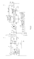
- a contactless charging system of Embodiment 1 will be described with reference to the block diagram shown in FIG. 1 .
- This system is configured to transmit electric power between a power transmission coil 2 of a power transmission module 1 and a power receiving coil 4 of a power receiving module 3 through electromagnetic induction.
- the power transmission module 1 is incorporated in a charger, and the power receiving module 3 is incorporated in a set device such as a cellular phone and a hearing assist.
- High-frequency power is supplied from a coil driver 6 to a resonant circuit constituted by the power transmission coil 2 and a resonant capacitor 5, to perform power transmission from the power transmission coil 2.
- the operation of the coil driver 6 is controlled by a power transmission control circuit 7.
- the high-frequency power is received by a resonant circuit constituted by a parallel circuit of the power receiving coil 4 and a resonant capacitor 8.
- An AC voltage at both ends of the resonant capacitor 8 is supplied to a rectifying circuit 9 to be converted to a DC voltage.
- the output power of the rectifying circuit 9 is regulated to a fixed voltage by a regulator 10, and then supplied to a secondary battery 12 via control by a charging control circuit 11.
- the charging control circuit 11 is configured to have a function as a protection circuit for the secondary battery 12 although illustration is omitted, in addition to the function of charging control for the secondary battery 12.
- Discharged power from the secondary battery 12 is supplied to a power source section 15 of the set device incorporating the power receiving module 3 via an output switch 13. Therefore, when the output switch 13 is OFF, the set device is put in the power shutdown state where power supply by discharging of the secondary battery 12 is stopped.
- the output switch 13 is ON, it is put in the power supply state where power supply by discharging of the secondary battery 12 is permitted.
- a carrier detection circuit 14 is also connected to the output side of the rectifying circuit 9.
- the carrier detection circuit 14 detects the presence or absence of a carrier of high-frequency power in the power receiving coil 4, and generates a SW signal the ON/OFF of which is switched according to the presence or absence of the power receiving carrier.
- the ON/OFF of the output switch 13 is controlled with the SW signal.
- FIG. 2 shows correspondences among the waveform of the carrier signal (a) of high-frequency power in the power receiving coil 4, the waveform of the SW signal (b) output by the carrier detection circuit 14, and the time periods of a charge mode and a discharge mode.
- the time period when a carrier waveform 16 is present in the carrier signal (a) corresponds to the charge mode
- the time period when the carrier waveform 16 is absent corresponds to the discharge mode.
- the SW signal (b) is switched according to the waveform of the carrier signal (a): it has a waveform of being OFF during the time period when the carrier waveform 16 is present (charge mode) and ON during the time period when the carrier waveform 16 is absent (discharge mode).
- the carrier detection circuit 14 constitutes the switching control section together with the output switch 13 by controlling the output switch 13 with the ON/OFF of the SW signal. More specifically, the output switch 13 is controlled to be OFF with the SW signal being OFF, and while the power shutdown state is maintained, the secondary battery 12 is charged (charge mode). By contrast, the output switch 13 is turned ON with the SW signal being ON, to be controlled to the power supply state (discharge mode).
- the power receiving module 3 in a situation where a carrier is being sent to the power receiving coil 4, it is determined that the power receiving module 3 is loaded on the power transmission module 1, i.e., the charger, so that the state is controlled to the power shutdown state.
- the power receiving module 3 has been removed from the charger, so that the state is controlled to the power supply state.
- control according to the detection result on whether or not the power receiving module 3 is loaded in the power receiving position is virtually performed.
- This function is effective for preventing waste of stored energy of a small-capacity secondary battery, and thus advantageous for a small set device, in particular.
- a contactless charging system of Embodiment 2 will be described with reference to the block diagram shown in FIG. 3 .
- the basic configuration of this system is similar to that of Embodiment 1, where like components are denoted by the same reference characters, and repetition of description is omitted.
- the power receiving module 3 is provided with a charged state detection section that detects whether or not the secondary battery 12 is fully charged and outputs a charge detection signal and a transmitter section that transmits data including the charge detection signal.
- the charged state detection section is configured as part of the function of a control/data generation circuit 20. More specifically, the control/data generation circuit 20 generates the charge detection signal based on control data supplied from the charging control circuit 11, and supplies the signal to a modulation circuit 21.
- the transmitter section which is constituted by the modulation circuit 21 and a load modulation section 22, transmits data including the charge detection signal supplied from the control/data generation circuit 20 via the power receiving coil 4.
- the power transmission module 1 is provided with a receiver section 23 that receives transmitted data from the transmitter section (21, 22) of the power receiving module 3.
- the power transmission control circuit 24 has a function of controlling the coil driver 6 based on the charge detection signal received by the receiver section 23. More specifically, the power transmission control circuit 24 switches the level of the power transmission carrier of high-frequency power supplied by the coil driver 6 between a normal power transmission level and a reduced level lower than the normal power transmission level. This switching is performed based on the charge detection signal received by the receiver section 23, where the level of the power transmission carrier is controlled to the normal power transmission level when the fully charged state is not attained, and to the reduced level when the fully charged state is attained.
- FIG. 4 shows correspondences among the waveform of the carrier signal (a) of high-frequency power in the power receiving coil 4, the waveform of the SW signal (b) output by the carrier detection circuit 14, and the time periods of the charge mode, a standby mode, and the discharge mode.
- the carrier signal (a) there appear a transmission-time carrier waveform 25 indicating the carrier of the normal power transmission level and a reduced carrier waveform 26 indicating the carrier of the reduced level.
- the time period when the transmission-time carrier waveform 25 is present in the carrier signal (a) corresponds to the charge mode, and the time period when the reduced carrier waveform 26 is present corresponds to the standby mode.
- the time period when no carrier waveform is present corresponds to the discharge mode.
- a charge detection signal 27 indicating attainment of full charge appears in a tail portion of the transmission-time carrier waveform 25 in the carrier signal (a).
- the charge detection signal 27 is one transmitted from the power receiving module 3 to the power transmission module 1 by load modulation.
- the power transmission control circuit 24 switches the power transmission carrier from the normal power transmission level to the reduced level by receiving the charge detection signal 27, whereby the reduced carrier waveform 26 is generated.
- the SW signal (b) is switched according to the waveform of the carrier signal (a): it has a waveform of being OFF during the time period when the transmission-time carrier waveform 25 or the reduced carrier waveform 26 is present (charge mode, standby mode) and ON during the time period when no carrier waveform is present (discharge mode).
- the carrier detection circuit 14 controls the output switch 13 with the ON/OFF of the SW signal, and constitutes the switching control section together with the output switch 13.
- the output switch 13 is controlled to be OFF with the SW signal being OFF, to maintain the power shutdown state.
- the charge mode or the standby mode is established according to the state of the carrier signal (a).
- the charge mode charging of the secondary battery 12 is performed with the carrier of the normal power transmission level.
- the standby mode no charging is performed since the transmitted power from the power transmission module 1 is reduced to the reduced level.
- the output switch 13 is turned ON with the ON state of the SW signal, and the state is controlled to the power supply state (discharge mode).
- the output switch 13 will not be switched to ON. There will be no charging once full charge is attained, but since the carrier of the reduced level is detected, the mode moves to the standby mode with no switching of the output switch 13 to ON. Therefore, a function of preventing automatic switching to the normal operation as long as the power receiving module 3 is receiving a carrier is obtained.
- control according to the detection result on whether or not the power receiving module 3 is loaded in the power receiving position is performed. Therefore, in a situation where the power receiving module 3 is loaded in the power receiving position, an occurrence of permitting discharge even though the set device is not put to normal use is avoided. Moreover, once the fully charged state is attained, the mode moves to the standby mode, whereby power consumption can be reduced.
- a contactless charging system of Embodiment 3 will be described with reference to the block diagram shown in FIG. 5 .
- the basic configuration of this system is similar to that of Embodiment 2, where like components are denoted by the same reference characters, and repetition of description is omitted.
- This embodiment is characterized in having a proximity switch 28 in place of the carrier detection circuit 14 in the power receiving module 3 in Embodiment 2.
- the proximity switch 28 constitutes the loading detection section for detecting the loaded state of the power receiving module 3 with respect to the power transmission module 1.
- the proximity switch 28 switches to ON or OFF according to whether or not the power receiving module 3 is loaded in the predetermined power receiving position with respect to the power transmission module 1. It is herein assumed that the ON state corresponds to the loaded state in the power receiving position. A voltage corresponding to the ON/OFF of the proximity switch 28 is supplied to the control/data generation circuit 20.
- the control/data generation circuit 20 generates the SW signal by associating the ON state of the proximity switch 28 with a loading detection signal (signal indicating detection of the loaded state of the power receiving module 3 in the power receiving position) to control the output switch 13.
- the ON/OFF of the proximity switch 28 is switched by a switching action section provided in the power transmission module 1. More specifically, switching of the proximity switch 28 is performed by the action of the switching action section according to the loading/unloading of the power receiving module 3 on/from the power transmission module 1.
- a reed switch controlled in response to magnetic force can be used, for example.
- a magnet may be placed in the power transmission module 1 next to the power receiving position of the power receiving module 3.
- a mechanical reed switch may be used as the proximity switch 28.
- a pressing member for switching the ON/OFF of the mechanical reed switch may be provided in the power transmission module 1.
- the proximity switch 28 may be configured of a combination of a light source and a photosensor.
- the loading detection signal corresponds to the state where a carrier waveform is present in the carrier signal in Embodiment 2. Therefore, the SW signal output by the control/data generation circuit 20 is OFF when the loading detection signal is being output and ON when this signal is not supplied. That is, as in Embodiment 2, the OFF state of the SW signal corresponds to the state where the power receiving module 3 is loaded on the power transmission module 1 (charger), and the ON state of the SW signal corresponds to the state where the power receiving module 3 is not loaded on the power transmission module 1.
- the way of the control of the coil driver 6 by the power transmission control circuit 24 based on the charge detection signal received by the receiver section 23 is different from that in Embodiment 2. That is, the power transmission control circuit 24 performs switching between the state where the carrier of high-frequency power of the normal power transmission level is supplied from the coil driver 6 and the state where the output of the carrier of high-frequency power is stopped. This switching is performed so that the carrier of the normal power transmission level is output when the charge detection signal does not indicate the fully charged state and the output of the carrier is stopped when it indicates the fully charged state.
- FIG. 6 shows correspondences among the waveform of the carrier signal (a), the waveform of the SW signal (b) output by the control/data generation circuit 20, and the time periods of the charge mode, the standby mode, and the discharge mode.
- the time period when a transmission-time carrier waveform 29 is present in the carrier signal (a) corresponds to the charge mode.
- a charge detection signal 30 indicating attainment of full charge is included in a tail portion of the transmission-time carrier waveform 29.
- the power transmission control circuit 24 stops the output of the power transmission carrier of high-frequency power by receiving the charge detection signal 30. Once the output of the power transmission carrier is stopped, the transmission-time carrier waveform 29 disappears from the waveform of the carrier signal (a).
- the time period when the SW signal (b) is OFF and the transmission-time carrier waveform 29 is absent corresponds to the standby mode.
- the OFF period of the SW signal (b) occurs with the output of the loading detection signal from the proximity switch 28. Therefore, during the OFF period of the SW signal (b), the power shutdown state is maintained irrespective of the state of the carrier signal (a). At the same time, as described above, the charge mode or the standby mode is established according to the state of the carrier signal (a). During the ON period of the SW signal (b), the output switch 13 is turned ON, and the state is controlled to the power supply state (discharge mode).
- the power shutdown state is maintained, and charging of the secondary battery 12 with the carrier of the normal power transmission level is performed.
- the standby mode while the transmission-time carrier waveform 29 disappears from the waveform of the carrier signal (a), the SW signal (b) is OFF with the ON output of the proximity switch 28. Therefore, although transmission of the carrier from the power transmission module 1 is stopped, the power shutdown state is maintained.
- the loading detection signal is generated from the proximity switch 28 when the power receiving module 3 is kept loaded on the power transmission module 1, and the mode moves to the standby mode.
- a function of preventing automatic switching to the normal operation even though the output of the power transmission carrier is stopped is obtained. Therefore, an occurrence of permitting discharge even though the set device is not put to normal use is avoided.
- the mode moves to the standby mode, whereby power consumption can be reduced.
- the configuration is made so that the output of the proximity switch 28 controls the ON/OFF of the output switch 13 via the control/data generation circuit 20.
- the output switch 13 may be formed of the proximity switch 28, and the proximity switch 28 may be made to also function as the switching control section.
- the proximity switch 28 as the loading detection section is integrated with the output switch 13 as the switching control section is possible.
- the contactless charging system according to the present invention in which the power shutdown state and the power supply state are switched to each other according to the loaded state of the power receiving module on the power transmission module, is effective for preventing waste of stored energy of a small-capacity secondary battery and thus useful for small electrical devices such as cellular phones and hearing aids.
Abstract
Description
- The present invention relates to a contactless charging system that transmits electric power in a contactless manner through electromagnetic induction to charge a secondary battery built in a power receiving side, and more particularly to a function of switching between the state during charging of the secondary battery and the state during discharging where electric power is supplied from the secondary battery.
- In recent years, a contactless power transmission system that feeds power in a contactless manner (wirelessly) has been increasingly used for small electrical devices such as cellular phones. With use of a charging system employing contactless power transmission for charging a secondary battery built in a small electrical device, cumbersome charging operation is widely improved. Also, for a small set device, such as a hearing aid, operating with a button lithium ion battery, which often has to be waterproof considering its use environment, contactless charging of the battery is essential from the standpoint of the form.
- A contactless charging system is comprised of a power transmission module incorporated in a charger, for example, and a power receiving module incorporated in a set device. Electric power is transmitted from the power transmission module to the power receiving module through electromagnetic induction between a power transmission coil of the power transmission module and a power receiving coil of the power receiving module. In the power receiving module, high-frequency power received by the power receiving coil is converted to DC power, and voltage-converted to a charging voltage, to perform charging of a secondary battery.
- In a small set device as that described above, which uses a button secondary battery small in capacity, it is necessary to make effective use of stored energy at the time of contactless charging. Therefore, during charging operation for the secondary battery, it is desirable to control the set device into a power shutdown state where normal power supply to the set device by discharging of the secondary battery is stopped. Switching to a power supply state where normal power supply to the set device is permitted may be made possible after attainment of full charge is detected.
- It is also desirable to perform control not to switch the state to the power supply state in a situation where the power receiving module is loaded in a predetermined power receiving position of the power transmission module even though attainment of full charge is detected. This is because it is often unnecessary to assume a situation where the set device is put to normal use while being loaded on the power transmission module. Therefore, it is desirable to control switching between the power shutdown state and the power supply state according to whether or not the power receiving module is loaded on the power transmission module.
- It is however difficult from the structural standpoint to provide a function of switching the operation manually in a small set device such as a hearing aid, and also this makes the handling cumbersome. Therefore, a configuration is necessary where the loaded state of the power receiving module is made detectable and switching between the power shutdown state and the power supply state is performed according to the detected result.
-
Patent Document 1 discloses a configuration, as an example of a contactless charging system, where full charge of a battery in a load section as the power receiving side is detected and the operation mode is switched according to the detection result. More specifically, full charge is detected based on a voltage change appearing in a primary coil along with a load change in a secondary coil of the load section that occurs due to full charge. In response to this detection, control is performed to stop power transmission from a power source section as the primary side to the load section. - Also, in contactless charging systems described in
Patent Documents 2 to 4, a configuration is disclosed where normal power transmission for charging from the power transmission side is stopped once full charge is attained, and an operation for checking whether or not restart of normal power transmission is necessary is repeated intermittently. -
- [Patent Document 1]
JP H06-339232A - [Patent Document 2]
JP 2008-178195A - [Patent Document 3]
JP 2008-236968A - [Patent Document 4]
JP 2010-35417A -
Patent Documents 1 to 4 merely disclose a configuration of controlling the power transmission operation on the power transmission side in response to detection of full charge, and include no disclosure on a configuration of controlling an operation related to a secondary battery on the power receiving side. That is, the controls disclosed inPatent Documents 1 to 4 do not involve control of stopping power supply to a small device during charging of the secondary battery and permitting switching to the power supply state where normal power supply is performed in response to detection of full charge. - It is needless to mention that none of
Patent Documents 1 to 4 describes control of switching between the power shutdown state and the power supply state according to whether or not the power receiving module is loaded in a predetermined power receiving position of the power transmission module. - In view of the above, an objective of the present invention is providing a contactless charging system where switching between the power shutdown state where power supply by discharging of a secondary battery is stopped and the power supply state where power supply is permitted is controlled according to the detection result on whether or not a power receiving module is loaded on a power transmitting module.
- The contactless charging system according to the present invention includes, as basic components: a power transmission module having a power transmission coil for transmitting high-frequency power; and a power receiving module having a power receiving coil that receives the high-frequency power through electromagnetic induction and a secondary battery charged with DC power obtained by rectifying the received power.
- To solve the above-described problem, in the contactless charging system of the first configuration according to the invention, the power receiving module includes a switching control section that performs switching between a power shutdown state where power supply by discharging of the secondary battery is stopped and a power supply state where power supply by discharging of the secondary battery is permitted, and a carrier detection circuit that generates a SW signal the ON/OFF of which is switched according to the presence or absence of a power receiving carrier of the high-frequency power in the power receiving coil, and the switching control section controls the switching to the power shutdown state when the SW signal indicates the presence of the power receiving carrier, and to the power supply state when the SW signal indicates the absence of the power receiving carrier.
- In the contactless charging system of the second configuration according to the invention, the power receiving module includes a switching control section that performs switching between a power shutdown state where power supply by discharging of the secondary battery is stopped and a power supply state where power supply by discharging of the secondary battery is permitted, and a loading detection section that detects a state where the power receiving module is loaded in a predetermined power receiving position with respect to the power transmission module and outputs a loading detection signal, and the switching control section controls the switching to the power shutdown state when the loading detection signal is being output, and switching to the power supply state when the loading detection signal is not output.
- According to the contactless charging system of the first configuration described above, the loaded state of the power receiving module on the power transmission module is determined according to the presence or absence of detection of the power receiving carrier by the carrier detection circuit, to control switching between the power shutdown state and the power supply state by the switching control section. With this control, an occurrence of permitting discharge even though the set device is not put to normal use is avoided, and this is effective for preventing waste of stored energy of a small-capacity secondary battery.
- According to the contactless charging system of the second configuration, switching between the power shutdown state and the power supply state by the switching control section is controlled according to the loaded state of the power receiving module on the power transmission module based on the loading detection signal from the loading detection section. With this control, an effect similar to that in the first configuration is obtained.
-
- [
FIG. 1] FIG. 1 is a block diagram showing a contactless charging system ofEmbodiment 1. - [
FIG. 2] FIG. 2 is a waveform chart for explaining the operation of the contactless charging system ofEmbodiment 1. - [
FIG. 3] FIG. 3 is a block diagram showing a contactless charging system ofEmbodiment 2. - [
FIG. 4] FIG. 4 is a waveform chart for explaining the operation of the contactless charging system ofEmbodiment 2. - [
FIG. 5] FIG. 5 is a block diagram showing a contactless charging system ofEmbodiment 3. - [
FIG. 6] FIG. 6 is a waveform chart for explaining the operation of the contactless charging system ofEmbodiment 3. - The contactless charging system according to the present invention can take the following forms based on the above-described configurations.
- That is, in the contactless charging system of the first configuration, the power receiving module may include a charged state detection section that detects whether or not the secondary battery is in a fully charged state and outputs a charge detection signal and a transmitter section that transmits data including the charge detection signal, the power transmission module may include a receiver section that receives transmitted data from the transmitter section of the power receiving module and a power transmission control circuit that switches the level of a power transmission carrier of the high-frequency power supplied to the power transmission coil between a normal power transmission level and a reduced level lower than the normal power transmission level, and the power transmission control circuit may control the level of the power transmission carrier to the normal power transmission level when the charge detection signal received by the receiver section indicates a state that is not the fully charged state, and to the reduced level when it indicates the fully charged state.
- In the contactless charging system of the second configuration, the power receiving module may include a charged state detection section that detects whether or not the secondary battery is in a fully charged state and outputs a charge detection signal and a transmitter section that transmits data including the charge detection signal, the power transmission module may include a receiver section that receives transmitted data from the transmitter section of the power receiving module and a power transmission control circuit that switches the level of a power transmission carrier of the high-frequency power supplied to the power transmission coil between a normal power transmission level and a power transmission stop level, and the power transmission control circuit may control the level of the power transmission carrier to the normal power transmission level when the charge detection signal received by the receiver section indicates a state that is not the fully charged state, and to the power transmission stop level when it indicates the fully charged state.
- The loading detection section may be comprised of a proximity switch, the power transmission module may include a switching action section placed next to the power receiving position of the power receiving module, and the proximity switch may be switched by the switching action section in a state where the power receiving module is placed in the power receiving position to generate the loading detection signal.
- Embodiments of the present invention will be described hereinafter with reference to the accompanying drawings.
- A contactless charging system of
Embodiment 1 will be described with reference to the block diagram shown inFIG. 1 . This system is configured to transmit electric power between apower transmission coil 2 of apower transmission module 1 and a power receiving coil 4 of apower receiving module 3 through electromagnetic induction. Thepower transmission module 1 is incorporated in a charger, and thepower receiving module 3 is incorporated in a set device such as a cellular phone and a hearing assist. - High-frequency power is supplied from a
coil driver 6 to a resonant circuit constituted by thepower transmission coil 2 and aresonant capacitor 5, to perform power transmission from thepower transmission coil 2. The operation of thecoil driver 6 is controlled by a power transmission control circuit 7. In thepower receiving module 3, the high-frequency power is received by a resonant circuit constituted by a parallel circuit of the power receiving coil 4 and aresonant capacitor 8. An AC voltage at both ends of theresonant capacitor 8 is supplied to a rectifyingcircuit 9 to be converted to a DC voltage. - The output power of the rectifying
circuit 9 is regulated to a fixed voltage by aregulator 10, and then supplied to asecondary battery 12 via control by acharging control circuit 11. Thecharging control circuit 11 is configured to have a function as a protection circuit for thesecondary battery 12 although illustration is omitted, in addition to the function of charging control for thesecondary battery 12. Discharged power from thesecondary battery 12 is supplied to apower source section 15 of the set device incorporating thepower receiving module 3 via anoutput switch 13. Therefore, when theoutput switch 13 is OFF, the set device is put in the power shutdown state where power supply by discharging of thesecondary battery 12 is stopped. When theoutput switch 13 is ON, it is put in the power supply state where power supply by discharging of thesecondary battery 12 is permitted. - A
carrier detection circuit 14 is also connected to the output side of therectifying circuit 9. Thecarrier detection circuit 14 detects the presence or absence of a carrier of high-frequency power in the power receiving coil 4, and generates a SW signal the ON/OFF of which is switched according to the presence or absence of the power receiving carrier. The ON/OFF of theoutput switch 13 is controlled with the SW signal. - The operation of the
carrier detection circuit 14 will be described with reference toFIG. 2. FIG. 2 shows correspondences among the waveform of the carrier signal (a) of high-frequency power in the power receiving coil 4, the waveform of the SW signal (b) output by thecarrier detection circuit 14, and the time periods of a charge mode and a discharge mode. The time period when acarrier waveform 16 is present in the carrier signal (a) corresponds to the charge mode, and the time period when thecarrier waveform 16 is absent corresponds to the discharge mode. The SW signal (b) is switched according to the waveform of the carrier signal (a): it has a waveform of being OFF during the time period when thecarrier waveform 16 is present (charge mode) and ON during the time period when thecarrier waveform 16 is absent (discharge mode). - The
carrier detection circuit 14 constitutes the switching control section together with theoutput switch 13 by controlling theoutput switch 13 with the ON/OFF of the SW signal. More specifically, theoutput switch 13 is controlled to be OFF with the SW signal being OFF, and while the power shutdown state is maintained, thesecondary battery 12 is charged (charge mode). By contrast, theoutput switch 13 is turned ON with the SW signal being ON, to be controlled to the power supply state (discharge mode). - According to the configuration of this embodiment, in a situation where a carrier is being sent to the power receiving coil 4, it is determined that the
power receiving module 3 is loaded on thepower transmission module 1, i.e., the charger, so that the state is controlled to the power shutdown state. By contrast, when no carrier can be received in the power receiving coil 4, it is determined that thepower receiving module 3 has been removed from the charger, so that the state is controlled to the power supply state. - Accordingly, control according to the detection result on whether or not the
power receiving module 3 is loaded in the power receiving position is virtually performed. With this control, since switching to the power supply state is prohibited in a situation where thepower receiving module 3 is loaded in the power receiving position of thepower transmission module 1, an occurrence of permitting discharge even though the set device is not put to normal use is avoided. This function is effective for preventing waste of stored energy of a small-capacity secondary battery, and thus advantageous for a small set device, in particular. - A contactless charging system of
Embodiment 2 will be described with reference to the block diagram shown inFIG. 3 . The basic configuration of this system is similar to that ofEmbodiment 1, where like components are denoted by the same reference characters, and repetition of description is omitted. - This embodiment is characterized in that the
power receiving module 3 is provided with a charged state detection section that detects whether or not thesecondary battery 12 is fully charged and outputs a charge detection signal and a transmitter section that transmits data including the charge detection signal. InFIG. 3 , the charged state detection section is configured as part of the function of a control/data generation circuit 20. More specifically, the control/data generation circuit 20 generates the charge detection signal based on control data supplied from the chargingcontrol circuit 11, and supplies the signal to amodulation circuit 21. The transmitter section, which is constituted by themodulation circuit 21 and aload modulation section 22, transmits data including the charge detection signal supplied from the control/data generation circuit 20 via the power receiving coil 4. - Meanwhile, the
power transmission module 1 is provided with areceiver section 23 that receives transmitted data from the transmitter section (21, 22) of thepower receiving module 3. The powertransmission control circuit 24 has a function of controlling thecoil driver 6 based on the charge detection signal received by thereceiver section 23. More specifically, the powertransmission control circuit 24 switches the level of the power transmission carrier of high-frequency power supplied by thecoil driver 6 between a normal power transmission level and a reduced level lower than the normal power transmission level. This switching is performed based on the charge detection signal received by thereceiver section 23, where the level of the power transmission carrier is controlled to the normal power transmission level when the fully charged state is not attained, and to the reduced level when the fully charged state is attained. - The above control operation will be described with reference to
FIG. 4. FIG. 4 shows correspondences among the waveform of the carrier signal (a) of high-frequency power in the power receiving coil 4, the waveform of the SW signal (b) output by thecarrier detection circuit 14, and the time periods of the charge mode, a standby mode, and the discharge mode. In the carrier signal (a), there appear a transmission-time carrier waveform 25 indicating the carrier of the normal power transmission level and areduced carrier waveform 26 indicating the carrier of the reduced level. - The time period when the transmission-
time carrier waveform 25 is present in the carrier signal (a) corresponds to the charge mode, and the time period when the reducedcarrier waveform 26 is present corresponds to the standby mode. The time period when no carrier waveform is present corresponds to the discharge mode. Acharge detection signal 27 indicating attainment of full charge appears in a tail portion of the transmission-time carrier waveform 25 in the carrier signal (a). Thecharge detection signal 27 is one transmitted from thepower receiving module 3 to thepower transmission module 1 by load modulation. The powertransmission control circuit 24 switches the power transmission carrier from the normal power transmission level to the reduced level by receiving thecharge detection signal 27, whereby the reducedcarrier waveform 26 is generated. - The SW signal (b) is switched according to the waveform of the carrier signal (a): it has a waveform of being OFF during the time period when the transmission-
time carrier waveform 25 or the reducedcarrier waveform 26 is present (charge mode, standby mode) and ON during the time period when no carrier waveform is present (discharge mode). - As described above, as in
Embodiment 1, thecarrier detection circuit 14 controls theoutput switch 13 with the ON/OFF of the SW signal, and constitutes the switching control section together with theoutput switch 13. - More specifically, the
output switch 13 is controlled to be OFF with the SW signal being OFF, to maintain the power shutdown state. At the same time, the charge mode or the standby mode is established according to the state of the carrier signal (a). In the charge mode, charging of thesecondary battery 12 is performed with the carrier of the normal power transmission level. In the standby mode, no charging is performed since the transmitted power from thepower transmission module 1 is reduced to the reduced level. By contrast, theoutput switch 13 is turned ON with the ON state of the SW signal, and the state is controlled to the power supply state (discharge mode). - As described above, as long as the presence of a carrier is detected by the
carrier detection circuit 14, theoutput switch 13 will not be switched to ON. There will be no charging once full charge is attained, but since the carrier of the reduced level is detected, the mode moves to the standby mode with no switching of theoutput switch 13 to ON. Therefore, a function of preventing automatic switching to the normal operation as long as thepower receiving module 3 is receiving a carrier is obtained. - Accordingly, in this embodiment, also, control according to the detection result on whether or not the
power receiving module 3 is loaded in the power receiving position is performed. Therefore, in a situation where thepower receiving module 3 is loaded in the power receiving position, an occurrence of permitting discharge even though the set device is not put to normal use is avoided. Moreover, once the fully charged state is attained, the mode moves to the standby mode, whereby power consumption can be reduced. - A contactless charging system of
Embodiment 3 will be described with reference to the block diagram shown inFIG. 5 . The basic configuration of this system is similar to that ofEmbodiment 2, where like components are denoted by the same reference characters, and repetition of description is omitted. - This embodiment is characterized in having a
proximity switch 28 in place of thecarrier detection circuit 14 in thepower receiving module 3 inEmbodiment 2. Theproximity switch 28 constitutes the loading detection section for detecting the loaded state of thepower receiving module 3 with respect to thepower transmission module 1. - More specifically, the
proximity switch 28 switches to ON or OFF according to whether or not thepower receiving module 3 is loaded in the predetermined power receiving position with respect to thepower transmission module 1. It is herein assumed that the ON state corresponds to the loaded state in the power receiving position. A voltage corresponding to the ON/OFF of theproximity switch 28 is supplied to the control/data generation circuit 20. The control/data generation circuit 20 generates the SW signal by associating the ON state of theproximity switch 28 with a loading detection signal (signal indicating detection of the loaded state of thepower receiving module 3 in the power receiving position) to control theoutput switch 13. - The ON/OFF of the
proximity switch 28 is switched by a switching action section provided in thepower transmission module 1. More specifically, switching of theproximity switch 28 is performed by the action of the switching action section according to the loading/unloading of thepower receiving module 3 on/from thepower transmission module 1. As theproximity switch 28, a reed switch controlled in response to magnetic force can be used, for example. In this case, as the switching action section, a magnet may be placed in thepower transmission module 1 next to the power receiving position of thepower receiving module 3. Alternatively, a mechanical reed switch may be used as theproximity switch 28. In this case, a pressing member for switching the ON/OFF of the mechanical reed switch may be provided in thepower transmission module 1. Otherwise, theproximity switch 28 may be configured of a combination of a light source and a photosensor. - The loading detection signal corresponds to the state where a carrier waveform is present in the carrier signal in
Embodiment 2. Therefore, the SW signal output by the control/data generation circuit 20 is OFF when the loading detection signal is being output and ON when this signal is not supplied. That is, as inEmbodiment 2, the OFF state of the SW signal corresponds to the state where thepower receiving module 3 is loaded on the power transmission module 1 (charger), and the ON state of the SW signal corresponds to the state where thepower receiving module 3 is not loaded on thepower transmission module 1. - In this embodiment, however, the way of the control of the
coil driver 6 by the powertransmission control circuit 24 based on the charge detection signal received by thereceiver section 23 is different from that inEmbodiment 2. That is, the powertransmission control circuit 24 performs switching between the state where the carrier of high-frequency power of the normal power transmission level is supplied from thecoil driver 6 and the state where the output of the carrier of high-frequency power is stopped. This switching is performed so that the carrier of the normal power transmission level is output when the charge detection signal does not indicate the fully charged state and the output of the carrier is stopped when it indicates the fully charged state. - The control operation in this embodiment will be described with reference to
FIG. 6. FIG. 6 shows correspondences among the waveform of the carrier signal (a), the waveform of the SW signal (b) output by the control/data generation circuit 20, and the time periods of the charge mode, the standby mode, and the discharge mode. - The time period when a transmission-
time carrier waveform 29 is present in the carrier signal (a) corresponds to the charge mode. As inEmbodiment 2, acharge detection signal 30 indicating attainment of full charge is included in a tail portion of the transmission-time carrier waveform 29. The powertransmission control circuit 24 stops the output of the power transmission carrier of high-frequency power by receiving thecharge detection signal 30. Once the output of the power transmission carrier is stopped, the transmission-time carrier waveform 29 disappears from the waveform of the carrier signal (a). The time period when the SW signal (b) is OFF and the transmission-time carrier waveform 29 is absent corresponds to the standby mode. - As described earlier, the OFF period of the SW signal (b) occurs with the output of the loading detection signal from the
proximity switch 28. Therefore, during the OFF period of the SW signal (b), the power shutdown state is maintained irrespective of the state of the carrier signal (a). At the same time, as described above, the charge mode or the standby mode is established according to the state of the carrier signal (a). During the ON period of the SW signal (b), theoutput switch 13 is turned ON, and the state is controlled to the power supply state (discharge mode). - In the charge mode, the power shutdown state is maintained, and charging of the
secondary battery 12 with the carrier of the normal power transmission level is performed. In the standby mode, while the transmission-time carrier waveform 29 disappears from the waveform of the carrier signal (a), the SW signal (b) is OFF with the ON output of theproximity switch 28. Therefore, although transmission of the carrier from thepower transmission module 1 is stopped, the power shutdown state is maintained. - As described above, even though the power transmission carrier is stopped upon attainment of full charge, the loading detection signal is generated from the
proximity switch 28 when thepower receiving module 3 is kept loaded on thepower transmission module 1, and the mode moves to the standby mode. By this, a function of preventing automatic switching to the normal operation even though the output of the power transmission carrier is stopped is obtained. Therefore, an occurrence of permitting discharge even though the set device is not put to normal use is avoided. Moreover, once the fully charged state is attained, the mode moves to the standby mode, whereby power consumption can be reduced. - In
FIG. 5 , the configuration is made so that the output of theproximity switch 28 controls the ON/OFF of theoutput switch 13 via the control/data generation circuit 20. Alternatively, theoutput switch 13 may be formed of theproximity switch 28, and theproximity switch 28 may be made to also function as the switching control section. In other words, a configuration where theproximity switch 28 as the loading detection section is integrated with theoutput switch 13 as the switching control section is possible. - The contactless charging system according to the present invention, in which the power shutdown state and the power supply state are switched to each other according to the loaded state of the power receiving module on the power transmission module, is effective for preventing waste of stored energy of a small-capacity secondary battery and thus useful for small electrical devices such as cellular phones and hearing aids.
-
- 1
- Power transmission module
- 2
- Power transmission coil
- 3
- Power receiving module
- 4
- Power receiving coil
- 5, 8
- Resonant capacitor
- 6
- Coil driver
- 7, 24
- Power transmission control circuit
- 9
- Rectifying circuit
- 10
- Regulator
- 11
- Charging control circuit
- 12
- Secondary battery
- 13
- Output switch
- 14
- Carrier detection circuit
- 15
- Power source section
- 16
- Carrier waveform
- 20
- Control/data generation circuit
- 21
- Modulation circuit
- 22
- Load modulation section
- 23
- Receiver section
- 25, 29
- transmission-time carrier waveform
- 26
- Reduced carrier waveform
- 27, 30
- Charge detection signal
- 28
- Proximity switch
Claims (5)
- A contactless charging system comprising:a power transmission module having a power transmission coil for transmitting high-frequency power; anda power receiving module having a power receiving coil that receives the high-frequency power through electromagnetic induction and a secondary battery charged with DC power obtained by rectifying the received power,wherein the power receiving module includes
a switching control section that performs switching between a power shutdown state where power supply by discharging of the secondary battery is stopped and a power supply state where power supply by discharging of the secondary battery is permitted, and
a carrier detection circuit that generates a SW signal the ON/OFF of which is switched according to the presence or absence of a power receiving carrier of the high-frequency power in the power receiving coil, andthe switching control section controls the switching to the power shutdown state when the SW signal indicates the presence of the power receiving carrier, and to the power supply state when the SW signal indicates the absence of the power receiving carrier. - The contactless charging system of claim 1, wherein the power receiving module includes a charged state detection section that detects whether or not the secondary battery is in a fully charged state and outputs a charge detection signal and a transmitter section that transmits data including the charge detection signal,
the power transmission module includes a receiver section that receives transmitted data from the transmitter section of the power receiving module and a power transmission control circuit that switches the level of a power transmission carrier of the high-frequency power supplied to the power transmission coil between a normal power transmission level and a reduced level lower than the normal power transmission level, and
the power transmission control circuit controls the level of the power transmission carrier to the normal power transmission level when the charge detection signal received by the receiver section indicates a state that is not the fully charged state, and to the reduced level when it indicates the fully charged state. - A contactless charging system comprising:a power transmission module having a power transmission coil for transmitting high-frequency power; anda power receiving module having a power receiving coil that receives the high-frequency power through electromagnetic induction and a secondary battery charged with DC power obtained by rectifying the received power,wherein the power receiving module includes
a switching control section that performs switching between a power shutdown state where power supply by discharging of the secondary battery is stopped and a power supply state where power supply by discharging of the secondary battery is permitted, and
a loading detection section that detects a state where the power receiving module is loaded in a predetermined power receiving position with respect to the power transmission module and outputs a loading detection signal, andthe switching control section controls the switching to the power shutdown state when the loading detection signal is being output, and to the power supply state when the loading detection signal is not output. - The contactless charging system of claim 3, wherein the power receiving module includes a charged state detection section that detects whether or not the secondary battery is in a fully charged state and outputs a charge detection signal and a transmitter section that transmits data including the charge detection signal,
the power transmission module includes a receiver section that receives transmitted data from the transmitter section of the power receiving module and a power transmission control circuit that switches the level of a power transmission carrier of the high-frequency power supplied to the power transmission coil between a normal power transmission level and a power transmission stop level, and
the power transmission control circuit controls the level of the power transmission carrier to the normal power transmission level when the charge detection signal received by the receiver section indicates a state that is not the fully charged state, and to the power transmission stop level when it indicates the fully charged state. - The contactless charging system of claim 3 or 4, wherein the loading detection section is comprised of a proximity switch,
the power transmission module includes a switching action section placed next to the power receiving position of the power receiving module, and
the proximity switch is switched by the switching action section in a state where the power receiving module is placed in the power receiving position to generate the loading detection signal.
Applications Claiming Priority (2)
| Application Number | Priority Date | Filing Date | Title |
|---|---|---|---|
| JP2012192959A JP6116832B2 (en) | 2012-09-03 | 2012-09-03 | Contactless charging system |
| PCT/JP2013/072429 WO2014034523A1 (en) | 2012-09-03 | 2013-08-22 | Contactless charging system |
Publications (3)
| Publication Number | Publication Date |
|---|---|
| EP2894755A1 true EP2894755A1 (en) | 2015-07-15 |
| EP2894755A4 EP2894755A4 (en) | 2016-07-06 |
| EP2894755B1 EP2894755B1 (en) | 2019-03-27 |
Family
ID=50183338
Family Applications (1)
| Application Number | Title | Priority Date | Filing Date |
|---|---|---|---|
| EP13833654.0A Active EP2894755B1 (en) | 2012-09-03 | 2013-08-22 | Contactless charging system |
Country Status (3)
| Country | Link |
|---|---|
| EP (1) | EP2894755B1 (en) |
| JP (1) | JP6116832B2 (en) |
| WO (1) | WO2014034523A1 (en) |
Cited By (6)
| Publication number | Priority date | Publication date | Assignee | Title |
|---|---|---|---|---|
| CN107086616A (en) * | 2016-02-12 | 2017-08-22 | 精工爱普生株式会社 | Circuit arrangement, current-collecting device and electronic equipment |
| EP3282557A4 (en) * | 2015-04-06 | 2018-04-11 | Panasonic Intellectual Property Management Co., Ltd. | Noncontact power supply device and control device therefor |
| US10291082B2 (en) | 2015-05-13 | 2019-05-14 | Seiko Epson Corporation | Control device, electronic apparatus, and contactless power transmission system |
| US10333348B2 (en) | 2015-05-13 | 2019-06-25 | Seiko Epson Corporation | Control device, electronic apparatus, and contactless power transmission system |
| US10601240B2 (en) | 2015-05-13 | 2020-03-24 | Seiko Epson Corporation | Control device, electronic apparatus, and contactless power transmission system |
| US11196303B2 (en) * | 2015-11-25 | 2021-12-07 | Seiko Epson Corporation | Control device, power receiving device, electronic apparatus, and contactless power transmission system |
Families Citing this family (3)
| Publication number | Priority date | Publication date | Assignee | Title |
|---|---|---|---|---|
| JP6880547B2 (en) * | 2015-11-25 | 2021-06-02 | セイコーエプソン株式会社 | Contactless power transmission system |
| JP6665568B2 (en) * | 2016-02-12 | 2020-03-13 | セイコーエプソン株式会社 | Control device, power receiving device, electronic device, power transmission system, and power supply method |
| JP6922291B2 (en) * | 2017-03-17 | 2021-08-18 | セイコーエプソン株式会社 | Control device, power receiving device, power receiving control system, electronic device and non-contact power transmission system |
Family Cites Families (14)
| Publication number | Priority date | Publication date | Assignee | Title |
|---|---|---|---|---|
| JPS61218330A (en) * | 1985-03-25 | 1986-09-27 | 沖電気工業株式会社 | Charging of storage battery |
| JPH05345035A (en) * | 1992-06-15 | 1993-12-27 | Matsushita Electric Works Ltd | High-frequency therapeutic apparatus |
| JP3247199B2 (en) * | 1993-05-26 | 2002-01-15 | 松下電工株式会社 | Charging device |
| JPH08214413A (en) * | 1995-02-06 | 1996-08-20 | Toyota Autom Loom Works Ltd | Charging apparatus for automobile |
| JPH10201117A (en) * | 1997-01-13 | 1998-07-31 | Yamaha Motor Co Ltd | Charger control method and charge control device |
| JP3921589B2 (en) * | 2002-01-08 | 2007-05-30 | 株式会社日立製作所 | Non-contact power feeding device |
| US8330414B2 (en) | 2006-11-08 | 2012-12-11 | Panasonic Corporation | Contactless battery charger, electronic device, battery pack, and contactless charging system |
| JP2008178195A (en) | 2007-01-17 | 2008-07-31 | Seiko Epson Corp | Power transmission controller, power receiving controller, contactless power transmission system, power transmitter, power receiver, and electronic apparatus |
| JP4494426B2 (en) * | 2007-02-16 | 2010-06-30 | セイコーエプソン株式会社 | Power transmission control device, power reception control device, non-contact power transmission system, power transmission device, power reception device, and electronic equipment |
| JP2008236968A (en) | 2007-03-23 | 2008-10-02 | Seiko Epson Corp | Noncontact power transmitter |
| JP5554937B2 (en) * | 2009-04-22 | 2014-07-23 | パナソニック株式会社 | Contactless power supply system |
| JP5517200B2 (en) * | 2010-02-17 | 2014-06-11 | Necカシオモバイルコミュニケーションズ株式会社 | Electronic device, power supply device and program |
| WO2012014483A1 (en) * | 2010-07-29 | 2012-02-02 | Kabushiki Kaisha Toyota Jidoshokki | Resonance type non-contact power supply system |
| JP2012055086A (en) * | 2010-09-01 | 2012-03-15 | Hitachi Maxell Energy Ltd | Charging unit and electric apparatus including the same |
-
2012
- 2012-09-03 JP JP2012192959A patent/JP6116832B2/en active Active
-
2013
- 2013-08-22 WO PCT/JP2013/072429 patent/WO2014034523A1/en active Application Filing
- 2013-08-22 EP EP13833654.0A patent/EP2894755B1/en active Active
Cited By (7)
| Publication number | Priority date | Publication date | Assignee | Title |
|---|---|---|---|---|
| EP3282557A4 (en) * | 2015-04-06 | 2018-04-11 | Panasonic Intellectual Property Management Co., Ltd. | Noncontact power supply device and control device therefor |
| US10291082B2 (en) | 2015-05-13 | 2019-05-14 | Seiko Epson Corporation | Control device, electronic apparatus, and contactless power transmission system |
| US10333348B2 (en) | 2015-05-13 | 2019-06-25 | Seiko Epson Corporation | Control device, electronic apparatus, and contactless power transmission system |
| US10601240B2 (en) | 2015-05-13 | 2020-03-24 | Seiko Epson Corporation | Control device, electronic apparatus, and contactless power transmission system |
| US11196303B2 (en) * | 2015-11-25 | 2021-12-07 | Seiko Epson Corporation | Control device, power receiving device, electronic apparatus, and contactless power transmission system |
| CN107086616A (en) * | 2016-02-12 | 2017-08-22 | 精工爱普生株式会社 | Circuit arrangement, current-collecting device and electronic equipment |
| CN107086616B (en) * | 2016-02-12 | 2022-09-06 | 精工爱普生株式会社 | Circuit device, power receiving device, and electronic apparatus |
Also Published As
| Publication number | Publication date |
|---|---|
| EP2894755A4 (en) | 2016-07-06 |
| WO2014034523A1 (en) | 2014-03-06 |
| JP2014050270A (en) | 2014-03-17 |
| EP2894755B1 (en) | 2019-03-27 |
| JP6116832B2 (en) | 2017-04-19 |
Similar Documents
| Publication | Publication Date | Title |
|---|---|---|
| EP2894755B1 (en) | Contactless charging system | |
| JP7026646B2 (en) | A wireless power transmission control method in a resonance type wireless power transmission system, a wireless power transmission device using the same, and a wireless power receiving device using the same. | |
| EP2894756B1 (en) | Non-contact charging system | |
| EP3293849B1 (en) | Device and system for power transmission | |
| EP2830188B1 (en) | Wireless charger equipped with auxiliary power supply and auxiliary power device | |
| US8129942B2 (en) | Contactless charging method for charging battery | |
| JP6862924B2 (en) | Control device, power receiving device and electronic device | |
| US9350188B2 (en) | Electronic device and power-source device | |
| US20130307474A1 (en) | Non-contact charger system, control device, wireless communication device, and non-contact charging device | |
| US20160126747A1 (en) | Non-contact power transmission apparatus and power transmission device | |
| JP2009213294A (en) | Contactless battery charger | |
| US20150280459A1 (en) | Charger | |
| KR200415537Y1 (en) | Contact-less charger having wire charging part | |
| JP5963007B2 (en) | Charging system, electronic device, charging control method and program | |
| JP2019175756A (en) | Control device, power receiving device and electronic apparatus | |
| JP2014217115A (en) | Electronic apparatus and battery charger | |
| WO2017064968A1 (en) | Power reception device, electronic apparatus, and power supply system | |
| JP2018207634A (en) | Non-contact power receiving apparatus and non-contact power receiving method | |
| KR20120137123A (en) | Charger non-contact and contact charger and controlling method thereof | |
| WO2017134346A1 (en) | Method for maintaining a battery | |
| JP6220684B2 (en) | Mobile device | |
| US11901764B2 (en) | Power supply circuit and electronic device | |
| JP2019170063A (en) | Control apparatus, power reception device, electronic apparatus, contactless power transmission system, and control method | |
| JP2014186557A (en) | Sounding measure device, electronic apparatus, and wireless charging cradle | |
| JP2010154651A (en) | Non-contact power transmission system |
Legal Events
| Date | Code | Title | Description |
|---|---|---|---|
| PUAI | Public reference made under article 153(3) epc to a published international application that has entered the european phase |
Free format text: ORIGINAL CODE: 0009012 |
|
| 17P | Request for examination filed |
Effective date: 20150310 |
|
| AK | Designated contracting states |
Kind code of ref document: A1 Designated state(s): AL AT BE BG CH CY CZ DE DK EE ES FI FR GB GR HR HU IE IS IT LI LT LU LV MC MK MT NL NO PL PT RO RS SE SI SK SM TR |
|
| AX | Request for extension of the european patent |
Extension state: BA ME |
|
| DAX | Request for extension of the european patent (deleted) | ||
| RA4 | Supplementary search report drawn up and despatched (corrected) |
Effective date: 20160606 |
|
| RIC1 | Information provided on ipc code assigned before grant |
Ipc: H02J 7/00 20060101AFI20160531BHEP Ipc: H02J 50/10 20160101ALI20160531BHEP |
|
| RAP1 | Party data changed (applicant data changed or rights of an application transferred) |
Owner name: MAXELL HOLDINGS, LTD. |
|
| STAA | Information on the status of an ep patent application or granted ep patent |
Free format text: STATUS: EXAMINATION IS IN PROGRESS |
|
| 17Q | First examination report despatched |
Effective date: 20180122 |
|
| GRAP | Despatch of communication of intention to grant a patent |
Free format text: ORIGINAL CODE: EPIDOSNIGR1 |
|
| STAA | Information on the status of an ep patent application or granted ep patent |
Free format text: STATUS: GRANT OF PATENT IS INTENDED |
|
| INTG | Intention to grant announced |
Effective date: 20181015 |
|
| RIN1 | Information on inventor provided before grant (corrected) |
Inventor name: MIYAKE, AKIRA Inventor name: HINO, YOSHIHARU |
|
| RIC1 | Information provided on ipc code assigned before grant |
Ipc: H02J 50/10 20160101ALI20160531BHEP Ipc: H02J 7/00 20060101AFI20160531BHEP |
|
| RIC1 | Information provided on ipc code assigned before grant |
Ipc: H02J 50/10 20160101ALI20160531BHEP Ipc: H02J 7/00 20060101AFI20160531BHEP |
|
| GRAS | Grant fee paid |
Free format text: ORIGINAL CODE: EPIDOSNIGR3 |
|
| GRAA | (expected) grant |
Free format text: ORIGINAL CODE: 0009210 |
|
| STAA | Information on the status of an ep patent application or granted ep patent |
Free format text: STATUS: THE PATENT HAS BEEN GRANTED |
|
| AK | Designated contracting states |
Kind code of ref document: B1 Designated state(s): AL AT BE BG CH CY CZ DE DK EE ES FI FR GB GR HR HU IE IS IT LI LT LU LV MC MK MT NL NO PL PT RO RS SE SI SK SM TR |
|
| REG | Reference to a national code |
Ref country code: GB Ref legal event code: FG4D |
|
| REG | Reference to a national code |
Ref country code: CH Ref legal event code: EP |
|
| REG | Reference to a national code |
Ref country code: AT Ref legal event code: REF Ref document number: 1114191 Country of ref document: AT Kind code of ref document: T Effective date: 20190415 |
|
| REG | Reference to a national code |
Ref country code: IE Ref legal event code: FG4D |
|
| REG | Reference to a national code |
Ref country code: DE Ref legal event code: R096 Ref document number: 602013053066 Country of ref document: DE |
|
| PG25 | Lapsed in a contracting state [announced via postgrant information from national office to epo] |
Ref country code: NO Free format text: LAPSE BECAUSE OF FAILURE TO SUBMIT A TRANSLATION OF THE DESCRIPTION OR TO PAY THE FEE WITHIN THE PRESCRIBED TIME-LIMIT Effective date: 20190627 Ref country code: LT Free format text: LAPSE BECAUSE OF FAILURE TO SUBMIT A TRANSLATION OF THE DESCRIPTION OR TO PAY THE FEE WITHIN THE PRESCRIBED TIME-LIMIT Effective date: 20190327 Ref country code: SE Free format text: LAPSE BECAUSE OF FAILURE TO SUBMIT A TRANSLATION OF THE DESCRIPTION OR TO PAY THE FEE WITHIN THE PRESCRIBED TIME-LIMIT Effective date: 20190327 Ref country code: FI Free format text: LAPSE BECAUSE OF FAILURE TO SUBMIT A TRANSLATION OF THE DESCRIPTION OR TO PAY THE FEE WITHIN THE PRESCRIBED TIME-LIMIT Effective date: 20190327 |
|
| REG | Reference to a national code |
Ref country code: NL Ref legal event code: MP Effective date: 20190327 |
|
| PG25 | Lapsed in a contracting state [announced via postgrant information from national office to epo] |
Ref country code: NL Free format text: LAPSE BECAUSE OF FAILURE TO SUBMIT A TRANSLATION OF THE DESCRIPTION OR TO PAY THE FEE WITHIN THE PRESCRIBED TIME-LIMIT Effective date: 20190327 Ref country code: RS Free format text: LAPSE BECAUSE OF FAILURE TO SUBMIT A TRANSLATION OF THE DESCRIPTION OR TO PAY THE FEE WITHIN THE PRESCRIBED TIME-LIMIT Effective date: 20190327 Ref country code: BG Free format text: LAPSE BECAUSE OF FAILURE TO SUBMIT A TRANSLATION OF THE DESCRIPTION OR TO PAY THE FEE WITHIN THE PRESCRIBED TIME-LIMIT Effective date: 20190627 Ref country code: LV Free format text: LAPSE BECAUSE OF FAILURE TO SUBMIT A TRANSLATION OF THE DESCRIPTION OR TO PAY THE FEE WITHIN THE PRESCRIBED TIME-LIMIT Effective date: 20190327 Ref country code: HR Free format text: LAPSE BECAUSE OF FAILURE TO SUBMIT A TRANSLATION OF THE DESCRIPTION OR TO PAY THE FEE WITHIN THE PRESCRIBED TIME-LIMIT Effective date: 20190327 Ref country code: GR Free format text: LAPSE BECAUSE OF FAILURE TO SUBMIT A TRANSLATION OF THE DESCRIPTION OR TO PAY THE FEE WITHIN THE PRESCRIBED TIME-LIMIT Effective date: 20190628 |
|
| REG | Reference to a national code |
Ref country code: AT Ref legal event code: MK05 Ref document number: 1114191 Country of ref document: AT Kind code of ref document: T Effective date: 20190327 |
|
| PG25 | Lapsed in a contracting state [announced via postgrant information from national office to epo] |
Ref country code: SK Free format text: LAPSE BECAUSE OF FAILURE TO SUBMIT A TRANSLATION OF THE DESCRIPTION OR TO PAY THE FEE WITHIN THE PRESCRIBED TIME-LIMIT Effective date: 20190327 Ref country code: IT Free format text: LAPSE BECAUSE OF FAILURE TO SUBMIT A TRANSLATION OF THE DESCRIPTION OR TO PAY THE FEE WITHIN THE PRESCRIBED TIME-LIMIT Effective date: 20190327 Ref country code: EE Free format text: LAPSE BECAUSE OF FAILURE TO SUBMIT A TRANSLATION OF THE DESCRIPTION OR TO PAY THE FEE WITHIN THE PRESCRIBED TIME-LIMIT Effective date: 20190327 Ref country code: AL Free format text: LAPSE BECAUSE OF FAILURE TO SUBMIT A TRANSLATION OF THE DESCRIPTION OR TO PAY THE FEE WITHIN THE PRESCRIBED TIME-LIMIT Effective date: 20190327 Ref country code: ES Free format text: LAPSE BECAUSE OF FAILURE TO SUBMIT A TRANSLATION OF THE DESCRIPTION OR TO PAY THE FEE WITHIN THE PRESCRIBED TIME-LIMIT Effective date: 20190327 Ref country code: PT Free format text: LAPSE BECAUSE OF FAILURE TO SUBMIT A TRANSLATION OF THE DESCRIPTION OR TO PAY THE FEE WITHIN THE PRESCRIBED TIME-LIMIT Effective date: 20190727 Ref country code: CZ Free format text: LAPSE BECAUSE OF FAILURE TO SUBMIT A TRANSLATION OF THE DESCRIPTION OR TO PAY THE FEE WITHIN THE PRESCRIBED TIME-LIMIT Effective date: 20190327 Ref country code: RO Free format text: LAPSE BECAUSE OF FAILURE TO SUBMIT A TRANSLATION OF THE DESCRIPTION OR TO PAY THE FEE WITHIN THE PRESCRIBED TIME-LIMIT Effective date: 20190327 |
|
| PG25 | Lapsed in a contracting state [announced via postgrant information from national office to epo] |
Ref country code: SM Free format text: LAPSE BECAUSE OF FAILURE TO SUBMIT A TRANSLATION OF THE DESCRIPTION OR TO PAY THE FEE WITHIN THE PRESCRIBED TIME-LIMIT Effective date: 20190327 Ref country code: PL Free format text: LAPSE BECAUSE OF FAILURE TO SUBMIT A TRANSLATION OF THE DESCRIPTION OR TO PAY THE FEE WITHIN THE PRESCRIBED TIME-LIMIT Effective date: 20190327 |
|
| PG25 | Lapsed in a contracting state [announced via postgrant information from national office to epo] |
Ref country code: AT Free format text: LAPSE BECAUSE OF FAILURE TO SUBMIT A TRANSLATION OF THE DESCRIPTION OR TO PAY THE FEE WITHIN THE PRESCRIBED TIME-LIMIT Effective date: 20190327 Ref country code: IS Free format text: LAPSE BECAUSE OF FAILURE TO SUBMIT A TRANSLATION OF THE DESCRIPTION OR TO PAY THE FEE WITHIN THE PRESCRIBED TIME-LIMIT Effective date: 20190727 |
|
| REG | Reference to a national code |
Ref country code: DE Ref legal event code: R097 Ref document number: 602013053066 Country of ref document: DE |
|
| PG25 | Lapsed in a contracting state [announced via postgrant information from national office to epo] |
Ref country code: DK Free format text: LAPSE BECAUSE OF FAILURE TO SUBMIT A TRANSLATION OF THE DESCRIPTION OR TO PAY THE FEE WITHIN THE PRESCRIBED TIME-LIMIT Effective date: 20190327 |
|
| PLBE | No opposition filed within time limit |
Free format text: ORIGINAL CODE: 0009261 |
|
| STAA | Information on the status of an ep patent application or granted ep patent |
Free format text: STATUS: NO OPPOSITION FILED WITHIN TIME LIMIT |
|
| PG25 | Lapsed in a contracting state [announced via postgrant information from national office to epo] |
Ref country code: SI Free format text: LAPSE BECAUSE OF FAILURE TO SUBMIT A TRANSLATION OF THE DESCRIPTION OR TO PAY THE FEE WITHIN THE PRESCRIBED TIME-LIMIT Effective date: 20190327 |
|
| 26N | No opposition filed |
Effective date: 20200103 |
|
| PG25 | Lapsed in a contracting state [announced via postgrant information from national office to epo] |
Ref country code: TR Free format text: LAPSE BECAUSE OF FAILURE TO SUBMIT A TRANSLATION OF THE DESCRIPTION OR TO PAY THE FEE WITHIN THE PRESCRIBED TIME-LIMIT Effective date: 20190327 |
|
| PG25 | Lapsed in a contracting state [announced via postgrant information from national office to epo] |
Ref country code: LU Free format text: LAPSE BECAUSE OF NON-PAYMENT OF DUE FEES Effective date: 20190822 Ref country code: MC Free format text: LAPSE BECAUSE OF FAILURE TO SUBMIT A TRANSLATION OF THE DESCRIPTION OR TO PAY THE FEE WITHIN THE PRESCRIBED TIME-LIMIT Effective date: 20190327 Ref country code: CH Free format text: LAPSE BECAUSE OF NON-PAYMENT OF DUE FEES Effective date: 20190831 Ref country code: LI Free format text: LAPSE BECAUSE OF NON-PAYMENT OF DUE FEES Effective date: 20190831 |
|
| REG | Reference to a national code |
Ref country code: BE Ref legal event code: MM Effective date: 20190831 |
|
| PG25 | Lapsed in a contracting state [announced via postgrant information from national office to epo] |
Ref country code: IE Free format text: LAPSE BECAUSE OF NON-PAYMENT OF DUE FEES Effective date: 20190822 Ref country code: FR Free format text: LAPSE BECAUSE OF NON-PAYMENT OF DUE FEES Effective date: 20190831 |
|
| PG25 | Lapsed in a contracting state [announced via postgrant information from national office to epo] |
Ref country code: BE Free format text: LAPSE BECAUSE OF NON-PAYMENT OF DUE FEES Effective date: 20190831 |
|
| PG25 | Lapsed in a contracting state [announced via postgrant information from national office to epo] |
Ref country code: CY Free format text: LAPSE BECAUSE OF FAILURE TO SUBMIT A TRANSLATION OF THE DESCRIPTION OR TO PAY THE FEE WITHIN THE PRESCRIBED TIME-LIMIT Effective date: 20190327 |
|
| PG25 | Lapsed in a contracting state [announced via postgrant information from national office to epo] |
Ref country code: HU Free format text: LAPSE BECAUSE OF FAILURE TO SUBMIT A TRANSLATION OF THE DESCRIPTION OR TO PAY THE FEE WITHIN THE PRESCRIBED TIME-LIMIT; INVALID AB INITIO Effective date: 20130822 Ref country code: MT Free format text: LAPSE BECAUSE OF FAILURE TO SUBMIT A TRANSLATION OF THE DESCRIPTION OR TO PAY THE FEE WITHIN THE PRESCRIBED TIME-LIMIT Effective date: 20190327 |
|
| PG25 | Lapsed in a contracting state [announced via postgrant information from national office to epo] |
Ref country code: MK Free format text: LAPSE BECAUSE OF FAILURE TO SUBMIT A TRANSLATION OF THE DESCRIPTION OR TO PAY THE FEE WITHIN THE PRESCRIBED TIME-LIMIT Effective date: 20190327 |
|
| REG | Reference to a national code |
Ref country code: DE Ref legal event code: R081 Ref document number: 602013053066 Country of ref document: DE Owner name: MAXELL, LTD., OYAMAZAKI, JP Free format text: FORMER OWNER: MAXELL HOLDINGS, LTD., KYOTO, JP |
|
| PGFP | Annual fee paid to national office [announced via postgrant information from national office to epo] |
Ref country code: GB Payment date: 20230822 Year of fee payment: 11 |
|
| PGFP | Annual fee paid to national office [announced via postgrant information from national office to epo] |
Ref country code: DE Payment date: 20230821 Year of fee payment: 11 |