EP2890220A1 - Bleeder circuit controller - Google Patents
Bleeder circuit controller Download PDFInfo
- Publication number
- EP2890220A1 EP2890220A1 EP13199557.3A EP13199557A EP2890220A1 EP 2890220 A1 EP2890220 A1 EP 2890220A1 EP 13199557 A EP13199557 A EP 13199557A EP 2890220 A1 EP2890220 A1 EP 2890220A1
- Authority
- EP
- European Patent Office
- Prior art keywords
- current
- bleeder circuit
- controller
- voltage
- base
- Prior art date
- Legal status (The legal status is an assumption and is not a legal conclusion. Google has not performed a legal analysis and makes no representation as to the accuracy of the status listed.)
- Granted
Links
Images
Classifications
-
- H—ELECTRICITY
- H05—ELECTRIC TECHNIQUES NOT OTHERWISE PROVIDED FOR
- H05B—ELECTRIC HEATING; ELECTRIC LIGHT SOURCES NOT OTHERWISE PROVIDED FOR; CIRCUIT ARRANGEMENTS FOR ELECTRIC LIGHT SOURCES, IN GENERAL
- H05B45/00—Circuit arrangements for operating light-emitting diodes [LED]
- H05B45/10—Controlling the intensity of the light
-
- H—ELECTRICITY
- H05—ELECTRIC TECHNIQUES NOT OTHERWISE PROVIDED FOR
- H05B—ELECTRIC HEATING; ELECTRIC LIGHT SOURCES NOT OTHERWISE PROVIDED FOR; CIRCUIT ARRANGEMENTS FOR ELECTRIC LIGHT SOURCES, IN GENERAL
- H05B45/00—Circuit arrangements for operating light-emitting diodes [LED]
- H05B45/30—Driver circuits
- H05B45/357—Driver circuits specially adapted for retrofit LED light sources
- H05B45/3574—Emulating the electrical or functional characteristics of incandescent lamps
- H05B45/3575—Emulating the electrical or functional characteristics of incandescent lamps by means of dummy loads or bleeder circuits, e.g. for dimmers
-
- H—ELECTRICITY
- H05—ELECTRIC TECHNIQUES NOT OTHERWISE PROVIDED FOR
- H05B—ELECTRIC HEATING; ELECTRIC LIGHT SOURCES NOT OTHERWISE PROVIDED FOR; CIRCUIT ARRANGEMENTS FOR ELECTRIC LIGHT SOURCES, IN GENERAL
- H05B45/00—Circuit arrangements for operating light-emitting diodes [LED]
- H05B45/30—Driver circuits
- H05B45/37—Converter circuits
- H05B45/3725—Switched mode power supply [SMPS]
Definitions
- This invention relates to a bleeder circuit controller for controlling a bipolar junction transistor in a bleeder circuit for use with a phase-cut dimmer. It also relates to a solid state lighting driver including the bleeder circuit controller and a solid state light including the driver and the bleeder circuit controller.
- a "latching current” is required to be drawn to complete the transition from off-state to on-state.
- a bleeder circuit may be used to pull the whole or part of this current, termed a "bleed current", required for reliable operation of the phase cut dimmer.
- a bleeder circuit controller configured to control a bipolar junction transistor having a collector configured to be connected to a rectified output of a phase cut dimmer to receive a bleed current, an emitter for connecting to ground and a base, the bleeder circuit controller configured to generate a control signal for controlling the bleed current through the bipolar junction transistor and measure a signal indicative of the current flow through the dimmer and apply a current limit to a base-emitter current flow as a function of the measured signal.
- the controller is advantageous as it has been found to reliably control a bipolar junction transistor (BJT) such that it can be used successfully in a bleeder circuit.
- BJT bipolar junction transistor
- the use of a BJT in a bleeder circuit is advantageous as they may be more cost effective than MOSFETs used in known bleeder circuits.
- the determination and application of a current limit as a function of current flow through the dimmer leads to an efficient controller.
- the BJT can be controlled such that its current sink capability at the collector adapts to the current through the dimmer to provide an efficient bleed circuit without losing significant drive current into the base of the BJT when it is operating in a saturated mode, for example when the dimmer output voltage is low, such as during the dimmer's non-conduction state.
- the BJT may be controlled such that it remains within a linear region of operation or on the edge of saturation and can respond to changes in current flow through the dimmer to adjust the base-emitter current limit through the BJT.
- the controller comprises a BJT controller.
- the signal measured by the controller may comprise at least one of;
- each of the above voltages can give the controller an indication of the current flow through the dimmer, which can be used to control the limit on the base-emitter current through BJT while allowing for control of the bleed current.
- the voltages at the base, emitter and collector may be measured relative to ground.
- the controller may be configured to control the bipolar junction transistor by applying the control signal at the base for controlling the bleed current from the phase-cut dimmer through the bipolar junction transistor. Control of the current at the base can control the flow of the bleed current from the collector to the emitter.
- the controller may include a voltage source and may be configured to control said voltage source to generate said control signal.
- the voltage source may be used to control the BJT such that is draws an appropriate bleed current in accordance with a control profile for the particular dimmer and its associated timings.
- the controller may include a current source and may be configured to control the current from the current source as a function of the measured signal.
- the output of the current source may be dynamically limited in accordance with the function of the measured signal.
- the controller may include a switch or transistor configured to control the flow of current from the current source to the base of the bipolar junction transistor.
- the switch may be integrated in an integrated circuit with the controller.
- the base-emitter current may be limited by control of a switch or controllable impedance at the emitter of the BJT. Therefore, the controller may be configured to provide a current limit control signal for controlling the switch connected to the emitter to control the flow of current from the current source to the emitter of the bipolar junction transistor as a function of the measured signal.
- the controller may be configured to provide a current limit control signal for controlling the switch connected to the emitter to control the flow of current from the current source to the emitter of the bipolar junction transistor as a function of the measured signal.
- a switching element in series between the emitter and ground to control the amount of current flowing from the controller into the base of the BJT. This is advantageous in situations such as when the dimmer current drops by such amount that the BJT would be driven into saturation or in other situations.
- the switch may comprise a MOS Transistor or a further BJT.
- the controller may be configured to draw sufficient bleed current as required.
- a plurality of controllers may be provided for a BJT, each configured to detect when each of the above bleed currents is required and provide a control signal to control the BJT accordingly.
- the controller may include an error determination element such as an error amplifier configured to compare the voltage of the control signal with the measured voltage at the base and control the base-emitter current flow using said comparison.
- the error determination element may be configured to control the current flow to the base.
- the BJT may be a low voltage device when combined with a cascaded high voltage metal oxide semiconductor transistor (MOST), the collector of the low voltage BJT connected to the source of the high voltage MOST, the drain of the MOST connected to the rectified mains and the gate to a voltage source.
- MOST metal oxide semiconductor transistor
- the function may be configured to limit the base-emitter current such that the controller, when in use, drives the bipolar junction transistor in a linear operation mode substantially on an edge of a saturation mode.
- a bleeder circuit comprising a bipolar junction transistor configured to be controlled by the bleeder circuit controller of the first aspect of the invention.
- the bleeder circuit may include a user settable component, the bleeder circuit controller configured to use said user settable component to determine the maximum allowable current through the bipolar junction transistor.
- the bleeder circuit may include a user replaceable limiting resistor external to the controller and in series with the bipolar junction transistor configured to, in combination with the controller, limit the maximum current through the bipolar junction transistor.
- the limiting resistor may be located between the emitter and ground.
- the controller may be embodied as an integrated circuit (IC).
- the limiting resistor may be external to the IC.
- a solid state lighting driver including the bleeder circuit of the second aspect of the invention.
- a solid state light comprising a driver for powering the solid state light, the driver including the bleeder circuit of the second aspect of the invention.
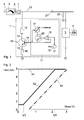
- Figure 1 shows a bleeder circuit 1 connected to a phase-cut dimmer 2 via a rectifier 7.
- the output of the rectifier is also connected to a switched mode power supply 3 which supplies power to a solid state light 4, comprising an LED array.
- the rectifier 7 is connected to the supply 3 via a diode 21 and is also connected to a buffer capacitor 22.
- the buffer capacitor 22 serves to buffer input voltage for the supply 3 such that output current can be delivered continuously, and also during the mains zero crossings and dimmer non-conductive time.
- the diode 21 serves to decouple the output voltage of the rectifier 7 from the buffer voltage across buffer capacitor 22 such that the bleeder circuit 1 can load the dimmer with a current without discharging the buffer capacitor 22.
- diode 21 may not be used and the capacitor 22 may have a lower value.
- the supply 3 will only be active while the dimmer 2 is conducting and sufficient rectified mains voltage is available from rectifier 7. It is appreciated that the power supply 3 may be designed to draw current even for low input voltage when the dimmer is not conducting but this generally leads to uncertainty and variation in the amount of energy supplied to the LED load 4 such that a stable light output cannot be guaranteed.
- the phase-cut dimmer 2 comprises a mains voltage input 5 for receiving an alternating mains voltage supply and a phase-cut output 6 for outputting a phase-cut output signal as per the setting of the dimmer 2.
- the dimmer may comprise a forward edge phase cut dimmer or a backward edge phase cut dimmer.
- the phase-cut signal is rectified by the bridge rectifier 7 and provided to the switched mode power supply 3 and bleeder circuit 1.
- the bleeder circuit 1 is configured to draw a bleed current when required and of an appropriate size for reliable operation of the phase-cut dimmer 2.
- the bleeder circuit 1 includes a bipolar junction transistor (BJT) 10 and a bleeder circuit controller 11.
- the controller 11 may be embodied as an integrated circuit.
- the BJT 10 comprises a collector terminal 12, an emitter terminal 13 and a base terminal 14.
- the controller 11 is connected to the base terminal 14.
- the collector terminal 12 is connected to the output of the bridge rectifier 7.
- a collector resistor 15 is located between the collector terminal 12 and the bridge rectifier 7.
- the resistor 15 is optional and may be provided to distribute thermal dissipation in the circuit 1 by shifting part of the total bleeder circuit dissipation from the BJT 10 to the resistor. In this way, the dissipation is physically distributed, so reducing cost for the thermal design.
- the emitter terminal 13 is configured to be connected to ground via an emitter resistor 16.
- the controller 11 is configured apply a control signal to the base terminal 14 to control the flow of a bleed current through the BJT 10.
- the controller is configured to control the maximum bleed current.
- a voltage source 18 will be controlled to have a different value over time, depending on the type of dimmer detected by the controller (forward or backward phase cut) and the state of the dimmer (conductive state, non-conductive state, on-off transition, off-on transition).
- the bleeder circuit can respond to the operational state of the phase-cut dimmer over each of its cycles to ensure an appropriate bleed current is drawn by the bleed circuit 1 for correct operation of the dimmer 2.
- bleeder circuit 1 operates together with the switched mode power supply 3 to draw this bleed current since the supply 3 cannot draw current from the dimmer 2 when it is in an off-state due to diode 21 and capacitor 22.
- the controller 11 further includes a variable current source 17 that is configured to set a maximum value of the current that can be supplied to the base terminal 14 as a function of the voltage measured at the base terminal 14.
- the voltage source 18 is configured to output the control signal that is used to control the bleed current over the dimmer waveform.
- the voltage source is connected to an error determination element 19.
- the error determination element 19 receives the control signal at one of its terminals and the measured signal indicative of current flow through the dimmer at its other terminal. In this embodiment the voltage at the base 14 provides the measured signal.
- the error determination element 19 controls a MOS transistor 20 by way of a connection to its gate, which in turn controls the current flow between the current source 17 and the base 14.
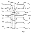
- FIG. 2 shows an example of the voltages and current waveforms for a forward phase cut dimmer.
- V rect is the rectified voltage from the rectifier 7, such as at point 23.
- the waveform is a phase cut sinusoidal mains voltage.
- the voltage is low (typically a few volts) but not exactly zero, as will be appreciated by those skilled in the art.
- I Diode is the current through diode 21 that flows for part of the cycle to charge the buffer capacitor 22.
- I bleed shows an example bleeder current profile that may be used. Such a bleed current profile is achieved by control of the voltage "Vctrl" comprising the output from voltage source 18, as will be described below. Thus, Vctrl comprises the control signal from voltage source 18.
- the BJT 10 will try to draw a high emitter current due to the high control signal voltage setting but the voltage at 23 is low so the BJT 10 has a low collector 12 voltage and it will operate in saturated mode, resulting in a current flow though the bleeder circuit 1 that is determined by the impedance of the dimmer in non-conduction state. Obviously, in this interval, the precise waveform of IBleed depends on the construction of the dimmer. In such a saturated mode, rest of the BJT emitter current is supplied by the base-emitter current which would, in the absence of the current limit, be determined by the output of voltage source 18, Vctrl, and emitter resistor 16 and would be drawn by the base of the BJT 10 and supplied through the transistor 20. The operation of the current limit will be described in more detail below.
- Vctrl is regulated from point 32 onwards to the value required to keep the dimmer conducting.
- the Idiode current is higher than the holding current between 32 and 33, hence Vctrl is lowered to a level such that the bleed current Ibleed is zero.
- the current I diode is lower than the current required to keep the dimmer conducting (known as the holding current).
- the controller 11 is configured to gradually increase the voltage Vctrl of voltage source 18 such that the bleeder current complements the decreasing current through diode 22 to the required level.
- the BJT 10 operates in non-saturated mode.
- the diode current I diode has become zero.
- the control signal Vctrl is therefore constant to provide the holding current and the bleed current IBleed stabilizes to a fixed value.
- the base current can be limited by setting the current source 17 to a fixed maximum value that is high enough to enable the controller to control the BJT to achieve the maximum desired bleeder current (120mA in this example). For example, if the current gain Hfe of the BJT is at least 25, a current limit of about 5mA is appropriate.
- the base current is controlled based on the measured bleeder circuit 1 current, which is indicative of the current through the dimmer 2. This is achieved by measuring the base voltage and setting the current limit according to the function of figure 3 .
- the bleeder circuit current during the non-conduction period may be 10mA. If we assume a worst-case current gain, Hfe, of for example 25, the base current can be limited to 0.4mA. However, it is advantageous to set the maximum current limit higher than this for reliable operation. Thus, in this example, there is current limit margin included and the base current as shown in IB3 can be limited to a peak of 0.5mA during the non-conduction period.
- This control scheme enables the bleeder circuit to transition from pre-30 to post-30 region (off, non-conduction state to conduction-state of dimmer) without requiring a state-change detection or a change of the control voltage (Vctrl).
- the current control function includes a first region in which the current limit increases with the measured variable, which in this example is the voltage at the base, between a first threshold V1 and a second threshold V2.
- the current limit function increases linearly in the first region.
- the control function in this example, has a second region defining a current maximum in which the current limit is held constant above the second threshold V2.
- the current control function may further include a third region in which the current limit is held constant, at an above zero value, while the base voltage is below the first threshold V1.
Landscapes
- Circuit Arrangement For Electric Light Sources In General (AREA)
Abstract
Description
- This invention relates to a bleeder circuit controller for controlling a bipolar junction transistor in a bleeder circuit for use with a phase-cut dimmer. It also relates to a solid state lighting driver including the bleeder circuit controller and a solid state light including the driver and the bleeder circuit controller.
- A phase cut dimmer is used to control the current flow to a load, typically for lighting applications. Phase cut dimmers typically include a triac or other switching device for periodically switching between on (conducting) and off (non-conducting) states at a predetermined phase of the applied waveform wherein the ratio of on-state to off-state provides the current flow control. Phase cut dimmers operate reliably with incandescent bulbs but a bleeder circuit may be required for operation with solid state lighting. In solid state lighting, a switched mode power supply is used to drive an LED array, for example, which has a current draw that may not operate reliably with a phase cut dimmer. In particular, a phase cut dimmer may need a minimum load in order to operate correctly. This can be an issue when connected to an efficient dimmable LED. Further, a "latching current" is required to be drawn to complete the transition from off-state to on-state. For LED lighting, a bleeder circuit may be used to pull the whole or part of this current, termed a "bleed current", required for reliable operation of the phase cut dimmer.
- According to a first aspect of the invention we provide a bleeder circuit controller configured to control a bipolar junction transistor having a collector configured to be connected to a rectified output of a phase cut dimmer to receive a bleed current, an emitter for connecting to ground and a base, the bleeder circuit controller configured to generate a control signal for controlling the bleed current through the bipolar junction transistor and measure a signal indicative of the current flow through the dimmer and apply a current limit to a base-emitter current flow as a function of the measured signal.
- The controller is advantageous as it has been found to reliably control a bipolar junction transistor (BJT) such that it can be used successfully in a bleeder circuit. The use of a BJT in a bleeder circuit is advantageous as they may be more cost effective than MOSFETs used in known bleeder circuits. The determination and application of a current limit as a function of current flow through the dimmer leads to an efficient controller. Thus, the BJT can be controlled such that its current sink capability at the collector adapts to the current through the dimmer to provide an efficient bleed circuit without losing significant drive current into the base of the BJT when it is operating in a saturated mode, for example when the dimmer output voltage is low, such as during the dimmer's non-conduction state. In particular, the BJT may be controlled such that it remains within a linear region of operation or on the edge of saturation and can respond to changes in current flow through the dimmer to adjust the base-emitter current limit through the BJT. Thus, the controller comprises a BJT controller.
- The signal measured by the controller may comprise at least one of;
- a voltage at the base of the bipolar junction transistor;
- a voltage at the emitter of the bipolar junction transistor;
- a voltage at the collector of the bipolar junction transistor; and
- a rectified phase cut mains voltage, the mains voltage comprising the voltage applied to an input of the phase cut dimmer.
- It has been found that each of the above voltages can give the controller an indication of the current flow through the dimmer, which can be used to control the limit on the base-emitter current through BJT while allowing for control of the bleed current. The voltages at the base, emitter and collector may be measured relative to ground.
- The controller may be configured to control the bipolar junction transistor by applying the control signal at the base for controlling the bleed current from the phase-cut dimmer through the bipolar junction transistor. Control of the current at the base can control the flow of the bleed current from the collector to the emitter.
- The controller may include a voltage source and may be configured to control said voltage source to generate said control signal. Thus, the voltage source may be used to control the BJT such that is draws an appropriate bleed current in accordance with a control profile for the particular dimmer and its associated timings.
- The controller may include a current source and may be configured to control the current from the current source as a function of the measured signal. Thus, the output of the current source may be dynamically limited in accordance with the function of the measured signal.
- The controller may include a switch or transistor configured to control the flow of current from the current source to the base of the bipolar junction transistor. The switch may be integrated in an integrated circuit with the controller.
- Alternatively, the base-emitter current may be limited by control of a switch or controllable impedance at the emitter of the BJT. Therefore, the controller may be configured to provide a current limit control signal for controlling the switch connected to the emitter to control the flow of current from the current source to the emitter of the bipolar junction transistor as a function of the measured signal. Thus, rather than controlling the voltage or current to the base of the BJT, one may add a switching element in series between the emitter and ground to control the amount of current flowing from the controller into the base of the BJT. This is advantageous in situations such as when the dimmer current drops by such amount that the BJT would be driven into saturation or in other situations. The switch may comprise a MOS Transistor or a further BJT.
- The controller may generate the control signal such that it controls the BJT to draw a bleed current comprising one or more of;
- an off-state current during an off-state of the phase-cut dimmer;
- a latching current required for a forward phase-cut dimmer to transition between an off-state and an on-state;
- a holding current required for a forward phase cut dimmer to maintain the phase-cut dimmer in an on-state once it is in said on-state;
- a discharge current for a backward phase cut dimmers to lower the dimmer output voltage low at the transition between an on-state and an off-state.
- Thus, the controller may be configured to draw sufficient bleed current as required. A plurality of controllers may be provided for a BJT, each configured to detect when each of the above bleed currents is required and provide a control signal to control the BJT accordingly.
- The controller may include an error determination element such as an error amplifier configured to compare the voltage of the control signal with the measured voltage at the base and control the base-emitter current flow using said comparison. The error determination element may be configured to control the current flow to the base.
- The BJT may be a low voltage device when combined with a cascaded high voltage metal oxide semiconductor transistor (MOST), the collector of the low voltage BJT connected to the source of the high voltage MOST, the drain of the MOST connected to the rectified mains and the gate to a voltage source.
- The base-emitter current flow limit function may comprise a first region in which the current limit increases with the measured signal between a first threshold and a second threshold. The increase may be linear although it could be any other relationship. The function may further include a second region defining a maximum current in which the current limit is held constant when the measured signal exceeds the second threshold. The function may include a third region in which the current limit is held constant, at an above zero value, while the measured signal is below the first threshold. The measured signal may comprise the voltage at the base.
- The function may be configured to limit the base-emitter current such that the controller, when in use, drives the bipolar junction transistor in a linear operation mode substantially on an edge of a saturation mode.
- According to a second aspect of the invention, we provide a bleeder circuit comprising a bipolar junction transistor configured to be controlled by the bleeder circuit controller of the first aspect of the invention.
- The bleeder circuit may include a user settable component, the bleeder circuit controller configured to use said user settable component to determine the maximum allowable current through the bipolar junction transistor.
- The bleeder circuit may include a user replaceable limiting resistor external to the controller and in series with the bipolar junction transistor configured to, in combination with the controller, limit the maximum current through the bipolar junction transistor. The limiting resistor may be located between the emitter and ground.
- The controller may be embodied as an integrated circuit (IC). The limiting resistor may be external to the IC.
- According to a third aspect of the invention we provide a solid state lighting driver including the bleeder circuit of the second aspect of the invention.
- According to a fourth aspect of the invention we provide a solid state light comprising a driver for powering the solid state light, the driver including the bleeder circuit of the second aspect of the invention.
- There now follows, by way of example only, a detailed description of embodiments of the invention with reference to the following figures, in which:
-
Figure 1 shows an embodiment of a bleeder circuit in a solid state lighting application; and -
Figure 2 shows a series of graphs showing waveforms of a rectified output from the phase-cut dimmer, a bleed current profile, the control signal of the controller, the current flow into a driver of a solid state light and three examples of the base-emitter current flow; and -
Figure 3 shows a function of current limit vs. base voltage. -
Figure 1 shows ableeder circuit 1 connected to a phase-cut dimmer 2 via a rectifier 7. The output of the rectifier is also connected to a switchedmode power supply 3 which supplies power to asolid state light 4, comprising an LED array. The rectifier 7 is connected to thesupply 3 via adiode 21 and is also connected to abuffer capacitor 22. Thebuffer capacitor 22 serves to buffer input voltage for thesupply 3 such that output current can be delivered continuously, and also during the mains zero crossings and dimmer non-conductive time. Thediode 21 serves to decouple the output voltage of the rectifier 7 from the buffer voltage acrossbuffer capacitor 22 such that thebleeder circuit 1 can load the dimmer with a current without discharging thebuffer capacitor 22. - In other implementations where a high power factor is desired,
diode 21 may not be used and thecapacitor 22 may have a lower value. In these applications, thesupply 3 will only be active while thedimmer 2 is conducting and sufficient rectified mains voltage is available from rectifier 7. It is appreciated that thepower supply 3 may be designed to draw current even for low input voltage when the dimmer is not conducting but this generally leads to uncertainty and variation in the amount of energy supplied to theLED load 4 such that a stable light output cannot be guaranteed. - The phase-
cut dimmer 2 comprises amains voltage input 5 for receiving an alternating mains voltage supply and a phase-cut output 6 for outputting a phase-cut output signal as per the setting of thedimmer 2. The dimmer may comprise a forward edge phase cut dimmer or a backward edge phase cut dimmer. The phase-cut signal is rectified by the bridge rectifier 7 and provided to the switchedmode power supply 3 andbleeder circuit 1. Thebleeder circuit 1 is configured to draw a bleed current when required and of an appropriate size for reliable operation of the phase-cut dimmer 2. - The
bleeder circuit 1 includes a bipolar junction transistor (BJT) 10 and ableeder circuit controller 11. Thecontroller 11 may be embodied as an integrated circuit. TheBJT 10 comprises acollector terminal 12, anemitter terminal 13 and abase terminal 14. Thecontroller 11 is connected to thebase terminal 14. - The
collector terminal 12 is connected to the output of the bridge rectifier 7. Acollector resistor 15 is located between thecollector terminal 12 and the bridge rectifier 7. Theresistor 15 is optional and may be provided to distribute thermal dissipation in thecircuit 1 by shifting part of the total bleeder circuit dissipation from theBJT 10 to the resistor. In this way, the dissipation is physically distributed, so reducing cost for the thermal design. Theemitter terminal 13 is configured to be connected to ground via anemitter resistor 16. - The
controller 11 is configured apply a control signal to thebase terminal 14 to control the flow of a bleed current through theBJT 10. Thus, the controller is configured to control the maximum bleed current. For this purpose, avoltage source 18 will be controlled to have a different value over time, depending on the type of dimmer detected by the controller (forward or backward phase cut) and the state of the dimmer (conductive state, non-conductive state, on-off transition, off-on transition). Thus, the bleeder circuit can respond to the operational state of the phase-cut dimmer over each of its cycles to ensure an appropriate bleed current is drawn by thebleed circuit 1 for correct operation of thedimmer 2. - In lighting applications requiring compatibility with phase cut dimmers, current has to be drawn by the load during an off state of the dimmer to ensure that the dimmer functions properly. In addition to this off-state current, a certain "latching current" is required to complete a transition from an off-state to an on-state in the dimmer. Thus the
bleeder circuit 1 operates together with the switchedmode power supply 3 to draw this bleed current since thesupply 3 cannot draw current from thedimmer 2 when it is in an off-state due todiode 21 andcapacitor 22. - The
controller 11 further includes a variablecurrent source 17 that is configured to set a maximum value of the current that can be supplied to thebase terminal 14 as a function of the voltage measured at thebase terminal 14. Thevoltage source 18 is configured to output the control signal that is used to control the bleed current over the dimmer waveform. The voltage source is connected to anerror determination element 19. Theerror determination element 19 receives the control signal at one of its terminals and the measured signal indicative of current flow through the dimmer at its other terminal. In this embodiment the voltage at thebase 14 provides the measured signal. Theerror determination element 19 controls aMOS transistor 20 by way of a connection to its gate, which in turn controls the current flow between thecurrent source 17 and thebase 14. - Thus, when the momentary voltage of the rectified mains is high enough to prevent the BJT from saturating (i.e. when the collector voltage is higher than the base voltage), the bleed current will be determined by the output level of the
voltage source 18. A voltage drop across the base-emitter junction may be experienced. The voltage drop (Vbe) may be about 0.7V. The bleed current (Ibleed) may therefore be determined by the control signal and theresistance 16 such that Ibleed=(Vctrl-Vbe)/R16 where R16 is the resistance ofemitter resistor 16. In this mode of operation,error determination element 19, acts as an error amplifier and together withtransistor 20 it functions as a unity gain voltage buffer. - If the collector voltage drops below the base voltage the BJT saturates and the base current increases compared to that in the non-saturated mode of operation. So, without the current limit and if the controller would be capable of supplying an unlimited output current, a high current would flow from the internal IC supply of the controller to the base of the BJT. This is undesired for reason of inefficiency.
- Thus, the controller is configured to limit the maximum current that can be conducted via
transistor 20 into thebase 14 of theBJT 10. The limit on the current is set viacurrent source 17 and is dependent on the measured signal indicative of current flow through the dimmer. In general, the measured signal comprises a measurement of current flow through the bleeder current. Ideally, the current limit is to be set to the value (or just above) of the actual dimmer current divided by the current gain factor (denoted by Hfe) of the BJT. In practice, a margin is taken into account to cover BJTs that have a lower Hfe than average. In this embodiment, as mentioned above, the base voltage is used as the measured signal and an appropriate function is determined. -
Figure 2 shows an example of the voltages and current waveforms for a forward phase cut dimmer. Vrect is the rectified voltage from the rectifier 7, such as atpoint 23. During a dimmer conduction period, the waveform is a phase cut sinusoidal mains voltage. During a dimmer non-conduction period, the voltage is low (typically a few volts) but not exactly zero, as will be appreciated by those skilled in the art. IDiode is the current throughdiode 21 that flows for part of the cycle to charge thebuffer capacitor 22. - Ibleed shows an example bleeder current profile that may be used. Such a bleed current profile is achieved by control of the voltage "Vctrl" comprising the output from
voltage source 18, as will be described below. Thus, Vctrl comprises the control signal fromvoltage source 18. - IB1 is the resulting base current if the base current is solely determined by
voltage source 18 without using the current limit function provided bycurrent source 17. IB2 is the resulting base current if a fixed current limit is used, in this example 5mA. IB3 is the base current when using thecontroller 1 as described in the above embodiment. - Prior to point 30, the
dimmer 2 is in a non-conduction state and the voltage at 23 is low. For an optimal behaviour of the phase cutdimmer 2, thebleeder circuit 1 is required to keep the voltage low. This is achieved by thecontroller 11 setting Vctrl to a predetermined maximum value, which in this example is 3V. Thus, during the non-conduction period, the control signal voltage is set to an upper value. - The
BJT 10 will try to draw a high emitter current due to the high control signal voltage setting but the voltage at 23 is low so theBJT 10 has alow collector 12 voltage and it will operate in saturated mode, resulting in a current flow though thebleeder circuit 1 that is determined by the impedance of the dimmer in non-conduction state. Obviously, in this interval, the precise waveform of IBleed depends on the construction of the dimmer. In such a saturated mode, rest of the BJT emitter current is supplied by the base-emitter current which would, in the absence of the current limit, be determined by the output ofvoltage source 18, Vctrl, andemitter resistor 16 and would be drawn by the base of theBJT 10 and supplied through thetransistor 20. The operation of the current limit will be described in more detail below. - At
point 30, the dimmer starts its conduction phase. It is noted, that as soon as Vrect has stepped to a high value at the start of the conduction period, the base current IB1 drops significantly (by a factor equal to theBJT 10 current gain Hfe) because the operation mode of the BJT10 has changed from saturated to non-saturated. Thebleeder circuit 1 is initially configured to try and keep the voltage at 23 low as this will help the dimmer to latch. When thecontroller 11 has detected that the dimmer has started conducting, i.e atpoint 31, and therefore that the current to thesupply 3 viadiode 22 is high enough to keep the dimmer conducting, thecontroller 11 is configured to ramp down the control signal, Vctrl. - Vctrl is regulated from
point 32 onwards to the value required to keep the dimmer conducting. In this particular example, the Idiode current is higher than the holding current between 32 and 33, hence Vctrl is lowered to a level such that the bleed current Ibleed is zero. - From
point 33 onwards, the current Idiode is lower than the current required to keep the dimmer conducting (known as the holding current). Thecontroller 11 is configured to gradually increase the voltage Vctrl ofvoltage source 18 such that the bleeder current complements the decreasing current throughdiode 22 to the required level. TheBJT 10 operates in non-saturated mode. - At
point 34, the diode current Idiode has become zero. The control signal Vctrl is therefore constant to provide the holding current and the bleed current IBleed stabilizes to a fixed value. - Starting from
point 35, shortly before the mains zero crossing, the controller is configured to set Vctrl high thus placing the bleeder circuit in "high current mode", such that it is prepared to keep thevoltage 23 low during the subsequent non-conduction period starting atpoint 36. - At
point 35, the voltage 6 has dropped to a level where the BJT would again start to operate in saturated mode. As result, the base-emitter current IB1 would typically increase to a high value as shown in graph IB1. This is undesired because the current would come from a controller supply and so reduce power efficiency (regardless of supply arrangement). Thus, limiting the base-emitter current as a function of the base voltage allows the control signal to control the BJT to provide an effective bleeder circuit while limiting the base-emitter current at least when the dimmer is in a non-conduction period. - In a first example, the base current can be limited by setting the
current source 17 to a fixed maximum value that is high enough to enable the controller to control the BJT to achieve the maximum desired bleeder current (120mA in this example). For example, if the current gain Hfe of the BJT is at least 25, a current limit of about 5mA is appropriate. - In a preferred example, the base current is controlled based on the measured
bleeder circuit 1 current, which is indicative of the current through thedimmer 2. This is achieved by measuring the base voltage and setting the current limit according to the function offigure 3 . In this example, the bleeder circuit current during the non-conduction period may be 10mA. If we assume a worst-case current gain, Hfe, of for example 25, the base current can be limited to 0.4mA. However, it is advantageous to set the maximum current limit higher than this for reliable operation. Thus, in this example, there is current limit margin included and the base current as shown in IB3 can be limited to a peak of 0.5mA during the non-conduction period. - This control scheme enables the bleeder circuit to transition from pre-30 to post-30 region (off, non-conduction state to conduction-state of dimmer) without requiring a state-change detection or a change of the control voltage (Vctrl).
- The operational principles described above for a forward phase cut dimmer apply equally to backward phase cut dimmers, with the necessary timing and magnitudes amended accordingly.
-
Figure 3 shows an example of how the current limit set bycurrent source 17 can be controlled depending on the voltage at thebase 14. The dashedline 40 shows the minimum current that needs to be available as function of the base voltage in order to drive the bleed current for aBJT 10 with a current gain, Hfe, of 25 and anemitter resistor 16 of, for example, 18 Ohms, while theBJT 10 is operating in an unsaturated mode. The dottedline 41 is the base current limit set by thecurrent source 17 in the example where a static maximum current value of 5mA is used. Thesolid line 42 shows an example current limit control function. Theline 42 must be above the minimumcurrent line 40 but for optimal efficiency, the currentlimit control function 42 should still be relatively close to the requiredminimum 40. Thus the current control function includes a first region in which the current limit increases with the measured variable, which in this example is the voltage at the base, between a first threshold V1 and a second threshold V2. In this example, the current limit function increases linearly in the first region. The control function, in this example, has a second region defining a current maximum in which the current limit is held constant above the second threshold V2. The current control function may further include a third region in which the current limit is held constant, at an above zero value, while the base voltage is below the first threshold V1.
Claims (15)
- A bleeder circuit controller configured to control a bipolar junction transistor having a collector configured to be connected to a rectified output of a phase cut dimmer to receive a bleed current, an emitter for connecting to ground and a base, the bleeder circuit controller configured to generate a control signal for controlling the bleed current through the bipolar junction transistor and measure a signal indicative of the current flow through the dimmer and apply a current limit to a base-emitter current flow as a function of the measured signal.
- A bleeder circuit controller as defined in claim 1, in which the signal indicative of the current flow through the dimmer comprises at least one of;
a voltage at the base of the bipolar junction transistor;
a voltage at the emitter of the bipolar junction transistor;
a voltage at the collector of the bipolar junction transistor; and
a rectified, phase cut mains voltage, the mains voltage comprising the voltage applied to an input of the phase cut dimmer. - A bleeder circuit controller as defined in claim 1 or claim 2, in which the controller is configured to control the bipolar junction transistor by applying the control signal at the base for controlling the bleed current from the phase-cut dimmer through the bipolar junction transistor.
- A bleeder circuit controller as defined in claim 3, in which the controller includes a voltage source and is configured to control said voltage source to generate said control signal.
- A bleeder circuit controller as defined in claim 3 or claim 4, in which the controller is configured to control the current of the control signal as a function of the measured signal to provide said current limit.
- A bleeder circuit controller as defined in claim 5, in which the controller includes a transistor configured to control the flow of current to the base of the bipolar junction transistor.
- A bleeder circuit controller as defined in claim 5, in which the controller is configured to provide a current limit control signal for controlling a controllable impedance connected to the emitter to control the flow of current from the controller to the base of the bipolar junction transistor.
- A bleeder circuit controller as defined in any preceding claim, in which the control signal generated by the controller is configured to control the bleed current to provide;
an off-state current during an off-state of the phase-cut dimmer;
a latching current required for the phase-cut dimmer to transition between an off-state and an on-state;
a holding current required to maintain the phase-cut dimmer in an on-state once it is in said on-state.
a discharge current for backward phase cut dimmers to pull the dimmer output voltage low at the transition between an on-state and an off-state. - A bleeder circuit controller as defined in any preceding claim, in which the controller includes an error determination element configured to compare the voltage of the control signal with the measured voltage at the base and control the base-emitter current flow using said comparison.
- A bleeder circuit controller as defined in any preceding claim, in which the function comprises a first region in which the base-emitter current limit increases with the measured signal between a first threshold and a second threshold.
- A bleeder circuit controller as defined in claim 10, in which the function further includes a second region defining a maximum current in which the current limit is held constant when the measured signal exceeds the second threshold.
- A bleeder circuit controller as defined in any preceding claim, in which the function is configured to limit the base-emitter current such that the controller, when in use, drives the bipolar junction transistor in a linear operation mode substantially on an edge of a saturation mode.
- A bleeder circuit comprising a bipolar junction transistor configured to be controlled by the bleeder circuit controller of any one of claims 1 to 12.
- A bleeder circuit as defined in claim 13, the bipolar junction transistor arranged to be cascaded with a metal oxide semiconductor transistor (MOST), the collector of the bipolar junction transistor connected to a source of MOST, the drain of the MOST connected to a rectified mains signal and the gate to a fixed voltage source.
- A solid state light comprising a driver for powering the solid state light, the driver including the bleeder circuit of claim 13 or 14.
Priority Applications (3)
| Application Number | Priority Date | Filing Date | Title |
|---|---|---|---|
| EP13199557.3A EP2890220B1 (en) | 2013-12-24 | 2013-12-24 | Bleeder circuit controller |
| CN201410696623.7A CN104735860B (en) | 2013-12-24 | 2014-11-26 | Leadage circuit controller |
| US14/564,659 US9532416B2 (en) | 2013-12-24 | 2014-12-09 | Bleeder circuit controller |
Applications Claiming Priority (1)
| Application Number | Priority Date | Filing Date | Title |
|---|---|---|---|
| EP13199557.3A EP2890220B1 (en) | 2013-12-24 | 2013-12-24 | Bleeder circuit controller |
Publications (2)
| Publication Number | Publication Date |
|---|---|
| EP2890220A1 true EP2890220A1 (en) | 2015-07-01 |
| EP2890220B1 EP2890220B1 (en) | 2023-10-25 |
Family
ID=49943141
Family Applications (1)
| Application Number | Title | Priority Date | Filing Date |
|---|---|---|---|
| EP13199557.3A Active EP2890220B1 (en) | 2013-12-24 | 2013-12-24 | Bleeder circuit controller |
Country Status (3)
| Country | Link |
|---|---|
| US (1) | US9532416B2 (en) |
| EP (1) | EP2890220B1 (en) |
| CN (1) | CN104735860B (en) |
Families Citing this family (5)
| Publication number | Priority date | Publication date | Assignee | Title |
|---|---|---|---|---|
| KR102453820B1 (en) | 2015-08-21 | 2022-10-17 | 서울반도체 주식회사 | Driving circuit and lighting apparatus for light emitting diode |
| CN106879125B (en) * | 2017-04-13 | 2018-07-10 | 上海新进半导体制造有限公司 | A kind of LED adjusting control circuits |
| CN108366460B (en) * | 2018-04-11 | 2019-11-05 | 矽力杰半导体技术(杭州)有限公司 | Leadage circuit and LED drive circuit |
| CN113325395B (en) * | 2020-02-28 | 2024-08-27 | 华为技术有限公司 | A laser receiving circuit, a laser radar and a vehicle |
| CN111432526B (en) | 2020-04-13 | 2023-02-21 | 昂宝电子(上海)有限公司 | Control system and method for power factor optimization of LED lighting systems |
Citations (3)
| Publication number | Priority date | Publication date | Assignee | Title |
|---|---|---|---|---|
| WO2011013060A2 (en) * | 2009-07-27 | 2011-02-03 | Koninklijke Philips Electronics N.V. | Bleeder circuit |
| EP2373124A1 (en) * | 2010-04-01 | 2011-10-05 | Rohm Co., Ltd. | Driver circuit for driving a lighting device and method for operating the same |
| EP2608636A1 (en) * | 2011-12-19 | 2013-06-26 | Nxp B.V. | Method and apparatus for management of power supplied from a phase-cut ac supply |
Family Cites Families (10)
| Publication number | Priority date | Publication date | Assignee | Title |
|---|---|---|---|---|
| US5416387A (en) * | 1993-11-24 | 1995-05-16 | California Institute Of Technology | Single stage, high power factor, gas discharge lamp ballast |
| GB2435724A (en) * | 2006-03-04 | 2007-09-05 | Mood Concepts Ltd | TRIAC dimming of LED lighting units |
| CN101080118A (en) * | 2006-05-22 | 2007-11-28 | 陈建中 | Current control device for light-emitting diode modules |
| US8212494B2 (en) * | 2008-04-04 | 2012-07-03 | Lemnis Lighting Patents Holding B.V. | Dimmer triggering circuit, dimmer system and dimmable device |
| CN102548095B (en) * | 2010-12-22 | 2014-01-08 | 海洋王照明科技股份有限公司 | Lamp and driving circuit thereof |
| KR20120080908A (en) * | 2011-01-10 | 2012-07-18 | 페어차일드코리아반도체 주식회사 | Apparatus for controlling bleed switch, power supply, and method for driving power supply |
| EP2590477B1 (en) * | 2011-11-07 | 2018-04-25 | Silergy Corp. | A method of controlling a ballast, a ballast, a lighting controller, and a digital signal processor |
| EP2608637B1 (en) * | 2011-12-21 | 2018-11-14 | Silergy Corp. | Leading-edge phase-cut bleeder control |
| TWI481310B (en) * | 2012-08-10 | 2015-04-11 | Unity Opto Technology Co Ltd | Light emitting diode drive |
| EP2887767B1 (en) | 2013-12-17 | 2018-02-14 | Silergy Corp. | Switching power supply controller |
-
2013
- 2013-12-24 EP EP13199557.3A patent/EP2890220B1/en active Active
-
2014
- 2014-11-26 CN CN201410696623.7A patent/CN104735860B/en active Active
- 2014-12-09 US US14/564,659 patent/US9532416B2/en active Active
Patent Citations (3)
| Publication number | Priority date | Publication date | Assignee | Title |
|---|---|---|---|---|
| WO2011013060A2 (en) * | 2009-07-27 | 2011-02-03 | Koninklijke Philips Electronics N.V. | Bleeder circuit |
| EP2373124A1 (en) * | 2010-04-01 | 2011-10-05 | Rohm Co., Ltd. | Driver circuit for driving a lighting device and method for operating the same |
| EP2608636A1 (en) * | 2011-12-19 | 2013-06-26 | Nxp B.V. | Method and apparatus for management of power supplied from a phase-cut ac supply |
Also Published As
| Publication number | Publication date |
|---|---|
| US20150181669A1 (en) | 2015-06-25 |
| CN104735860A (en) | 2015-06-24 |
| EP2890220B1 (en) | 2023-10-25 |
| CN104735860B (en) | 2017-12-22 |
| US9532416B2 (en) | 2016-12-27 |
Similar Documents
| Publication | Publication Date | Title |
|---|---|---|
| US11856670B2 (en) | Systems and methods for providing power supply to current controllers associated with LED lighting | |
| CN111727566B (en) | Electronic switches and dimmers | |
| US8212494B2 (en) | Dimmer triggering circuit, dimmer system and dimmable device | |
| US9307593B1 (en) | Dynamic bleeder current control for LED dimmers | |
| US9124171B2 (en) | Adaptive current limiter and dimmer system including the same | |
| EP3026988A1 (en) | Power converter controller with analog controlled variable current circuit | |
| TWI511605B (en) | Dynamic control of power switching bipolar junction transistor | |
| CN103945619B (en) | Dimmable LED drive circuit | |
| EP2745368B1 (en) | Start-up circuit | |
| US9532416B2 (en) | Bleeder circuit controller | |
| TW201215224A (en) | Open LED control circuit and associated method | |
| EP3644691A1 (en) | Bleeder circuit and led driving circuit applying the same | |
| EP2974540B1 (en) | Reduction of supply current variations using compensation current control | |
| EP2373124A1 (en) | Driver circuit for driving a lighting device and method for operating the same | |
| JP2004505593A (en) | Interface circuit and method | |
| US10237932B1 (en) | Light-emitting diode lighting system with automatic bleeder current control | |
| US10334682B1 (en) | Light-emitting diode lighting system with automatic bleeder current control | |
| CN110913529B (en) | LED lighting system with automatic bleeder current control | |
| US11224103B2 (en) | LED lighting apparatus | |
| JP2016062686A (en) | LED lighting device | |
| CN204986459U (en) | Light emitting diode lamp | |
| US20140021872A1 (en) | Circuit for controlling a lighting unit with light-emitting diodes | |
| JP2019207833A (en) | Power supply device for illumination | |
| CN203086784U (en) | LED driving circuit and LED illuminating device | |
| US10299325B2 (en) | Optoelectronic circuit with light-emitting diodes |
Legal Events
| Date | Code | Title | Description |
|---|---|---|---|
| PUAI | Public reference made under article 153(3) epc to a published international application that has entered the european phase |
Free format text: ORIGINAL CODE: 0009012 |
|
| 17P | Request for examination filed |
Effective date: 20140327 |
|
| AK | Designated contracting states |
Kind code of ref document: A1 Designated state(s): AL AT BE BG CH CY CZ DE DK EE ES FI FR GB GR HR HU IE IS IT LI LT LU LV MC MK MT NL NO PL PT RO RS SE SI SK SM TR |
|
| AX | Request for extension of the european patent |
Extension state: BA ME |
|
| RBV | Designated contracting states (corrected) |
Designated state(s): AL AT BE BG CH CY CZ DE DK EE ES FI FR GB GR HR HU IE IS IT LI LT LU LV MC MK MT NL NO PL PT RO RS SE SI SK SM TR |
|
| RAP1 | Party data changed (applicant data changed or rights of an application transferred) |
Owner name: SILERGY CORP. |
|
| STAA | Information on the status of an ep patent application or granted ep patent |
Free format text: STATUS: EXAMINATION IS IN PROGRESS |
|
| 17Q | First examination report despatched |
Effective date: 20200124 |
|
| RAP1 | Party data changed (applicant data changed or rights of an application transferred) |
Owner name: SILERGY SEMICONDUCTOR (HONG KONG) LIMITED |
|
| REG | Reference to a national code |
Ref country code: DE Ref legal event code: R079 Free format text: PREVIOUS MAIN CLASS: H05B0033080000 Ipc: H05B0045100000 Ref country code: DE Ref legal event code: R079 Ref document number: 602013084842 Country of ref document: DE Free format text: PREVIOUS MAIN CLASS: H05B0033080000 Ipc: H05B0045100000 |
|
| GRAP | Despatch of communication of intention to grant a patent |
Free format text: ORIGINAL CODE: EPIDOSNIGR1 |
|
| STAA | Information on the status of an ep patent application or granted ep patent |
Free format text: STATUS: GRANT OF PATENT IS INTENDED |
|
| RIC1 | Information provided on ipc code assigned before grant |
Ipc: H05B 45/3725 20200101ALI20230704BHEP Ipc: H05B 45/3575 20200101ALI20230704BHEP Ipc: H05B 45/10 20200101AFI20230704BHEP |
|
| INTG | Intention to grant announced |
Effective date: 20230720 |
|
| GRAS | Grant fee paid |
Free format text: ORIGINAL CODE: EPIDOSNIGR3 |
|
| GRAA | (expected) grant |
Free format text: ORIGINAL CODE: 0009210 |
|
| STAA | Information on the status of an ep patent application or granted ep patent |
Free format text: STATUS: THE PATENT HAS BEEN GRANTED |
|
| AK | Designated contracting states |
Kind code of ref document: B1 Designated state(s): AL AT BE BG CH CY CZ DE DK EE ES FI FR GB GR HR HU IE IS IT LI LT LU LV MC MK MT NL NO PL PT RO RS SE SI SK SM TR |
|
| REG | Reference to a national code |
Ref country code: GB Ref legal event code: FG4D |
|
| REG | Reference to a national code |
Ref country code: CH Ref legal event code: EP |
|
| REG | Reference to a national code |
Ref country code: DE Ref legal event code: R096 Ref document number: 602013084842 Country of ref document: DE |
|
| REG | Reference to a national code |
Ref country code: IE Ref legal event code: FG4D |
|
| REG | Reference to a national code |
Ref country code: LT Ref legal event code: MG9D |
|
| REG | Reference to a national code |
Ref country code: NL Ref legal event code: MP Effective date: 20231025 |
|
| REG | Reference to a national code |
Ref country code: AT Ref legal event code: MK05 Ref document number: 1626049 Country of ref document: AT Kind code of ref document: T Effective date: 20231025 |
|
| PG25 | Lapsed in a contracting state [announced via postgrant information from national office to epo] |
Ref country code: NL Free format text: LAPSE BECAUSE OF FAILURE TO SUBMIT A TRANSLATION OF THE DESCRIPTION OR TO PAY THE FEE WITHIN THE PRESCRIBED TIME-LIMIT Effective date: 20231025 |
|
| PG25 | Lapsed in a contracting state [announced via postgrant information from national office to epo] |
Ref country code: GR Free format text: LAPSE BECAUSE OF FAILURE TO SUBMIT A TRANSLATION OF THE DESCRIPTION OR TO PAY THE FEE WITHIN THE PRESCRIBED TIME-LIMIT Effective date: 20240126 |
|
| PG25 | Lapsed in a contracting state [announced via postgrant information from national office to epo] |
Ref country code: IS Free format text: LAPSE BECAUSE OF FAILURE TO SUBMIT A TRANSLATION OF THE DESCRIPTION OR TO PAY THE FEE WITHIN THE PRESCRIBED TIME-LIMIT Effective date: 20240225 |
|
| PG25 | Lapsed in a contracting state [announced via postgrant information from national office to epo] |
Ref country code: LT Free format text: LAPSE BECAUSE OF FAILURE TO SUBMIT A TRANSLATION OF THE DESCRIPTION OR TO PAY THE FEE WITHIN THE PRESCRIBED TIME-LIMIT Effective date: 20231025 |
|
| PG25 | Lapsed in a contracting state [announced via postgrant information from national office to epo] |
Ref country code: AT Free format text: LAPSE BECAUSE OF FAILURE TO SUBMIT A TRANSLATION OF THE DESCRIPTION OR TO PAY THE FEE WITHIN THE PRESCRIBED TIME-LIMIT Effective date: 20231025 |
|
| PG25 | Lapsed in a contracting state [announced via postgrant information from national office to epo] |
Ref country code: ES Free format text: LAPSE BECAUSE OF FAILURE TO SUBMIT A TRANSLATION OF THE DESCRIPTION OR TO PAY THE FEE WITHIN THE PRESCRIBED TIME-LIMIT Effective date: 20231025 |
|
| PG25 | Lapsed in a contracting state [announced via postgrant information from national office to epo] |
Ref country code: LT Free format text: LAPSE BECAUSE OF FAILURE TO SUBMIT A TRANSLATION OF THE DESCRIPTION OR TO PAY THE FEE WITHIN THE PRESCRIBED TIME-LIMIT Effective date: 20231025 Ref country code: IS Free format text: LAPSE BECAUSE OF FAILURE TO SUBMIT A TRANSLATION OF THE DESCRIPTION OR TO PAY THE FEE WITHIN THE PRESCRIBED TIME-LIMIT Effective date: 20240225 Ref country code: GR Free format text: LAPSE BECAUSE OF FAILURE TO SUBMIT A TRANSLATION OF THE DESCRIPTION OR TO PAY THE FEE WITHIN THE PRESCRIBED TIME-LIMIT Effective date: 20240126 Ref country code: ES Free format text: LAPSE BECAUSE OF FAILURE TO SUBMIT A TRANSLATION OF THE DESCRIPTION OR TO PAY THE FEE WITHIN THE PRESCRIBED TIME-LIMIT Effective date: 20231025 Ref country code: BG Free format text: LAPSE BECAUSE OF FAILURE TO SUBMIT A TRANSLATION OF THE DESCRIPTION OR TO PAY THE FEE WITHIN THE PRESCRIBED TIME-LIMIT Effective date: 20240125 Ref country code: AT Free format text: LAPSE BECAUSE OF FAILURE TO SUBMIT A TRANSLATION OF THE DESCRIPTION OR TO PAY THE FEE WITHIN THE PRESCRIBED TIME-LIMIT Effective date: 20231025 Ref country code: PT Free format text: LAPSE BECAUSE OF FAILURE TO SUBMIT A TRANSLATION OF THE DESCRIPTION OR TO PAY THE FEE WITHIN THE PRESCRIBED TIME-LIMIT Effective date: 20240226 |
|
| PG25 | Lapsed in a contracting state [announced via postgrant information from national office to epo] |
Ref country code: SE Free format text: LAPSE BECAUSE OF FAILURE TO SUBMIT A TRANSLATION OF THE DESCRIPTION OR TO PAY THE FEE WITHIN THE PRESCRIBED TIME-LIMIT Effective date: 20231025 Ref country code: RS Free format text: LAPSE BECAUSE OF FAILURE TO SUBMIT A TRANSLATION OF THE DESCRIPTION OR TO PAY THE FEE WITHIN THE PRESCRIBED TIME-LIMIT Effective date: 20231025 Ref country code: PL Free format text: LAPSE BECAUSE OF FAILURE TO SUBMIT A TRANSLATION OF THE DESCRIPTION OR TO PAY THE FEE WITHIN THE PRESCRIBED TIME-LIMIT Effective date: 20231025 Ref country code: NO Free format text: LAPSE BECAUSE OF FAILURE TO SUBMIT A TRANSLATION OF THE DESCRIPTION OR TO PAY THE FEE WITHIN THE PRESCRIBED TIME-LIMIT Effective date: 20240125 Ref country code: LV Free format text: LAPSE BECAUSE OF FAILURE TO SUBMIT A TRANSLATION OF THE DESCRIPTION OR TO PAY THE FEE WITHIN THE PRESCRIBED TIME-LIMIT Effective date: 20231025 Ref country code: HR Free format text: LAPSE BECAUSE OF FAILURE TO SUBMIT A TRANSLATION OF THE DESCRIPTION OR TO PAY THE FEE WITHIN THE PRESCRIBED TIME-LIMIT Effective date: 20231025 |
|
| PG25 | Lapsed in a contracting state [announced via postgrant information from national office to epo] |
Ref country code: DK Free format text: LAPSE BECAUSE OF FAILURE TO SUBMIT A TRANSLATION OF THE DESCRIPTION OR TO PAY THE FEE WITHIN THE PRESCRIBED TIME-LIMIT Effective date: 20231025 |
|
| PG25 | Lapsed in a contracting state [announced via postgrant information from national office to epo] |
Ref country code: CZ Free format text: LAPSE BECAUSE OF FAILURE TO SUBMIT A TRANSLATION OF THE DESCRIPTION OR TO PAY THE FEE WITHIN THE PRESCRIBED TIME-LIMIT Effective date: 20231025 |
|
| REG | Reference to a national code |
Ref country code: DE Ref legal event code: R097 Ref document number: 602013084842 Country of ref document: DE |
|
| PG25 | Lapsed in a contracting state [announced via postgrant information from national office to epo] |
Ref country code: SK Free format text: LAPSE BECAUSE OF FAILURE TO SUBMIT A TRANSLATION OF THE DESCRIPTION OR TO PAY THE FEE WITHIN THE PRESCRIBED TIME-LIMIT Effective date: 20231025 |
|
| PG25 | Lapsed in a contracting state [announced via postgrant information from national office to epo] |
Ref country code: SM Free format text: LAPSE BECAUSE OF FAILURE TO SUBMIT A TRANSLATION OF THE DESCRIPTION OR TO PAY THE FEE WITHIN THE PRESCRIBED TIME-LIMIT Effective date: 20231025 Ref country code: SK Free format text: LAPSE BECAUSE OF FAILURE TO SUBMIT A TRANSLATION OF THE DESCRIPTION OR TO PAY THE FEE WITHIN THE PRESCRIBED TIME-LIMIT Effective date: 20231025 Ref country code: RO Free format text: LAPSE BECAUSE OF FAILURE TO SUBMIT A TRANSLATION OF THE DESCRIPTION OR TO PAY THE FEE WITHIN THE PRESCRIBED TIME-LIMIT Effective date: 20231025 Ref country code: IT Free format text: LAPSE BECAUSE OF FAILURE TO SUBMIT A TRANSLATION OF THE DESCRIPTION OR TO PAY THE FEE WITHIN THE PRESCRIBED TIME-LIMIT Effective date: 20231025 Ref country code: EE Free format text: LAPSE BECAUSE OF FAILURE TO SUBMIT A TRANSLATION OF THE DESCRIPTION OR TO PAY THE FEE WITHIN THE PRESCRIBED TIME-LIMIT Effective date: 20231025 Ref country code: DK Free format text: LAPSE BECAUSE OF FAILURE TO SUBMIT A TRANSLATION OF THE DESCRIPTION OR TO PAY THE FEE WITHIN THE PRESCRIBED TIME-LIMIT Effective date: 20231025 Ref country code: CZ Free format text: LAPSE BECAUSE OF FAILURE TO SUBMIT A TRANSLATION OF THE DESCRIPTION OR TO PAY THE FEE WITHIN THE PRESCRIBED TIME-LIMIT Effective date: 20231025 |
|
| REG | Reference to a national code |
Ref country code: CH Ref legal event code: PL |
|
| PG25 | Lapsed in a contracting state [announced via postgrant information from national office to epo] |
Ref country code: LU Free format text: LAPSE BECAUSE OF NON-PAYMENT OF DUE FEES Effective date: 20231224 |
|
| PG25 | Lapsed in a contracting state [announced via postgrant information from national office to epo] |
Ref country code: MC Free format text: LAPSE BECAUSE OF FAILURE TO SUBMIT A TRANSLATION OF THE DESCRIPTION OR TO PAY THE FEE WITHIN THE PRESCRIBED TIME-LIMIT Effective date: 20231025 |
|
| REG | Reference to a national code |
Ref country code: BE Ref legal event code: MM Effective date: 20231231 |
|
| PG25 | Lapsed in a contracting state [announced via postgrant information from national office to epo] |
Ref country code: MC Free format text: LAPSE BECAUSE OF FAILURE TO SUBMIT A TRANSLATION OF THE DESCRIPTION OR TO PAY THE FEE WITHIN THE PRESCRIBED TIME-LIMIT Effective date: 20231025 Ref country code: LU Free format text: LAPSE BECAUSE OF NON-PAYMENT OF DUE FEES Effective date: 20231224 |
|
| PLBE | No opposition filed within time limit |
Free format text: ORIGINAL CODE: 0009261 |
|
| STAA | Information on the status of an ep patent application or granted ep patent |
Free format text: STATUS: NO OPPOSITION FILED WITHIN TIME LIMIT |
|
| 26N | No opposition filed |
Effective date: 20240726 |
|
| REG | Reference to a national code |
Ref country code: IE Ref legal event code: MM4A |
|
| PG25 | Lapsed in a contracting state [announced via postgrant information from national office to epo] |
Ref country code: IE Free format text: LAPSE BECAUSE OF NON-PAYMENT OF DUE FEES Effective date: 20231224 |
|
| PG25 | Lapsed in a contracting state [announced via postgrant information from national office to epo] |
Ref country code: BE Free format text: LAPSE BECAUSE OF NON-PAYMENT OF DUE FEES Effective date: 20231231 |
|
| PG25 | Lapsed in a contracting state [announced via postgrant information from national office to epo] |
Ref country code: CH Free format text: LAPSE BECAUSE OF NON-PAYMENT OF DUE FEES Effective date: 20231231 |
|
| PG25 | Lapsed in a contracting state [announced via postgrant information from national office to epo] |
Ref country code: SI Free format text: LAPSE BECAUSE OF FAILURE TO SUBMIT A TRANSLATION OF THE DESCRIPTION OR TO PAY THE FEE WITHIN THE PRESCRIBED TIME-LIMIT Effective date: 20231025 |
|
| PG25 | Lapsed in a contracting state [announced via postgrant information from national office to epo] |
Ref country code: SI Free format text: LAPSE BECAUSE OF FAILURE TO SUBMIT A TRANSLATION OF THE DESCRIPTION OR TO PAY THE FEE WITHIN THE PRESCRIBED TIME-LIMIT Effective date: 20231025 Ref country code: IE Free format text: LAPSE BECAUSE OF NON-PAYMENT OF DUE FEES Effective date: 20231224 Ref country code: CH Free format text: LAPSE BECAUSE OF NON-PAYMENT OF DUE FEES Effective date: 20231231 Ref country code: BE Free format text: LAPSE BECAUSE OF NON-PAYMENT OF DUE FEES Effective date: 20231231 |
|
| PG25 | Lapsed in a contracting state [announced via postgrant information from national office to epo] |
Ref country code: FI Free format text: LAPSE BECAUSE OF FAILURE TO SUBMIT A TRANSLATION OF THE DESCRIPTION OR TO PAY THE FEE WITHIN THE PRESCRIBED TIME-LIMIT Effective date: 20231025 |
|
| PG25 | Lapsed in a contracting state [announced via postgrant information from national office to epo] |
Ref country code: CY Free format text: LAPSE BECAUSE OF FAILURE TO SUBMIT A TRANSLATION OF THE DESCRIPTION OR TO PAY THE FEE WITHIN THE PRESCRIBED TIME-LIMIT; INVALID AB INITIO Effective date: 20131224 |
|
| PG25 | Lapsed in a contracting state [announced via postgrant information from national office to epo] |
Ref country code: HU Free format text: LAPSE BECAUSE OF FAILURE TO SUBMIT A TRANSLATION OF THE DESCRIPTION OR TO PAY THE FEE WITHIN THE PRESCRIBED TIME-LIMIT; INVALID AB INITIO Effective date: 20131224 |
|
| PG25 | Lapsed in a contracting state [announced via postgrant information from national office to epo] |
Ref country code: TR Free format text: LAPSE BECAUSE OF FAILURE TO SUBMIT A TRANSLATION OF THE DESCRIPTION OR TO PAY THE FEE WITHIN THE PRESCRIBED TIME-LIMIT Effective date: 20231025 |
|
| PGFP | Annual fee paid to national office [announced via postgrant information from national office to epo] |
Ref country code: GB Payment date: 20251229 Year of fee payment: 13 |
|
| PGFP | Annual fee paid to national office [announced via postgrant information from national office to epo] |
Ref country code: FR Payment date: 20251230 Year of fee payment: 13 |
|
| PGFP | Annual fee paid to national office [announced via postgrant information from national office to epo] |
Ref country code: DE Payment date: 20251231 Year of fee payment: 13 |