EP2887396A1 - Three-dimensional resistive memory array - Google Patents
Three-dimensional resistive memory array Download PDFInfo
- Publication number
- EP2887396A1 EP2887396A1 EP14150456.3A EP14150456A EP2887396A1 EP 2887396 A1 EP2887396 A1 EP 2887396A1 EP 14150456 A EP14150456 A EP 14150456A EP 2887396 A1 EP2887396 A1 EP 2887396A1
- Authority
- EP
- European Patent Office
- Prior art keywords
- type
- layer
- stack
- trenches
- memory array
- Prior art date
- Legal status (The legal status is an assumption and is not a legal conclusion. Google has not performed a legal analysis and makes no representation as to the accuracy of the status listed.)
- Granted
Links
Images





Classifications
-
- H—ELECTRICITY
- H10—SEMICONDUCTOR DEVICES; ELECTRIC SOLID-STATE DEVICES NOT OTHERWISE PROVIDED FOR
- H10B—ELECTRONIC MEMORY DEVICES
- H10B53/00—Ferroelectric RAM [FeRAM] devices comprising ferroelectric memory capacitors
- H10B53/20—Ferroelectric RAM [FeRAM] devices comprising ferroelectric memory capacitors characterised by the three-dimensional [3D] arrangements, e.g. with cells on different height levels
-
- H—ELECTRICITY
- H10—SEMICONDUCTOR DEVICES; ELECTRIC SOLID-STATE DEVICES NOT OTHERWISE PROVIDED FOR
- H10B—ELECTRONIC MEMORY DEVICES
- H10B63/00—Resistance change memory devices, e.g. resistive RAM [ReRAM] devices
- H10B63/30—Resistance change memory devices, e.g. resistive RAM [ReRAM] devices comprising selection components having three or more electrodes, e.g. transistors
-
- H—ELECTRICITY
- H10—SEMICONDUCTOR DEVICES; ELECTRIC SOLID-STATE DEVICES NOT OTHERWISE PROVIDED FOR
- H10B—ELECTRONIC MEMORY DEVICES
- H10B63/00—Resistance change memory devices, e.g. resistive RAM [ReRAM] devices
- H10B63/80—Arrangements comprising multiple bistable or multi-stable switching components of the same type on a plane parallel to the substrate, e.g. cross-point arrays
- H10B63/84—Arrangements comprising multiple bistable or multi-stable switching components of the same type on a plane parallel to the substrate, e.g. cross-point arrays arranged in a direction perpendicular to the substrate, e.g. 3D cell arrays
-
- H—ELECTRICITY
- H10—SEMICONDUCTOR DEVICES; ELECTRIC SOLID-STATE DEVICES NOT OTHERWISE PROVIDED FOR
- H10B—ELECTRONIC MEMORY DEVICES
- H10B63/00—Resistance change memory devices, e.g. resistive RAM [ReRAM] devices
- H10B63/80—Arrangements comprising multiple bistable or multi-stable switching components of the same type on a plane parallel to the substrate, e.g. cross-point arrays
- H10B63/84—Arrangements comprising multiple bistable or multi-stable switching components of the same type on a plane parallel to the substrate, e.g. cross-point arrays arranged in a direction perpendicular to the substrate, e.g. 3D cell arrays
- H10B63/845—Arrangements comprising multiple bistable or multi-stable switching components of the same type on a plane parallel to the substrate, e.g. cross-point arrays arranged in a direction perpendicular to the substrate, e.g. 3D cell arrays the switching components being connected to a common vertical conductor
-
- H—ELECTRICITY
- H10—SEMICONDUCTOR DEVICES; ELECTRIC SOLID-STATE DEVICES NOT OTHERWISE PROVIDED FOR
- H10N—ELECTRIC SOLID-STATE DEVICES NOT OTHERWISE PROVIDED FOR
- H10N70/00—Solid-state devices having no potential barriers, and specially adapted for rectifying, amplifying, oscillating or switching
- H10N70/011—Manufacture or treatment of multistable switching devices
- H10N70/021—Formation of switching materials, e.g. deposition of layers
-
- H—ELECTRICITY
- H10—SEMICONDUCTOR DEVICES; ELECTRIC SOLID-STATE DEVICES NOT OTHERWISE PROVIDED FOR
- H10N—ELECTRIC SOLID-STATE DEVICES NOT OTHERWISE PROVIDED FOR
- H10N70/00—Solid-state devices having no potential barriers, and specially adapted for rectifying, amplifying, oscillating or switching
- H10N70/011—Manufacture or treatment of multistable switching devices
- H10N70/061—Shaping switching materials
- H10N70/063—Shaping switching materials by etching of pre-deposited switching material layers, e.g. lithography
-
- H—ELECTRICITY
- H10—SEMICONDUCTOR DEVICES; ELECTRIC SOLID-STATE DEVICES NOT OTHERWISE PROVIDED FOR
- H10N—ELECTRIC SOLID-STATE DEVICES NOT OTHERWISE PROVIDED FOR
- H10N70/00—Solid-state devices having no potential barriers, and specially adapted for rectifying, amplifying, oscillating or switching
- H10N70/011—Manufacture or treatment of multistable switching devices
- H10N70/061—Shaping switching materials
- H10N70/066—Shaping switching materials by filling of openings, e.g. damascene method
-
- H—ELECTRICITY
- H10—SEMICONDUCTOR DEVICES; ELECTRIC SOLID-STATE DEVICES NOT OTHERWISE PROVIDED FOR
- H10N—ELECTRIC SOLID-STATE DEVICES NOT OTHERWISE PROVIDED FOR
- H10N70/00—Solid-state devices having no potential barriers, and specially adapted for rectifying, amplifying, oscillating or switching
- H10N70/801—Constructional details of multistable switching devices
- H10N70/821—Device geometry
- H10N70/826—Device geometry adapted for essentially vertical current flow, e.g. sandwich or pillar type devices
-
- H—ELECTRICITY
- H10—SEMICONDUCTOR DEVICES; ELECTRIC SOLID-STATE DEVICES NOT OTHERWISE PROVIDED FOR
- H10N—ELECTRIC SOLID-STATE DEVICES NOT OTHERWISE PROVIDED FOR
- H10N70/00—Solid-state devices having no potential barriers, and specially adapted for rectifying, amplifying, oscillating or switching
- H10N70/801—Constructional details of multistable switching devices
- H10N70/881—Switching materials
- H10N70/883—Oxides or nitrides
-
- H—ELECTRICITY
- H10—SEMICONDUCTOR DEVICES; ELECTRIC SOLID-STATE DEVICES NOT OTHERWISE PROVIDED FOR
- H10N—ELECTRIC SOLID-STATE DEVICES NOT OTHERWISE PROVIDED FOR
- H10N70/00—Solid-state devices having no potential barriers, and specially adapted for rectifying, amplifying, oscillating or switching
- H10N70/011—Manufacture or treatment of multistable switching devices
- H10N70/021—Formation of switching materials, e.g. deposition of layers
- H10N70/023—Formation of switching materials, e.g. deposition of layers by chemical vapor deposition, e.g. MOCVD, ALD
-
- H—ELECTRICITY
- H10—SEMICONDUCTOR DEVICES; ELECTRIC SOLID-STATE DEVICES NOT OTHERWISE PROVIDED FOR
- H10N—ELECTRIC SOLID-STATE DEVICES NOT OTHERWISE PROVIDED FOR
- H10N70/00—Solid-state devices having no potential barriers, and specially adapted for rectifying, amplifying, oscillating or switching
- H10N70/20—Multistable switching devices, e.g. memristors
-
- H—ELECTRICITY
- H10—SEMICONDUCTOR DEVICES; ELECTRIC SOLID-STATE DEVICES NOT OTHERWISE PROVIDED FOR
- H10N—ELECTRIC SOLID-STATE DEVICES NOT OTHERWISE PROVIDED FOR
- H10N70/00—Solid-state devices having no potential barriers, and specially adapted for rectifying, amplifying, oscillating or switching
- H10N70/801—Constructional details of multistable switching devices
- H10N70/821—Device geometry
- H10N70/823—Device geometry adapted for essentially horizontal current flow, e.g. bridge type devices
-
- H—ELECTRICITY
- H10—SEMICONDUCTOR DEVICES; ELECTRIC SOLID-STATE DEVICES NOT OTHERWISE PROVIDED FOR
- H10N—ELECTRIC SOLID-STATE DEVICES NOT OTHERWISE PROVIDED FOR
- H10N70/00—Solid-state devices having no potential barriers, and specially adapted for rectifying, amplifying, oscillating or switching
- H10N70/801—Constructional details of multistable switching devices
- H10N70/881—Switching materials
- H10N70/883—Oxides or nitrides
- H10N70/8833—Binary metal oxides, e.g. TaOx
Definitions
- the present disclosure relates to a three-dimensional resistive memory array and a method for forming the same.
- a vertical-type RRAM device including an insulation layer pattern of a linear shape provided on a substrate and pillar-shaped single-crystalline semiconductor patterns provided on both sidewalls of the insulation layer pattern and transistors provided, also in the vertical direction, on a sidewall of each of the single-crystalline semiconductor patterns.
- 3D RRAM device which comprise a resistor and a selector, preferably a transistor (1T1R) in the cell.
- An object of the present disclosure is to provide an improved method for manufacturing a three-dimensional resistive memory (3D RRAM) array comprising a transistor selector in each cell (i.e. 1 T1 R cell).
- a further object is to provide an improved three-dimensional resistive memory array.
- a method for manufacturing a three-dimensional 1T-1 R resistive memory array comprises the steps of a) providing a substrate, b) forming a stack of layers arranged on top of each other on a front surface of the substrate, wherein the stack of layers comprises a repetitive sequence, each sequence comprising an isolating layer, a semiconductor layer, a gate insulating layer, and a conductive layer, wherein the gate insulating layer is arranged between the semiconductor layer and the conductive layer, c) forming a plurality of parallel trenches through the stack of layers, the trenches being alternating of a first type and a second type and extending along and to the front surface of the substrate, d) removing at least a portion of the conductive layer in each sequence of the stack of layers from inner side walls of the first type and the second type of trenches such that recesses are formed in each sequence of the stack of layers, e) filling the trenches of the first type and the
- a cost-effective fabrication flow may be used for manufacturing a three-dimensional resistive memory array with a 1T1R cell.
- the manufacturing of the three-dimensional 1T1R resistive memory array may further be performed using conventional processing steps, which reduces cost associated with the fabrication.
- the method is not dependent on stacking of prefabricated memory cells (so-called pseudo-3D) in order to achieve a three-dimensional memory array.
- the method may further comprise removing the exposed metal oxide formed on the inner side walls of the trenches of the first type, such that the semiconductor layer is at least partly exposed, and at least partly removing the exposed semiconductor layer.
- a more efficient resistive memory array may thereby be provided by the method as parasitic conduction resulting in undesired parasitic currents may be reduced by partly removing the exposed semiconductor layer. Further, the method allows improved device performance and facilitate high density packing of the of three-dimensional memory arrays.
- the isolating layer may comprise an oxide or a nitride
- the semiconductor layer may comprise Si, Ge or a III-V material
- the gate insulating layer may comprise SiO 2 or a dielectric material
- the conductive layer may comprise TiN, TaN, W or doped or undoped polySi.
- the method may further comprise the step of providing an additional oxide layer on top of the stack of layers.
- the additional layer 117 improve the electrical isolation and protects the stack of layers at the top of the three-dimensional resistive memory array.
- the first and/or second the type of dielectric material may comprise silicon oxide or silicon nitride, which facilitates efficient manufacturing of the resistive memory arrays.
- the metal oxide layer may comprise a binary oxide from transition metals. These materials are suitable for usages as resistive switching elements, i.e. as the active layer or memory cell of a memory device.
- the memory cell may thereby be formed in the metal oxide layer.
- the first and/or second type of conductive material may comprise a material selected from the group consisting of, semiconductors, metals, conductive oxides, metal nitrides and metal silicides.
- the three-dimensional resistive memory array comprises A three-dimensional resistive memory array comprising an elongated stack of a repetitive sequence, each sequence comprising an isolating layer, a semiconductor layer, a gate insulating layer, and a conductive layer, the layers being stacked in a perpendicular direction with respect to a longitudinal direction of the elongated stack, wherein the gate insulating layer is arranged between the semiconductor layer and the conductive layer, wherein the semiconductor layer, the gate insulating layer, and the conductive layer forms an array of selector transistors arranged along the longitudinal direction of the elongated stack, the elongated stack having a first side surface extending along and to the longitudinal direction of the elongated stack, and a second side surface being opposite to the first side surface, wherein the first side surface of the elongated stack is provided with a metal oxide layer, the metal oxide layer being provided with, on a surface facing away from the e
- the conductive layer may in each sequence of the repetitive sequence may be provided with a first isolation portion arranged adjacent to the first side surface of the elongated stack and/or a second isolation portion arranged adjacent to the second side surface of the elongated stack.
- This is advantageous as a structure may be obtained in which the conductive layer is electrically isolated from the metal oxide layer in the trenches of the first type and/or the second type of conductive material in the trenches of the second type.
- leakage currents from the conductive materials to the metal oxide layer may be mitigated.
- An improved three-dimensional resistive memory array may thereby be obtained.
- the metal oxide layer may be provided at locations corresponding to the first type of conductive material alternating along the longitudinal direction of the elongated stack, and the semiconductor layer may be thinner at locations corresponding to the second type of dielectric material alternating along the longitudinal direction of the elongated stack. Parasitic conduction paths may thereby be mitigated such that an improved three-dimensional resistive memory array is obtained.
- the selector transistors may be junction less pinch off field effect transistors. This may allow for efficient control of charge carriers in the transistor such that a current flowing through transistor may easily be controlled.
- the three-dimensional resistive memory array may comprise an additional elongated stack of a repetitive sequence, wherein the first side surface of the elongated stack and the first side surface of the additional elongated stack are facing each other.
- FIG. 1 to 9 illustrate a plurality of manufacturing steps in more detail.
- Figures 1 to 6 shows front views of preliminary stages of the three-dimensional resistive memory array, whereas figures 7 to 9 provides top views of the same memory array.
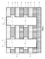
- Figure 8 illustrates top view of the a final stage of the three-dimensional memory arrays according to one embodiment of the present disclosure.
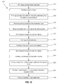
- the flowchart in figure 10 illustrates a method 200 comprising a plurality of manufacturing steps for a tree-dimensional resistive memory array in accordance with the present disclosure.
- Figure 1 illustrates a front view of a preliminary stage of a three-dimensional resistive memory array according an embodiment of the present disclosure.
- a substrate 100 has been provided according to step 202 of the method 200.
- the term substrate may include any underlying material or materials that may be used, or upon which a device according to embodiments of the present disclosure may be formed.
- this substrate may include a semiconductor substrate such as e.g.
- the substrate may further include, for example, an insulating layer such as a SiO 2 or a Si 3 N 4 layer in addition to a semiconductor substrate portion.
- an insulating layer such as a SiO 2 or a Si 3 N 4 layer in addition to a semiconductor substrate portion.
- the term substrate also includes silicon-on-glass, silicon-on sapphire substrates.
- the term substrate is thus used to define generally the elements of layers that underlie a layer or portions of interest.
- the substrate may be any other base on which a layer is formed, for example a glass or metal layer.
- the substrate may be made of any suitable material, the material of the substrate may be amorphous, polycrystalline or crystalline.
- Each stack of layers 102 comprises a repetitive sequence comprising an isolating layer 104, a semiconductor layer 106, a gate insulating layer 108 and a conductive layer 110.
- the stacks of layers 102 are provided in the step 204 of the method 200.
- the gate insulating layer 108 is arranged between the semiconductor layer 106 and the conductive layer 104.
- two stacks of layers 102 are illustrated for clarity although a person skilled in the art understands that any number of stacks of layers 102 may be arranged on top of each other in order to form the three-dimensional resistive memory array.
- An additional oxide layer 117 is further arranged on top of the stacks of layers 102.
- the layers in the stack of layers 102 may comprise conventional materials used in semiconductor industry.
- the isolating layer 104 may comprise an oxide such as for example SiO or a nitride such as for example SiN.
- the semiconductor layer 106 may comprise a semiconductor material such as for example Si, Ge or a III-V material.
- the gate insulating 108 layer may comprise SiO 2 or a dielectric material.
- the conductive layer 110 may comprise any material suitable for a gate electrode such as for example doped or undoped poly-Si, or a metal such as for example TiN, TaN, W.
- the stack of layers 102 may be formed using standard deposition techniques known to a person skilled in the art, such as, for example, chemical vapour phase deposition (CVD), more preferably, low pressure CVD (LPCVD) or similar.
- CVD chemical vapour phase deposition
- LPCVD low pressure CVD
- the additional layer 117 is provided optional in order to improve the electrical isolation and to protect the stack of layers 102 at the top of the three-dimensional resistive memory array. According to other embodiments the three-dimensional resistive memory array may be provided without the additional oxide layer 117.
- Figure 2 illustrates a preliminary stage of the three-dimensional resistive memory array disclosed in figure 1 , but after the stacks of layers 102 have been processed further.
- the processing has involved additional processing steps which will be described in the following.
- a plurality of parallel trenches 112 has been formed.
- the first step relates to step 206 of the method 200.
- the trenches 112 are extending through the stack of layers 102 to the front surface of the substrate 100.
- the trenches 112 have smooth vertical inner sidewalls 120 which for clarity are illustrated with dashed lines 120.
- the obtained trenches 112 are, in other words, elongated trenches or channels which extend in a parallel manner along the front side of the substrate 100.
- the trenches 112 will be described as being of a first type 114 and a second type 116. For clarity only one of each type of trenches 112 are illustrated in figure 2 . It should be noted that the three-dimensional resistive memory array may comprise any number of trenches 112 that are alternating of a first type 114 and a second type 116.
- the formation 206 of the plurality of trenches 112 may be achieved using standard process techniques known to a person skilled in the art.
- the standard process techniques may include, for example, lithographic steps comprising forming a hard mask layer of e.g. metal on the additional oxide layer 117 and a photoresist layer on top the hard mask layer.
- the hard mask may then subsequently be patterned.
- lithographic steps comprising forming a hard mask layer of e.g. metal on the additional oxide layer 117 and a photoresist layer on top the hard mask layer.
- the hard mask may then subsequently be patterned.
- a common approach is to expose and develop the photoresist such that selected portions of the hard mask are exposed.
- the exposed portions of the hardmask may then be removed by e.g. etching, using the photoresist as an etch mask.
- the plurality of trenches 112 may be formed in the stack of layers by etching through the stack of layers 102, using the hard mask layer
- This step comprises removing at least a portion of the conductive layer 110 in each sequence of the stack of layers 102 from inner side walls 120 of the first type 114 and the second type 116 of trenches 112 such that recesses 122 are formed in each sequence of the stack of layers 102.
- the process step corresponds to the step 208 of the method 200.
- the etching is preferably performed using an anisotropic etch process resulting in that mainly the conductive layer 110 is etched whereby the recesses 122 are formed.
- recesses 122 are formed in the previously smooth vertical inner side walls 120 of the trenches 112.
- Figure 3 illustrates the preliminary stage of the three-dimensional resistive memory array, disclosed in figures 1 and 2 , but after the trenches (and the recesses) of the first type 114 and the trenches (and the recesses) of the second type 116 have been filled with a first type of dielectric material 124. This filling corresponds to step 210 of the method 200. As illustrated in figure 3 , the recesses 122 are also filled with a first type of dielectric material 124.
- the first dielectric material 124 may comprises for example silicon oxide or silicon nitride which are standard material used in semiconductor industry. These materials are easy to handle and the filling of the trenches may be performed following standard recipes using standard processes.
- Figure 4 illustrates the preliminary stage of the three-dimensional resistive memory array, disclosed in figures 1 to 3 , after additional processing of the stack of layers 102 have been performed.
- the processes correspond to the steps 212 and 214 of the method 200 of figure 10 .
- the first type of dielectric material 124 in the first type of trenches 114 has been removed such that the side walls 120 of the trenches of the first type 114 are exposed.
- the first dielectric material 124 which is present in the recesses is not removed.
- a directional etching step is used for removing the first dielectric material 124 in the first type of trenches 114 .
- a metal oxide layer 126 has been formed on the exposed inner side walls 120 of the trenches of the first type 114. As illustrated in figure 4 , the metal oxide layer 126 is only partly filling the first type of trenches 114. In other words, a void space is present between the metal oxide layers 126 formed on the respective inner side walls 120 of the trenches of the first type 114.
- the metal oxide layer 126 is preferably deposited conformal along the trench. This may be done for example using atomic layer deposition (ALD). The metal oxide layer 126 is not deposited on the front surface of the substrate 100.
- the metal oxide layer 126 comprises a binary oxide from transition metals such as for example NiO, HfO, TaO, ZrO, AIO, NbO, TiO,...
- a binary oxide layer as a active layer or memory cell in a three-dimensional resistive memory array efficient switching of the resistance of the memory cell may be performed. In other words, is possible to switch the metal oxide layer between a high resistance state and a low resistance state which may be used for example to switch a RRAM back and forth between different memory states.
- the metal oxide layer 126 may comprise hafnium oxide which is known to show good switching characteristics, which is vital for using the metal oxide layer 126 as a active layer, also called memory cell, in non-volatile memory applications. Hafnium oxide is furthermore advantageous to use as it is a high-k dielectric.
- Figure 5 illustrates the preliminary stage of the three-dimensional resistive memory array disclosed in figures 1 to 4 , after additional processing steps have been made. The steps correspond to the step 216 and 218 of the method 200, respectively.
- a first type of conductive material 128 has been formed in the remaining portion or void space of the trenches of the first type 114.
- the first type of conductive material 128 may comprise semiconductors, metals, conductive oxides, metal nitrides and metal silicides. Hence, it is possible to use standard materials commonly used in semiconductor industry. In addition to that it is also possible to tailor the electric properties of the first type of conductive material 128 such that an efficient operation and desirable conducting properties of the conductive material 128 are obtained.
- This first type of conductive material 128 will function as a top electrode for the RRAM switching element.
- the first type of dielectric material 124 formed in the second type of trenches 116 has been removed such that the side walls 120 of the trenches of the second type 116 are exposed.
- the first dielectric material 124 which is present in the recesses is not removed.
- a directional etching step is used for removing the first dielectric material 124 in the second type of trenches 116 .
- Figure 6 illustrates a front view of the preliminary stage of the three-dimensional resistive memory array disclosed in figures 1 to 5 .
- a second type of conductive material 130 has been formed in the trenches of the second type 116.
- an electrical current may flow between the conducting material of the first type 128 and the second type 130 via a conducting layer 106 of the stack of layers 102.
- the function of the three-dimensional resistive memory array will further be described below.
- the forming of the conductive material of the second type 130 corresponds to the step 220 of the method 200.
- the second type of conductive material 130 may comprise the same materials as the first type of conductive material 128. To avoid undue repetition, reference is made to the discussion above. The first 128 and the second 130 type of conductive material may be the same as this simplifies the manufacturing of the three-dimensional resistive memory array.
- the integrated circuit 300 comprises a transistor device 302 which may be any of a MOSFET, a pinch-off FET or a FinFET.
- the transistor device 302 is a three-terminal device.
- the transistor device 302 may include a channel area extending in a direction substantially perpendicular to a surface of the substrate 100 onto which the stack of layers 102 is provided. A channel area may be formed in the semiconductor layer 106 in a conventional manner.
- the conductivity of the electrical path between a resistivity switching memory layer 310 formed by the metal oxide layer 126 and the conductive material of the first type 128 is controlled by the transistor device 302.
- the transistor device 302 is configured to switch on and/or off the current to the resistivity switching memory layer 310.
- the transistor device 302 may be formed in the semiconductor layer 106, e.g. a silicon layer, on top of the insulation layer 104.
- the conductive layer 110 acting as a gate electrode 304
- the gate insulating layer 108 is sandwiched and acts as a gate dielectric 306.
- an inversion or accumulation channel 308 may be formed in the semiconductor layer 106.
- the inversion or accumulation channel 308 may be used as a switchable electrode between the resistivity switching active layer 310, i.e. the memory cell of the resistive memory array and an electrode 312, By such an operation the resistivity, i.e. a stored value, of the resistivity switching active layer 310 may be changed such that the a memory state is changed.
- the conductive layer 110 may in each sequence of the repetitive sequence 102 be provided with a first isolation portion 400 arranged and a second isolation portion 402 arranged adjacent to the conductive layer 110.
- the isolation portions 400, 402 are numbered although the three-dimensional resistive memory array may comprise a plurality of isolation portions of the first and/or second type 400, 402, respectively.
- the presence of the isolation portion 400, 402 is advantageous as the conductive layer 110 may be electrically isolated from the metal oxide layer 126 in the trenches of the first type 114 and/or the second type of conductive material 130 in the trenches of the second type 116.
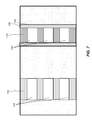
- Figure 7 also illustrates the preliminary stage of the three-dimensional resistive memory array disclosed in figure 1 to 6 , but now in a top view i.e. a view from a direction being perpendicular to the front surface of the substrate 100.
- Figure 7 further illustrates that in subsequent processing steps, corresponding to the steps 222 and 224 in the method 200, have been performed.
- a plurality of separated holes 132 extending through the stack of layers 102 has been formed in each trench of the first type 114.
- the metal oxide layer 126 formed on the inner side walls 120 of the trenches of the first type 114 has thereby been exposed.
- a plurality of separated holes 134 has further been formed in each trench of the second type 116 .
- the separated holes 134 also extend through the stack of layers 102.
- a three-dimensional structure is obtained. In the so formed three-dimensional structure the holes separate various regions of the stacks of layers 102.
- the three-dimensional resistive array may thereafter be formed by additionally filling the plurality of separated holes 132, 134 formed in the trenches of the first type 114 and the second type 116 with a second type of dielectric material 136.
- the step of filling the separated holes corresponds to step 226 of the method 200.
- Figure 8 illustrates the three-dimensional resistive memory array resulting from the above described processing steps.
- the structure of the obtained three-dimensional resistive memory array may be described by that it comprises an elongated stack of a repetitive sequence 102, each sequence comprising an isolating layer 104, a semiconductor layer 106, a gate insulating layer 108, and a conductive layer 110, the layers being stacked in a perpendicular direction with respect to a longitudinal direction of the elongated stack.
- the gate insulating layer 108 is arranged between the semiconductor layer 106 and the conductive layer 110.
- the semiconductor layer 106, the gate insulating layer 108, and the conductive layer 110 forms an array of selector transistors arranged along the longitudinal direction of the elongated stack, the elongated stack having a first side surface extending along and to the longitudinal direction of the elongated stack, and a second side surface being opposite to the first side surface.
- the first side surface of the elongated stack is provided with a metal oxide layer 126.
- the metal oxide layer 126 being provided with, on a surface facing away from the elongated stack, a second type of dielectric material 136 and a first type of conductive material 128, the second dielectric material 136 and the first type of conductive material 128 alternating along the longitudinal direction of the elongated stack,
- the second side surface of the elongated stack is provided with the second type of dielectric material 136 and a second type of conductive material 130, the second type of dielectric material 136 and the second type of conductive material 130 alternating along the longitudinal direction of the elongated stack.
- the method may further comprise the steps of removing the exposed metal oxide 126 formed on the inner side walls 120 of the trenches of the first type 114, such that the semiconductor layer 106 is at least partly exposed 138.
- the method may also comprise the step of at least partly removing the exposed semiconductor layer 106, 138.
- the metal oxide layer 126 may be provided at locations corresponding to the first type of conductive material 128, and the semiconductor layer 106 may be thinner at locations 139.
- parasitic conduction paths such as the illustrated parasitic path 140 may be counteracted.
- a more efficient direct current path 141 which regulates the function of the resistive memory array may be provided, which improves the performance of the three-dimensional resistive memory device.
- the provided separated holes 132, 134 preferably are filled with a dielectric material of the second type 136.
- the three-dimensional resistive memory array may further comprise an additional elongated stack of a repetitive sequence, wherein the first side surface of the elongated stack and the first side surface of the additional elongated stack are facing each other.
Landscapes
- Engineering & Computer Science (AREA)
- Manufacturing & Machinery (AREA)
- Semiconductor Memories (AREA)
Abstract
Description
- The present disclosure relates to a three-dimensional resistive memory array and a method for forming the same.
- There is a continuous need for increasing bit density and reducing bit cost in memory devices, and new alternatives are being proposed for ultra-high density memory technologies, such as, three-dimensional stacked resistive random-access memory (3D RRAM) devices.
- One possibility for advanced scaling of RRAM device in 3D consists of vertically stacking of horizontal planes, the horizontal planes each comprising a memory array with 1 selector and 1 RRAM cell. This is however a more pseudo-3D approach for which the manufacturing process is too costly. Another possibility is the so-called 3D RRAM BICS approach as for example disclosed in
US8,063,438 . A vertical-type RRAM device is disclosed including an insulation layer pattern of a linear shape provided on a substrate and pillar-shaped single-crystalline semiconductor patterns provided on both sidewalls of the insulation layer pattern and transistors provided, also in the vertical direction, on a sidewall of each of the single-crystalline semiconductor patterns. - There is a need for alternative solutions to manufacture 3D RRAM device which comprise a resistor and a selector, preferably a transistor (1T1R) in the cell.
- An object of the present disclosure is to provide an improved method for manufacturing a three-dimensional resistive memory (3D RRAM) array comprising a transistor selector in each cell (i.e. 1 T1 R cell). A further object is to provide an improved three-dimensional resistive memory array.
- According to a first aspect of the present disclosure a method for manufacturing a three-dimensional 1T-1 R resistive memory array is provided. The method comprises the steps of a) providing a substrate, b) forming a stack of layers arranged on top of each other on a front surface of the substrate, wherein the stack of layers comprises a repetitive sequence, each sequence comprising an isolating layer, a semiconductor layer, a gate insulating layer, and a conductive layer, wherein the gate insulating layer is arranged between the semiconductor layer and the conductive layer, c) forming a plurality of parallel trenches through the stack of layers, the trenches being alternating of a first type and a second type and extending along and to the front surface of the substrate, d) removing at least a portion of the conductive layer in each sequence of the stack of layers from inner side walls of the first type and the second type of trenches such that recesses are formed in each sequence of the stack of layers, e) filling the trenches of the first type and the second type, and the recesses with a first type of dielectric material, f) removing the first type of dielectric material formed in the first type of trenches thereby exposing the side walls of the trenches of the first type, g) forming a metal oxide layer on the exposed inner side walls of the trenches of the first type, wherein the metal oxide layer is partly filling the first type of trenches, h) forming a first type of conductive material in a remaining portion of the trenches of the first type, i) removing the first type of dielectric material formed in the second type of trenches, j) forming a second type of conductive material in the trenches of the second type, k) forming in each trench of the first type a plurality of separated holes extending through the stack of layers, and exposing the metal oxide layer formed on the inner side walls of the trenches of the first type, I) forming in each trench of the second type a plurality of separated holes extending through the stack of layers, m) filling the plurality of separated holes formed in the trenches of the first type and the second type with a second type of dielectric material.
- It is an advantage of the method of the present disclosure that a cost-effective fabrication flow may be used for manufacturing a three-dimensional resistive memory array with a 1T1R cell. The manufacturing of the three-dimensional 1T1R resistive memory array may further be performed using conventional processing steps, which reduces cost associated with the fabrication. Furthermore, the method is not dependent on stacking of prefabricated memory cells (so-called pseudo-3D) in order to achieve a three-dimensional memory array.
- The method may further comprise removing the exposed metal oxide formed on the inner side walls of the trenches of the first type, such that the semiconductor layer is at least partly exposed, and at least partly removing the exposed semiconductor layer.
- A more efficient resistive memory array may thereby be provided by the method as parasitic conduction resulting in undesired parasitic currents may be reduced by partly removing the exposed semiconductor layer. Further, the method allows improved device performance and facilitate high density packing of the of three-dimensional memory arrays.
- The isolating layer may comprise an oxide or a nitride, the semiconductor layer may comprise Si, Ge or a III-V material, the gate insulating layer may comprise SiO2 or a dielectric material and the conductive layer may comprise TiN, TaN, W or doped or undoped polySi. By using conventional materials efficient manufacturing processes or protocols to for example deposit and etch the materials of the three-dimensional memory array may be used.
- The method may further comprise the step of providing an additional oxide layer on top of the stack of layers. The
additional layer 117 improve the electrical isolation and protects the stack of layers at the top of the three-dimensional resistive memory array. - The first and/or second the type of dielectric material may comprise silicon oxide or silicon nitride, which facilitates efficient manufacturing of the resistive memory arrays.
- The metal oxide layer may comprise a binary oxide from transition metals. These materials are suitable for usages as resistive switching elements, i.e. as the active layer or memory cell of a memory device. The memory cell may thereby be formed in the metal oxide layer.
- The first and/or second type of conductive material may comprise a material selected from the group consisting of, semiconductors, metals, conductive oxides, metal nitrides and metal silicides.
- According to a second aspect of the present disclosure a three-dimensional resistive memory array is provided. The three-dimensional resistive memory array comprises A three-dimensional resistive memory array comprising an elongated stack of a repetitive sequence, each sequence comprising an isolating layer, a semiconductor layer, a gate insulating layer, and a conductive layer, the layers being stacked in a perpendicular direction with respect to a longitudinal direction of the elongated stack, wherein the gate insulating layer is arranged between the semiconductor layer and the conductive layer, wherein the semiconductor layer, the gate insulating layer, and the conductive layer forms an array of selector transistors arranged along the longitudinal direction of the elongated stack, the elongated stack having a first side surface extending along and to the longitudinal direction of the elongated stack, and a second side surface being opposite to the first side surface, wherein the first side surface of the elongated stack is provided with a metal oxide layer, the metal oxide layer being provided with, on a surface facing away from the elongated stack, a second type of dielectric material and a first type of conductive material, the second dielectric material and the first type of conductive material alternating along the longitudinal direction of the elongated stack, wherein the second side surface of the elongated stack is provided with the second type of dielectric material and a second type of conductive material, the second type of dielectric material and the second type of conductive material alternating along the longitudinal direction of the elongated stack.
- The conductive layer may in each sequence of the repetitive sequence may be provided with a first isolation portion arranged adjacent to the first side surface of the elongated stack and/or a second isolation portion arranged adjacent to the second side surface of the elongated stack. This is advantageous as a structure may be obtained in which the conductive layer is electrically isolated from the metal oxide layer in the trenches of the first type and/or the second type of conductive material in the trenches of the second type. In addition, leakage currents from the conductive materials to the metal oxide layer may be mitigated. An improved three-dimensional resistive memory array may thereby be obtained.
- The metal oxide layer may be provided at locations corresponding to the first type of conductive material alternating along the longitudinal direction of the elongated stack, and the semiconductor layer may be thinner at locations corresponding to the second type of dielectric material alternating along the longitudinal direction of the elongated stack. Parasitic conduction paths may thereby be mitigated such that an improved three-dimensional resistive memory array is obtained.
- The selector transistors may be junction less pinch off field effect transistors. This may allow for efficient control of charge carriers in the transistor such that a current flowing through transistor may easily be controlled.
- The three-dimensional resistive memory array may comprise an additional elongated stack of a repetitive sequence, wherein the first side surface of the elongated stack and the first side surface of the additional elongated stack are facing each other.
- Further features of, and advantages with, the present disclosure will become apparent when studying the appended claims and the following description. The skilled person will realize that different features of the present disclosure may be combined to create embodiments other than those described in the following, without departing from the scope of the present disclosure.
- This and other aspects of the present disclosure will now be described in more detail, with reference to the enclosed drawings showing embodiments of the disclosure.
-
Figure 1 illustrates a front view of a preliminary stage of a three-dimensional resistive memory array according to an embodiment of the present disclosure. -
Figure 2 illustrates a front view of a preliminary stage of a three-dimensional resistive memory array according to an embodiment of the present disclosure. -
Figure 3 illustrates a front view of a preliminary stage of a three-dimensional resistive memory array according to an embodiment of the present disclosure. -
Figure 4 illustrates a front view of a preliminary stage of a three-dimensional resistive memory array according to an embodiment of the present disclosure. -
Figure 5 illustrates a front view of a preliminary stage of a three-dimensional resistive memory array according to an embodiment of the present disclosure. -
Figure 6 illustrates a front view of a preliminary stage of a three-dimensional resistive memory array according to an embodiment of the present disclosure. -
Figure 7 illustrates a top view of a preliminary stage of a three-dimensional resistive memory array according to an embodiment of the present disclosure. -
Figure 8 illustrates a top view of a three-dimensional resistive memory array according to an embodiment of the present disclosure. -
Figure 9 illustrates a top view of a preliminary stage of a three-dimensional resistive memory array according to an embodiment of the present disclosure. -
Figure 10 illustrates a flowchart of the method according to the disclosure. - The present disclosure will now be described more fully hereinafter with reference to the accompanying drawings, in which currently preferred embodiments of the disclosure are shown. This disclosure may, however, be embodied in many different forms and should not be construed as limited to the embodiments set forth herein. These embodiments are rather provided for thoroughness and completeness, and for fully conveying the scope of the disclosure to the skilled person.
- A method for manufacturing a three-dimensional resistive memory array in accordance with the present disclosure will now be described with reference
figures 1 to 9 which illustrate a plurality of manufacturing steps in more detail.Figures 1 to 6 shows front views of preliminary stages of the three-dimensional resistive memory array, whereasfigures 7 to 9 provides top views of the same memory array.Figure 8 illustrates top view of the a final stage of the three-dimensional memory arrays according to one embodiment of the present disclosure. The flowchart infigure 10 illustrates amethod 200 comprising a plurality of manufacturing steps for a tree-dimensional resistive memory array in accordance with the present disclosure. -
Figure 1 illustrates a front view of a preliminary stage of a three-dimensional resistive memory array according an embodiment of the present disclosure. At the bottom of the layer structure shown infigure 1 asubstrate 100 has been provided according tostep 202 of themethod 200. In embodiments of the present disclosure, the term substrate may include any underlying material or materials that may be used, or upon which a device according to embodiments of the present disclosure may be formed. In particular embodiments, this substrate may include a semiconductor substrate such as e.g. a silicon, a gallium arsenide (GaAs), a gallium arsenide phosphide (GaAsP), an indium phosphide (InP), a germanium (Ge), or a silicon germanium (SiGe) substrate. The substrate may further include, for example, an insulating layer such as a SiO2 or a Si3N4 layer in addition to a semiconductor substrate portion. Thus, the term substrate also includes silicon-on-glass, silicon-on sapphire substrates. The term substrate is thus used to define generally the elements of layers that underlie a layer or portions of interest. Also, the substrate may be any other base on which a layer is formed, for example a glass or metal layer. As examples, the substrate may be made of any suitable material, the material of the substrate may be amorphous, polycrystalline or crystalline. - On top of the front surface of the
substrate 100 two stacks oflayers 102 are shown. Each stack oflayers 102 comprises a repetitive sequence comprising an isolatinglayer 104, asemiconductor layer 106, agate insulating layer 108 and aconductive layer 110. The stacks oflayers 102 are provided in thestep 204 of themethod 200. As can be seen infigure 1 thegate insulating layer 108 is arranged between thesemiconductor layer 106 and theconductive layer 104. Infigure 1 two stacks oflayers 102 are illustrated for clarity although a person skilled in the art understands that any number of stacks oflayers 102 may be arranged on top of each other in order to form the three-dimensional resistive memory array. Anadditional oxide layer 117 is further arranged on top of the stacks oflayers 102. - The layers in the stack of
layers 102 may comprise conventional materials used in semiconductor industry. The isolatinglayer 104 may comprise an oxide such as for example SiO or a nitride such as for example SiN. Thesemiconductor layer 106 may comprise a semiconductor material such as for example Si, Ge or a III-V material. The gate insulating 108 layer may comprise SiO2 or a dielectric material. Theconductive layer 110 may comprise any material suitable for a gate electrode such as for example doped or undoped poly-Si, or a metal such as for example TiN, TaN, W. By using conventional materials a three-dimensional resistive memory array may be provided in a cost efficient way. - The stack of
layers 102 may be formed using standard deposition techniques known to a person skilled in the art, such as, for example, chemical vapour phase deposition (CVD), more preferably, low pressure CVD (LPCVD) or similar. - It should be noted that the
additional layer 117 is provided optional in order to improve the electrical isolation and to protect the stack oflayers 102 at the top of the three-dimensional resistive memory array. According to other embodiments the three-dimensional resistive memory array may be provided without theadditional oxide layer 117. -
Figure 2 illustrates a preliminary stage of the three-dimensional resistive memory array disclosed infigure 1 , but after the stacks oflayers 102 have been processed further. The processing has involved additional processing steps which will be described in the following. In one step a plurality ofparallel trenches 112 has been formed. The first step relates to step 206 of themethod 200. Thetrenches 112 are extending through the stack oflayers 102 to the front surface of thesubstrate 100. Thetrenches 112 have smooth verticalinner sidewalls 120 which for clarity are illustrated with dashedlines 120. The obtainedtrenches 112 are, in other words, elongated trenches or channels which extend in a parallel manner along the front side of thesubstrate 100. In the following, thetrenches 112 will be described as being of afirst type 114 and asecond type 116. For clarity only one of each type oftrenches 112 are illustrated infigure 2 . It should be noted that the three-dimensional resistive memory array may comprise any number oftrenches 112 that are alternating of afirst type 114 and asecond type 116. - The
formation 206 of the plurality oftrenches 112 may be achieved using standard process techniques known to a person skilled in the art. The standard process techniques may include, for example, lithographic steps comprising forming a hard mask layer of e.g. metal on theadditional oxide layer 117 and a photoresist layer on top the hard mask layer. The hard mask may then subsequently be patterned. When patterning the hard mask layer a common approach is to expose and develop the photoresist such that selected portions of the hard mask are exposed. The exposed portions of the hardmask may then be removed by e.g. etching, using the photoresist as an etch mask. In the following the plurality oftrenches 112 may be formed in the stack of layers by etching through the stack oflayers 102, using the hard mask layer as an etch mask. The hard mask layer may then be removed using conventional methods. - Another step performed in order to obtain the preliminary stage of the three-dimensional resistive memory array shown in
figure 2 will now be described. This step comprises removing at least a portion of theconductive layer 110 in each sequence of the stack oflayers 102 frominner side walls 120 of thefirst type 114 and thesecond type 116 oftrenches 112 such that recesses 122 are formed in each sequence of the stack oflayers 102. The process step corresponds to thestep 208 of themethod 200. - The etching is preferably performed using an anisotropic etch process resulting in that mainly the
conductive layer 110 is etched whereby therecesses 122 are formed. In other words, as a result of anisotropic etching in the second process step recesses 122 are formed in the previously smooth verticalinner side walls 120 of thetrenches 112. -
Figure 3 illustrates the preliminary stage of the three-dimensional resistive memory array, disclosed infigures 1 and2 , but after the trenches (and the recesses) of thefirst type 114 and the trenches (and the recesses) of thesecond type 116 have been filled with a first type ofdielectric material 124. This filling corresponds to step 210 of themethod 200. As illustrated infigure 3 , therecesses 122 are also filled with a first type ofdielectric material 124. - The first
dielectric material 124 may comprises for example silicon oxide or silicon nitride which are standard material used in semiconductor industry. These materials are easy to handle and the filling of the trenches may be performed following standard recipes using standard processes. -
Figure 4 illustrates the preliminary stage of the three-dimensional resistive memory array, disclosed infigures 1 to 3 , after additional processing of the stack oflayers 102 have been performed. The processes correspond to thesteps method 200 offigure 10 . In one step the first type ofdielectric material 124 in the first type oftrenches 114 has been removed such that theside walls 120 of the trenches of thefirst type 114 are exposed. The firstdielectric material 124 which is present in the recesses is not removed. For removing the firstdielectric material 124 in the first type oftrenches 114 preferably a directional etching step is used. - In a following step a
metal oxide layer 126 has been formed on the exposedinner side walls 120 of the trenches of thefirst type 114. As illustrated infigure 4 , themetal oxide layer 126 is only partly filling the first type oftrenches 114. In other words, a void space is present between themetal oxide layers 126 formed on the respectiveinner side walls 120 of the trenches of thefirst type 114. Themetal oxide layer 126 is preferably deposited conformal along the trench. This may be done for example using atomic layer deposition (ALD). Themetal oxide layer 126 is not deposited on the front surface of thesubstrate 100. - The
metal oxide layer 126 comprises a binary oxide from transition metals such as for example NiO, HfO, TaO, ZrO, AIO, NbO, TiO,... By providing a binary oxide layer as a active layer or memory cell in a three-dimensional resistive memory array efficient switching of the resistance of the memory cell may be performed. In other words, is possible to switch the metal oxide layer between a high resistance state and a low resistance state which may be used for example to switch a RRAM back and forth between different memory states. In a preferred embodiment, themetal oxide layer 126 may comprise hafnium oxide which is known to show good switching characteristics, which is vital for using themetal oxide layer 126 as a active layer, also called memory cell, in non-volatile memory applications. Hafnium oxide is furthermore advantageous to use as it is a high-k dielectric. -
Figure 5 illustrates the preliminary stage of the three-dimensional resistive memory array disclosed infigures 1 to 4 , after additional processing steps have been made. The steps correspond to thestep method 200, respectively. - Firstly, a first type of
conductive material 128 has been formed in the remaining portion or void space of the trenches of thefirst type 114. The first type ofconductive material 128 may comprise semiconductors, metals, conductive oxides, metal nitrides and metal silicides. Hence, it is possible to use standard materials commonly used in semiconductor industry. In addition to that it is also possible to tailor the electric properties of the first type ofconductive material 128 such that an efficient operation and desirable conducting properties of theconductive material 128 are obtained. This first type ofconductive material 128 will function as a top electrode for the RRAM switching element. - Secondly, the first type of
dielectric material 124 formed in the second type oftrenches 116 has been removed such that theside walls 120 of the trenches of thesecond type 116 are exposed. The firstdielectric material 124 which is present in the recesses is not removed. For removing the firstdielectric material 124 in the second type oftrenches 116 preferably a directional etching step is used. -
Figure 6 illustrates a front view of the preliminary stage of the three-dimensional resistive memory array disclosed infigures 1 to 5 . Infigure 6 is illustrated that additionally a second type ofconductive material 130 has been formed in the trenches of thesecond type 116. Hence an electrical current may flow between the conducting material of thefirst type 128 and thesecond type 130 via aconducting layer 106 of the stack oflayers 102. The function of the three-dimensional resistive memory array will further be described below. The forming of the conductive material of thesecond type 130 corresponds to thestep 220 of themethod 200. - It should be noted that the second type of
conductive material 130 may comprise the same materials as the first type ofconductive material 128. To avoid undue repetition, reference is made to the discussion above. The first 128 and the second 130 type of conductive material may be the same as this simplifies the manufacturing of the three-dimensional resistive memory array. - The function of such a three-dimensional resistive memory array will now be described. Again referring to
figure 6 , the function of the three-dimensional resistive memory array is illustrated by a schematic circuit diagram 300. - The
integrated circuit 300 comprises atransistor device 302 which may be any of a MOSFET, a pinch-off FET or a FinFET. Thetransistor device 302 is a three-terminal device. Thetransistor device 302 may include a channel area extending in a direction substantially perpendicular to a surface of thesubstrate 100 onto which the stack oflayers 102 is provided. A channel area may be formed in thesemiconductor layer 106 in a conventional manner. - The conductivity of the electrical path between a resistivity
switching memory layer 310 formed by themetal oxide layer 126 and the conductive material of thefirst type 128 is controlled by thetransistor device 302. Thetransistor device 302 is configured to switch on and/or off the current to the resistivityswitching memory layer 310. - In more detail, the
transistor device 302 may be formed in thesemiconductor layer 106, e.g. a silicon layer, on top of theinsulation layer 104. At a top surface of thesemiconductor layer 106, theconductive layer 110, acting as agate electrode 304, is provided. Between thesemiconductor layer 106 and theconductive layer 110 thegate insulating layer 108 is sandwiched and acts as agate dielectric 306. By applying a suitable electrical signal to thegate electrode 304 an inversion oraccumulation channel 308 may be formed in thesemiconductor layer 106. The inversion oraccumulation channel 308 may be used as a switchable electrode between the resistivity switchingactive layer 310, i.e. the memory cell of the resistive memory array and anelectrode 312, By such an operation the resistivity, i.e. a stored value, of the resistivity switchingactive layer 310 may be changed such that the a memory state is changed. - Again referring to
figure 6 , it is illustrated that theconductive layer 110 may in each sequence of therepetitive sequence 102 be provided with afirst isolation portion 400 arranged and asecond isolation portion 402 arranged adjacent to theconductive layer 110. For clarity only theisolation portions second type isolation portion conductive layer 110 may be electrically isolated from themetal oxide layer 126 in the trenches of thefirst type 114 and/or the second type ofconductive material 130 in the trenches of thesecond type 116. -
Figure 7 also illustrates the preliminary stage of the three-dimensional resistive memory array disclosed infigure 1 to 6 , but now in a top view i.e. a view from a direction being perpendicular to the front surface of thesubstrate 100. -
Figure 7 further illustrates that in subsequent processing steps, corresponding to thesteps method 200, have been performed. In the first step a plurality of separatedholes 132 extending through the stack oflayers 102 has been formed in each trench of thefirst type 114. Themetal oxide layer 126 formed on theinner side walls 120 of the trenches of thefirst type 114 has thereby been exposed. In each trench of the second type 116 a plurality of separatedholes 134 has further been formed. The separatedholes 134 also extend through the stack oflayers 102. As a result of this processing a three-dimensional structure is obtained. In the so formed three-dimensional structure the holes separate various regions of the stacks oflayers 102. The three-dimensional resistive array may thereafter be formed by additionally filling the plurality of separatedholes first type 114 and thesecond type 116 with a second type ofdielectric material 136. The step of filling the separated holes corresponds to step 226 of themethod 200. -
Figure 8 , illustrates the three-dimensional resistive memory array resulting from the above described processing steps. The structure of the obtained three-dimensional resistive memory array may be described by that it comprises an elongated stack of arepetitive sequence 102, each sequence comprising an isolatinglayer 104, asemiconductor layer 106, agate insulating layer 108, and aconductive layer 110, the layers being stacked in a perpendicular direction with respect to a longitudinal direction of the elongated stack. Thegate insulating layer 108 is arranged between thesemiconductor layer 106 and theconductive layer 110. Thesemiconductor layer 106, thegate insulating layer 108, and theconductive layer 110 forms an array of selector transistors arranged along the longitudinal direction of the elongated stack, the elongated stack having a first side surface extending along and to the longitudinal direction of the elongated stack, and a second side surface being opposite to the first side surface. The first side surface of the elongated stack is provided with ametal oxide layer 126. Themetal oxide layer 126 being provided with, on a surface facing away from the elongated stack, a second type ofdielectric material 136 and a first type ofconductive material 128, the seconddielectric material 136 and the first type ofconductive material 128 alternating along the longitudinal direction of the elongated stack, The second side surface of the elongated stack is provided with the second type ofdielectric material 136 and a second type ofconductive material 130, the second type ofdielectric material 136 and the second type ofconductive material 130 alternating along the longitudinal direction of the elongated stack. - Now referring to
figure 9 , according to one embodiment of the present disclosure the method may further comprise the steps of removing the exposedmetal oxide 126 formed on theinner side walls 120 of the trenches of thefirst type 114, such that thesemiconductor layer 106 is at least partly exposed 138. The method may also comprise the step of at least partly removing the exposedsemiconductor layer - As a result the
metal oxide layer 126 may be provided at locations corresponding to the first type ofconductive material 128, and thesemiconductor layer 106 may be thinner atlocations 139. As a result parasitic conduction paths, such as the illustratedparasitic path 140 may be counteracted. By this process, a more efficient directcurrent path 141 which regulates the function of the resistive memory array may be provided, which improves the performance of the three-dimensional resistive memory device. - It should be noted that that the provided separated
holes second type 136. - The person skilled in the art realizes that the present disclosure by no means is limited to the preferred embodiments described above. On the contrary, many modifications and variations are possible within the scope of the appended claims.
- For example, the three-dimensional resistive memory array may further comprise an additional elongated stack of a repetitive sequence, wherein the first side surface of the elongated stack and the first side surface of the additional elongated stack are facing each other.
- Additionally, variations to the disclosed embodiments can be understood and effected by the skilled person in practicing the claimed disclosure, from a study of the drawings, the disclosure, and the appended claims. In the claims, the word "comprising" does not exclude other elements or steps, and the indefinite article "a" or "an" does not exclude a plurality. The mere fact that certain measures are recited in mutually different dependent claims does not indicate that a combination of these measures cannot be used to advantage. Also two or more steps may be performed concurrently or with partial concurrence. Further, the steps of the method may be performed in an order different from what has been disclosed. Such variation will depend on the process hardware systems chosen and on designer choice. All such variations are within the scope of the disclosure. Additionally, even though the disclosure has been described with reference to specific exemplifying embodiments thereof, many different alterations, modifications and the like will become apparent for those skilled in the art.
Claims (13)
- A method for manufacturing a three-dimensional resistive memory array, the method comprising the steps of:a) providing (202) a substrate (100),b) forming (204) a stack of layers (102) arranged on top of each other on a front surface of the substrate (100), wherein the stack of layers (102) comprises a repetitive sequence (102), each sequence (102) comprising an isolating layer (104), a semiconductor layer (106), a gate insulating layer (108), and a conductive layer (110), wherein the gate insulating layer (108) is arranged between the semiconductor layer (106) and the conductive layer (110),c) forming (206) a plurality of parallel trenches (112) through the stack of layers (102), the trenches (112) being alternating of a first type (114) and a second type (116) and extending along andto the front surface of the substrate (100),d) removing (208) at least a portion of the conductive layer (110) in each sequence (102) of the stack of layers (102) from inner side walls (120) of the first type (114) and the second type (116) of trenches (112) such that recesses (122) are formed in each sequence (102) of the stack of layers (102),e) filling (210) the trenches of the first type (114) and the second type (116), and the recesses (122) with a first type of dielectric material (124),f) removing (212) the first type of dielectric material (124) formed in the first type of trenches (114) thereby exposing the side walls (120) of the trenches of the first type (114) thereby leaving the recesses filled,g) forming (214) a metal oxide layer (126) on the exposed inner side walls (112) of the trenches of the first type (114), wherein the metal oxide layer (126) is partly filling the first type of trenches (114),h) forming (216) a first type of conductive material (128) in a remaining portion of the trenches of the first type (114),i) removing (218) the first type of dielectric material (124) formed in the second type of trenches (116),j) forming (220) a second type of conductive material (130) in the trenches of the second type (116),k) forming (222) in each trench of the first type (114) a plurality of separated holes (132) extending through the stack of layers (102), and exposing the metal oxide layer (126) formed (214) on the inner side walls (120) of the trenches of the first type (114),l) forming (224) in each trench of the second type (116) a plurality of separated holes (134) extending through the stack of layers (102),m) filling (226) the plurality of separated holes (132, 134) formed in the trenches of the first type (114) and the second type (116) with a second type of dielectric material (136).
- The method according to claim 1 further comprising,
removing the exposed metal oxide (126) formed (214) on the inner side walls (120) of the trenches of the first type (114), such that the semiconductor layer (106) is at least partly exposed (138), and
at least partly removing the exposed semiconductor layer (106, 138). - The method according to claim 1 or 2, wherein the isolating layer (104) comprises an oxide or a nitride, the semiconductor layer (106) comprises Si, Ge or a III-V material, the gate insulating layer (108) comprises SiO2 and the conductive layer (110) comprises TiN, TaN, W or doped or undoped polySi.
- The method according to any one of the preceding claims, the method further comprising the step of providing an additional oxide layer (117) on top of the stack of layers (102).
- The method according to any one of the preceding claims, wherein the first (124) and/or second (136) type of dielectric material comprises silicon oxide or silicon nitride.
- The method according to any one of the preceding claims, wherein the metal oxide layer (126) comprises a binary oxide from transition metals.
- The method according to claim 6 wherein the metal oxide layer (126) comprises any of NiO, HfO, TaO, ZrO, AIO, NbO, TiO.
- The method according to any one of the preceding claims, wherein the first (128) and/or second (130) type of conductive material comprises a material selected from the group consisting of, semiconductors, metals, conductive oxides, metal nitrides and metal silicides.
- A three-dimensional resistive memory array comprising:an elongated stack of a repetitive sequence (102), each sequence (102) comprising an isolating layer (104), a semiconductor layer (106), a gate insulating layer (108), and a conductive layer (110), the layers being stacked in a perpendicular direction with respect to a longitudinal direction of the elongated stack,
wherein the gate insulating layer (108) is arranged between the semiconductor layer (106) and the conductive layer (110),
wherein the semiconductor layer (106), the gate insulating layer (108), and the conductive layer (110) forms an array of selector transistors arranged along the longitudinal direction of the elongated stack, the elongated stack having a first side surface extending along and to the longitudinal direction of the elongated stack, and a second side surface being opposite to the first side surface,wherein the first side surface of the elongated stack is provided with a metal oxide layer (126),the metal oxide layer (126) being provided with, on a surface facing away from the elongated stack, a second type of dielectric material (136) and a first type of conductive material (128), the second dielectric material (136) and the first type of conductive material (128) alternating along the longitudinal direction of the elongated stack,wherein the second side surface of the elongated stack is provided with the second type of dielectric material (136) and a second type of conductive material (130), the second type of dielectric material (136) and the second type of conductive material (130) alternating along the longitudinal direction of the elongated stack. - The three-dimensional resistive memory array according to claim 9, wherein the conductive layer (110) in each sequence of the repetitive sequence (102) is provided with a first isolation portion (400) arranged adjacent to the first side surface of the elongated stack and/or a second isolation portion (402) arranged adjacent to the second side surface of the elongated stack.
- The three-dimensional resistive memory array according to claim 9 or 10,
wherein the metal oxide layer (126) is provided at locations corresponding to the first type of conductive material (128) alternating along the longitudinal direction of the elongated stack, and
wherein the semiconductor layer (106) being thinner at locations corresponding to the second type of dielectric material (136) alternating along the longitudinal direction of the elongated stack. - The three-dimensional resistive memory array according to any one of claims 9 to 11, wherein the selector transistors are junction less pinch off field effect transistors.
- The three-dimensional resistive memory array according to any one of claims 9 to 12, further comprising an additional elongated stack of a repetitive sequence (102), wherein the first side surface of the elongated stack and the first side surface of the additional elongated stack are facing each other.
Priority Applications (4)
| Application Number | Priority Date | Filing Date | Title |
|---|---|---|---|
| EP14150456.3A EP2887396B1 (en) | 2013-12-20 | 2014-01-08 | Three-dimensional resistive memory array |
| JP2014203418A JP6532207B2 (en) | 2013-12-20 | 2014-10-01 | Three-dimensional resistive memory array |
| KR1020140155381A KR101603852B1 (en) | 2013-12-20 | 2014-11-10 | Three-dimensional resistive memory array |
| US14/577,937 US9484389B2 (en) | 2013-12-20 | 2014-12-19 | Three-dimensional resistive memory array |
Applications Claiming Priority (2)
| Application Number | Priority Date | Filing Date | Title |
|---|---|---|---|
| EP13198989 | 2013-12-20 | ||
| EP14150456.3A EP2887396B1 (en) | 2013-12-20 | 2014-01-08 | Three-dimensional resistive memory array |
Publications (2)
| Publication Number | Publication Date |
|---|---|
| EP2887396A1 true EP2887396A1 (en) | 2015-06-24 |
| EP2887396B1 EP2887396B1 (en) | 2017-03-08 |
Family
ID=49920044
Family Applications (1)
| Application Number | Title | Priority Date | Filing Date |
|---|---|---|---|
| EP14150456.3A Active EP2887396B1 (en) | 2013-12-20 | 2014-01-08 | Three-dimensional resistive memory array |
Country Status (4)
| Country | Link |
|---|---|
| US (1) | US9484389B2 (en) |
| EP (1) | EP2887396B1 (en) |
| JP (1) | JP6532207B2 (en) |
| KR (1) | KR101603852B1 (en) |
Cited By (5)
| Publication number | Priority date | Publication date | Assignee | Title |
|---|---|---|---|---|
| FR3044823A1 (en) * | 2015-12-02 | 2017-06-09 | Commissariat Energie Atomique | TRANSISTOR DEVICE DISTRIBUTED TO MULTIPLE OVERLAPPED LEVELS INTEGRATING A RESISTIVE MEMORY |
| US9735202B1 (en) | 2016-02-16 | 2017-08-15 | Sandisk Technologies Llc | Implementation of VMCO area switching cell to VBL architecture |
| EP3440702A4 (en) * | 2016-04-01 | 2020-01-15 | Micron Technology, Inc. | THERMAL INSULATION FOR THREE-DIMENSIONAL MEMORY MATRICES |
| CN113675231A (en) * | 2020-05-14 | 2021-11-19 | 格芯新加坡私人有限公司 | Memory device and method of forming a memory device |
| EP3944327A1 (en) * | 2020-07-24 | 2022-01-26 | Taiwan Semiconductor Manufacturing Co., Ltd. | Memory device and manufacturing method thereof |
Families Citing this family (30)
| Publication number | Priority date | Publication date | Assignee | Title |
|---|---|---|---|---|
| US9425237B2 (en) | 2014-03-11 | 2016-08-23 | Crossbar, Inc. | Selector device for two-terminal memory |
| US10211397B1 (en) | 2014-07-07 | 2019-02-19 | Crossbar, Inc. | Threshold voltage tuning for a volatile selection device |
| US9633724B2 (en) | 2014-07-07 | 2017-04-25 | Crossbar, Inc. | Sensing a non-volatile memory device utilizing selector device holding characteristics |
| US9460788B2 (en) | 2014-07-09 | 2016-10-04 | Crossbar, Inc. | Non-volatile memory cell utilizing volatile switching two terminal device and a MOS transistor |
| US10115819B2 (en) | 2015-05-29 | 2018-10-30 | Crossbar, Inc. | Recessed high voltage metal oxide semiconductor transistor for RRAM cell |
| US9754888B2 (en) * | 2015-12-14 | 2017-09-05 | Toshiba Memory Corporation | Semiconductor memory device and method for manufacturing the same |
| US9728585B1 (en) | 2016-03-11 | 2017-08-08 | Kabushiki Kaisha Toshiba | Semiconductor memory device |
| US9876055B1 (en) | 2016-12-02 | 2018-01-23 | Macronix International Co., Ltd. | Three-dimensional semiconductor device and method for forming the same |
| JP2018157020A (en) | 2017-03-16 | 2018-10-04 | 東芝メモリ株式会社 | Storage device and manufacturing method thereof |
| US10096362B1 (en) | 2017-03-24 | 2018-10-09 | Crossbar, Inc. | Switching block configuration bit comprising a non-volatile memory cell |
| CN110660822B (en) | 2018-06-29 | 2024-11-26 | 三星电子株式会社 | Variable resistance memory device |
| CN112687717B (en) * | 2019-10-18 | 2024-03-08 | 华邦电子股份有限公司 | Variable resistance memory and manufacturing method thereof |
| US11177321B2 (en) * | 2019-10-23 | 2021-11-16 | Winbond Electronics Corp. | Resistive random access memories and method for fabricating the same |
| US11355697B2 (en) * | 2019-11-25 | 2022-06-07 | The Board Of Trustees Of The Leland Stanford Junior University | Nanometer scale nonvolatile memory device and method for storing binary and quantum memory states |
| US11776846B2 (en) * | 2020-02-07 | 2023-10-03 | Asm Ip Holding B.V. | Methods for depositing gap filling fluids and related systems and devices |
| US11532640B2 (en) | 2020-05-29 | 2022-12-20 | Taiwan Semiconductor Manufacturing Co., Ltd. | Method for manufacturing a three-dimensional memory |
| DE102020123746B4 (en) | 2020-05-29 | 2023-02-16 | Taiwan Semiconductor Manufacturing Co., Ltd. | Three-dimensional non-volatile memory device and method of making same |
| US11404091B2 (en) | 2020-06-19 | 2022-08-02 | Taiwan Semiconductor Manufacturing Co., Ltd. | Memory array word line routing |
| US11462686B2 (en) * | 2020-06-22 | 2022-10-04 | Nantero, Inc. | Three-dimensional array architecture for resistive change element arrays and methods for making same |
| US11640974B2 (en) | 2020-06-30 | 2023-05-02 | Taiwan Semiconductor Manufacturing Co., Ltd. | Memory array isolation structures |
| US11355516B2 (en) | 2020-07-16 | 2022-06-07 | Taiwan Semiconductor Manufacturing Co., Ltd. | Three-dimensional memory device and method |
| US11647634B2 (en) | 2020-07-16 | 2023-05-09 | Taiwan Semiconductor Manufacturing Co., Ltd. | Three-dimensional memory device and method |
| US11423966B2 (en) | 2020-07-30 | 2022-08-23 | Taiwan Semiconductor Manufacturing Co., Ltd. | Memory array staircase structure |
| TWI746137B (en) * | 2020-08-27 | 2021-11-11 | 華邦電子股份有限公司 | Memory structures and methods for forming the same |
| KR102845400B1 (en) | 2020-09-25 | 2025-08-13 | 삼성전자주식회사 | Variable resistance memory device |
| CN112599560B (en) * | 2020-12-14 | 2024-05-24 | 长江先进存储产业创新中心有限责任公司 | Semiconductor device and preparation method thereof |
| US12029049B2 (en) | 2020-12-16 | 2024-07-02 | Winbond Electronics Corp. | Memory structures and methods for forming the same |
| US12575113B2 (en) * | 2022-03-26 | 2026-03-10 | International Business Machines Corporation | High density memory with stacked nanosheet transistors |
| US20250159909A1 (en) * | 2023-11-15 | 2025-05-15 | Taiwan Semiconductor Manufacturing Company, Ltd. | Memory device and method of forming the same |
| US20250272058A1 (en) * | 2024-02-23 | 2025-08-28 | Micron Technology, Inc. | Three-Dimensional Phase-Change Memory Array Operable to Perform Multiplication Accumulation Operations |
Citations (4)
| Publication number | Priority date | Publication date | Assignee | Title |
|---|---|---|---|---|
| US20100237312A1 (en) * | 2009-03-19 | 2010-09-23 | Samsung Electronics Co., Ltd. | Nonvolatile memory device |
| US8063438B2 (en) | 2008-02-29 | 2011-11-22 | Samsung Electronics Co., Ltd. | Vertical-type semiconductor devices |
| US20130153847A1 (en) * | 2011-12-15 | 2013-06-20 | Nam Kyun PARK | Resistive memory device and method of manufacturing the same |
| US20130306933A1 (en) * | 2011-01-20 | 2013-11-21 | Micron Technology, Inc. | Nonvolatile Memory Cells and Arrays of Nonvolatile Memory Cells |
Family Cites Families (29)
| Publication number | Priority date | Publication date | Assignee | Title |
|---|---|---|---|---|
| JP5091491B2 (en) | 2007-01-23 | 2012-12-05 | 株式会社東芝 | Nonvolatile semiconductor memory device |
| JP2008277543A (en) | 2007-04-27 | 2008-11-13 | Toshiba Corp | Nonvolatile semiconductor memory device |
| JP5086851B2 (en) | 2008-03-14 | 2012-11-28 | 株式会社東芝 | Nonvolatile semiconductor memory device |
| JP4956598B2 (en) | 2009-02-27 | 2012-06-20 | シャープ株式会社 | Nonvolatile semiconductor memory device and manufacturing method thereof |
| US8546861B2 (en) * | 2009-03-05 | 2013-10-01 | Gwangju Institute Of Science And Technology | Resistance change memory device with three-dimensional structure, and device array, electronic product and manufacturing method therefor |
| KR101539699B1 (en) | 2009-03-19 | 2015-07-27 | 삼성전자주식회사 | Non-volatile memory device having three-dimensional structure and manufacturing method thereof |
| KR101603731B1 (en) | 2009-09-29 | 2016-03-16 | 삼성전자주식회사 | Vertical nand charge trap flash memory device and method for manufacturing same |
| JP5558090B2 (en) | 2009-12-16 | 2014-07-23 | 株式会社東芝 | Resistance variable memory cell array |
| KR101075494B1 (en) * | 2009-12-18 | 2011-10-21 | 주식회사 하이닉스반도체 | Vertical channel type non-volatile memory device and method for fabricating the same |
| US8508997B2 (en) | 2009-12-23 | 2013-08-13 | Intel Corporation | Multi-cell vertical memory nodes |
| KR20110093309A (en) | 2010-02-12 | 2011-08-18 | 주식회사 하이닉스반도체 | 3D structure nonvolatile memory device and method of manufacturing same |
| JP5450165B2 (en) | 2010-02-26 | 2014-03-26 | 株式会社東芝 | Nonvolatile semiconductor memory device and method of manufacturing nonvolatile semiconductor memory device |
| US8803214B2 (en) | 2010-06-28 | 2014-08-12 | Micron Technology, Inc. | Three dimensional memory and methods of forming the same |
| JP4921620B2 (en) | 2010-07-01 | 2012-04-25 | パナソニック株式会社 | Nonvolatile memory cell, nonvolatile memory cell array, and manufacturing method thereof |
| KR20120029291A (en) | 2010-09-16 | 2012-03-26 | 삼성전자주식회사 | Semiconductor devices and methods of fabricating the same |
| US8187932B2 (en) | 2010-10-15 | 2012-05-29 | Sandisk 3D Llc | Three dimensional horizontal diode non-volatile memory array and method of making thereof |
| KR101137928B1 (en) | 2010-10-22 | 2012-05-09 | 에스케이하이닉스 주식회사 | Method for fabricating non-volatile memory device |
| KR101171256B1 (en) | 2010-12-15 | 2012-08-07 | 에스케이하이닉스 주식회사 | Semiconductor Memory Device Having Resistive device |
| CN102544049B (en) | 2010-12-22 | 2014-04-16 | 中国科学院微电子研究所 | Three-dimensional semiconductor memory device and its manufacturing method |
| US8933491B2 (en) | 2011-03-29 | 2015-01-13 | Micron Technology, Inc. | Arrays of memory cells and methods of forming an array of vertically stacked tiers of memory cells |
| KR101794017B1 (en) | 2011-05-12 | 2017-11-06 | 삼성전자 주식회사 | Nonvolatile memory device and and fabricating method thereof |
| KR20120134869A (en) | 2011-06-03 | 2012-12-12 | 삼성전자주식회사 | Non-volatile memory device having resistance changeable element and method of forming the same |
| US8693241B2 (en) | 2011-07-13 | 2014-04-08 | SK Hynix Inc. | Semiconductor intergrated circuit device, method of manufacturing the same, and method of driving the same |
| KR20130015444A (en) | 2011-08-03 | 2013-02-14 | 삼성전자주식회사 | Non-volatile memory device and method for fabricating the device |
| KR101835114B1 (en) | 2011-09-07 | 2018-03-06 | 삼성전자주식회사 | Three Dimensional Semiconductor Device And Method Of Fabricating The Same |
| JP2013065638A (en) * | 2011-09-15 | 2013-04-11 | Elpida Memory Inc | Semiconductor device |
| US8395139B1 (en) | 2011-12-06 | 2013-03-12 | Nanya Technology Corp. | 1T1R resistive memory device and fabrication method thereof |
| JP2013197396A (en) * | 2012-03-21 | 2013-09-30 | Toshiba Corp | Semiconductor memory device and method of manufacturing the same |
| US8841649B2 (en) * | 2012-08-31 | 2014-09-23 | Micron Technology, Inc. | Three dimensional memory array architecture |
-
2014
- 2014-01-08 EP EP14150456.3A patent/EP2887396B1/en active Active
- 2014-10-01 JP JP2014203418A patent/JP6532207B2/en active Active
- 2014-11-10 KR KR1020140155381A patent/KR101603852B1/en active Active
- 2014-12-19 US US14/577,937 patent/US9484389B2/en active Active
Patent Citations (4)
| Publication number | Priority date | Publication date | Assignee | Title |
|---|---|---|---|---|
| US8063438B2 (en) | 2008-02-29 | 2011-11-22 | Samsung Electronics Co., Ltd. | Vertical-type semiconductor devices |
| US20100237312A1 (en) * | 2009-03-19 | 2010-09-23 | Samsung Electronics Co., Ltd. | Nonvolatile memory device |
| US20130306933A1 (en) * | 2011-01-20 | 2013-11-21 | Micron Technology, Inc. | Nonvolatile Memory Cells and Arrays of Nonvolatile Memory Cells |
| US20130153847A1 (en) * | 2011-12-15 | 2013-06-20 | Nam Kyun PARK | Resistive memory device and method of manufacturing the same |
Cited By (10)
| Publication number | Priority date | Publication date | Assignee | Title |
|---|---|---|---|---|
| FR3044823A1 (en) * | 2015-12-02 | 2017-06-09 | Commissariat Energie Atomique | TRANSISTOR DEVICE DISTRIBUTED TO MULTIPLE OVERLAPPED LEVELS INTEGRATING A RESISTIVE MEMORY |
| US9735202B1 (en) | 2016-02-16 | 2017-08-15 | Sandisk Technologies Llc | Implementation of VMCO area switching cell to VBL architecture |
| WO2017142790A1 (en) * | 2016-02-16 | 2017-08-24 | Sandisk Technologies Llc | Implementation of vmco area switching cell to vbl architecture |
| US10026782B2 (en) | 2016-02-16 | 2018-07-17 | Sandisk Technologies Llc | Implementation of VMCO area switching cell to VBL architecture |
| US10109679B2 (en) | 2016-02-16 | 2018-10-23 | Sandisk Technologies Llc | Wordline sidewall recess for integrating planar selector device |
| EP3440702A4 (en) * | 2016-04-01 | 2020-01-15 | Micron Technology, Inc. | THERMAL INSULATION FOR THREE-DIMENSIONAL MEMORY MATRICES |
| US10672835B2 (en) | 2016-04-01 | 2020-06-02 | Micron Technology, Inc. | Thermal insulation for three-dimensional memory arrays |
| US10847580B2 (en) | 2016-04-01 | 2020-11-24 | Micron Technology, Inc. | Thermal insulation for three-dimensional memory arrays |
| CN113675231A (en) * | 2020-05-14 | 2021-11-19 | 格芯新加坡私人有限公司 | Memory device and method of forming a memory device |
| EP3944327A1 (en) * | 2020-07-24 | 2022-01-26 | Taiwan Semiconductor Manufacturing Co., Ltd. | Memory device and manufacturing method thereof |
Also Published As
| Publication number | Publication date |
|---|---|
| KR20150073075A (en) | 2015-06-30 |
| JP2015122478A (en) | 2015-07-02 |
| KR101603852B1 (en) | 2016-03-15 |
| JP6532207B2 (en) | 2019-06-19 |
| US9484389B2 (en) | 2016-11-01 |
| EP2887396B1 (en) | 2017-03-08 |
| US20150179705A1 (en) | 2015-06-25 |
Similar Documents
| Publication | Publication Date | Title |
|---|---|---|
| US9484389B2 (en) | Three-dimensional resistive memory array | |
| TWI697106B (en) | Three-dimensional memory devices and fabricating methods thereof | |
| WO2020252892A1 (en) | Three-dimensional memory device with support structures in slit structures and method for forming the same | |
| KR101785154B1 (en) | Fin field effect transistor (finfet) device structure | |
| US10170548B2 (en) | Integrated capacitors with nanosheet transistors | |
| KR102272125B1 (en) | Semiconductor device and method | |
| CN107293640B (en) | Semiconductor device and method of forming the same | |
| JP7429085B2 (en) | Vertical transport fin field effect transistor combined with resistive memory structure | |
| CN113809093A (en) | Method of manufacturing a three-dimensional memory device | |
| CN109427774A (en) | Semiconductor device with a plurality of semiconductor chips | |
| TWI567981B (en) | Fin member structure and manufacturing method thereof | |
| US10777468B1 (en) | Stacked vertical field-effect transistors with sacrificial layer patterning | |
| KR20180069671A (en) | 2d material transistor with vertical structure | |
| US10971584B2 (en) | Low contact resistance nanowire FETs | |
| KR20200066548A (en) | Semiconductor device including memory cells and method for manufacturing thereof | |
| US12062713B2 (en) | Memory device and forming method thereof | |
| KR102755159B1 (en) | Semiconductor device and method of fabricating the same | |
| TW201733113A (en) | Semiconductor device | |
| CN109427889A (en) | Fin formula field effect transistor device and method | |
| TWI641147B (en) | Semiconductor device and method of manufacturing same | |
| CN113113407A (en) | Semiconductor device with a plurality of semiconductor chips | |
| JP2022027621A (en) | Semiconductor device structure and formation method for the same | |
| US20210111261A1 (en) | Semiconductor structures in a wide gate pitch region of semiconductor devices | |
| US9614037B2 (en) | Nano-ribbon channel transistor with back-bias control | |
| CN105633158A (en) | Semiconductor device manufacturing method |
Legal Events
| Date | Code | Title | Description |
|---|---|---|---|
| PUAI | Public reference made under article 153(3) epc to a published international application that has entered the european phase |
Free format text: ORIGINAL CODE: 0009012 |
|
| 17P | Request for examination filed |
Effective date: 20140108 |
|
| AK | Designated contracting states |
Kind code of ref document: A1 Designated state(s): AL AT BE BG CH CY CZ DE DK EE ES FI FR GB GR HR HU IE IS IT LI LT LU LV MC MK MT NL NO PL PT RO RS SE SI SK SM TR |
|
| AX | Request for extension of the european patent |
Extension state: BA ME |
|
| R17P | Request for examination filed (corrected) |
Effective date: 20151222 |
|
| RBV | Designated contracting states (corrected) |
Designated state(s): AL AT BE BG CH CY CZ DE DK EE ES FI FR GB GR HR HU IE IS IT LI LT LU LV MC MK MT NL NO PL PT RO RS SE SI SK SM TR |
|
| GRAP | Despatch of communication of intention to grant a patent |
Free format text: ORIGINAL CODE: EPIDOSNIGR1 |
|
| GRAS | Grant fee paid |
Free format text: ORIGINAL CODE: EPIDOSNIGR3 |
|
| INTG | Intention to grant announced |
Effective date: 20161110 |
|
| GRAA | (expected) grant |
Free format text: ORIGINAL CODE: 0009210 |
|
| AK | Designated contracting states |
Kind code of ref document: B1 Designated state(s): AL AT BE BG CH CY CZ DE DK EE ES FI FR GB GR HR HU IE IS IT LI LT LU LV MC MK MT NL NO PL PT RO RS SE SI SK SM TR |
|
| REG | Reference to a national code |
Ref country code: GB Ref legal event code: FG4D |
|
| REG | Reference to a national code |
Ref country code: CH Ref legal event code: EP Ref country code: AT Ref legal event code: REF Ref document number: 874239 Country of ref document: AT Kind code of ref document: T Effective date: 20170315 |
|
| REG | Reference to a national code |
Ref country code: IE Ref legal event code: FG4D |
|
| REG | Reference to a national code |
Ref country code: DE Ref legal event code: R096 Ref document number: 602014007271 Country of ref document: DE |
|
| REG | Reference to a national code |
Ref country code: LT Ref legal event code: MG4D |
|
| REG | Reference to a national code |
Ref country code: NL Ref legal event code: MP Effective date: 20170308 |
|
| PG25 | Lapsed in a contracting state [announced via postgrant information from national office to epo] |
Ref country code: HR Free format text: LAPSE BECAUSE OF FAILURE TO SUBMIT A TRANSLATION OF THE DESCRIPTION OR TO PAY THE FEE WITHIN THE PRESCRIBED TIME-LIMIT Effective date: 20170308 Ref country code: FI Free format text: LAPSE BECAUSE OF FAILURE TO SUBMIT A TRANSLATION OF THE DESCRIPTION OR TO PAY THE FEE WITHIN THE PRESCRIBED TIME-LIMIT Effective date: 20170308 Ref country code: LT Free format text: LAPSE BECAUSE OF FAILURE TO SUBMIT A TRANSLATION OF THE DESCRIPTION OR TO PAY THE FEE WITHIN THE PRESCRIBED TIME-LIMIT Effective date: 20170308 Ref country code: GR Free format text: LAPSE BECAUSE OF FAILURE TO SUBMIT A TRANSLATION OF THE DESCRIPTION OR TO PAY THE FEE WITHIN THE PRESCRIBED TIME-LIMIT Effective date: 20170609 Ref country code: NO Free format text: LAPSE BECAUSE OF FAILURE TO SUBMIT A TRANSLATION OF THE DESCRIPTION OR TO PAY THE FEE WITHIN THE PRESCRIBED TIME-LIMIT Effective date: 20170608 |
|
| REG | Reference to a national code |
Ref country code: AT Ref legal event code: MK05 Ref document number: 874239 Country of ref document: AT Kind code of ref document: T Effective date: 20170308 |
|
| PG25 | Lapsed in a contracting state [announced via postgrant information from national office to epo] |
Ref country code: BG Free format text: LAPSE BECAUSE OF FAILURE TO SUBMIT A TRANSLATION OF THE DESCRIPTION OR TO PAY THE FEE WITHIN THE PRESCRIBED TIME-LIMIT Effective date: 20170608 Ref country code: ES Free format text: LAPSE BECAUSE OF FAILURE TO SUBMIT A TRANSLATION OF THE DESCRIPTION OR TO PAY THE FEE WITHIN THE PRESCRIBED TIME-LIMIT Effective date: 20170308 Ref country code: SE Free format text: LAPSE BECAUSE OF FAILURE TO SUBMIT A TRANSLATION OF THE DESCRIPTION OR TO PAY THE FEE WITHIN THE PRESCRIBED TIME-LIMIT Effective date: 20170308 Ref country code: RS Free format text: LAPSE BECAUSE OF FAILURE TO SUBMIT A TRANSLATION OF THE DESCRIPTION OR TO PAY THE FEE WITHIN THE PRESCRIBED TIME-LIMIT Effective date: 20170308 Ref country code: LV Free format text: LAPSE BECAUSE OF FAILURE TO SUBMIT A TRANSLATION OF THE DESCRIPTION OR TO PAY THE FEE WITHIN THE PRESCRIBED TIME-LIMIT Effective date: 20170308 |
|
| PG25 | Lapsed in a contracting state [announced via postgrant information from national office to epo] |
Ref country code: NL Free format text: LAPSE BECAUSE OF FAILURE TO SUBMIT A TRANSLATION OF THE DESCRIPTION OR TO PAY THE FEE WITHIN THE PRESCRIBED TIME-LIMIT Effective date: 20170308 |
|
| PG25 | Lapsed in a contracting state [announced via postgrant information from national office to epo] |
Ref country code: RO Free format text: LAPSE BECAUSE OF FAILURE TO SUBMIT A TRANSLATION OF THE DESCRIPTION OR TO PAY THE FEE WITHIN THE PRESCRIBED TIME-LIMIT Effective date: 20170308 Ref country code: EE Free format text: LAPSE BECAUSE OF FAILURE TO SUBMIT A TRANSLATION OF THE DESCRIPTION OR TO PAY THE FEE WITHIN THE PRESCRIBED TIME-LIMIT Effective date: 20170308 Ref country code: CZ Free format text: LAPSE BECAUSE OF FAILURE TO SUBMIT A TRANSLATION OF THE DESCRIPTION OR TO PAY THE FEE WITHIN THE PRESCRIBED TIME-LIMIT Effective date: 20170308 Ref country code: SK Free format text: LAPSE BECAUSE OF FAILURE TO SUBMIT A TRANSLATION OF THE DESCRIPTION OR TO PAY THE FEE WITHIN THE PRESCRIBED TIME-LIMIT Effective date: 20170308 Ref country code: AT Free format text: LAPSE BECAUSE OF FAILURE TO SUBMIT A TRANSLATION OF THE DESCRIPTION OR TO PAY THE FEE WITHIN THE PRESCRIBED TIME-LIMIT Effective date: 20170308 |
|
| PG25 | Lapsed in a contracting state [announced via postgrant information from national office to epo] |
Ref country code: SM Free format text: LAPSE BECAUSE OF FAILURE TO SUBMIT A TRANSLATION OF THE DESCRIPTION OR TO PAY THE FEE WITHIN THE PRESCRIBED TIME-LIMIT Effective date: 20170308 Ref country code: PL Free format text: LAPSE BECAUSE OF FAILURE TO SUBMIT A TRANSLATION OF THE DESCRIPTION OR TO PAY THE FEE WITHIN THE PRESCRIBED TIME-LIMIT Effective date: 20170308 Ref country code: IS Free format text: LAPSE BECAUSE OF FAILURE TO SUBMIT A TRANSLATION OF THE DESCRIPTION OR TO PAY THE FEE WITHIN THE PRESCRIBED TIME-LIMIT Effective date: 20170708 Ref country code: PT Free format text: LAPSE BECAUSE OF FAILURE TO SUBMIT A TRANSLATION OF THE DESCRIPTION OR TO PAY THE FEE WITHIN THE PRESCRIBED TIME-LIMIT Effective date: 20170710 |
|
| REG | Reference to a national code |
Ref country code: DE Ref legal event code: R097 Ref document number: 602014007271 Country of ref document: DE |
|
| REG | Reference to a national code |
Ref country code: FR Ref legal event code: PLFP Year of fee payment: 5 |
|
| RAP2 | Party data changed (patent owner data changed or rights of a patent transferred) |
Owner name: IMEC VZW |
|
| PLBE | No opposition filed within time limit |
Free format text: ORIGINAL CODE: 0009261 |
|
| STAA | Information on the status of an ep patent application or granted ep patent |
Free format text: STATUS: NO OPPOSITION FILED WITHIN TIME LIMIT |
|
| PG25 | Lapsed in a contracting state [announced via postgrant information from national office to epo] |
Ref country code: DK Free format text: LAPSE BECAUSE OF FAILURE TO SUBMIT A TRANSLATION OF THE DESCRIPTION OR TO PAY THE FEE WITHIN THE PRESCRIBED TIME-LIMIT Effective date: 20170308 |
|
| 26N | No opposition filed |
Effective date: 20171211 |
|
| PG25 | Lapsed in a contracting state [announced via postgrant information from national office to epo] |
Ref country code: IT Free format text: LAPSE BECAUSE OF FAILURE TO SUBMIT A TRANSLATION OF THE DESCRIPTION OR TO PAY THE FEE WITHIN THE PRESCRIBED TIME-LIMIT Effective date: 20170308 Ref country code: SI Free format text: LAPSE BECAUSE OF FAILURE TO SUBMIT A TRANSLATION OF THE DESCRIPTION OR TO PAY THE FEE WITHIN THE PRESCRIBED TIME-LIMIT Effective date: 20170308 |
|
| REG | Reference to a national code |
Ref country code: CH Ref legal event code: PL |
|
| GBPC | Gb: european patent ceased through non-payment of renewal fee |
Effective date: 20180108 |
|
| PG25 | Lapsed in a contracting state [announced via postgrant information from national office to epo] |
Ref country code: LU Free format text: LAPSE BECAUSE OF NON-PAYMENT OF DUE FEES Effective date: 20180108 |
|
| REG | Reference to a national code |
Ref country code: IE Ref legal event code: MM4A |
|
| REG | Reference to a national code |
Ref country code: BE Ref legal event code: MM Effective date: 20180131 |
|
| PG25 | Lapsed in a contracting state [announced via postgrant information from national office to epo] |
Ref country code: LI Free format text: LAPSE BECAUSE OF NON-PAYMENT OF DUE FEES Effective date: 20180131 Ref country code: GB Free format text: LAPSE BECAUSE OF NON-PAYMENT OF DUE FEES Effective date: 20180108 Ref country code: CH Free format text: LAPSE BECAUSE OF NON-PAYMENT OF DUE FEES Effective date: 20180131 Ref country code: BE Free format text: LAPSE BECAUSE OF NON-PAYMENT OF DUE FEES Effective date: 20180131 |
|
| PG25 | Lapsed in a contracting state [announced via postgrant information from national office to epo] |
Ref country code: IE Free format text: LAPSE BECAUSE OF NON-PAYMENT OF DUE FEES Effective date: 20180108 |
|
| PG25 | Lapsed in a contracting state [announced via postgrant information from national office to epo] |
Ref country code: MC Free format text: LAPSE BECAUSE OF FAILURE TO SUBMIT A TRANSLATION OF THE DESCRIPTION OR TO PAY THE FEE WITHIN THE PRESCRIBED TIME-LIMIT Effective date: 20170308 |
|
| PG25 | Lapsed in a contracting state [announced via postgrant information from national office to epo] |
Ref country code: MT Free format text: LAPSE BECAUSE OF NON-PAYMENT OF DUE FEES Effective date: 20180108 |
|
| PG25 | Lapsed in a contracting state [announced via postgrant information from national office to epo] |
Ref country code: TR Free format text: LAPSE BECAUSE OF FAILURE TO SUBMIT A TRANSLATION OF THE DESCRIPTION OR TO PAY THE FEE WITHIN THE PRESCRIBED TIME-LIMIT Effective date: 20170308 |
|
| PG25 | Lapsed in a contracting state [announced via postgrant information from national office to epo] |
Ref country code: CY Free format text: LAPSE BECAUSE OF FAILURE TO SUBMIT A TRANSLATION OF THE DESCRIPTION OR TO PAY THE FEE WITHIN THE PRESCRIBED TIME-LIMIT Effective date: 20170308 Ref country code: HU Free format text: LAPSE BECAUSE OF FAILURE TO SUBMIT A TRANSLATION OF THE DESCRIPTION OR TO PAY THE FEE WITHIN THE PRESCRIBED TIME-LIMIT; INVALID AB INITIO Effective date: 20140108 Ref country code: MK Free format text: LAPSE BECAUSE OF NON-PAYMENT OF DUE FEES Effective date: 20170308 |
|
| PG25 | Lapsed in a contracting state [announced via postgrant information from national office to epo] |
Ref country code: AL Free format text: LAPSE BECAUSE OF FAILURE TO SUBMIT A TRANSLATION OF THE DESCRIPTION OR TO PAY THE FEE WITHIN THE PRESCRIBED TIME-LIMIT Effective date: 20170308 |
|
| REG | Reference to a national code |
Ref country code: DE Ref legal event code: R079 Ref document number: 602014007271 Country of ref document: DE Free format text: PREVIOUS MAIN CLASS: H01L0027240000 Ipc: H10B0063000000 |
|
| P01 | Opt-out of the competence of the unified patent court (upc) registered |
Effective date: 20230513 |
|
| PGFP | Annual fee paid to national office [announced via postgrant information from national office to epo] |
Ref country code: FR Payment date: 20251217 Year of fee payment: 13 |
|
| PGFP | Annual fee paid to national office [announced via postgrant information from national office to epo] |
Ref country code: DE Payment date: 20251217 Year of fee payment: 13 |