EP2887383A1 - Soi wafer manufacturing method - Google Patents
Soi wafer manufacturing method Download PDFInfo
- Publication number
- EP2887383A1 EP2887383A1 EP13863262.5A EP13863262A EP2887383A1 EP 2887383 A1 EP2887383 A1 EP 2887383A1 EP 13863262 A EP13863262 A EP 13863262A EP 2887383 A1 EP2887383 A1 EP 2887383A1
- Authority
- EP
- European Patent Office
- Prior art keywords
- wafer
- oxide film
- ion
- soi
- bond wafer
- Prior art date
- Legal status (The legal status is an assumption and is not a legal conclusion. Google has not performed a legal analysis and makes no representation as to the accuracy of the status listed.)
- Granted
Links
Images

Classifications
-
- H—ELECTRICITY
- H10—SEMICONDUCTOR DEVICES; ELECTRIC SOLID-STATE DEVICES NOT OTHERWISE PROVIDED FOR
- H10P—GENERIC PROCESSES OR APPARATUS FOR THE MANUFACTURE OR TREATMENT OF DEVICES COVERED BY CLASS H10
- H10P90/00—Preparation of wafers not covered by a single main group of this subclass, e.g. wafer reinforcement
- H10P90/19—Preparing inhomogeneous wafers
- H10P90/1904—Preparing vertically inhomogeneous wafers
- H10P90/1906—Preparing SOI wafers
- H10P90/1914—Preparing SOI wafers using bonding
- H10P90/1916—Preparing SOI wafers using bonding with separation or delamination along an ion implanted layer, e.g. Smart-cut
-
- H—ELECTRICITY
- H10—SEMICONDUCTOR DEVICES; ELECTRIC SOLID-STATE DEVICES NOT OTHERWISE PROVIDED FOR
- H10D—INORGANIC ELECTRIC SEMICONDUCTOR DEVICES
- H10D86/00—Integrated devices formed in or on insulating or conducting substrates, e.g. formed in silicon-on-insulator [SOI] substrates or on stainless steel or glass substrates
-
- H—ELECTRICITY
- H10—SEMICONDUCTOR DEVICES; ELECTRIC SOLID-STATE DEVICES NOT OTHERWISE PROVIDED FOR
- H10P—GENERIC PROCESSES OR APPARATUS FOR THE MANUFACTURE OR TREATMENT OF DEVICES COVERED BY CLASS H10
- H10P14/00—Formation of materials, e.g. in the shape of layers or pillars
- H10P14/60—Formation of materials, e.g. in the shape of layers or pillars of insulating materials
- H10P14/63—Formation of materials, e.g. in the shape of layers or pillars of insulating materials characterised by the formation processes
- H10P14/6302—Non-deposition formation processes
- H10P14/6304—Formation by oxidation, e.g. oxidation of the substrate
-
- H—ELECTRICITY
- H10—SEMICONDUCTOR DEVICES; ELECTRIC SOLID-STATE DEVICES NOT OTHERWISE PROVIDED FOR
- H10P—GENERIC PROCESSES OR APPARATUS FOR THE MANUFACTURE OR TREATMENT OF DEVICES COVERED BY CLASS H10
- H10P30/00—Ion implantation into wafers, substrates or parts of devices
- H10P30/20—Ion implantation into wafers, substrates or parts of devices into semiconductor materials, e.g. for doping
-
- H—ELECTRICITY
- H10—SEMICONDUCTOR DEVICES; ELECTRIC SOLID-STATE DEVICES NOT OTHERWISE PROVIDED FOR
- H10P—GENERIC PROCESSES OR APPARATUS FOR THE MANUFACTURE OR TREATMENT OF DEVICES COVERED BY CLASS H10
- H10P54/00—Cutting or separating of wafers, substrates or parts of devices
- H10P54/50—Cutting or separating of wafers, substrates or parts of devices by scoring, breaking or cleaving
- H10P54/52—Cutting or separating of wafers, substrates or parts of devices by scoring, breaking or cleaving by cleaving
-
- H—ELECTRICITY
- H10—SEMICONDUCTOR DEVICES; ELECTRIC SOLID-STATE DEVICES NOT OTHERWISE PROVIDED FOR
- H10P—GENERIC PROCESSES OR APPARATUS FOR THE MANUFACTURE OR TREATMENT OF DEVICES COVERED BY CLASS H10
- H10P90/00—Preparation of wafers not covered by a single main group of this subclass, e.g. wafer reinforcement
- H10P90/12—Preparing bulk and homogeneous wafers
- H10P90/16—Preparing bulk and homogeneous wafers by reclaiming or re-processing
-
- H—ELECTRICITY
- H10—SEMICONDUCTOR DEVICES; ELECTRIC SOLID-STATE DEVICES NOT OTHERWISE PROVIDED FOR
- H10P—GENERIC PROCESSES OR APPARATUS FOR THE MANUFACTURE OR TREATMENT OF DEVICES COVERED BY CLASS H10
- H10P90/00—Preparation of wafers not covered by a single main group of this subclass, e.g. wafer reinforcement
- H10P90/19—Preparing inhomogeneous wafers
- H10P90/1904—Preparing vertically inhomogeneous wafers
- H10P90/1906—Preparing SOI wafers
- H10P90/1914—Preparing SOI wafers using bonding
-
- H—ELECTRICITY
- H10—SEMICONDUCTOR DEVICES; ELECTRIC SOLID-STATE DEVICES NOT OTHERWISE PROVIDED FOR
- H10W—GENERIC PACKAGES, INTERCONNECTIONS, CONNECTORS OR OTHER CONSTRUCTIONAL DETAILS OF DEVICES COVERED BY CLASS H10
- H10W10/00—Isolation regions in semiconductor bodies between components of integrated devices
- H10W10/10—Isolation regions comprising dielectric materials
- H10W10/181—Semiconductor-on-insulator [SOI] isolation regions, e.g. buried oxide regions of SOI wafers
-
- H—ELECTRICITY
- H10—SEMICONDUCTOR DEVICES; ELECTRIC SOLID-STATE DEVICES NOT OTHERWISE PROVIDED FOR
- H10P—GENERIC PROCESSES OR APPARATUS FOR THE MANUFACTURE OR TREATMENT OF DEVICES COVERED BY CLASS H10
- H10P14/00—Formation of materials, e.g. in the shape of layers or pillars
- H10P14/60—Formation of materials, e.g. in the shape of layers or pillars of insulating materials
- H10P14/63—Formation of materials, e.g. in the shape of layers or pillars of insulating materials characterised by the formation processes
- H10P14/6302—Non-deposition formation processes
- H10P14/6322—Formation by thermal treatments
Definitions
- the present invention relates to a method for manufacturing an SOI wafer by the ion implantation delamination method.
- the SOI wafer warps in a convex shape on the delaminating plane side due to a buried oxide film which has been transferred from a surface of the bond wafer by the delamination heat treatment, whereas the bond wafer after delamination warps in a concave shape on the delaminating plane side in contrast to the SOI wafer because the front surface oxide film is separated and the oxide film remains only on the back surface.
- a magnitude of the warpage is determined depending on a thickness of the transferred oxide film, a contact between the SOI wafer and the bond wafer after delamination hardly occurs because magnitudes of the warpages of these wafers are almost the same.
- the bond wafer after delamination is formed into a shape obtained by subtracting the convex shape formed during the wafer processing from the concave shape due to the influence of the back surface oxide film.
- the ion implantation delamination method by the so-called coimplantation in which the ion implantation is performed by implanting two types of ion, for example, a hydrogen ion and a helium ion to form an ion-implanted layer at which delamination is caused, if the helium ion is implanted more deeply than the hydrogen ion, a helium ion-implanted layer remains in the bond wafer still after delamination while a hydrogen ion-implanted layer is divided into an SOI side and the bond wafer after delamination because the delamination is caused at the hydrogen ion-implanted layer.
- two types of ion for example, a hydrogen ion and a helium ion to form an ion-implanted layer at which delamination is caused
- warping force by which the bond wafer after delamination is warped so as to have a convex shape operates on the bond wafer after delamination by existence of the helium ion-implanted layer, thereby causing the mismatch in warp shape with the SOI wafer.
- Patent Document 1 Japanese Unexamined Patent publication (Kokai) No. 2009-283582
- the present inventors keenly conducted studies the above-mentioned method for manufacturing an SOI wafer by the ion implantation delamination method, and consequently found that, in the manufactured SOI wafer, SOI film thickness abnormalities in which a portion having a thin SOI film thickness is generated at a center portion of the SOI wafer are caused, and scratches occur at the thin film portion as shown in FIG. 4 .
- the present invention was accomplished in view of the above-described problems. It is an object of the present invention to provide a method for manufacturing an SOI wafer that can inhibit scratches and SOI film thickness abnormalities.
- the present invention provides a method for manufacturing an SOI wafer, comprising: implanting one or more gas ion selected from a hydrogen ion and a rare gas ion into a bond wafer composed of a semiconductor single crystal substrate from a surface of the bond wafer to form an ion-implanted layer; bonding the surface from which the ion is implanted into the bond wafer and a surface of a base wafer through an oxide film; and then delaminating the bond wafer at the ion-implanted layer by performing a delamination heat treatment with a heat treatment furnace to form the SOI wafer, wherein after the delamination heat treatment, a temperature of the heat treatment furnace is decreased to 250°C or less at temperature-decreasing rate of less than 3.0°C/min, and then the SOI wafer and the bond wafer after delamination are taken out from the heat treatment furnace.
- the temperature inside the heat treatment furnace during taking out the SOI wafer and the bond wafer of 250°C or less enables the formation of an oxide film during taking out the wafers to be inhibited. Even if a tip part of the convex shape of the SOI wafer is in contact with the bond wafer after delamination because of the mismatch, the occurrence of the conventional film thickness abnormalities at the tip part of the convex shape of the SOI wafer can be inhibited since the formation of the oxide film during taking out the wafers is inhibited on all surfaces of the wafer from the beginning.
- the temperature-decreasing rate of less than 3.0°C/min enables a temperature distribution of the wafer surface to be small during decreasing the temperature, so that a deformation of the wafer due to the temperature distribution can be reduced. Therefore, the occurrence of scratches of the SOI wafer can be inhibited.
- the present invention enables an SOI wafer in which scratches and SOI film thickness abnormalities are inhibited to be obtained.
- a semiconductor single crystal substrate having a front surface oxide film and a back surface oxide film may be prepared as the bond wafer for forming the ion-implanted layer to implant the ion through the front surface oxide film, the back surface oxide film being thicker than the front surface oxide film.
- the bond wafer after delamination is formed into a concave shape by a difference in film thickness among the oxide films, therefore the mismatch in warp shape between the SOI wafer and the bond wafer after delamination can be prevented, and the occurrence of scratches and SOI film thickness abnormalities due to the contact can be more greatly inhibited.
- a wafer may be used as the semiconductor single crystal substrate having the back surface oxide film thicker than the front surface oxide film, the wafer being manufactured by forming a thermal oxide film on all surfaces of a semiconductor single crystal substrate, then removing a portion of the thermal oxide film on a front surface side to obtain a semiconductor single crystal substrate having the thermal oxide film only on a back surface side thereof, and thermally oxidizing the semiconductor single crystal substrate having the thermal oxide film only on the back surface side.
- the difference in film thickness between the oxide film on the front surface that will become a surface to be bonded and the oxide film on the back surface can be appropriately adjusted.
- the front surface side on which the portion of the thermal oxide film has been removed may be polished.
- a wafer manufactured by subjecting the bond wafer delaminated at the ion-implanted layer to a reclaiming process may be used as the semiconductor single crystal substrate having the back surface oxide film thicker than the front surface oxide film.
- the reclaiming process may be performed without removing the back surface oxide film of the delaminated bond wafer.
- the ion implantation may be performed by a coimplantation of a hydrogen ion and a helium ion such that the helium ion is implanted more deeply than the hydrogen ion.
- the present invention can suppress the influence on warping of the bond wafer after delamination due to existence of the helium ion-implanted layer, and thereby prevent the mismatch in warp shape between the SOI wafer and the bond wafer after delamination, even if the helium ion is implanted more deeply than the hydrogen ion.
- the present invention can prevent the contact between the SOI wafer and the bond wafer after delamination due to the mismatch in relation to the delamination heat treatment in the ion implantation delamination method.
- a formation irregularity of the oxide film during taking out the wafers from the heat treatment furnace can be prevented even if the mismatch is caused. In this way, the occurrence of scratches and SOI film thickness abnormalities at the tip part of the convex shape of the SOI wafer can be inhibited.
- the present inventors found that, in the delamination heat treatment of the ion implantation delamination method for manufacturing an SOI wafer, if a magnitude of the concave shape of the bond wafer after delamination (the delaminated bond wafer) is smaller than that of the convex shape of the SOI wafer, a mismatch in warp shape is caused between the delaminated bond wafer and the SOI wafer, a tip part of the convex shape of the SOI layer surface is thereby brought into contact with the delaminated bond wafer in the delamination heat treatment process, and scratches and SOI film thickness abnormalities are likely to occur at a center portion of the SOI wafer and the like.
- the SOI wafer warps convexly toward the delaminating plane side in proportion to the film thickness of the buried oxide film.
- the delaminating plane side warps concavely by action of the oxide film on the back surface because the oxide film on the front surface is separated by the delamination.
- a magnitude of the convex shape of the SOI wafer is usually equal to a magnitude of the concave shape of the delaminated bond wafer, so that the tip part of the convex shape of the SOI wafer is hardly in contact with the delaminated bond wafer.
- mismatch possibly occurs, for example, by the influence of a warp shape formed in wafer processing.
- the present inventors investigated a mechanism of causing film thickness abnormalities.
- the take-out temperature inside the heat treatment furnace is set at 250°C or less to inhibit the formation of an oxide film on the SOI wafer surface in order to improve non-uniformity in thickness of the oxide film to be formed on the SOI layer surface after delamination. If the wafers are taken out from the furnace at a temperature exceeded 250°C, an oxide film is formed on the SOI wafer surface by oxygen contained in air. Therefore, non-uniformity in oxide film thickness between the wafer contact portion and the noncontact portion is caused.
- the take-out temperature of 250°C or less can inhibit the oxide film from being formed on the surface during taking out the wafers from the beginning, thereby minimize an oxide film thickness distribution of the wafer surface. Si etching is therefore performed uniformly in a plane in the subsequent SC1 cleaning, and the occurrence of the conventional film thickness abnormalities can be inhibited.
- the temperature-decreasing rate of less than 3.0°C/min at which the temperature is decreased to the take-out temperature of 250°C or less after the SOI layer is delaminated in the delamination heat treatment can minimize a temperature distribution of the wafer surface during decreasing the temperature, and inhibit scratching of the SOI wafer and the delaminated bond wafer due to a deformation of the wafer. If the temperature-decreasing rate is 3.0°C/min or more, a radial temperature distribution during decreasing the temperature is increased, and scratches easily occur because the wafer is deformed by a difference in thermal expansion coefficients.
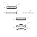
- FIG. 1 shows an example of the inventive method for manufacturing an SOI wafer.
- a semiconductor single crystal substrate 2 is prepared as the bond wafer 1 to form an oxide film 3 ( FIG. 1 at (A) ).
- the semiconductor single crystal substrate used as the bond wafer is preferably a silicon single crystal wafer.
- a germanium single crystal wafer, a germanium epitaxial wafer, an SiGe epitaxial wafer, a strained silicon wafer or an SiC single crystal wafer can also be used alternatively.
- the case of using a silicon single crystal wafer is described.
- a method for forming the oxide film 3 is not particularly limited to, the oxide film may be formed by thermal oxidation, for example.
- ions are implanted into the semiconductor single crystal substrate 1 having the oxide film 3 formed thereon from a side to be bonded (a front surface side) to form an ion-implanted layer ( FIG. 1 at (B) ).
- the ion-implanted layer may be, for example, a layer formed by implanting one or more gas ion selected from a hydrogen ion and a rare gas ion.
- a hydrogen ion-implanted layer 4 the case of implanting hydrogen ions (a hydrogen ion-implanted layer 4) is described as an example.
- the surface from which the ions are implanted into the bond wafer 1 and a surface of the base wafer 5 are bonded through the oxide film 3, for example, at room temperature of from 20 to 30°C to form a bonded wafer 6 ( FIG. 1 at (C) and (D) ).
- a plasma treatment may also be performed on a surface to be bonded of at least one of the bond wafer and the base wafer before bonding to increase the bonding strength obtained at room temperature.
- a silicon single crystal wafer or a silicon single crystal wafer on which an insulator film has been formed can be used, for example.
- the delamination heat treatment temperature may be, for example, 400°C or more, preferably from 400 to 600°C. The temperature in the above range enables the bonded wafer 6 to be appropriately delaminated at the hydrogen ion-implanted layer 4, and thereby a delaminated bond wafer 1' and an SOI wafer 8 having an SOI layer 7 can be obtained ( FIG. 1 at (E) ).
- a batch type furnace can be used as the heat treatment furnace, for example.
- the delamination heat treatment can be appropriately performed on wafers and a temperature inside the furnace can be decreased at a later-explained temperature-decreasing rate.
- a temperature inside the heat treatment furnace is decreased at a rate of less than 3.0°C/min.
- the SOI wafer 8 and the delaminated bond wafer 1' are then taken out under the temperature decreased to 250°C or less.
- the decreasing of the temperature at the rate of less than 3.0°C/min can reduce a temperature distribution of each wafer surface during decreasing the temperature, and inhibit scratching of the SOI wafer 8 and the delaminated bond wafer 1' due to a deformation of the wafer. Therefore, the occurrence of scratches can be prevented.
- the temperature-decreasing rate is preferably 2.5°C/min or less.
- a lower limit thereof is not particularly limited to, but preferably 1.0°C/min or more to perform the heat treatment process efficiently.
- the take-out temperature of 250°C or less can inhibit an oxide film from being formed on the surface during taking out the wafers. Therefore, even if a mismatch between the SOI wafer 8 and the delaminated bond wafer 1' is caused, there is no possibility that the oxide film in a tip part of the convex shape of the SOI wafer is formed thinly than other portion unlike in the conventional manner, and a radial oxide film thickness distribution can be minimized. Therefore, a formation irregularity of the oxide film thickness can be inhibited, Si etching is uniformly performed in a radial direction by the subsequent step of SC1 cleaning, and the occurrence of the conventional film thickness abnormalities of the SOI wafer can be prevented.
- the bond wafer As the bond wafer, the case of using the semiconductor single crystal substrate in which a thermal oxide film is merely formed on all surfaces thereof has been described.
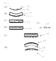
- the present invention can also use a semiconductor single crystal substrate having a back surface oxide film thicker than a front surface oxide film (an oxide film formed on the side to be bonded) as the bond wafer. This case is now described with reference to FIG. 2 .
- an oxide film 23' is formed on a back surface of a semiconductor single crystal substrate 22 ( FIG. 2 at (A) ).
- the oxide film 23' on the back surface is preferably a thermal oxide film, for example.
- a preferable method for forming the same is to manufacture a bond wafer having a thermal oxide film only on the back surface by forming a thermal oxide film on all surfaces of the bond wafer, and then removing a portion of the thermal oxide film on the side to be bonded of the bond wafer.
- Other methods for forming the oxide film 23' on the back surface include a method in which after forming a thermal oxide film having almost uniform thickness on all surfaces of the semiconductor single crystal substrate, while a part of the oxide film on the back surface is protected by a ring-shaped rubber (O-ring) or a protective sheet such as PVC, the semiconductor single crystal substrate is brought into contact with an etching solution for oxide film, or a method in which a part of the thermal oxide film is removed on the side to be bonded with a solution containing hydrogen fluoride (HF) by a spin etching etc. to remain the oxide film only on the back surface.
- a ring-shaped rubber O-ring
- a protective sheet such as PVC
- Another oxide film is formed on the semiconductor single crystal substrate 22 having the oxide film 23' formed on the back surface ( FIG. 2 at (B) ).
- Another oxide film is preferably a thermal oxide film.
- a preferable method for forming the same is to thermally oxidize all surfaces of the bond wafer having the back surface oxide film formed thereon. In this way, the wafer having the oxide film 23 in which the back surface side is thicker than the front surface side that will become the surface to be bonded of the semiconductor single crystal substrate 22 can be obtained.
- the bond wafer 21 having an oxide film different in thickness in front and back is thus manufactured.
- the method may comprise a step of polishing the side to be bonded by using chemical mechanical polishing (CMP) etc. after removing the oxide film on the side to be bonded, and then thermal oxidation may be performed on all surfaces ( FIG. 2 between (A) and (B)).
- CMP chemical mechanical polishing
- the bond wafer 21 in which the oxide film on the back surface is thicker than the oxide film on the front surface that will become the surface to be bonded can be previously formed into a concave shape before boding to the base wafer, and thereby the contact between the delaminated bond wafer and the SOI wafer can be inhibited. Moreover, this can inhibit the bond wafer from excessively warping and having a convex shape, thereby enabling the inhibition of the occurrence of the mismatch, even if a helium ion-implanted layer is formed as explained later.
- a degree of how thickly the oxide film on the back surface is formed compared with the oxide film on the surface to be bonded can be appropriately determined by experiments and calculations based on specifications of the SOI wafer to be manufactured (such as diameter, base wafer thickness and BOX layer thickness) and specifications of the bond wafer to be used (such as diameter and wafer thickness) so as to prevent the mismatch just after delamination (so that a magnitude of the convex shape of the SOI wafer is equal to a magnitude of the concave shape of the delaminated bond wafer).
- ions are implanted into the bond wafer 21 having the oxide film 23 formed thereon from the side to be bonded (the front surface side) to form an ion-implanted layer.
- a coimplantaion using hydrogen ions and helium ions is performed as the ion implantation, first, hydrogen ions are implanted to form a hydrogen ion-implanted layer 24 ( FIG. 2 at (C) ). Next, it is preferable that helium ions are implanted more deeply than the hydrogen ion-implanted layer 24 to form a helium ion-implanted layer 24' ( FIG. 2 at (D) ).
- the coimplantation thus performed can reduce an amount of ions to be implanted compared with the case of implanting one type of ions.
- the delaminated bond wafer is formed into convex shape by existence of the helium ion-implanted layer, so that the mismatch in warp shape with the SOI wafer occurs, resulting in scratches and SOI film thickness abnormalities.
- the thick thickness of the oxide film on the back surface enables the warp shape of the bond wafer to be previously adjusted before bonding, thereby the influence by existence of the helium ion-implanted layer 24' can be minimized.
- the surface from which the ions are implanted into the bond wafer 21 and a surface of the base wafer 25 are bonded through the oxide film 23, for example, at room temperature of from 20 to 30°C to form a bonded wafer 26 ( FIG. 2 at (E) and (F) ).
- the bond wafer is delaminated from the bonded wafer 26 at the hydrogen ion-implanted layer 24 by the delamination heat treatment so as to obtain a delaminated bond wafer 21', and thereby forming an SOI wafer 28 having an SOI layer 27 ( FIG. 2 at (G) ).
- the delamination heat treatment conditions may be set, for example, as in the first embodiment.
- the delaminated bond wafer 21' warps in a concave shape more reliably, and the conventional contact due to the mismatch in shape between the delaminated bond wafer and the SOI wafer can be prevented.
- the method for manufacturing an SOI wafer by the ion implantation delamination method is also characterize by being capable of reusing a delaminated bond wafer. Therefore, the present invention can also use a wafer manufactured by subjecting the delaminated bond wafer 21' and the like to a reclaiming process as the bond wafer. Thus, it is advantageous in a cost.
- the delaminated bond wafer is reclaimed by performing the reclaiming process without removing the oxide film on the back surface to manufacture a bond wafer having an oxide film on the back surface.
- the resultant wafer is then thermally oxidized, and thereby the bond wafer in which the oxide film on the back surface is thicker than the oxide film on the surface to be bonded can be easily manufactured.
- a removal of the oxide film remaining on an outer circumferential unbonded portion on the side to be bonded may be accomplished by directly polishing the side to be bonded.
- the removal may be performed using a method in which the delaminated bond wafer is brought into contact with an etching solution for oxide film while a part of the oxide film on the back surface is protected by a ring-shaped rubber (O-ring) or a protective sheet such as PVC, or using a spin etching machine.
- the back surface oxide film may be protected by blocking an etching solution or an etching gas by means of an O-ring, or by attaching a protective sheet, such as PVC, to the back surface of the delaminated bond wafer, as described above.
- a possible alternative way is performed such that an etching solution or an etching gas does not reach the back surface of the bond wafer because of wind pressure and centrifugal force generated by the rotation of the wafer.
- the etching solution for oxide film is preferably a HF solution.
- the etching may be performed with a HF gas.
- the O-ring is desirably provided at a position several millimeters from the outer circumference to warp the bond wafer. Depending on a permissible level of warping, however, it may be provided within the inside of this range.
- a bond wafer consisting of a 300-mm-diameter silicon single crystal wafer both surfaces of which have been mirror-polished was thermally oxidized to form a 30-nm-thickness thermal oxide film on all surfaces thereof, and subjected to the hydrogen ion-implantation though the thermal oxide film.
- the resultant bond wafer was bonded to a base wafer consisting of a 300-mm-diameter silicon single crystal wafer to manufacture a bonded wafer.
- the delamination heat treatment was then performed (at 500°C, for 30min, in nitrogen atmosphere) to delaminate a part of the bond wafer from the bonded wafer so that an SOI wafer was manufactured, and subjected to an SC1 cleaning.
- Example 1 Temperature-decreasing rate: 2.0°C/min, Take-out temperature: 250°C; Comparative Example 1 Temperature-decreasing rate: 3.0°C/min, Take-out temperature: 250°C; Comparative Example 2 Temperature-decreasing rate: 3.0°C/min, Take-out temperature: 225°C; Comparative Example 3 Temperature-decreasing rate: 3.0°C/min, Take-out temperature: 500°C; Comparative Example 4 Temperature-decreasing rate: 3.0°C/min, Take-out temperature: 360°C; Comparative Example 5 Temperature-decreasing rate: 3.0°C/min, Take-out temperature: 295°C; Comparative Example 6 Temperature-decreasing rate: 5.0°C/min, Take-out temperature: 250°C;
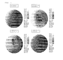
- Table 1 shows various conditions, an incidence of scratches and an incidence of SOI film thickness distribution abnormalities of Example 1 and Comparative Examples 1 to 6. Also, FIGS. 3 show measurement results of an SOI film thickness distribution of Example 1 and Comparative Examples 3 to 5.
- Table 1 EXAMPLE 1 COMPARATIVE EXAMPLE 1 COMPARATIVE EXAMPLE 2 COMPARATIVE EXAMPLE 3 COMPARATIVE EXAMPLE 4 COMPARATIVE EXAMPLE 5 COMPARATIVE EXAMPLE 6
- Example 1 having performed the inventive method in which the temperature-decreasing rate was less than 3.0°C/min and the take-out temperature was 250°C or less, the incidence of scratches was limited to a small value of 5%, and the incidence of SOI film thickness distribution abnormalities was suppressed to be 5%. In this way, an excellent SOI wafer free of scratches and SOI film thickness abnormalities could be manufactured at a good yield.
- a bond wafer consisting of a 300-mm-diameter silicon single crystal wafer both surfaces of which have been mirror-polished was thermally oxidized to form a 150-nm-thickness thermal oxide film on all surfaces thereof. Then, the bond wafer was immersed in HF aqueous solution while the back surface oxide film thereof was protected by an O-ring to remove the front surface oxide film. After that, the front surface was re-polished by CMP processing, and subjected to the thermal oxidation again to form a 30-nm-thickness thermal oxide film (for a buried oxide film) on the front surface side. At this time, the back surface oxide film grew to be 155nm.
- the resultant bond wafer was bonded to a base wafer consisting of a 300-mm-diameter silicon single crystal wafer.
- the delamination heat treatment was then performed (at 500°C, for 30min, in nitrogen atmosphere) to manufacture an SOI wafer, and subjected to an SC1 cleaning.
- the temperature-decreasing rate was set at 2.0°C/min and the take-out temperature inside the heat treatment furnace was set at 250°C.
- a bond wafer which has been delaminated by the ion implantation delamination method (a delaminated bond wafer having a 150-nm-thickness back surface oxide film) was immersed in HF aqueous solution while the back surface oxide film was protected by an O-ring to remove the front surface oxide film, and then subjected to the reclaiming process by CMP processing.
- the obtained wafer was used as a bond wafer, and thermally oxidized to form a 30-nm-thickness thermal oxide film (for a buried oxide film) on the front surface side. At this time, the back surface oxide film grew to be 155nm.
- the resultant bond wafer was bonded to a base wafer consisting of a 300-mm-diameter silicon single crystal wafer.
- the delamination heat treatment was then performed (at 500°C, for 30min, in nitrogen atmosphere) to manufacture an SOI wafer, and subjected to an SC1 cleaning.
- the temperature-decreasing rate was set at 2.0°C/min and the take-out temperature inside the heat treatment furnace was set at 250°C.
- a bond wafer consisting of a 300-mm-diameter silicon single crystal wafer both surfaces of which have been mirror-polished was thermally oxidized to form a 150-nm-thickness thermal oxide film on all surfaces thereof. Then, the bond wafer was immersed in HF aqueous solution while the back surface oxide film thereof was protected by an O-ring to remove the front surface oxide film. After that, the front surface was re-polished by CMP processing, and subjected to the thermal oxidation again to form a 30-nm-thickness thermal oxide film (for a buried oxide film) on the front surface side. At this time, the back surface oxide film grew to be 155nm.
- the resultant bond wafer was bonded to a base wafer consisting of a 300-mm-diameter silicon single crystal wafer.
- the delamination heat treatment was then performed (at 500°C, for 30min, in nitrogen atmosphere) to manufacture an SOI wafer, and subjected to an SC1 cleaning.
- the temperature-decreasing rate was set at 2.5°C/min and the take-out temperature inside the heat treatment furnace was set at 250°C.
- a 30-nm-thickness thermal oxide film was formed on a bond wafer consisting of a 300-mm-diameter silicon single crystal wafer both surfaces of which have been mirror-polished. Then, after hydrogen ions and helium ions were implanted through the 30-nm-thickness thermal oxide film, the resultant bond wafer was bonded to a base wafer consisting of a 300-mm-diameter silicon single crystal wafer. The delamination heat treatment was then performed (at 500°C, for 30min, in nitrogen atmosphere) to manufacture an SOI wafer, and subjected to an SC1 cleaning.
- the temperature-decreasing rate was set at 3.0°C/min and the take-out temperature inside the heat treatment furnace was set at 350°C.
- Table 2 shows various conditions, an incidence of scratches and an incidence of SOI film thickness distribution abnormalities of Examples 2 to 4 and Comparative Example 7.
- EXAMPLE 2 EXAMPLE 3
- EXAMPLE 4 COMPARATIVE EXAMPLE 7 THE NUMBER OF TIMES OF REUSE OF THE BOND WAFER 0 1 1 0 BACK SURFACE OXIDE FILM OF THE BOND WAFER 155nm 155nm 155nm 30nm FRONT SURFACE OXIDE FILM OF THE BOND WAFER (BURIED OXIDE FILM) 30nm 30nm 30nm 30nm 30nm 30nm 30nm 30nm 30nm H ION IMPLANTAION 30KeV, 5e16cm -2 30KeV, 5e16cm -2 30KeV, 1.5e16cm -2 30KeV, 1.5e16cm -2 He ION IMPLANTAION - - 50KeV, 1e16cm -2 50K
- Example 4 although the coimplantation was performed in the ion implantation, the above-explained excellent SOI wafer could be obtained unlike in the conventional manner.
- Comparative Example 7 in which the temperature-decreasing rate and the take-out temperature were different from those of the present invention, the incidence of scratches and the incidence of SOI film thickness distribution abnormalities were high values of 50% and 100%, respectively.
Landscapes
- Element Separation (AREA)
Abstract
Description
- The present invention relates to a method for manufacturing an SOI wafer by the ion implantation delamination method.
- In manufacture of an SOI wafer by the ion implantation delamination method, when a bond wafer for forming an SOI layer (Silicon On Insulator layer, or Semiconductor On Insulator in a broad sense) and a base wafer are bonded through an oxide film, and then subjected to a heat treatment (a delamination heat treatment) to perform a delamination at an ion-implanted layer, the wafers just after delamination are taken out from a heat treatment furnace with which the delamination heat treatment has been performed in a state that an SOI layer surface (a delaminating plane) of the SOI wafer faces to a surface (a delaminating plane) of the bond wafer (See
Patent Document 1, etc.). - When a bond wafer on which an oxide film has been formed and a base wafer are bonded to manufacture an SOI wafer, the SOI wafer warps in a convex shape on the delaminating plane side due to a buried oxide film which has been transferred from a surface of the bond wafer by the delamination heat treatment, whereas the bond wafer after delamination warps in a concave shape on the delaminating plane side in contrast to the SOI wafer because the front surface oxide film is separated and the oxide film remains only on the back surface. Although a magnitude of the warpage is determined depending on a thickness of the transferred oxide film, a contact between the SOI wafer and the bond wafer after delamination hardly occurs because magnitudes of the warpages of these wafers are almost the same.
- In practice, however, there is also the influence of a warp shape formed during wafer processing. Therefore, for example, if the bond wafer warps convexly during wafer processing, the bond wafer after delamination is formed into a shape obtained by subtracting the convex shape formed during the wafer processing from the concave shape due to the influence of the back surface oxide film.
- In this case, a mismatch in warp shape between the SOI wafer and the bond wafer after delamination is caused. More specifically, a magnitude of the concave warp of the bond wafer after delamination becomes small compared with a magnitude of the convex warp of the SOI wafer.
- In addition, in the ion implantation delamination method by the so-called coimplantation in which the ion implantation is performed by implanting two types of ion, for example, a hydrogen ion and a helium ion to form an ion-implanted layer at which delamination is caused, if the helium ion is implanted more deeply than the hydrogen ion, a helium ion-implanted layer remains in the bond wafer still after delamination while a hydrogen ion-implanted layer is divided into an SOI side and the bond wafer after delamination because the delamination is caused at the hydrogen ion-implanted layer. In this case, warping force by which the bond wafer after delamination is warped so as to have a convex shape operates on the bond wafer after delamination by existence of the helium ion-implanted layer, thereby causing the mismatch in warp shape with the SOI wafer.
- Patent Document 1:Japanese Unexamined Patent publication (Kokai) No.
2009-283582 - The present inventors keenly conducted studies the above-mentioned method for manufacturing an SOI wafer by the ion implantation delamination method, and consequently found that, in the manufactured SOI wafer, SOI film thickness abnormalities in which a portion having a thin SOI film thickness is generated at a center portion of the SOI wafer are caused, and scratches occur at the thin film portion as shown in
FIG. 4 . - The present invention was accomplished in view of the above-described problems. It is an object of the present invention to provide a method for manufacturing an SOI wafer that can inhibit scratches and SOI film thickness abnormalities.
- To achieve this object, the present invention provides a method for manufacturing an SOI wafer, comprising: implanting one or more gas ion selected from a hydrogen ion and a rare gas ion into a bond wafer composed of a semiconductor single crystal substrate from a surface of the bond wafer to form an ion-implanted layer; bonding the surface from which the ion is implanted into the bond wafer and a surface of a base wafer through an oxide film; and then delaminating the bond wafer at the ion-implanted layer by performing a delamination heat treatment with a heat treatment furnace to form the SOI wafer, wherein after the delamination heat treatment, a temperature of the heat treatment furnace is decreased to 250°C or less at temperature-decreasing rate of less than 3.0°C/min, and then the SOI wafer and the bond wafer after delamination are taken out from the heat treatment furnace.
- In the present invention, first of all, the temperature inside the heat treatment furnace during taking out the SOI wafer and the bond wafer of 250°C or less enables the formation of an oxide film during taking out the wafers to be inhibited. Even if a tip part of the convex shape of the SOI wafer is in contact with the bond wafer after delamination because of the mismatch, the occurrence of the conventional film thickness abnormalities at the tip part of the convex shape of the SOI wafer can be inhibited since the formation of the oxide film during taking out the wafers is inhibited on all surfaces of the wafer from the beginning.
- Moreover, in the present invention, the temperature-decreasing rate of less than 3.0°C/min enables a temperature distribution of the wafer surface to be small during decreasing the temperature, so that a deformation of the wafer due to the temperature distribution can be reduced. Therefore, the occurrence of scratches of the SOI wafer can be inhibited.
- Thus, the present invention enables an SOI wafer in which scratches and SOI film thickness abnormalities are inhibited to be obtained.
- In the method, a semiconductor single crystal substrate having a front surface oxide film and a back surface oxide film may be prepared as the bond wafer for forming the ion-implanted layer to implant the ion through the front surface oxide film, the back surface oxide film being thicker than the front surface oxide film.
- In this manner, the bond wafer after delamination is formed into a concave shape by a difference in film thickness among the oxide films, therefore the mismatch in warp shape between the SOI wafer and the bond wafer after delamination can be prevented, and the occurrence of scratches and SOI film thickness abnormalities due to the contact can be more greatly inhibited.
- Moreover, a wafer may be used as the semiconductor single crystal substrate having the back surface oxide film thicker than the front surface oxide film, the wafer being manufactured by forming a thermal oxide film on all surfaces of a semiconductor single crystal substrate, then removing a portion of the thermal oxide film on a front surface side to obtain a semiconductor single crystal substrate having the thermal oxide film only on a back surface side thereof, and thermally oxidizing the semiconductor single crystal substrate having the thermal oxide film only on the back surface side.
- In this manner, the difference in film thickness between the oxide film on the front surface that will become a surface to be bonded and the oxide film on the back surface can be appropriately adjusted.
- Moreover, before the semiconductor single crystal substrate having the thermal oxide film only on the back surface side is thermally oxidized, the front surface side on which the portion of the thermal oxide film has been removed may be polished.
- In this manner, failures during bonding can be inhibited.
- Moreover, a wafer manufactured by subjecting the bond wafer delaminated at the ion-implanted layer to a reclaiming process may be used as the semiconductor single crystal substrate having the back surface oxide film thicker than the front surface oxide film.
- In this manner, an SOI wafer can be manufactured economically.
- In the method, the reclaiming process may be performed without removing the back surface oxide film of the delaminated bond wafer.
- In this manner, it is easy to adjust the difference in film thickness among the oxide films of the bond wafer.
- Moreover, the ion implantation may be performed by a coimplantation of a hydrogen ion and a helium ion such that the helium ion is implanted more deeply than the hydrogen ion.
- The present invention can suppress the influence on warping of the bond wafer after delamination due to existence of the helium ion-implanted layer, and thereby prevent the mismatch in warp shape between the SOI wafer and the bond wafer after delamination, even if the helium ion is implanted more deeply than the hydrogen ion.
- As described above, the present invention can prevent the contact between the SOI wafer and the bond wafer after delamination due to the mismatch in relation to the delamination heat treatment in the ion implantation delamination method. In addition to this, a formation irregularity of the oxide film during taking out the wafers from the heat treatment furnace can be prevented even if the mismatch is caused. In this way, the occurrence of scratches and SOI film thickness abnormalities at the tip part of the convex shape of the SOI wafer can be inhibited.
-
-
FIG. 1 is a flow chart of an example of the inventive method for manufacturing an SOI wafer; -
FIG. 2 is a flow chart of an another example of the inventive method for manufacturing an SOI wafer; -
FIGS. 3 are diagrams showing measurement results of SOI film thickness distributions of Example 1 and Comparative examples 3 to 5; and -
FIG. 4 is a measurement diagram showing scratches and SOI film thickness abnormalities generated at a center portion of the SOI wafer. - Hereinafter, embodiments of the present invention will be described in detail with reference to the drawings, but the present invention is not limited thereto.
- The background of how the present inventors accomplished the present invention will now be described in detail.
- The present inventors found that, in the delamination heat treatment of the ion implantation delamination method for manufacturing an SOI wafer, if a magnitude of the concave shape of the bond wafer after delamination (the delaminated bond wafer) is smaller than that of the convex shape of the SOI wafer, a mismatch in warp shape is caused between the delaminated bond wafer and the SOI wafer, a tip part of the convex shape of the SOI layer surface is thereby brought into contact with the delaminated bond wafer in the delamination heat treatment process, and scratches and SOI film thickness abnormalities are likely to occur at a center portion of the SOI wafer and the like.
- In the case of bonding with the bond wafer on which a thermal oxide film has been formed, the SOI wafer warps convexly toward the delaminating plane side in proportion to the film thickness of the buried oxide film. On the other hand, in the delaminated bond wafer, the delaminating plane side warps concavely by action of the oxide film on the back surface because the oxide film on the front surface is separated by the delamination.
- As described above, a magnitude of the convex shape of the SOI wafer is usually equal to a magnitude of the concave shape of the delaminated bond wafer, so that the tip part of the convex shape of the SOI wafer is hardly in contact with the delaminated bond wafer.
- However, the above-mentioned mismatch possibly occurs, for example, by the influence of a warp shape formed in wafer processing.
- First, the present inventors investigated a mechanism of causing film thickness abnormalities.
- As a result, they found that the formation of an oxide film is inhibited at a contact portion in which the tip part of the convex shape of the SOI layer surface is in contact with the delaminated bond wafer, compared with a portion not in contact with the same. In this case, a thickness of the oxide film formed on the contact portion becomes thinner, and Si etching is started from the contact portion in SC1 cleaning of RCA cleaning (a cleaning with a mixed aqueous solution of NH4OH and H2O2) after delamination. Thus, it was revealed that the SOI film thickness of the tip part of the convex shape is reduced after cleaning.
- Then, a method is devised in which after the delamination heat treatment with a heat treatment furnace, the take-out temperature inside the heat treatment furnace is set at 250°C or less to inhibit the formation of an oxide film on the SOI wafer surface in order to improve non-uniformity in thickness of the oxide film to be formed on the SOI layer surface after delamination. If the wafers are taken out from the furnace at a temperature exceeded 250°C, an oxide film is formed on the SOI wafer surface by oxygen contained in air. Therefore, non-uniformity in oxide film thickness between the wafer contact portion and the noncontact portion is caused.
- The take-out temperature of 250°C or less can inhibit the oxide film from being formed on the surface during taking out the wafers from the beginning, thereby minimize an oxide film thickness distribution of the wafer surface. Si etching is therefore performed uniformly in a plane in the subsequent SC1 cleaning, and the occurrence of the conventional film thickness abnormalities can be inhibited.
- In addition, as for scratches, the temperature-decreasing rate of less than 3.0°C/min at which the temperature is decreased to the take-out temperature of 250°C or less after the SOI layer is delaminated in the delamination heat treatment (for example, at from 400 to 600°C) can minimize a temperature distribution of the wafer surface during decreasing the temperature, and inhibit scratching of the SOI wafer and the delaminated bond wafer due to a deformation of the wafer. If the temperature-decreasing rate is 3.0°C/min or more, a radial temperature distribution during decreasing the temperature is increased, and scratches easily occur because the wafer is deformed by a difference in thermal expansion coefficients.
- The present inventors found the foregoing, thereby brought the present invention to completion.
- Hereinafter, the inventive method for manufacturing an SOI wafer will be described in detail.
-
FIG. 1 shows an example of the inventive method for manufacturing an SOI wafer. - First, a semiconductor
single crystal substrate 2 is prepared as thebond wafer 1 to form an oxide film 3 (FIG. 1 at (A) ). - The semiconductor single crystal substrate used as the bond wafer is preferably a silicon single crystal wafer. In addition, a germanium single crystal wafer, a germanium epitaxial wafer, an SiGe epitaxial wafer, a strained silicon wafer or an SiC single crystal wafer can also be used alternatively. In this embodiment, the case of using a silicon single crystal wafer is described.
- Also, a method for forming the
oxide film 3 is not particularly limited to, the oxide film may be formed by thermal oxidation, for example. - Next, ions are implanted into the semiconductor
single crystal substrate 1 having theoxide film 3 formed thereon from a side to be bonded (a front surface side) to form an ion-implanted layer (FIG. 1 at (B) ). - The ion-implanted layer may be, for example, a layer formed by implanting one or more gas ion selected from a hydrogen ion and a rare gas ion. In this embodiment, the case of implanting hydrogen ions (a hydrogen ion-implanted layer 4) is described as an example.
- Subsequently, the surface from which the ions are implanted into the
bond wafer 1 and a surface of thebase wafer 5 are bonded through theoxide film 3, for example, at room temperature of from 20 to 30°C to form a bonded wafer 6 (FIG. 1 at (C) and (D) ). In this case, a plasma treatment may also be performed on a surface to be bonded of at least one of the bond wafer and the base wafer before bonding to increase the bonding strength obtained at room temperature. - Also, as the
base wafer 5, a silicon single crystal wafer or a silicon single crystal wafer on which an insulator film has been formed can be used, for example. - Then, the bonded
wafer 6 is loaded into a heat treatment furnace and heated, then the delamination heat treatment is performed at a prescribed temperature. The delamination heat treatment temperature may be, for example, 400°C or more, preferably from 400 to 600°C. The temperature in the above range enables the bondedwafer 6 to be appropriately delaminated at the hydrogen ion-implantedlayer 4, and thereby a delaminated bond wafer 1' and anSOI wafer 8 having anSOI layer 7 can be obtained (FIG. 1 at (E) ). - Here, a batch type furnace can be used as the heat treatment furnace, for example. This is not a limitation, provided the delamination heat treatment can be appropriately performed on wafers and a temperature inside the furnace can be decreased at a later-explained temperature-decreasing rate.
- After the delamination heat treatment is performed as described above, a temperature inside the heat treatment furnace is decreased at a rate of less than 3.0°C/min. The
SOI wafer 8 and the delaminated bond wafer 1' are then taken out under the temperature decreased to 250°C or less. - In this way, the decreasing of the temperature at the rate of less than 3.0°C/min can reduce a temperature distribution of each wafer surface during decreasing the temperature, and inhibit scratching of the
SOI wafer 8 and the delaminated bond wafer 1' due to a deformation of the wafer. Therefore, the occurrence of scratches can be prevented. - In addition, the temperature-decreasing rate is preferably 2.5°C/min or less. A lower limit thereof is not particularly limited to, but preferably 1.0°C/min or more to perform the heat treatment process efficiently.
- Moreover, the take-out temperature of 250°C or less can inhibit an oxide film from being formed on the surface during taking out the wafers. Therefore, even if a mismatch between the
SOI wafer 8 and the delaminated bond wafer 1' is caused, there is no possibility that the oxide film in a tip part of the convex shape of the SOI wafer is formed thinly than other portion unlike in the conventional manner, and a radial oxide film thickness distribution can be minimized. Therefore, a formation irregularity of the oxide film thickness can be inhibited, Si etching is uniformly performed in a radial direction by the subsequent step of SC1 cleaning, and the occurrence of the conventional film thickness abnormalities of the SOI wafer can be prevented. - In this way, the
SOI wafer 8 in which scratches are inhibited and the occurrence of SOI film thickness abnormalities is also inhibited can be obtained. - In the first embodiment, as the bond wafer, the case of using the semiconductor single crystal substrate in which a thermal oxide film is merely formed on all surfaces thereof has been described.
- However, in addition to this, the present invention can also use a semiconductor single crystal substrate having a back surface oxide film thicker than a front surface oxide film (an oxide film formed on the side to be bonded) as the bond wafer. This case is now described with reference to
FIG. 2 . - First, an oxide film 23' is formed on a back surface of a semiconductor single crystal substrate 22 (
FIG. 2 at (A) ). The oxide film 23' on the back surface is preferably a thermal oxide film, for example. A preferable method for forming the same is to manufacture a bond wafer having a thermal oxide film only on the back surface by forming a thermal oxide film on all surfaces of the bond wafer, and then removing a portion of the thermal oxide film on the side to be bonded of the bond wafer. - Other methods for forming the oxide film 23' on the back surface include a method in which after forming a thermal oxide film having almost uniform thickness on all surfaces of the semiconductor single crystal substrate, while a part of the oxide film on the back surface is protected by a ring-shaped rubber (O-ring) or a protective sheet such as PVC, the semiconductor single crystal substrate is brought into contact with an etching solution for oxide film, or a method in which a part of the thermal oxide film is removed on the side to be bonded with a solution containing hydrogen fluoride (HF) by a spin etching etc. to remain the oxide film only on the back surface.
- Next, another oxide film is formed on the semiconductor
single crystal substrate 22 having the oxide film 23' formed on the back surface (FIG. 2 at (B) ). Another oxide film is preferably a thermal oxide film. A preferable method for forming the same is to thermally oxidize all surfaces of the bond wafer having the back surface oxide film formed thereon. In this way, the wafer having theoxide film 23 in which the back surface side is thicker than the front surface side that will become the surface to be bonded of the semiconductorsingle crystal substrate 22 can be obtained. Thebond wafer 21 having an oxide film different in thickness in front and back is thus manufactured. - Also, if failures during bonding are caused by a deterioration in surface roughness of the surface to be bonded of the bond wafer or an attachment of a particle due to the formation of the oxide film on the back surface and the removing of the oxide film on the side to be bonded (the front surface side), the method may comprise a step of polishing the side to be bonded by using chemical mechanical polishing (CMP) etc. after removing the oxide film on the side to be bonded, and then thermal oxidation may be performed on all surfaces (
FIG. 2 between (A) and (B)). - As described above, the
bond wafer 21 in which the oxide film on the back surface is thicker than the oxide film on the front surface that will become the surface to be bonded can be previously formed into a concave shape before boding to the base wafer, and thereby the contact between the delaminated bond wafer and the SOI wafer can be inhibited. Moreover, this can inhibit the bond wafer from excessively warping and having a convex shape, thereby enabling the inhibition of the occurrence of the mismatch, even if a helium ion-implanted layer is formed as explained later. - In addition, a degree of how thickly the oxide film on the back surface is formed compared with the oxide film on the surface to be bonded can be appropriately determined by experiments and calculations based on specifications of the SOI wafer to be manufactured (such as diameter, base wafer thickness and BOX layer thickness) and specifications of the bond wafer to be used (such as diameter and wafer thickness) so as to prevent the mismatch just after delamination (so that a magnitude of the convex shape of the SOI wafer is equal to a magnitude of the concave shape of the delaminated bond wafer).
- Next, ions are implanted into the
bond wafer 21 having theoxide film 23 formed thereon from the side to be bonded (the front surface side) to form an ion-implanted layer. - In the first embodiment, the case of forming only the hydrogen ion-implanted layer has been described. Here, the case of forming a co-implanted layer by implanting both of hydrogen ions and helium ions will be described as an example.
- When a coimplantaion using hydrogen ions and helium ions is performed as the ion implantation, first, hydrogen ions are implanted to form a hydrogen ion-implanted layer 24 (
FIG. 2 at (C) ). Next, it is preferable that helium ions are implanted more deeply than the hydrogen ion-implantedlayer 24 to form a helium ion-implanted layer 24' (FIG. 2 at (D) ). The coimplantation thus performed can reduce an amount of ions to be implanted compared with the case of implanting one type of ions. - In the conventional method for manufacturing an SOI wafer, if hydrogen ions and helium ions are co-implanted, the delaminated bond wafer is formed into convex shape by existence of the helium ion-implanted layer, so that the mismatch in warp shape with the SOI wafer occurs, resulting in scratches and SOI film thickness abnormalities.
- However, as shown in
FIG. 2 at (B) , the thick thickness of the oxide film on the back surface enables the warp shape of the bond wafer to be previously adjusted before bonding, thereby the influence by existence of the helium ion-implanted layer 24' can be minimized. - Next, the surface from which the ions are implanted into the
bond wafer 21 and a surface of thebase wafer 25 are bonded through theoxide film 23, for example, at room temperature of from 20 to 30°C to form a bonded wafer 26 (FIG. 2 at (E) and (F) ). - Then, the bond wafer is delaminated from the bonded
wafer 26 at the hydrogen ion-implantedlayer 24 by the delamination heat treatment so as to obtain a delaminated bond wafer 21', and thereby forming anSOI wafer 28 having an SOI layer 27 (FIG. 2 at (G) ). The delamination heat treatment conditions may be set, for example, as in the first embodiment. - In the second embodiment, since the bond wafer having the oxide film in which the back surface side is thicker than the front surface side is used, the delaminated bond wafer 21' warps in a concave shape more reliably, and the conventional contact due to the mismatch in shape between the delaminated bond wafer and the SOI wafer can be prevented.
- Therefore, an SOI wafer in which scratches and SOI film thickness abnormalities after Si etching are further inhibited can be obtained more stably.
- In addition, the method for manufacturing an SOI wafer by the ion implantation delamination method is also characterize by being capable of reusing a delaminated bond wafer. Therefore, the present invention can also use a wafer manufactured by subjecting the delaminated bond wafer 21' and the like to a reclaiming process as the bond wafer. Thus, it is advantageous in a cost.
- In that case, the delaminated bond wafer is reclaimed by performing the reclaiming process without removing the oxide film on the back surface to manufacture a bond wafer having an oxide film on the back surface. The resultant wafer is then thermally oxidized, and thereby the bond wafer in which the oxide film on the back surface is thicker than the oxide film on the surface to be bonded can be easily manufactured.
- In this reclaiming process of the delaminated bond wafer, a removal of the oxide film remaining on an outer circumferential unbonded portion on the side to be bonded may be accomplished by directly polishing the side to be bonded. Alternatively, the removal may be performed using a method in which the delaminated bond wafer is brought into contact with an etching solution for oxide film while a part of the oxide film on the back surface is protected by a ring-shaped rubber (O-ring) or a protective sheet such as PVC, or using a spin etching machine.
- In the reclaiming process of the delaminated bond wafer, the back surface oxide film may be protected by blocking an etching solution or an etching gas by means of an O-ring, or by attaching a protective sheet, such as PVC, to the back surface of the delaminated bond wafer, as described above. A possible alternative way is performed such that an etching solution or an etching gas does not reach the back surface of the bond wafer because of wind pressure and centrifugal force generated by the rotation of the wafer. The etching solution for oxide film is preferably a HF solution. Alternatively, the etching may be performed with a HF gas. The O-ring is desirably provided at a position several millimeters from the outer circumference to warp the bond wafer. Depending on a permissible level of warping, however, it may be provided within the inside of this range.
- By subjecting the bond wafer having the back surface oxide film thicker than the front surface oxide film that is thus manufactured by reclaiming the delaminated bond wafer, to the steps of (C) to (G) in
FIG. 2 as in the second embodiment, for example, an SOI wafer in which scratches and SOI film thickness abnormalities after Si etching are further inhibited can be obtained. - Hereinafter, the present invention will be more specifically described with reference to examples and comparative examples, but the present invention is not limited thereto.
- A bond wafer consisting of a 300-mm-diameter silicon single crystal wafer both surfaces of which have been mirror-polished was thermally oxidized to form a 30-nm-thickness thermal oxide film on all surfaces thereof, and subjected to the hydrogen ion-implantation though the thermal oxide film. Subsequently, the resultant bond wafer was bonded to a base wafer consisting of a 300-mm-diameter silicon single crystal wafer to manufacture a bonded wafer. The delamination heat treatment was then performed (at 500°C, for 30min, in nitrogen atmosphere) to delaminate a part of the bond wafer from the bonded wafer so that an SOI wafer was manufactured, and subjected to an SC1 cleaning.
- In addition, the temperature-decreasing rate and the take-out temperature inside the heat treatment furnace were set as follows.
Example 1 Temperature-decreasing rate: 2.0°C/min, Take-out temperature: 250°C;
Comparative Example 1 Temperature-decreasing rate: 3.0°C/min, Take-out temperature: 250°C;
Comparative Example 2 Temperature-decreasing rate: 3.0°C/min, Take-out temperature: 225°C;
Comparative Example 3 Temperature-decreasing rate: 3.0°C/min, Take-out temperature: 500°C;
Comparative Example 4 Temperature-decreasing rate: 3.0°C/min, Take-out temperature: 360°C;
Comparative Example 5 Temperature-decreasing rate: 3.0°C/min, Take-out temperature: 295°C;
Comparative Example 6 Temperature-decreasing rate: 5.0°C/min, Take-out temperature: 250°C; - Table 1 shows various conditions, an incidence of scratches and an incidence of SOI film thickness distribution abnormalities of Example 1 and Comparative Examples 1 to 6. Also,
FIGS. 3 show measurement results of an SOI film thickness distribution of Example 1 and Comparative Examples 3 to 5.(Table 1) EXAMPLE 1 COMPARATIVE EXAMPLE 1 COMPARATIVE EXAMPLE 2 COMPARATIVE EXAMPLE 3 COMPARATIVE EXAMPLE 4 COMPARATIVE EXAMPLE 5 COMPARATIVE EXAMPLE 6 BACK SURFACE OXIDE FILM OF THE BOND WAFER 30nm 30nm 30nm 30nm 30nm 30nm 30nm FRONT SURFACE OXIDE FILM OF THE BOND WAFER (BURIED OXIDE FILM) 30nm 30nm 30nm 30nm 30nm 30nm 30nm H ION IMPLANTAION 30KeV, 5e16cm-2 30KeV, 5e16cm-2 30KeV, 5e16cm-2 30KeV, 5e16cm-2 30KeV, 5e16cm-2 30KeV, 5e16cm-2 30KeV, 5e16cm-2 BONDING PROCESS BONDING AT ROOM TEMPERATURE BONDING AT ROOM TEMPERATURE BONDING AT ROOM TEMPERATURE BONDING AT ROOM TEMPERATURE BONDING AT ROOM TEMPERATURE BONDING AT ROOM TEMPERATURE BONDING AT ROOM TEMPERATURE DELAMINATION HEAT TREATMENT 500°C, 30min 500°C, 30min 500°C, 30min 500°C, 30min 500°C, 30min 500°C, 30min 500°C, 30min TEMPERATURE-DECREASING RATE 2.0°C/min 3.0°C/min 3.0°C/min 3.0°C/min 3.0°C/min 3.0°C/min 5.0°C/min TAKE-OUT TEMPERATURE 250°C 250°C 225°C 500°C 360°C 295°C 250°C INCIDENCE OF SCRATCHES 5% 10% 10% 100% 50% 30% 20% INCIDENCE OF SOI FILM THICKNESS DISTRIBUTION ABNORMALITIES 5% 5% 5% 100% 100% 50% 40% - As shown in Table 1 and
FIGS. 3 , in Example 1 having performed the inventive method in which the temperature-decreasing rate was less than 3.0°C/min and the take-out temperature was 250°C or less, the incidence of scratches was limited to a small value of 5%, and the incidence of SOI film thickness distribution abnormalities was suppressed to be 5%. In this way, an excellent SOI wafer free of scratches and SOI film thickness abnormalities could be manufactured at a good yield. - By contrast, in Comparative Examples 1 to 5 in which the temperature-decreasing rate was 3.0°C/min as in the conventional method, the incidence of scratches was 10%, 10%, 100%, 50% and 30%, respectively. These values were from 2 to 20 times that of Example 1.
- Moreover, the incidence of scratches was 20% in Comparative Example 6 in which the temperature-decreasing rate was 5.0°C/min and other conditions were the same as in Example 1 (2.0°C/min) and Comparative Example 1 (3.0°C/min). This result was worse than Example 1 and Comparative Example 1.
- Moreover, in Comparative Examples 3 to 5 in which the take-out temperature was more than 250°C unlike the present invention, the incidence of SOI film thickness distribution abnormalities was a high value of 100%, 100% and 50%, respectively.
- A bond wafer consisting of a 300-mm-diameter silicon single crystal wafer both surfaces of which have been mirror-polished was thermally oxidized to form a 150-nm-thickness thermal oxide film on all surfaces thereof. Then, the bond wafer was immersed in HF aqueous solution while the back surface oxide film thereof was protected by an O-ring to remove the front surface oxide film. After that, the front surface was re-polished by CMP processing, and subjected to the thermal oxidation again to form a 30-nm-thickness thermal oxide film (for a buried oxide film) on the front surface side. At this time, the back surface oxide film grew to be 155nm. After hydrogen ions were implanted through the 30-nm-thickness thermal oxide film on the front surface side, the resultant bond wafer was bonded to a base wafer consisting of a 300-mm-diameter silicon single crystal wafer. The delamination heat treatment was then performed (at 500°C, for 30min, in nitrogen atmosphere) to manufacture an SOI wafer, and subjected to an SC1 cleaning.
- In addition, the temperature-decreasing rate was set at 2.0°C/min and the take-out temperature inside the heat treatment furnace was set at 250°C.
- A bond wafer which has been delaminated by the ion implantation delamination method (a delaminated bond wafer having a 150-nm-thickness back surface oxide film) was immersed in HF aqueous solution while the back surface oxide film was protected by an O-ring to remove the front surface oxide film, and then subjected to the reclaiming process by CMP processing. The obtained wafer was used as a bond wafer, and thermally oxidized to form a 30-nm-thickness thermal oxide film (for a buried oxide film) on the front surface side. At this time, the back surface oxide film grew to be 155nm. After hydrogen ions were implanted through the 30-nm-thickness thermal oxide film on the front surface side, the resultant bond wafer was bonded to a base wafer consisting of a 300-mm-diameter silicon single crystal wafer. The delamination heat treatment was then performed (at 500°C, for 30min, in nitrogen atmosphere) to manufacture an SOI wafer, and subjected to an SC1 cleaning.
- In addition, the temperature-decreasing rate was set at 2.0°C/min and the take-out temperature inside the heat treatment furnace was set at 250°C.
- A bond wafer consisting of a 300-mm-diameter silicon single crystal wafer both surfaces of which have been mirror-polished was thermally oxidized to form a 150-nm-thickness thermal oxide film on all surfaces thereof. Then, the bond wafer was immersed in HF aqueous solution while the back surface oxide film thereof was protected by an O-ring to remove the front surface oxide film. After that, the front surface was re-polished by CMP processing, and subjected to the thermal oxidation again to form a 30-nm-thickness thermal oxide film (for a buried oxide film) on the front surface side. At this time, the back surface oxide film grew to be 155nm. After hydrogen ions and helium ions were implanted through the 30-nm-thickness thermal oxide film, the resultant bond wafer was bonded to a base wafer consisting of a 300-mm-diameter silicon single crystal wafer. The delamination heat treatment was then performed (at 500°C, for 30min, in nitrogen atmosphere) to manufacture an SOI wafer, and subjected to an SC1 cleaning.
- In addition, the temperature-decreasing rate was set at 2.5°C/min and the take-out temperature inside the heat treatment furnace was set at 250°C.
- A 30-nm-thickness thermal oxide film was formed on a bond wafer consisting of a 300-mm-diameter silicon single crystal wafer both surfaces of which have been mirror-polished. Then, after hydrogen ions and helium ions were implanted through the 30-nm-thickness thermal oxide film, the resultant bond wafer was bonded to a base wafer consisting of a 300-mm-diameter silicon single crystal wafer. The delamination heat treatment was then performed (at 500°C, for 30min, in nitrogen atmosphere) to manufacture an SOI wafer, and subjected to an SC1 cleaning.
- In addition, the temperature-decreasing rate was set at 3.0°C/min and the take-out temperature inside the heat treatment furnace was set at 350°C.
- Table 2 shows various conditions, an incidence of scratches and an incidence of SOI film thickness distribution abnormalities of Examples 2 to 4 and Comparative Example 7.
(Table 2) EXAMPLE 2 EXAMPLE 3 EXAMPLE 4 COMPARATIVE EXAMPLE 7 THE NUMBER OF TIMES OF REUSE OF THE BOND WAFER 0 1 1 0 BACK SURFACE OXIDE FILM OF THE BOND WAFER 155nm 155nm 155nm 30nm FRONT SURFACE OXIDE FILM OF THE BOND WAFER (BURIED OXIDE FILM) 30nm 30nm 30nm 30nm H ION IMPLANTAION 30KeV, 5e16cm-2 30KeV, 5e16cm-2 30KeV, 1.5e16cm-2 30KeV, 1.5e16cm-2 He ION IMPLANTAION - - 50KeV, 1e16cm-2 50KeV, 1e16cm-2 BONDING PROCESS BONDING AT ROOM TEMPERATURE BONDING AT ROOM TEMPERATURE BONDING AT ROOM TEMPERATURE BONDING AT ROOM TEMPERATURE DELAMINATION HEAT TREATMENT 500°C, 30min 500°C, 30min 500°C, 30min 500°C, 30min TEMPERATURE-DECREASING RATE 2.0°C/min 2.0°C/min 2.5°C/min 3.0°C/min TAKE-OUT TEMPERATURE 250°C 250°C 250°C 350°C INCIDENCE OF SCRATCHES 0% 0% 0% 50% INCIDENCE OF SOI FILM THICKNESS DISTRIBUTION ABNORMALITIES 0% 0% 0% 100% - As shown in Table 2, in Examples 2 to 4 in which a silicon single crystal wafer having the back surface oxide film thicker than the front surface oxide film was used as the bond wafer according to the present invention, both the incidence of scratches and the incidence of SOI film thickness distribution abnormalities were 0%, and an excellent SOI wafer could be manufactured.
- Moreover, in Example 4, although the coimplantation was performed in the ion implantation, the above-explained excellent SOI wafer could be obtained unlike in the conventional manner.
- On the other hand, in Comparative Example 7 in which the temperature-decreasing rate and the take-out temperature were different from those of the present invention, the incidence of scratches and the incidence of SOI film thickness distribution abnormalities were high values of 50% and 100%, respectively.
- It is to be noted that the present invention is not limited to the foregoing embodiment. The embodiment is just an exemplification, and any examples that have substantially the same feature and demonstrate the same functions and effects as those in the technical concept described in claims of the present invention are included in the technical scope of the present invention.
Claims (7)
- A method for manufacturing an SOI wafer, comprising:implanting one or more gas ion selected from a hydrogen ion and a rare gas ion into a bond wafer composed of a semiconductor single crystal substrate from a surface of the bond wafer to form an ion-implanted layer;bonding the surface from which the ion is implanted into the bond wafer and a surface of a base wafer through an oxide film; and thendelaminating the bond wafer at the ion-implanted layer by performing a delamination heat treatment with a heat treatment furnace to form the SOI wafer, wherein after the delamination heat treatment, a temperature of the heat treatment furnace is decreased to 250°C or less at temperature-decreasing rate of less than 3.0°C/min, and then the SOI wafer and the bond wafer after delamination are taken out from the heat treatment furnace.
- The method for manufacturing an SOI wafer according to claim 1, wherein a semiconductor single crystal substrate having a front surface oxide film and a back surface oxide film is prepared as the bond wafer for forming the ion-implanted layer to implant the ion through the front surface oxide film, the back surface oxide film being thicker than the front surface oxide film.
- The method for manufacturing an SOI wafer according to claim 2, wherein a wafer is used as the semiconductor single crystal substrate having the back surface oxide film thicker than the front surface oxide film, the wafer being manufactured by forming a thermal oxide film on all surfaces of a semiconductor single crystal substrate, then removing a portion of the thermal oxide film on a front surface side to obtain a semiconductor single crystal substrate having the thermal oxide film only on a back surface side thereof, and thermally oxidizing the semiconductor single crystal substrate having the thermal oxide film only on the back surface side.
- The method for manufacturing an SOI wafer according to claim 3, wherein before the semiconductor single crystal substrate having the thermal oxide film only on the back surface side is thermally oxidized, the front surface side on which the portion of the thermal oxide film has been removed is polished.
- The method for manufacturing an SOI wafer according to any one of claims 2 to 4, wherein a wafer manufactured by subjecting the bond wafer delaminated at the ion-implanted layer to a reclaiming process is used as the semiconductor single crystal substrate having the back surface oxide film thicker than the front surface oxide film.
- The method for manufacturing an SOI wafer according to claim 5, wherein thereclaiming process is performed without removing the back surface oxide film of the delaminated bond wafer.
- The method for manufacturing an SOI wafer according to any one of claims 1 to 6, wherein the ion implantation is performed by a coimplantation of a hydrogen ion and a helium ion such that the helium ion is implanted more deeply than the hydrogen ion.
Applications Claiming Priority (2)
| Application Number | Priority Date | Filing Date | Title |
|---|---|---|---|
| JP2012274110A JP5780234B2 (en) | 2012-12-14 | 2012-12-14 | Manufacturing method of SOI wafer |
| PCT/JP2013/006560 WO2014091670A1 (en) | 2012-12-14 | 2013-11-07 | Soi wafer manufacturing method |
Publications (3)
| Publication Number | Publication Date |
|---|---|
| EP2887383A1 true EP2887383A1 (en) | 2015-06-24 |
| EP2887383A4 EP2887383A4 (en) | 2016-03-30 |
| EP2887383B1 EP2887383B1 (en) | 2020-03-25 |
Family
ID=50933979
Family Applications (1)
| Application Number | Title | Priority Date | Filing Date |
|---|---|---|---|
| EP13863262.5A Active EP2887383B1 (en) | 2012-12-14 | 2013-11-07 | Soi wafer manufacturing method |
Country Status (7)
| Country | Link |
|---|---|
| US (1) | US9337080B2 (en) |
| EP (1) | EP2887383B1 (en) |
| JP (1) | JP5780234B2 (en) |
| KR (1) | KR101901872B1 (en) |
| CN (1) | CN104885190B (en) |
| SG (1) | SG11201502119TA (en) |
| WO (1) | WO2014091670A1 (en) |
Families Citing this family (9)
| Publication number | Priority date | Publication date | Assignee | Title |
|---|---|---|---|---|
| JP6437404B2 (en) * | 2015-09-09 | 2018-12-12 | 東芝メモリ株式会社 | Manufacturing method of semiconductor device |
| CN105702564B (en) * | 2016-03-29 | 2018-10-16 | 上海华力微电子有限公司 | A method of improving silicon wafer warpage degree |
| US20180033609A1 (en) * | 2016-07-28 | 2018-02-01 | QMAT, Inc. | Removal of non-cleaved/non-transferred material from donor substrate |
| US20180019169A1 (en) * | 2016-07-12 | 2018-01-18 | QMAT, Inc. | Backing substrate stabilizing donor substrate for implant or reclamation |
| CN106597583B (en) * | 2016-12-30 | 2019-01-18 | 上海集成电路研发中心有限公司 | A kind of structures and methods forming optical spectroscopic lens |
| FR3061988B1 (en) * | 2017-01-13 | 2019-11-01 | Soitec | SURFACE MELTING METHOD OF SEMICONDUCTOR SUBSTRATE ON INSULATION |
| FR3064398B1 (en) | 2017-03-21 | 2019-06-07 | Soitec | SEMICONDUCTOR TYPE STRUCTURE ON INSULATION, ESPECIALLY FOR A FRONT-SIDE TYPE IMAGE SENSOR, AND METHOD FOR MANUFACTURING SUCH STRUCTURE |
| CN113921389B (en) * | 2021-10-08 | 2025-02-07 | 长鑫存储技术有限公司 | Leveling method and semiconductor structure |
| US20250232977A1 (en) * | 2024-01-12 | 2025-07-17 | Ii-Vi Delaware, Inc. | Implantation process to mitigate bowing of wafers introduced by splitting process |
Family Cites Families (16)
| Publication number | Priority date | Publication date | Assignee | Title |
|---|---|---|---|---|
| JPH098124A (en) * | 1995-06-15 | 1997-01-10 | Nippondenso Co Ltd | Insulation separation substrate and manufacturing method thereof |
| JP3395661B2 (en) * | 1998-07-07 | 2003-04-14 | 信越半導体株式会社 | Method for manufacturing SOI wafer |
| JP2002110688A (en) * | 2000-09-29 | 2002-04-12 | Canon Inc | SOI heat treatment method and manufacturing method |
| JP2003347176A (en) * | 2002-03-20 | 2003-12-05 | Shin Etsu Handotai Co Ltd | Manufacturing method of bonded wafer |
| JP4407127B2 (en) | 2003-01-10 | 2010-02-03 | 信越半導体株式会社 | Manufacturing method of SOI wafer |
| US20070069335A1 (en) * | 2003-09-08 | 2007-03-29 | Akihiko Endo | Bonded wafer and its manufacturing method |
| JP4398934B2 (en) * | 2005-02-28 | 2010-01-13 | 信越半導体株式会社 | Manufacturing method of SOI wafer |
| CN101124657B (en) * | 2005-02-28 | 2010-04-14 | 信越半导体股份有限公司 | Bonded wafer manufacturing method and bonded wafer |
| US20100112814A1 (en) | 2006-09-06 | 2010-05-06 | Sowmya Krishnan | Pre-certified process chamber and method |
| JP5183969B2 (en) * | 2007-05-29 | 2013-04-17 | 信越半導体株式会社 | Method for forming silicon oxide film on SOI wafer |
| US7763502B2 (en) * | 2007-06-22 | 2010-07-27 | Semiconductor Energy Laboratory Co., Ltd | Semiconductor substrate, method for manufacturing semiconductor substrate, semiconductor device, and electronic device |
| JP2009283582A (en) | 2008-05-21 | 2009-12-03 | Shin Etsu Handotai Co Ltd | Bonded wafer manufacturing method and bonded wafer |
| JP5548395B2 (en) | 2008-06-25 | 2014-07-16 | 株式会社半導体エネルギー研究所 | Method for manufacturing SOI substrate |
| US8148237B2 (en) * | 2009-08-07 | 2012-04-03 | Varian Semiconductor Equipment Associates, Inc. | Pressurized treatment of substrates to enhance cleaving process |
| US20130089968A1 (en) * | 2010-06-30 | 2013-04-11 | Alex Usenko | Method for finishing silicon on insulator substrates |
| JP5479304B2 (en) * | 2010-11-10 | 2014-04-23 | 信越半導体株式会社 | Method for forming thermal oxide film on silicon single crystal wafer |
-
2012
- 2012-12-14 JP JP2012274110A patent/JP5780234B2/en active Active
-
2013
- 2013-11-07 CN CN201380064933.0A patent/CN104885190B/en active Active
- 2013-11-07 WO PCT/JP2013/006560 patent/WO2014091670A1/en not_active Ceased
- 2013-11-07 EP EP13863262.5A patent/EP2887383B1/en active Active
- 2013-11-07 KR KR1020157015578A patent/KR101901872B1/en active Active
- 2013-11-07 US US14/428,700 patent/US9337080B2/en active Active
- 2013-11-07 SG SG11201502119TA patent/SG11201502119TA/en unknown
Also Published As
| Publication number | Publication date |
|---|---|
| JP5780234B2 (en) | 2015-09-16 |
| EP2887383A4 (en) | 2016-03-30 |
| US20150249035A1 (en) | 2015-09-03 |
| US9337080B2 (en) | 2016-05-10 |
| KR101901872B1 (en) | 2018-09-28 |
| EP2887383B1 (en) | 2020-03-25 |
| KR20150093703A (en) | 2015-08-18 |
| CN104885190B (en) | 2018-01-02 |
| CN104885190A (en) | 2015-09-02 |
| JP2014120587A (en) | 2014-06-30 |
| SG11201502119TA (en) | 2015-05-28 |
| WO2014091670A1 (en) | 2014-06-19 |
Similar Documents
| Publication | Publication Date | Title |
|---|---|---|
| EP2887383B1 (en) | Soi wafer manufacturing method | |
| US9773694B2 (en) | Method for manufacturing bonded wafer | |
| EP2924736B1 (en) | Method for manufacturing soi wafer | |
| KR101066315B1 (en) | Manufacturing method of bonded wafer | |
| EP3309820B1 (en) | Method of manufacturing soi wafer | |
| EP3118889B1 (en) | Process for producing bonded soi wafer | |
| US20180122639A1 (en) | Method for manufacturing bonded soi wafer | |
| EP2579296A1 (en) | Method for manufacturing bonded wafer | |
| EP3522202B1 (en) | Bonded soi wafer manufacturing method | |
| KR20150070096A (en) | Soi wafer manufacturing method | |
| JP5564785B2 (en) | Manufacturing method of bonded substrate | |
| WO2014080565A1 (en) | Soi wafer manufacturing method | |
| JP2005079389A (en) | Method and board for separating laminated wafer | |
| WO2017217129A1 (en) | Bonded wafer manufacturing method | |
| KR20160052551A (en) | Bonded wafer manufacturing method | |
| JP2006013179A (en) | Method for manufacturing soi wafer |
Legal Events
| Date | Code | Title | Description |
|---|---|---|---|
| PUAI | Public reference made under article 153(3) epc to a published international application that has entered the european phase |
Free format text: ORIGINAL CODE: 0009012 |
|
| 17P | Request for examination filed |
Effective date: 20150318 |
|
| AK | Designated contracting states |
Kind code of ref document: A1 Designated state(s): AL AT BE BG CH CY CZ DE DK EE ES FI FR GB GR HR HU IE IS IT LI LT LU LV MC MK MT NL NO PL PT RO RS SE SI SK SM TR |
|
| AX | Request for extension of the european patent |
Extension state: BA ME |
|
| RAP1 | Party data changed (applicant data changed or rights of an application transferred) |
Owner name: SHIN-ETSU HANDOTAI CO., LTD. |
|
| DAX | Request for extension of the european patent (deleted) | ||
| RA4 | Supplementary search report drawn up and despatched (corrected) |
Effective date: 20160226 |
|
| RIC1 | Information provided on ipc code assigned before grant |
Ipc: H01L 21/265 20060101ALI20160222BHEP Ipc: H01L 21/02 20060101AFI20160222BHEP Ipc: H01L 21/762 20060101ALI20160222BHEP Ipc: H01L 27/12 20060101ALI20160222BHEP |
|
| STAA | Information on the status of an ep patent application or granted ep patent |
Free format text: STATUS: EXAMINATION IS IN PROGRESS |
|
| 17Q | First examination report despatched |
Effective date: 20181025 |
|
| GRAP | Despatch of communication of intention to grant a patent |
Free format text: ORIGINAL CODE: EPIDOSNIGR1 |
|
| STAA | Information on the status of an ep patent application or granted ep patent |
Free format text: STATUS: GRANT OF PATENT IS INTENDED |
|
| INTG | Intention to grant announced |
Effective date: 20191017 |
|
| GRAS | Grant fee paid |
Free format text: ORIGINAL CODE: EPIDOSNIGR3 |
|
| GRAA | (expected) grant |
Free format text: ORIGINAL CODE: 0009210 |
|
| STAA | Information on the status of an ep patent application or granted ep patent |
Free format text: STATUS: THE PATENT HAS BEEN GRANTED |
|
| AK | Designated contracting states |
Kind code of ref document: B1 Designated state(s): AL AT BE BG CH CY CZ DE DK EE ES FI FR GB GR HR HU IE IS IT LI LT LU LV MC MK MT NL NO PL PT RO RS SE SI SK SM TR |
|
| REG | Reference to a national code |
Ref country code: GB Ref legal event code: FG4D |
|
| RIN1 | Information on inventor provided before grant (corrected) |
Inventor name: ISHIZUKA, TORU Inventor name: YOKOKAWA, ISAO Inventor name: AGA, HIROJI |
|
| REG | Reference to a national code |
Ref country code: AT Ref legal event code: REF Ref document number: 1249547 Country of ref document: AT Kind code of ref document: T Effective date: 20200415 Ref country code: IE Ref legal event code: FG4D |
|
| REG | Reference to a national code |
Ref country code: DE Ref legal event code: R096 Ref document number: 602013067287 Country of ref document: DE |
|
| PG25 | Lapsed in a contracting state [announced via postgrant information from national office to epo] |
Ref country code: FI Free format text: LAPSE BECAUSE OF FAILURE TO SUBMIT A TRANSLATION OF THE DESCRIPTION OR TO PAY THE FEE WITHIN THE PRESCRIBED TIME-LIMIT Effective date: 20200325 Ref country code: NO Free format text: LAPSE BECAUSE OF FAILURE TO SUBMIT A TRANSLATION OF THE DESCRIPTION OR TO PAY THE FEE WITHIN THE PRESCRIBED TIME-LIMIT Effective date: 20200625 Ref country code: RS Free format text: LAPSE BECAUSE OF FAILURE TO SUBMIT A TRANSLATION OF THE DESCRIPTION OR TO PAY THE FEE WITHIN THE PRESCRIBED TIME-LIMIT Effective date: 20200325 |
|
| PG25 | Lapsed in a contracting state [announced via postgrant information from national office to epo] |
Ref country code: SE Free format text: LAPSE BECAUSE OF FAILURE TO SUBMIT A TRANSLATION OF THE DESCRIPTION OR TO PAY THE FEE WITHIN THE PRESCRIBED TIME-LIMIT Effective date: 20200325 Ref country code: LV Free format text: LAPSE BECAUSE OF FAILURE TO SUBMIT A TRANSLATION OF THE DESCRIPTION OR TO PAY THE FEE WITHIN THE PRESCRIBED TIME-LIMIT Effective date: 20200325 Ref country code: HR Free format text: LAPSE BECAUSE OF FAILURE TO SUBMIT A TRANSLATION OF THE DESCRIPTION OR TO PAY THE FEE WITHIN THE PRESCRIBED TIME-LIMIT Effective date: 20200325 Ref country code: GR Free format text: LAPSE BECAUSE OF FAILURE TO SUBMIT A TRANSLATION OF THE DESCRIPTION OR TO PAY THE FEE WITHIN THE PRESCRIBED TIME-LIMIT Effective date: 20200626 Ref country code: BG Free format text: LAPSE BECAUSE OF FAILURE TO SUBMIT A TRANSLATION OF THE DESCRIPTION OR TO PAY THE FEE WITHIN THE PRESCRIBED TIME-LIMIT Effective date: 20200625 |
|
| REG | Reference to a national code |
Ref country code: NL Ref legal event code: MP Effective date: 20200325 |
|
| REG | Reference to a national code |
Ref country code: LT Ref legal event code: MG4D |
|
| PG25 | Lapsed in a contracting state [announced via postgrant information from national office to epo] |
Ref country code: NL Free format text: LAPSE BECAUSE OF FAILURE TO SUBMIT A TRANSLATION OF THE DESCRIPTION OR TO PAY THE FEE WITHIN THE PRESCRIBED TIME-LIMIT Effective date: 20200325 |
|
| PG25 | Lapsed in a contracting state [announced via postgrant information from national office to epo] |
Ref country code: SM Free format text: LAPSE BECAUSE OF FAILURE TO SUBMIT A TRANSLATION OF THE DESCRIPTION OR TO PAY THE FEE WITHIN THE PRESCRIBED TIME-LIMIT Effective date: 20200325 Ref country code: LT Free format text: LAPSE BECAUSE OF FAILURE TO SUBMIT A TRANSLATION OF THE DESCRIPTION OR TO PAY THE FEE WITHIN THE PRESCRIBED TIME-LIMIT Effective date: 20200325 Ref country code: EE Free format text: LAPSE BECAUSE OF FAILURE TO SUBMIT A TRANSLATION OF THE DESCRIPTION OR TO PAY THE FEE WITHIN THE PRESCRIBED TIME-LIMIT Effective date: 20200325 Ref country code: RO Free format text: LAPSE BECAUSE OF FAILURE TO SUBMIT A TRANSLATION OF THE DESCRIPTION OR TO PAY THE FEE WITHIN THE PRESCRIBED TIME-LIMIT Effective date: 20200325 Ref country code: PT Free format text: LAPSE BECAUSE OF FAILURE TO SUBMIT A TRANSLATION OF THE DESCRIPTION OR TO PAY THE FEE WITHIN THE PRESCRIBED TIME-LIMIT Effective date: 20200818 Ref country code: CZ Free format text: LAPSE BECAUSE OF FAILURE TO SUBMIT A TRANSLATION OF THE DESCRIPTION OR TO PAY THE FEE WITHIN THE PRESCRIBED TIME-LIMIT Effective date: 20200325 Ref country code: IS Free format text: LAPSE BECAUSE OF FAILURE TO SUBMIT A TRANSLATION OF THE DESCRIPTION OR TO PAY THE FEE WITHIN THE PRESCRIBED TIME-LIMIT Effective date: 20200725 Ref country code: SK Free format text: LAPSE BECAUSE OF FAILURE TO SUBMIT A TRANSLATION OF THE DESCRIPTION OR TO PAY THE FEE WITHIN THE PRESCRIBED TIME-LIMIT Effective date: 20200325 |
|
| REG | Reference to a national code |
Ref country code: AT Ref legal event code: MK05 Ref document number: 1249547 Country of ref document: AT Kind code of ref document: T Effective date: 20200325 |
|
| REG | Reference to a national code |
Ref country code: DE Ref legal event code: R097 Ref document number: 602013067287 Country of ref document: DE |
|
| PG25 | Lapsed in a contracting state [announced via postgrant information from national office to epo] |
Ref country code: ES Free format text: LAPSE BECAUSE OF FAILURE TO SUBMIT A TRANSLATION OF THE DESCRIPTION OR TO PAY THE FEE WITHIN THE PRESCRIBED TIME-LIMIT Effective date: 20200325 Ref country code: AT Free format text: LAPSE BECAUSE OF FAILURE TO SUBMIT A TRANSLATION OF THE DESCRIPTION OR TO PAY THE FEE WITHIN THE PRESCRIBED TIME-LIMIT Effective date: 20200325 Ref country code: IT Free format text: LAPSE BECAUSE OF FAILURE TO SUBMIT A TRANSLATION OF THE DESCRIPTION OR TO PAY THE FEE WITHIN THE PRESCRIBED TIME-LIMIT Effective date: 20200325 Ref country code: DK Free format text: LAPSE BECAUSE OF FAILURE TO SUBMIT A TRANSLATION OF THE DESCRIPTION OR TO PAY THE FEE WITHIN THE PRESCRIBED TIME-LIMIT Effective date: 20200325 |
|
| PLBE | No opposition filed within time limit |
Free format text: ORIGINAL CODE: 0009261 |
|
| STAA | Information on the status of an ep patent application or granted ep patent |
Free format text: STATUS: NO OPPOSITION FILED WITHIN TIME LIMIT |
|
| PG25 | Lapsed in a contracting state [announced via postgrant information from national office to epo] |
Ref country code: PL Free format text: LAPSE BECAUSE OF FAILURE TO SUBMIT A TRANSLATION OF THE DESCRIPTION OR TO PAY THE FEE WITHIN THE PRESCRIBED TIME-LIMIT Effective date: 20200325 |
|
| 26N | No opposition filed |
Effective date: 20210112 |
|
| PG25 | Lapsed in a contracting state [announced via postgrant information from national office to epo] |
Ref country code: SI Free format text: LAPSE BECAUSE OF FAILURE TO SUBMIT A TRANSLATION OF THE DESCRIPTION OR TO PAY THE FEE WITHIN THE PRESCRIBED TIME-LIMIT Effective date: 20200325 |
|
| PG25 | Lapsed in a contracting state [announced via postgrant information from national office to epo] |
Ref country code: MC Free format text: LAPSE BECAUSE OF FAILURE TO SUBMIT A TRANSLATION OF THE DESCRIPTION OR TO PAY THE FEE WITHIN THE PRESCRIBED TIME-LIMIT Effective date: 20200325 |
|
| REG | Reference to a national code |
Ref country code: CH Ref legal event code: PL |
|
| GBPC | Gb: european patent ceased through non-payment of renewal fee |
Effective date: 20201107 |
|
| PG25 | Lapsed in a contracting state [announced via postgrant information from national office to epo] |
Ref country code: LU Free format text: LAPSE BECAUSE OF NON-PAYMENT OF DUE FEES Effective date: 20201107 |
|
| REG | Reference to a national code |
Ref country code: BE Ref legal event code: MM Effective date: 20201130 |
|
| PG25 | Lapsed in a contracting state [announced via postgrant information from national office to epo] |
Ref country code: LI Free format text: LAPSE BECAUSE OF NON-PAYMENT OF DUE FEES Effective date: 20201130 Ref country code: CH Free format text: LAPSE BECAUSE OF NON-PAYMENT OF DUE FEES Effective date: 20201130 |
|
| PG25 | Lapsed in a contracting state [announced via postgrant information from national office to epo] |
Ref country code: IE Free format text: LAPSE BECAUSE OF NON-PAYMENT OF DUE FEES Effective date: 20201107 |
|
| PG25 | Lapsed in a contracting state [announced via postgrant information from national office to epo] |
Ref country code: GB Free format text: LAPSE BECAUSE OF NON-PAYMENT OF DUE FEES Effective date: 20201107 |
|
| PG25 | Lapsed in a contracting state [announced via postgrant information from national office to epo] |
Ref country code: TR Free format text: LAPSE BECAUSE OF FAILURE TO SUBMIT A TRANSLATION OF THE DESCRIPTION OR TO PAY THE FEE WITHIN THE PRESCRIBED TIME-LIMIT Effective date: 20200325 Ref country code: MT Free format text: LAPSE BECAUSE OF FAILURE TO SUBMIT A TRANSLATION OF THE DESCRIPTION OR TO PAY THE FEE WITHIN THE PRESCRIBED TIME-LIMIT Effective date: 20200325 Ref country code: CY Free format text: LAPSE BECAUSE OF FAILURE TO SUBMIT A TRANSLATION OF THE DESCRIPTION OR TO PAY THE FEE WITHIN THE PRESCRIBED TIME-LIMIT Effective date: 20200325 |
|
| PG25 | Lapsed in a contracting state [announced via postgrant information from national office to epo] |
Ref country code: MK Free format text: LAPSE BECAUSE OF FAILURE TO SUBMIT A TRANSLATION OF THE DESCRIPTION OR TO PAY THE FEE WITHIN THE PRESCRIBED TIME-LIMIT Effective date: 20200325 Ref country code: AL Free format text: LAPSE BECAUSE OF FAILURE TO SUBMIT A TRANSLATION OF THE DESCRIPTION OR TO PAY THE FEE WITHIN THE PRESCRIBED TIME-LIMIT Effective date: 20200325 |
|
| PG25 | Lapsed in a contracting state [announced via postgrant information from national office to epo] |
Ref country code: BE Free format text: LAPSE BECAUSE OF NON-PAYMENT OF DUE FEES Effective date: 20201130 |
|
| PG25 | Lapsed in a contracting state [announced via postgrant information from national office to epo] |
Ref country code: IS Free format text: LAPSE BECAUSE OF NON-PAYMENT OF DUE FEES Effective date: 20200725 |
|
| REG | Reference to a national code |
Ref country code: DE Ref legal event code: R079 Ref document number: 602013067287 Country of ref document: DE Free format text: PREVIOUS MAIN CLASS: H01L0021020000 Ipc: H10P0095000000 |
|
| PGFP | Annual fee paid to national office [announced via postgrant information from national office to epo] |
Ref country code: DE Payment date: 20251119 Year of fee payment: 13 |
|
| PGFP | Annual fee paid to national office [announced via postgrant information from national office to epo] |
Ref country code: FR Payment date: 20251125 Year of fee payment: 13 |