EP2887120A1 - Améliorations portant sur ou en relation avec des guides d'onde - Google Patents
Améliorations portant sur ou en relation avec des guides d'onde Download PDFInfo
- Publication number
- EP2887120A1 EP2887120A1 EP13275324.5A EP13275324A EP2887120A1 EP 2887120 A1 EP2887120 A1 EP 2887120A1 EP 13275324 A EP13275324 A EP 13275324A EP 2887120 A1 EP2887120 A1 EP 2887120A1
- Authority
- EP
- European Patent Office
- Prior art keywords
- grating
- diffraction grating
- input
- output
- waveguide
- Prior art date
- Legal status (The legal status is an assumption and is not a legal conclusion. Google has not performed a legal analysis and makes no representation as to the accuracy of the status listed.)
- Ceased
Links
Images


Classifications
-
- G—PHYSICS
- G02—OPTICS
- G02B—OPTICAL ELEMENTS, SYSTEMS OR APPARATUS
- G02B6/00—Light guides; Structural details of arrangements comprising light guides and other optical elements, e.g. couplings
- G02B6/24—Coupling light guides
- G02B6/26—Optical coupling means
- G02B6/34—Optical coupling means utilising prism or grating
-
- G—PHYSICS
- G02—OPTICS
- G02B—OPTICAL ELEMENTS, SYSTEMS OR APPARATUS
- G02B27/00—Optical systems or apparatus not provided for by any of the groups G02B1/00 - G02B26/00, G02B30/00
- G02B27/0081—Optical systems or apparatus not provided for by any of the groups G02B1/00 - G02B26/00, G02B30/00 with means for altering, e.g. enlarging, the entrance or exit pupil
-
- G—PHYSICS
- G02—OPTICS
- G02B—OPTICAL ELEMENTS, SYSTEMS OR APPARATUS
- G02B5/00—Optical elements other than lenses
- G02B5/18—Diffraction gratings
- G02B5/1814—Diffraction gratings structurally combined with one or more further optical elements, e.g. lenses, mirrors, prisms or other diffraction gratings
- G02B5/1819—Plural gratings positioned on the same surface, e.g. array of gratings
- G02B5/1823—Plural gratings positioned on the same surface, e.g. array of gratings in an overlapping or superposed manner
Definitions
- the invention relates to a waveguide such as, but without limitation to, an optical waveguide for displays, and to a display device.
- the invention is relevant to a display device in which image-bearing light is injected into a waveguide, is expanded to form a visible image and is released from the waveguide for viewing.
- Prior art display devices of this type can comprise a slab waveguide containing three separate diffraction gratings arranged to perform a respective one of three successive functions.
- a first grating serves as a light input area for diffracting received light in a direction along the slab waveguide.
- a second grating serves to expand the light from the first grating in a first dimension, and a third grating serves to receive the expanded light and further expand the light in a second dimension orthogonal to the first dimension and to output the result from the waveguide.
- the second diffraction grating is able to diffract received light in a direction required to enable that diffracted light to reach the third diffraction grating, it is also necessary that the light is received by the second grating from the first grating in an appropriate direction relative to the orientation of the grating lines of the second grating.
- a misalignment between the orientation of grating lines in the first (input) grating and the second grating will result in a misalignment of light output from the second grating relative to the orientation of the grating lines of the third (output) grating.
- some prior art methods include pressing or stamping both the first and second gratings as different parts of one general grating structure having one common orientation of grating lines throughout. This may be in the form of two separated grating areas stamped from a common single grating stamper (e.g. Fig. 1A ) or in the form of two separate regions of one grating pattern stamped from one stamper (e.g. Fig.1B ).
- the second grating or grating region may receive the input light from the first grating or grating region at an appropriate angle of direction of incidence to the grating lines of the second grating for onward diffraction to the third (output) grating
- the light emanating from the first grating or grating region must be re-directed by being reflected back towards the second grating or grating region.
- a highly reflective surface must be provided along parts of an edge of the slab waveguide in order to achieve this.
- the reflective surface must be manufactured to a very high optical standard if it is to be of use. Polishing of a reflective slab edge to a very flat surface is required. This is difficult to achieve and such waveguides are expensive to produce.
- the present invention aims to address these matters.
- the invention provides a waveguide for a display apparatus comprising: a planar optical waveguide part for guiding light to be displayed; an input diffraction grating arranged to receive light and diffract the received light along the optical waveguide part for guiding thereby; an intermediate diffraction grating optically coupled to the input diffraction grating via the optical waveguide part and arranged to receive diffracted light from the input diffraction grating and to expand the received light in a first dimension by diffraction; an output diffraction grating optically coupled to the intermediate diffraction grating via the optical waveguide part and arranged to receive the expanded light and to output the received expanded light from the optical waveguide part by diffraction for display; wherein the input diffraction grating is positioned so as to be located wholly within the geographical area, or footprint, of the intermediate grating, and wherein the grating vectors of the input diffraction grating and the intermediate diffraction grat
- the projections of the grating vectors of the input diffraction grating and the intermediate diffraction grating onto the plane of the optical waveguide part may be oriented in different respective directions.
- the input diffraction grating may be positioned substantially in-plane or coplanar with the intermediate diffraction grating such that the physical location of the input diffraction grating is wholly within the geographical area or footprint of the intermediate diffraction grating.
- the input diffraction grating may be positioned adjacent to the intermediate diffraction grating (e.g. parallel to, but out-of-plane) such that the apparent location of the input diffraction grating is wholly within the geographical area or footprint of the intermediate diffraction grating.
- the location of the input diffraction grating as being wholly within the geographical area, or footprint, of the intermediate diffraction grating may be a physical/actual location or may be an apparent location.
- the apparent location of the input grating within that geographical area or footprint may be achieved by positioning the input grating suitably near to the intermediate diffraction grating such that a surface upon which the intermediate grating is formed, and which is enclosed by the outer bounds/periphery of the intermediate diffraction grating, extends wholly over the input grating, which is itself formed upon a separate surface.
- An example is to form the intermediate diffraction grating upon one planar surface of the optical waveguide part and to form the input diffraction grating upon the opposite planar surface of the waveguide part within the footprint of the intermediate grating as projected onto the latter planar surface (e.g. visible through the waveguide part).
- the material of the intermediate diffraction grating covers all of those parts of the surface of the optical waveguide part at one side thereof via which the received light is guided by total internal reflection from the input diffraction grating to the intermediate diffraction grating.
- the material of the intermediate diffraction grating is preferably continuous with the material of at least the input diffraction grating.
- the material of the intermediate diffraction grating may be continuous with the material of the output diffraction grating.
- the intermediate diffraction grating may be a surface relief grating formed in a surface of the waveguide.
- the input diffraction grating and the output diffraction grating may each be a relief grating formed in a surface of the waveguide.
- the intermediate diffraction grating may comprise a square-wave grating structure.
- the input grating or / and the output grating may comprise a blazed grating structure.
- the waveguide may include a coating upon the intermediate diffraction grating.
- the coating may have a refractive index which differs from the refractive index of the material of the intermediate diffraction grating.
- the waveguide may include a coating upon the input or / and the output diffraction grating, which may have a refractive index which differs from the refractive index of the material of the input or / and the output diffraction grating.
- the output diffraction grating is preferably arranged to receive the expanded light from the intermediate diffraction grating and to expand the received light in a second dimension transverse to the first dimension.
- the invention may provide a display device comprising the waveguide described above.
- the invention provides a method for manufacturing a waveguide for a display apparatus the waveguide including an input diffraction grating to receive light and diffract the received light along the waveguide, an intermediate diffraction grating to receive diffracted light from the input diffraction grating and to expand the received light in a first dimension by diffraction, and an output diffraction grating to receive and output the expanded light from the optical waveguide by diffraction, the method comprising: providing a planar optical waveguide part; depositing upon the optical waveguide part a fluid material curable to form an optically transparent solid; impressing upon the fluid material an impression defining an input diffraction grating region, an intermediate diffraction grating region and an output diffraction grating region wherein the fluid material of the intermediate diffraction grating region is continuous with the fluid material of at least the input diffraction grating region; curing the impressed fluid material to solidify the impression; wherein the input dif
- the projections of the grating vectors of the input diffraction grating and the intermediate diffraction grating onto the plane of the optical waveguide part are preferably oriented in different respective directions.
- the input diffraction grating may be positioned substantially in-plane or coplanar with the intermediate diffraction grating such that the physical location of the input diffraction grating is wholly within the geographical area or footprint of the intermediate diffraction grating.
- the cured material covers all of those parts of the surface of the optical waveguide part at one side thereof via which the received light is guided by total internal reflection from the input diffraction grating to the intermediate diffraction grating.
- the impressing may include impressing upon the fluid material at the same one side of the planar waveguide both the input grating and the intermediate diffraction grating.
- the impressing may include impressing upon the fluid material at the same one side of the planar waveguide both the input grating and the intermediate diffraction grating as a diffractive region surrounding the input grating.
- the fluid material of the intermediate diffraction grating region may be continuous with the fluid material of the output diffraction grating region.
- the impressing may include impressing upon the fluid material at the same one side of the planar waveguide each of the input grating, the intermediate diffraction and the output diffraction grating.
- the impressing may include impressing upon the fluid material simultaneously each of the input grating, the intermediate diffraction and the output diffraction grating.
- the curing may include curing the fluid material simultaneously for each of the input grating and the intermediate diffraction or additionally the output diffraction grating.
- the impressing may include impressing the intermediate diffraction grating with a square-wave grating structure.
- the impressing may include impressing the input grating or / and the output grating with a blazed grating structure.
- the method may include applying a coating upon the intermediate diffraction grating having a refractive index which differs from the refractive index of the material of the intermediate diffraction grating.
- the method may include applying a coating upon the input or / and the output diffraction grating having a refractive index which differs from the refractive index of the material of the input or / and the output diffraction grating.
- the output diffraction grating is preferably arranged to receive the expanded light from the intermediate diffraction grating and to expand the received light in a second dimension transverse to the first dimension.
- the invention may provide a method for manufacturing a waveguide for a display apparatus the waveguide including an input diffraction grating to receive light and diffract the received light along the waveguide, an intermediate diffraction grating to receive diffracted light from the input diffraction grating and to expand the received light in a first dimension by diffraction, and an output diffraction grating to receive and output the expanded light from the optical waveguide by diffraction, the method comprising: providing a planar optical waveguide part; depositing upon opposite planar surfaces of the optical waveguide part a fluid material curable to form an optically transparent solid; impressing upon the fluid material an impression defining an input diffraction grating, an intermediate diffraction grating, and an output diffraction grating; curing the impressed fluid material to solidify the impressions; wherein the input diffraction grating is positioned adjacent to the intermediate diffraction grating such that the apparent location of the input diffraction
- the projections of the grating vectors of the input diffraction grating and the intermediate diffraction grating onto the plane of the optical waveguide part are preferably oriented in different respective directions.
- the input diffraction grating may be positioned adjacent to the intermediate diffraction grating parallel to it, but out-of-plane from it, such that the apparent location of the input diffraction grating is wholly within the geographical area or footprint of the intermediate diffraction grating.
- the location of the input diffraction grating as being wholly within the geographical area, or footprint, of the intermediate diffraction grating may be an apparent location.
- the apparent location of the input grating within that geographical area or footprint may be achieved by positioning the input grating suitably near to the intermediate diffraction grating such that a surface upon which the intermediate grating is formed, and which is enclosed by the outer bounds/periphery of the intermediate diffraction grating, extends wholly over the input grating, which is itself formed upon a separate surface.
- An example is to form the intermediate diffraction grating upon one planar surface of the optical waveguide part and to form the input diffraction grating upon the opposite planar surface of the waveguide part within the footprint of the intermediate grating as projected onto the latter planar surface (e.g. visible through the waveguide part).
- the fluid material is preferably deposited upon each of two opposite sides of the planar waveguide part, and the impressing preferably includes impressing upon the fluid material at one side of the planar waveguide the intermediate diffraction grating as a diffractive region surrounding a substantially non-diffractive input window region, and impressing upon the fluid material at the opposite side of the planar waveguide the input grating such that the input grating is visible through the input window region.
- the cured material covers all of those parts of the surface of the optical waveguide part at one side thereof via which the received light is guided by total internal reflection from the input diffraction grating to the intermediate diffraction grating.
- the fluid material of the intermediate diffraction grating region may be continuous with the fluid material of the output diffraction grating region.
- the impressing may include impressing upon the fluid material at the same one side of the planar waveguide each of the intermediate diffraction gating and the output diffraction grating.
- the curing may include curing simultaneously the fluid material each of the intermediate diffraction grating and the output diffraction grating at the one side of the planar waveguide, and subsequently applying the fluid material at the opposite side of the planar waveguide.
- the impressing may include subsequently impressing the input grating upon the fluid material at the opposite side of the planar waveguide.
- the method may include adjusting the orientation of the input diffraction grating impressed into the fluid material relative to the solidified intermediate diffraction grating and solidified output diffraction grating, and subsequently curing the impressed input diffraction grating at a chosen orientation.
- the impressing may include impressing the intermediate diffraction grating with a square-wave grating structure.
- the impressing may include impressing the input grating or / and the output grating with a blazed grating structure.
- the method may include applying a coating upon the intermediate diffraction grating having a refractive index which differs from the refractive index of the material of the intermediate diffraction grating.
- the method may include applying a coating upon the input or / and the output diffraction grating having a refractive index which differs from the refractive index of the material of the input or / and the output diffraction grating.
- the output diffraction grating is preferably arranged to receive the expanded light from the intermediate diffraction grating and to expand the received light in a second dimension transverse to the first dimension.
- Figure 1A shows a prior art waveguide for a display apparatus.
- the waveguide comprises a slab optical waveguide 1 for guiding light internally by total internal reflection between two opposing parallel and planar surfaces of the slab.
- Image-bearing light to be displayed is input to the slab via an input diffraction grating 2 arranged to receive the image-bearing light 6 and to diffract the received light 7 along the slab optical waveguide for guiding across an intermediate diffraction grating 4 optically coupled to the input diffraction grating.
- the intermediate grating 4 is arranged to expand the received light in a first dimension 7 by diffraction and to direct the expanded light 8 towards an output diffraction grating 5 optically coupled to the intermediate diffraction grating via the slab optical waveguide.
- the output grating is arranged to receive the expanded light 8 from the and to output 9 the received expanded light from the slab optical waveguide by diffraction for display to a user 10.
- the input diffraction grating 2 is optically coupled to the intermediate diffraction grating via a reflective edge part of the slab waveguide which is coated by a reflective coating 3. Accordingly, input light 6 is diffracted towards the reflective edge and is guided to that reflective coating/edge 3 by total internal reflection within the slab waveguide. Upon reflection at the reflective edge, the guided input light is guided thereafter towards the intermediate diffraction grating 4.
- Figure 1 B schematically illustrates a prior art variant of the prior art device of Figure 1A in which the input diffraction grating 2 is structured as a contiguous grating region connected to the intermediate diffraction grating by being integrally formed with, and joined to, the intermediate grating region.
- the form and operation of the apparatus of Figure 1B is otherwise identical to that of the apparatus of Figure 1A , and light rays (6, 7, 8 and 9) are indicated in Figure 1B to illustrate this.
- the grating lines of the input diffraction grating ( Fig.1A ) or input diffraction grating region ( Fig.1B ) are substantially parallel to the grating lines of the intermediate diffraction grating, or grating region (their grating vectors are identical), and so requires the use of a reflective edge 3 to redirect the input light 7 into the appropriate direction relative to the grating lines of the intermediate grating.
- the commonly oriented grating lines (grating vectors) of the input and intermediate gratings (or grating regions) of both examples of prior art devices are produced by use of a single grating stamper bearing such commonly oriented grating lines/grooves in relief as is now described in relation to the apparatus of Fig.1A . It is to be noted that this production method applies equally to the manufacture of the device of Fig.1B . In both cases, the projection of the grating vectors of the input and intermediate grating parts onto the planar surface of the waveguide substrate are substantially parallel simply because those vectors are the same.
- FIGS 2A to 2F schematically illustrate the manufacturing process in question.
- the process begins ( Fig.2A ) with the depositing upon a slab optical waveguide substrate 1 of a fluid curing glue 11 which is curable to form an optically transparent solid. Three separate, discrete and isolated deposits of curing glue are deposited upon the substrate at locations where it is intended to form three separate diffraction grating regions coupled optically to each other by the waveguide substrate.
- a grating stamper 12 is introduced to the process.
- the grating stamper bears upon one surface three surface relief patters (13, 14, 15) each one of which represents a respective one of three separate surface relief diffraction gratings.
- Each surface relief pattern of the grating stamper is in negative, or reciprocal, form to the grating it is designed to stamp.
- the relief of grating lines 13 for the input grating are substantially parallel to the relief pattern of grating lines 14 for the intermediate grating.
- the grating stamper is impressed upon the three discrete deposits of fluid curing glue, in unison, to form an impression upon those three deposits corresponding to a respective one of three separate and discrete diffraction gratings.
- the three diffraction gratings define an input diffraction grating region defined by a first surface relief pattern 13 of the grating stamper, an intermediate diffraction grating region defined by a second surface relief pattern 14 of the grating stamper and an output diffraction grating region defined by a third surface relief pattern 15 of the grating stamper.
- the same basic process is applied in manufacturing the apparatus of Fig.1B with the modification that the grating stamper comprises two separate surface relief patterns in which one pattern corresponds to the combined input and intermediate grating structure and the other corresponds to the output grating structure. Also, only two discrete deposits of fluid curing glue are required - one for the combined gratings and one for the output grating.
- the multi-coloured light is output from the waveguide substrate 1. Any angular misalignment between the direction of output of the light of different colours is observed. Such a misalignment would be due to a misalignment between the reflective edge 3 of the waveguide substrate and the input diffraction grating pattern impressed by the first surface relief grating pattern 13 of the grating stamper and the intermediate diffraction grating pattern 14 impressed by the grating stamper since the grating grooves of those two patterns are substantially parallel. In effect, the angle of incidence of input light from the former must be accurately aligned such that light is coupled to the subsequent diffraction gratings optimally.
- the next manufacturing step ( Fig.2D ) requires careful rotation of the grating stamper relative to the waveguide substrate (and its reflective edge 3) to re-align the fluid diffraction grating impressions within the curing glue deposits.
- Optimal alignment is detected when angular alignment if the different colours of output light beams is observed.
- the fluid curing glue is subsequently cured ( Fig.2E ) by irradiating it with ultraviolet (UV) radiation.
- UV ultraviolet
- the resulting waveguide 1 is parted from the waveguide stamper 12 ( Fig.2F ) and includes in surface relief an input diffraction grating 2 to receive light and diffract the received light along the waveguide towards the reflective edge 3, an intermediate diffraction grating 4 to receive diffracted light from the reflective edge 3 and to expand the received light in a first dimension by diffraction, and an output diffraction grating 5 to receive and output the expanded light from the optical waveguide by diffraction.
- Two embodiments of the invention each provide a waveguide for a display apparatus which address these problems of manufacture and product.
- the embodiments each comprise a slab optical waveguide substrate (20, 24) for guiding light to be displayed.
- the substrate bears an input diffraction grating (21, 28) arranged upon a surface to receive image-bearing light and diffract the received light along the optical waveguide directly towards an intermediate grating 25 so that the light is guided within the waveguide.
- An intermediate diffraction grating (22, 25) is formed on a surface of the waveguide and is optically coupled to the input diffraction grating (20, 24) via the optical waveguide. It is arranged to receive diffracted light from the input diffraction grating directly and to expand the received light in a first dimension by diffraction.
- the grating lines/grooves of the input grating are not parallel to those of the intermediate grating such that the grating vectors of the two gratings have different orientations, as do their respective projections onto the planar surface of the waveguide substrate.
- the grating vectors lie parallel to the plane of the waveguide structure and, as such, their respective projections thereupon are equal to the vectors themselves.
- the input grating is located within the geographical area, or footprint, of the intermediate grating.
- the actual location of the input grating may be defined as within the bounds of the intermediate grating (e.g. Fig.3 ) or that the apparent location of the input grating may be defined as within the bounds of the intermediate grating (e.g. Fig.4 ).
- An output diffraction grating (23, 27) is optically coupled to the intermediate diffraction grating via the optical waveguide part and is arranged to receive the expanded light and to output the received expanded light from the optical waveguide, by diffraction, for display.
- the material of the intermediate diffraction grating (22, 25) covers all of those parts of the surface of the optical waveguide part, at one side of the waveguide slab, via which the input image-bearing light is guided by total internal reflection from the input diffraction grating (21, 28) to the intermediate diffraction grating (22, 25).
- the material of the intermediate diffraction grating 22 is continuous with the material of the input diffraction grating 21.
- the material of the input diffraction grating 28 is not continuous with the material of the intermediate grating 25.
- the intermediate grating 25 and the output grating 27 of this alternative embodiment are each formed on a first planar side 24A of the slab waveguide substrate opposite to the second planar side 24B of the slab waveguide substrate upon which the input grating 28 is formed.
- Figure 4 shows both the first and second slab sides bearing these three diffraction gratings (dashed arrows point to gratings seen "through" the waveguide slab).
- the intermediate diffraction grating on one side 24A of the waveguide substrate comprises as a diffractive region 25 surrounding a circular and substantially non-diffractive input window region 26.
- the opposite side 24B of the planar waveguide substrate bears the input grating 28 positioned in register with the input window region 26 such that the input grating is visible through the input window region.
- the input window region may comprise the same material of, and be continuous with, the material of the surrounding diffractive region 25 forming the intermediate diffraction grating.
- the input window region may be defined by the absence of material leaving bare and exposed a region of the slab waveguide substrate exposed and un-covered/coated.
- the apparent location of the input diffraction grating 28, apparent through the input window 26, is within the bounds of the intermediate grating and as such is located within the geographical area or footprint of the intermediate grating.
- the actual location of the input diffraction grating 21 is within the bounds of the intermediate grating.
- the input grating is out-of-plane with the intermediate grating, and in the latter case it is in-plane.
- the material of the intermediate diffraction grating (22, 25) may also be continuous with the material of the output diffraction grating (23, 27) in one or each of these embodiments.
- the output diffraction grating may be formed in-plane with the intermediate grating and/or the input grating or out-of-plane with either/both. This may be achieved by forming the output grating on an appropriate one of the two opposite surfaces of the waveguide substrate.
- the intermediate diffraction grating (22, 25) is a square-wave surface relief grating formed in a surface of cured curing glue deposited upon a surface of the slab waveguide substrate (20, 24).
- both the input diffraction grating (21, 28) and the output diffraction grating (23, 27) are each a blazed surface relief grating formed in a surface of cured curing glue deposited on a surface of the slab waveguide substrate.
- a dielectric or metallic coating may be deposited upon the input, intermediate and / or output diffraction gratings as desired.
- the coating preferably has a refractive index which differs from (e.g. is greater than) the refractive index of the material of the cured curing glue forming the coated diffraction grating in question.
- a waveguide is for use in a display device comprising the waveguide described above.
- Examples include a helmet-mounted head-up display (HUD), or a HUD for mounting in a vehicle (e.g. cockpit, cabin etc. of a tactical vehicle or other vehicle).
- HUD helmet-mounted head-up display
- vehicle e.g. cockpit, cabin etc. of a tactical vehicle or other vehicle.
- Figure 5 schematically shows the waveguide of either of the embodiments of Figure 3 or Figure 4 , in use.
- Image-bearing light 6 to be displayed is input to the slab waveguide (20, 24A) at the input diffraction grating (21, 28), whereupon it is diffracted and guided 7 along the slab optical waveguide directly towards and across the intermediate diffraction grating (22, 25) by virtue of the non-parallel selected orientation of its grating lines/grooves (or grating vector) relative to the grating lines/grooves (or grating vector) of the intermediate grating.
- the intermediate grating is arranged to expand the received light in a first dimension 7 by diffraction and to direct the expanded light 8, by virtue of the orientation of its grating lines/grooves (or grating vector) towards the output diffraction grating (23, 27) via the slab optical waveguide, for output 9, and viewing by a user 10.
- the output grating is arranged to receive the expanded light 8 from the intermediate grating (22, 25) and to output 9 the received expanded light from the slab optical waveguide by diffraction for display.
- the orientation of the grating lines/grooves (i.e. grating vector) of the output grating differs from that of the grating lines/grooves (grating vector) of the intermediate grating.
- Figure 5 shows the input diffraction grating located within the intermediate diffraction grating and formed in common with differently-oriented grating lines/grooves/vector (as in Fig.3 ) or formed separately but visible through the input window region of the waveguide (as in Fig.4 ) as appropriate to the embodiment concerned.
- Figures 6 , 7 , 8 and 9 illustrated advantageous aspects of the invention as compared to prior art waveguides such as illustrated in Figure 1A or 1B .
- this reduction in width / area of the intermediate grating means that light which has been diffracted by the intermediate diffraction grating in a direction towards the output grating (i.e. "turned” towards the output grating) is required to pass along less area of intermediate diffraction grating in its path towards the output grating.
- TIR total internal reflection
- Figures 8 and 9 illustrate a further advantage of preferred embodiments of the invention in which the material of the intermediate diffraction grating covers all of those parts of the surface of the optical waveguide part at one side thereof via which the received image-bearing light is guided by total internal reflection from the input diffraction grating to the intermediate diffraction grating.
- the input grating and intermediate grating are continuous (in-plane) on the same one side of the waveguide substrate.
- Figure 4 when the input grating is replaced by an input window 26 continuous with the intermediate grating which comprises the same material as the material of the intermediate grating.
- the input grating in that case is visible on the reverse side of the slab waveguide substrate through the input window.
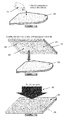
- Figure 8 shows a side-by-side comparison of a section through the input grating and intermediate grating of a hypothetical comparative waveguide (lefthand image) and a waveguide according to an embodiment of the invention (right-hand image). It can be seen that the effect of producing isolated and discrete input and output diffraction gratings upon the waveguide substrate surface is to present a structural edge to the path of guided light within the waveguide substrate, at which scattering of light can occur. This results in the loss of light which reduces image brightness, and also the contamination of image-bearing light with random scattered light which degrades the output image contrast and resolution.
- Figure 9 illustrates this effect in an exploded view of parts of the sectional view of the hypothetical waveguide of Figure 8 .
- the material of the intermediate diffraction grating covers all of those parts of the upper surface of the optical waveguide part at the one side thereof (bearing the intermediate grating and, in a continuum of material, either the material of the input grating or the material of the input window), there is no such scattering edge presented to the guided light passing to the intermediate grating by total internal reflection.
- FIGS 10A to 10D schematically illustrate the manufacturing process by which the waveguide of Figure 3 may be manufactured.
- the process begins ( Fig.10A ) with the depositing upon a slab optical waveguide substrate 20 a fluid curing glue 11 which is curable to form an optically transparent solid. Two separate, discrete and isolated deposits of curing glue are deposited upon the substrate at locations where it is intended to form two separate diffraction grating regions coupled optically to each other by the waveguide substrate.
- a grating stamper 30 is introduced to the process.
- the grating stamper bears upon one surface three surface relief patters (31, 32, 33) each one of which represents a respective one of three surface relief diffraction gratings.
- Each surface relief pattern of the grating stamper is in negative, or reciprocal, form to the grating it is designed to stamp.
- the grating stamper is impressed upon the two discrete deposits of fluid curing glue, in unison, to form an impression upon those two deposits corresponding to a respective one of three diffraction gratings.
- the three diffraction gratings define an input diffraction grating region defined by a first surface relief pattern 31 of the grating stamper formed wholly within the geographical area, or footprint, of an intermediate diffraction grating region defined by a second surface relief pattern 32 of the grating stamper and a separate output diffraction grating region defined by a third surface relief pattern 33 of the grating stamper.
- the grating lines/grooves of the input grating are defined by the grating stamper to be non-parallel to those of the intermediate grating so as to diffract input light directly towards and across the main body of the intermediate grating.
- the fluid curing glue is cured by irradiating it with ultraviolet (UV) radiation 45 with the grating stamper in place. This solidifies the impressed fluid curing glue to solidify the input, intermediate and output diffraction grating impressions.
- UV radiation 45 ultraviolet
- Fig.10D the stamper is parted from the waveguide substrate to reveal a waveguide of the structure shown in Figure 3 , comprising the solidified input, intermediate and output gratings formed upon the same one surface of the waveguide slab substrate.
- this process avoids the need to use a reflective edge and, thus, the need to align the diffraction gratings with such an edge before curing the curing glue.
- FIGs 11A to 11I schematically illustrate the manufacturing process by which the waveguide of Figure 4 may be manufactured.
- the process begins ( Fig.11A ) with the depositing upon a slab optical waveguide substrate 24 a fluid curing glue 11 which is curable to form an optically transparent solid.
- a fluid curing glue 11 which is curable to form an optically transparent solid.
- Two separate, discrete and isolated deposits of curing glue are deposited upon the substrate at locations where it is intended to form two separate diffraction grating regions coupled optically to each other by the waveguide substrate.
- a grating stamper 40 is introduced to the process.
- the grating stamper bears upon one surface two surface relief patters (41, 42) each one of which represents a respective one of two surface relief diffraction gratings.
- Each surface relief pattern of the grating stamper is in negative, or reciprocal, form to the grating it is designed to stamp.
- the grating stamper is impressed upon the two discrete deposits of fluid curing glue, in unison, to form an impression upon those two deposits corresponding to a respective one of two diffraction gratings.
- the two diffraction gratings define an intermediate diffraction grating region defined by a first surface relief pattern 42 of the grating stamper and a separate output diffraction grating region defined by a second surface relief pattern 41 of the grating stamper.
- a non-diffractive input window region 43 is also defined by the grating stamper located within and wholly surrounded by the boundary of the first surface relief pattern for the intermediate grating.
- the fluid curing glue is cured by irradiating it with ultraviolet (UV) radiation 45 with the grating stamper 24 in place. This solidifies the impressed fluid curing glue to solidify the input window, the intermediate grating and output diffraction grating impressions.
- UV radiation 45 ultraviolet
- the grating stamper is parted from the waveguide substrate to reveal the solidified input window 26, intermediate grating 27 and output grating formed upon the same one surface of the waveguide slab substrate.
- Fig.11E further deposit of fluid curing glue is then deposited upon the side of the slab optical waveguide substrate 24B reverse to the side 24A upon which the intermediate and output gratings have been formed.
- the fluid curing glue is deposited at a location where it is intended to form the input diffraction grating in register with, and visible through, the input window 26.
- An input grating stamper 44 is introduced which bears upon one surface a surface relief pattern 45 which represents a surface relief diffraction grating in negative, or reciprocal, form to the grating it is designed to stamp.
- the input grating stamper is impressed upon the discrete deposit of fluid curing glue.
- Such a misalignment would be due to a misalignment between the diffraction grating lines/grooves of the input grating 44 of the waveguide and the diffraction grating lines/grooves of the intermediate diffraction grating.
- the angle at which light is output from the former must be accurately aligned such that light is coupled to the subsequent diffraction gratings optimally.
- the next manufacturing step requires careful rotation of the input grating stamper 44 relative to the waveguide substrate (and its other gratings 25, 27) to re-align the orientation of the grating lines/grooves of the fluid input diffraction grating impression within the fluid curing glue deposit.
- Optimal alignment is detected when angular alignment of the different colours of output light beams is observed.
- the input grating lines are not parallel to the grating lines/grooves of the intermediate grating at optimal alignment. Accordingly, respective grating vectors have different orientations.
- the fluid curing glue is subsequently cured ( Fig.11H ) by irradiating it with ultraviolet (UV) radiation 45. This solidifies the impressed fluid curing glue to solidify the input diffraction grating impression.
- the second grating stamper 45 is parted from the waveguide substrate to reveal a waveguide of the structure shown in Figure 4 , comprising the solidified input window, intermediate grating and output grating formed upon the same one surface of the waveguide slab substrate, and an input grating formed on the other side of the slab substrate and visible through the input window.
- the step ( Fig.11A ) of depositing upon the slab optical waveguide substrate 24 a fluid curing glue 11 may alternatively include depositing the fluid curing glue in such a way that no curing glue is deposited at the intended location of the input window 26 of the intermediate grating 25.
- the input window would comprise no curing glue at all - namely, clear and uncovered optical substrate surface region surrounded by intermediate diffraction grating parts, rather than a groove/line-free coating of curing glue as described above.
Priority Applications (2)
| Application Number | Priority Date | Filing Date | Title |
|---|---|---|---|
| EP13275324.5A EP2887120A1 (fr) | 2013-12-19 | 2013-12-19 | Améliorations portant sur ou en relation avec des guides d'onde |
| PCT/EP2014/078260 WO2015091669A1 (fr) | 2013-12-19 | 2014-12-17 | Perfectionnements apportés et se rapportant à des guides d'ondes |
Applications Claiming Priority (1)
| Application Number | Priority Date | Filing Date | Title |
|---|---|---|---|
| EP13275324.5A EP2887120A1 (fr) | 2013-12-19 | 2013-12-19 | Améliorations portant sur ou en relation avec des guides d'onde |
Publications (1)
| Publication Number | Publication Date |
|---|---|
| EP2887120A1 true EP2887120A1 (fr) | 2015-06-24 |
Family
ID=49880640
Family Applications (1)
| Application Number | Title | Priority Date | Filing Date |
|---|---|---|---|
| EP13275324.5A Ceased EP2887120A1 (fr) | 2013-12-19 | 2013-12-19 | Améliorations portant sur ou en relation avec des guides d'onde |
Country Status (1)
| Country | Link |
|---|---|
| EP (1) | EP2887120A1 (fr) |
Cited By (1)
| Publication number | Priority date | Publication date | Assignee | Title |
|---|---|---|---|---|
| CN108738358A (zh) * | 2017-02-22 | 2018-11-02 | 鲁姆斯有限公司 | 导光光学组件 |
Citations (2)
| Publication number | Priority date | Publication date | Assignee | Title |
|---|---|---|---|---|
| EP2241926A1 (fr) * | 2009-04-14 | 2010-10-20 | BAE Systems PLC | Guide d'onde optique et dispositif d'affichage |
| GB2500631A (en) * | 2012-03-27 | 2013-10-02 | Bae Systems Plc | Optical waveguide |
-
2013
- 2013-12-19 EP EP13275324.5A patent/EP2887120A1/fr not_active Ceased
Patent Citations (2)
| Publication number | Priority date | Publication date | Assignee | Title |
|---|---|---|---|---|
| EP2241926A1 (fr) * | 2009-04-14 | 2010-10-20 | BAE Systems PLC | Guide d'onde optique et dispositif d'affichage |
| GB2500631A (en) * | 2012-03-27 | 2013-10-02 | Bae Systems Plc | Optical waveguide |
Cited By (2)
| Publication number | Priority date | Publication date | Assignee | Title |
|---|---|---|---|---|
| CN108738358A (zh) * | 2017-02-22 | 2018-11-02 | 鲁姆斯有限公司 | 导光光学组件 |
| CN108738358B (zh) * | 2017-02-22 | 2021-03-26 | 鲁姆斯有限公司 | 导光光学组件 |
Similar Documents
| Publication | Publication Date | Title |
|---|---|---|
| EP3084508B1 (fr) | Améliorations portant sur ou en relation avec des guides d'onde | |
| EP3084509B1 (fr) | Améliorations portant sur ou en relation avec des guides d'onde | |
| EP2887121A1 (fr) | Améliorations portant sur ou en relation avec des guides d'onde | |
| EP2887119A1 (fr) | Améliorations portant sur ou en relation avec des guides d'onde | |
| WO2015091669A1 (fr) | Perfectionnements apportés et se rapportant à des guides d'ondes | |
| EP3583351B1 (fr) | Structure de guide d'onde | |
| EP3443403B1 (fr) | Élargisseur de la pupille de sortie en guide d'onde avec distribution d'intensité améliorée | |
| US10795156B2 (en) | Waveguide structure | |
| US9310566B2 (en) | Optical waveguides | |
| US7224867B2 (en) | Holographic spectral filter | |
| EP4001994A1 (fr) | Pixel directionnel à utiliser dans un écran d'affichage | |
| US20140300947A1 (en) | Directional pixel for use in a display screen | |
| US20190196401A1 (en) | Reflective Holographic Display Apparatus and Display Method For The Same | |
| US11561393B2 (en) | Light guide plate and image display device | |
| GB2521535A (en) | Improvements in and relating to waveguides | |
| EP2887120A1 (fr) | Améliorations portant sur ou en relation avec des guides d'onde | |
| EP3361147A1 (fr) | Structure de guide d'onde | |
| GB2521536A (en) | Improvements in and relating to waveguides | |
| GB2521534A (en) | Improvements in and relating to waveguides |
Legal Events
| Date | Code | Title | Description |
|---|---|---|---|
| PUAI | Public reference made under article 153(3) epc to a published international application that has entered the european phase |
Free format text: ORIGINAL CODE: 0009012 |
|
| 17P | Request for examination filed |
Effective date: 20131219 |
|
| AK | Designated contracting states |
Kind code of ref document: A1 Designated state(s): AL AT BE BG CH CY CZ DE DK EE ES FI FR GB GR HR HU IE IS IT LI LT LU LV MC MK MT NL NO PL PT RO RS SE SI SK SM TR |
|
| AX | Request for extension of the european patent |
Extension state: BA ME |
|
| STAA | Information on the status of an ep patent application or granted ep patent |
Free format text: STATUS: THE APPLICATION HAS BEEN REFUSED |
|
| 18R | Application refused |
Effective date: 20150806 |