EP2884659A1 - Harmonics Cancellation Circuit for a Power Amplifier - Google Patents
Harmonics Cancellation Circuit for a Power Amplifier Download PDFInfo
- Publication number
- EP2884659A1 EP2884659A1 EP13196361.3A EP13196361A EP2884659A1 EP 2884659 A1 EP2884659 A1 EP 2884659A1 EP 13196361 A EP13196361 A EP 13196361A EP 2884659 A1 EP2884659 A1 EP 2884659A1
- Authority
- EP
- European Patent Office
- Prior art keywords
- signal
- square wave
- wave signal
- level
- circuit
- Prior art date
- Legal status (The legal status is an assumption and is not a legal conclusion. Google has not performed a legal analysis and makes no representation as to the accuracy of the status listed.)
- Granted
Links
Images


Classifications
-
- H—ELECTRICITY
- H03—ELECTRONIC CIRCUITRY
- H03F—AMPLIFIERS
- H03F1/00—Details of amplifiers with only discharge tubes, only semiconductor devices or only unspecified devices as amplifying elements
- H03F1/02—Modifications of amplifiers to raise the efficiency, e.g. gliding Class A stages, use of an auxiliary oscillation
- H03F1/0205—Modifications of amplifiers to raise the efficiency, e.g. gliding Class A stages, use of an auxiliary oscillation in transistor amplifiers
- H03F1/0211—Modifications of amplifiers to raise the efficiency, e.g. gliding Class A stages, use of an auxiliary oscillation in transistor amplifiers with control of the supply voltage or current
- H03F1/0216—Continuous control
- H03F1/0233—Continuous control by using a signal derived from the output signal, e.g. bootstrapping the voltage supply
-
- H—ELECTRICITY
- H03—ELECTRONIC CIRCUITRY
- H03F—AMPLIFIERS
- H03F3/00—Amplifiers with only discharge tubes or only semiconductor devices as amplifying elements
- H03F3/20—Power amplifiers, e.g. Class B amplifiers, Class C amplifiers
- H03F3/21—Power amplifiers, e.g. Class B amplifiers, Class C amplifiers with semiconductor devices only
- H03F3/217—Class D power amplifiers; Switching amplifiers
-
- H—ELECTRICITY
- H03—ELECTRONIC CIRCUITRY
- H03F—AMPLIFIERS
- H03F2200/00—Indexing scheme relating to amplifiers
- H03F2200/165—A filter circuit coupled to the input of an amplifier
-
- H—ELECTRICITY
- H03—ELECTRONIC CIRCUITRY
- H03F—AMPLIFIERS
- H03F2200/00—Indexing scheme relating to amplifiers
- H03F2200/451—Indexing scheme relating to amplifiers the amplifier being a radio frequency amplifier
Definitions
- the present invention is generally related to the field of non-linear electronic devices like power amplifiers wherein harmonic components substantially affect the performance. More in particular, the invention relates to circuits for reducing or cancelling such effects.
- Switching mode power amplifiers such as Class-D and Class-E amplifiers
- switching mode power amplifiers are widely used nowadays due to their high efficiency.
- switching mode power amplifiers also generate quite an amount of energy at harmonic frequencies.
- the even-order harmonic tones are not cancelled out, as opposed to the amplifiers with an ideally differential output.
- the unwanted tones at the harmonic frequencies then violate the out-of-band spurious emission limits as defined by the ETSI or FCC standard regulation bodies.
- Electronic amplifiers are typically classified into classes, e.g. Class-A, B, C, D, E or even F. They can be grouped into two categories: linear amplifiers like Class A, B, C and switching mode amplifiers like Class D, E, F.
- the active element in a linear amplifier operates in the linear region, which means that the output signal is proportional to the input signal.
- a sinusoidal input signal results in a sinusoidal output with a larger amplitude.
- Switching mode amplifiers adopt a different operation principle. Normally, their input signal is a square wave to overdrive the active element. In this case the active element works like a switch : it is either completely on for conducting current or completely off. The output signal is then no longer proportional to the input signal.
- a conduction angle can be defined for these two categories in almost the same way.
- the conduction angle of an amplifier depends on the proportion of time during which the active element conducts current.
- the active element operates in the linear region when it is conducting and the output is proportional to the input.
- the active element works like a switch when conducting and the output is not proportional to the input.
- the conduction angle is referred to as 2 ⁇ , so ⁇ represents half of the conduction angle. ⁇ ranges from 0 to n. If Class-A, the active element is always conducting, the conduction angle is 2n and thus ⁇ equals n.
- the conduction angle is n and consequently ⁇ equals n/2.
- the input signal is a square wave and the conduction angle is also equivalent to the duty cycle of the input square wave. If the duty cycle is 50%, the input voltage is high during half the period of each cycle and the active element conducts, so the conduction angle is n and ⁇ equals to n/2.
- the conduction angle of a switching mode amplifier is closely related to its harmonics emission performance.
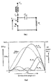
- Fig.1 the relationship between conduction angle and output power is illustrated in Fig.2 .
- the conduction angle 2 ⁇ means the period during which the switch is closed.
- ⁇ equals n/2, meaning that the switch is closed half of the time during the period of the input signal.
- the 2 nd harmonic output power is zero when ⁇ is n/2, and the 3 rd harmonic power becomes zero if ⁇ is n/3 or 2n/3. So if the conduction angle of the amplifier is well controlled, certain harmonic tones can be minimized. However, the real conduction angle of a practical amplifier is difficult to measure. For example, an amplifier for a WiFi system needs to work at 2.4GHz. The period of a 2.4GHz signal is 417 picoseconds. A conduction angle of n means the conduction time of the active element in the amplifier is only 208.5 picoseconds in each cycle. Directly measuring such a short time duration is extremely challenging.
- Patent US5712593 aims at maximizing efficiency while maintaining an allowable distortion level over the entire dynamic range of the power amplifiers.
- Fig.3 shows the block diagram of the disclosed circuit.
- Sampler 14 samples the output signal from amplifier 12 and provides the sampled signal to filter 16.
- Filter 16 filters out the desired signal and only passes through the undesired signals (harmonics or spurs) to detector 18.
- Detector 18 converts the filtered output signal to a DC signal proportional to the power level of the filtered output signal.
- Bias control portion 20 compares the DC signal provided by power detector 18 to a reference signal to produce a control signal.
- the control signal controls the saturation characteristics of power amplifier portion 12.
- Such a control loop continually re-biases the power amplifier for maximum efficiency for a desired level of distortion.
- Fig.3 can however only be used for linear amplifiers.
- the active device in power amplifier 12 must be in its linear region, so that the bias condition can be controlled by the feedback loop to change its linearity.
- a band reject filter 16 is needed to capture the non-linearity of the output signal by selecting the unwanted signals to be suppressed. It selects the unwanted signals that shall be suppressed, and its frequency response determines the cancellation performance of the system.
- detector 18 is needed to convert the RF signal from filter 16 to a readable DC signal. The presence of band reject filter 16 and detector 18 limits the flexibility of the proposed solution.
- the harmonic cancellation of the systems depends on the frequency response of the BPF, as it determines how well the unwanted signal is being filtered.
- the value of the reference voltage depends on (i) the required distortion level as defined by the user and (ii) on the voltage transfer function (VTC) of detector 18, which makes the selection of the reference voltage technology dependent.
- VTC voltage transfer function
- the invention relates to a circuit comprising
- the proposed circuit allows avoiding the occurrence of a given harmonic component when the signal output by the circuit is applied to a power amplifier.
- the buffering means converts the applied sinusoidal signal into a square wave.
- the DC level of this square wave signal forms an indication of the conduction angle of the power amplifier (i.e. the duty cycle of the square wave).
- the square wave signal is applied to a low pass filter in a feedback loop. This low pass filter filters out all the high frequency components of the output signal from the buffer, and lets the DC component pass through, in the sense that the filter output signal contains DC information of the input signal for the power amplifier.
- the measured DC level is compared to a voltage reference signal with a known level that is chosen for cancelling a given harmonic component, typically the second harmonic frequency.
- a correction signal is output to the buffering means to use for adjusting the threshold voltage, such that the DC level (and consequently the conduction angle) is adapted to bring the DC component of the square wave to a value whereby the influence of the given harmonic component can be eliminated.
- the circuit further comprises a second buffering means arranged for buffering the square wave signal received from the first buffering means and for outputting the buffered square wave signal via the output port.
- the second buffer is particularly useful for providing additional driving ability to drive the power amplifier.
- the circuit has a single-ended topology.
- the given harmonic component is an even order harmonic component, preferably the second harmonic frequency.
- the conduction angle is not directly measured as a time duration, but is derived in the voltage domain.
- the input DC voltage of the switching mode amplifier can be an indicator of its real conduction angle.
- the input signal of the amplifier is a square wave with, in this example, an amplitude normalized to 1.
- the conduction angle is shown as 2 ⁇ .
- the input signal can be written as Equation 1.
- V ⁇ ⁇ + 2 ⁇ ⁇ sin ⁇ cos ⁇ t + sin 2 ⁇ ⁇ 2 ⁇ cos 2 ⁇ ⁇ t + sin 3 ⁇ ⁇ 3 ⁇ cos 3 ⁇ ⁇ t + .. sin k ⁇ k ⁇ cosk ⁇ t
- Equation 2 V ⁇ 1 2 + ⁇ ⁇ + 2 ⁇ ⁇ cos ⁇ t - ⁇ cos ⁇ 2 ⁇ ⁇ t + cos 3 ⁇ ⁇ t 3 + ⁇ ⁇ So if the deviation ⁇ / ⁇ of the DC voltage is sensed, the value of ⁇ is known.
- the real conduction angle 2 ⁇ can be calculated and the conduction angle can be adjusted to make ⁇ zero and minmize the even-order harmonics.
- Fig.5 shows a scheme comprising the circuit 100 according to the present invention.
- the first buffer 10 converts the sinusoidal wave into a square wave.
- the second one (20) is optional and provides strong driving ability to drive the following stage.
- the output of the PA 30 may be connected to an antenna via a matching network which acts as a conventional impedance transfer block. The matching network does not affect the calibration as it is outside the feedback loop.
- the input signal of the PA 3, i.e. the signal output by the buffering means, is sensed by a low-pass filter (LPF) 40.
- LPF low-pass filter
- the LPF can be implemented as a simple passive first-order RC filter, the requirement is much relaxed compared to the band reject filter 16 in the prior art solution of Fig.3 .
- the LPF output 4 contains the DC information of the signal 3 that is inputted to the low pass filter. Comparator 50 then compares this DC voltage to a reference voltage Vref.
- Vref a reference voltage
- the DC term of the PA input voltage only relates to the conduction angle, so it is technology independent.
- the reference voltage which should be the benchmark of this DC voltage, is also technology independent.
- the loop changes the conduction angle of the PA and the harmonics emission energy is changed according to Fig.2 .
- the reference voltage should be equal to 1/2 for even order harmonics canncellation.
- the comparison result indicates whether the real conduction angle is larger or smaller than the optmized value.
- the threshold voltage (or bias condition) of the buffer can be adjusted to correct the duty cycle of the input signal of the power amplifier.
- the LPF 40 and the comparator 50 form a feedback loop which controls the duty cycle of the PA's input signal. Taking the even order harmonics as an example, if ⁇ is larger than n/2 (which means that ⁇ is positive), the LPF ouput is a voltage larger than 1/2. So the comparator returns a logic "high". Using this information, the threshold voltage of the buffer should be decreased by the calibration loop. Then the conduction angle is changed back to n. Such a calibration loop can continuously run to maintain the harmonic component below a certain level.
- the second buffer 20 in Fig.4 is optional. As the input impedance of the power amplifier is low, driving such a low impedance requires a buffer with strong driving ability and consumes lots of energy. In this case, using two cascade buffers connected in series is more efficient than using one large buffer. Providing this additional buffer is beneficial in that it allows reducing the size of the first buffer and the overall power consumption. To summarize, the first buffer brings the low-input swing to rail-to-rail level and drives the relatively small subsequent buffer which drives the power amplifier.
- the scheme of Fig.5 has, for the sake of simplicity, a single-ended topology. For differential architectures, it can also be separately applied to the two differential branches. For each branch the same calibration loop as used in Fig.5 is implemented, so the same functionality is achieved.
- the reference voltage can be set to 1/2 of the supply voltage to cancel out even-order harmonics if the matching of the two differential branches is poor. While it is set to 1/3 of the supply, the 3 rd harmonic is minimized.
- the LPF input port can be changed to connect at the power amplifier output, instead of the input of the PA as shown in Fig.5 .
- the output voltage waveform of the PA is affected by various other non-ideality effects inside the PA. So the PA input signal is much closer to an ideal square wave and it is better to be used as the input signal of the LPF.
- the configuration in Fig.5 has better accuracy.
- Fig.6 shows a Voltage Transfer Curve (VTC), which plots the buffer output voltage as a function of its input voltage.
- VTC Voltage Transfer Curve
- the threshold voltage is defined as the input voltage that make the output equal to the input.
- the duty cycle of the output signal is larger for a higher threshold voltage V t_high . If the threshold voltage is set as V t_low , then the duty cycle of the output signal is reduced.
- a buffer ciruit is implemented by connecting in parallel a plurality of identical unit buffer circuits.
- a unit buffer circuit comprises transistors M1 and M2 forming an inverter circuit, which are connected to power rails GND and VDD via transistors M0 and M3.
- the threshold voltage of the unit buffer depends on the bias current of the transistors M1 and M2.
- the bias current of transistor M1 can be controlled by adjusting the gate voltage of M0, while the bias current of transistor M2 is controlled by the gate voltage of M3.
- the gate voltages of M0 and M3 are shown in Fig.8 as the V bn and V bp voltages, respectively.
- both V bn and V bp voltages By increasing both V bn and V bp voltages, the bias current of M1 is increased, while the bias current of M2 is decreased. In this case, the threshold voltage is set to a lower value. On the oppsite side, for a higher threshold voltage, both V bn and V bp should be reduced. In the invention both V bn and V bp voltages can be controlled by the comparator to adjust the buffer threshold voltage.
- the proposed control circuit allows for adjusting the conduction angle of a power amplifier for a given harmonic component by simply changing the reference voltage applied at the comparator. It uses a simple passive LPF instead of complex extra RF filters, which are expensive and cause extra power losses. Also, the proposed circuit is easier to implement and integrate with the PA and it is suitable for both single-ended topology and differential PA topologies.
- a computer program may be stored/distributed on a suitable medium, such as an optical storage medium or a solid-state medium supplied together with or as part of other hardware, but may also be distributed in other forms, such as via the Internet or other wired or wireless telecommunication systems. Any reference signs in the claims should not be construed as limiting the scope.
Landscapes
- Engineering & Computer Science (AREA)
- Power Engineering (AREA)
- Amplifiers (AREA)
Abstract
- an input port for applying a sinusoidal input signal (1),
- a first buffering means (10) for converting the sinusoidal input signal into a square wave signal (2), the DC level of the square wave signal defined by an adjustable threshold voltage level, and a
- an output port for outputting the square wave signal to a power amplifier (30).
Description
- The present invention is generally related to the field of non-linear electronic devices like power amplifiers wherein harmonic components substantially affect the performance. More in particular, the invention relates to circuits for reducing or cancelling such effects.
- Switching mode power amplifiers, such as Class-D and Class-E amplifiers, are widely used nowadays due to their high efficiency. However, as highly non-linear devices, switching mode power amplifiers also generate quite an amount of energy at harmonic frequencies. Especially when using amplifiers with a single-ended output, the even-order harmonic tones are not cancelled out, as opposed to the amplifiers with an ideally differential output. The unwanted tones at the harmonic frequencies then violate the out-of-band spurious emission limits as defined by the ETSI or FCC standard regulation bodies.
- Electronic amplifiers are typically classified into classes, e.g. Class-A, B, C, D, E or even F. They can be grouped into two categories: linear amplifiers like Class A, B, C and switching mode amplifiers like Class D, E, F. The active element in a linear amplifier operates in the linear region, which means that the output signal is proportional to the input signal. A sinusoidal input signal results in a sinusoidal output with a larger amplitude. Switching mode amplifiers adopt a different operation principle. Normally, their input signal is a square wave to overdrive the active element. In this case the active element works like a switch : it is either completely on for conducting current or completely off. The output signal is then no longer proportional to the input signal. Notwithstanding the difference in operation principle, a conduction angle can be defined for these two categories in almost the same way. The conduction angle of an amplifier depends on the proportion of time during which the active element conducts current. For linear amplifiers the active element operates in the linear region when it is conducting and the output is proportional to the input. For switching amplifiers the active element works like a switch when conducting and the output is not proportional to the input. In the description below the conduction angle is referred to as 2α, so α represents half of the conduction angle. α ranges from 0 to n. If Class-A, the active element is always conducting, the conduction angle is 2n and thus α equals n. If Class-B, the active element is conducting for only half of each cycle of the input signal, the conduction angle is n and consequently α equals n/2. For switching mode amplifiers, the input signal is a square wave and the conduction angle is also equivalent to the duty cycle of the input square wave. If the duty cycle is 50%, the input voltage is high during half the period of each cycle and the active element conducts, so the conduction angle is n and α equals to n/2.
- The conduction angle of a switching mode amplifier is closely related to its harmonics emission performance. For an ideal switching mode amplifier with a broadband resistive load as shown in
Fig.1 , the relationship between conduction angle and output power is illustrated inFig.2 . As explained above, the conduction angle 2α means the period during which the switch is closed. Hence, α equals n/2, meaning that the switch is closed half of the time during the period of the input signal. - It is clear that the 2nd harmonic output power is zero when α is n/2, and the 3rd harmonic power becomes zero if α is n/3 or 2n/3. So if the conduction angle of the amplifier is well controlled, certain harmonic tones can be minimized. However, the real conduction angle of a practical amplifier is difficult to measure. For example, an amplifier for a WiFi system needs to work at 2.4GHz. The period of a 2.4GHz signal is 417 picoseconds. A conduction angle of n means the conduction time of the active element in the amplifier is only 208.5 picoseconds in each cycle. Directly measuring such a short time duration is extremely challenging.
- An obvious way to solve the harmonics emission problem would be to add an extra band-pass filter at the output of the amplifier to filter out any unwanted harmonics. However, such filter has to operate at radio frequencies (RF). High-performance RF band-pass filters are normally made of quartz or ceramics, which makes them difficult to be integrated with a power amplifier manufactured by modern semiconductor technology. Additionally, it introduces extra power loss. Another possible way would be to use a differential output topology to cancel out the even-order harmonics. However, due to poor matching of the two differential branches, the suppression effect is limited.
-
Patent US5712593 aims at maximizing efficiency while maintaining an allowable distortion level over the entire dynamic range of the power amplifiers.Fig.3 shows the block diagram of the disclosed circuit. Sampler 14 samples the output signal fromamplifier 12 and provides the sampled signal to filter 16. Filter 16 filters out the desired signal and only passes through the undesired signals (harmonics or spurs) todetector 18.Detector 18 converts the filtered output signal to a DC signal proportional to the power level of the filtered output signal.Bias control portion 20 compares the DC signal provided bypower detector 18 to a reference signal to produce a control signal. The control signal controls the saturation characteristics ofpower amplifier portion 12. Such a control loop continually re-biases the power amplifier for maximum efficiency for a desired level of distortion. - The scheme of
Fig.3 can however only be used for linear amplifiers. The active device inpower amplifier 12 must be in its linear region, so that the bias condition can be controlled by the feedback loop to change its linearity. Aband reject filter 16 is needed to capture the non-linearity of the output signal by selecting the unwanted signals to be suppressed. It selects the unwanted signals that shall be suppressed, and its frequency response determines the cancellation performance of the system. After this,detector 18 is needed to convert the RF signal fromfilter 16 to a readable DC signal. The presence ofband reject filter 16 anddetector 18 limits the flexibility of the proposed solution. First, the harmonic cancellation of the systems depends on the frequency response of the BPF, as it determines how well the unwanted signal is being filtered. Secondly, the value of the reference voltage depends on (i) the required distortion level as defined by the user and (ii) on the voltage transfer function (VTC) ofdetector 18, which makes the selection of the reference voltage technology dependent. Thus, selecting a proper reference voltage is not straightforward and requires complex calculation. - Hence, there is a need for a solution where the conduction angle can be controlled without undue burden, so that the influence a harmonic component can be reduced by adjusting the conduction angle.
- It is an object of embodiments of the present invention to provide for a circuit that allows reducing the effect of a given harmonic component on a power amplifier connected to the circuit.
- The above objective is accomplished by the solution according to the present invention.
- In a first aspect the invention relates to a circuit comprising
- an input port for applying a sinusoidal input signal,
- a first buffering means for converting the sinusoidal input signal into a square wave signal, the DC level of the square wave signal defined by an adjustable threshold voltage level, and
- an output port for outputting the square wave signal to a power amplifier.
- The proposed circuit allows avoiding the occurrence of a given harmonic component when the signal output by the circuit is applied to a power amplifier. The buffering means converts the applied sinusoidal signal into a square wave. The DC level of this square wave signal forms an indication of the conduction angle of the power amplifier (i.e. the duty cycle of the square wave). According to the invention the square wave signal is applied to a low pass filter in a feedback loop. This low pass filter filters out all the high frequency components of the output signal from the buffer, and lets the DC component pass through, in the sense that the filter output signal contains DC information of the input signal for the power amplifier. The measured DC level is compared to a voltage reference signal with a known level that is chosen for cancelling a given harmonic component, typically the second harmonic frequency. Depending on the comparison result a correction signal is output to the buffering means to use for adjusting the threshold voltage, such that the DC level (and consequently the conduction angle) is adapted to bring the DC component of the square wave to a value whereby the influence of the given harmonic component can be eliminated.
- In a preferred embodiment the circuit further comprises a second buffering means arranged for buffering the square wave signal received from the first buffering means and for outputting the buffered square wave signal via the output port. The second buffer is particularly useful for providing additional driving ability to drive the power amplifier.
- In an advantageous embodiment the circuit has a single-ended topology.
- In a preferred embodiment the given harmonic component is an even order harmonic component, preferably the second harmonic frequency.
- For purposes of summarizing the invention and the advantages achieved over the prior art, certain objects and advantages of the invention have been described herein above. Of course, it is to be understood that not necessarily all such objects or advantages may be achieved in accordance with any particular embodiment of the invention. Thus, for example, those skilled in the art will recognize that the invention may be embodied or carried out in a manner that achieves or optimizes one advantage or group of advantages as taught herein without necessarily achieving other objects or advantages as may be taught or suggested herein.
- The above and other aspects of the invention will be apparent from and elucidated with reference to the embodiment(s) described hereinafter.
- The invention will now be described further, by way of example, with reference to the accompanying drawings, wherein like reference numerals refer to like elements in the various figures.
-
Fig.1 illustrates an ideal switching mode amplifier. -
Fig.2 illustrates the relationship between conduction angle and output power. -
Fig.3 illustrates a prior art block diagram of the circuit presented inUS5712593 . -
Fig.4 illustrates a waveform of an input signal to be applied to a switching mode amplifier. -
Fig.5 illustrates a scheme comprising an embodiment of the circuit according to the invention. -
Fig.6 represents a Voltage Transfer Curve (VTC), which plots the buffer output voltage as a function of its input voltage. -
Fig.7 illustrates the effect of changing the threshold voltage on the output voltage. -
Fig.8 illustrates an implementation of the tuneable buffer circuit allowing for control of the threshold voltage. - The present invention will be described with respect to particular embodiments and with reference to certain drawings but the invention is not limited thereto but only by the claims.
- Furthermore, the terms first, second and the like in the description and in the claims, are used for distinguishing between similar elements and not necessarily for describing a sequence, either temporally, spatially, in ranking or in any other manner. It is to be understood that the terms so used are interchangeable under appropriate circumstances and that the embodiments of the invention described herein are capable of operation in other sequences than described or illustrated herein.
- It is to be noticed that the term "comprising", used in the claims, should not be interpreted as being restricted to the means listed thereafter; it does not exclude other elements or steps. It is thus to be interpreted as specifying the presence of the stated features, integers, steps or components as referred to, but does not preclude the presence or addition of one or more other features, integers, steps or components, or groups thereof. Thus, the scope of the expression "a device comprising means A and B" should not be limited to devices consisting only of components A and B. It means that with respect to the present invention, the only relevant components of the device are A and B.
- Reference throughout this specification to "one embodiment" or "an embodiment" means that a particular feature, structure or characteristic described in connection with the embodiment is included in at least one embodiment of the present invention. Thus, appearances of the phrases "in one embodiment" or "in an embodiment" in various places throughout this specification are not necessarily all referring to the same embodiment, but may. Furthermore, the particular features, structures or characteristics may be combined in any suitable manner, as would be apparent to one of ordinary skill in the art from this disclosure, in one or more embodiments.
- Similarly it should be appreciated that in the description of exemplary embodiments of the invention, various features of the invention are sometimes grouped together in a single embodiment, figure, or description thereof for the purpose of streamlining the disclosure and aiding in the understanding of one or more of the various inventive aspects. This method of disclosure, however, is not to be interpreted as reflecting an intention that the claimed invention requires more features than are expressly recited in each claim. Rather, as the following claims reflect, inventive aspects lie in less than all features of a single foregoing disclosed embodiment. Thus, the claims following the detailed description are hereby expressly incorporated into this detailed description, with each claim standing on its own as a separate embodiment of this invention.
- Furthermore, while some embodiments described herein include some but not other features included in other embodiments, combinations of features of different embodiments are meant to be within the scope of the invention, and form different embodiments, as would be understood by those in the art. For example, in the following claims, any of the claimed embodiments can be used in any combination.
- It should be noted that the use of particular terminology when describing certain features or aspects of the invention should not be taken to imply that the terminology is being redefined herein to be restricted to include any specific characteristics of the features or aspects of the invention with which that terminology is associated.
- In the description provided herein, numerous specific details are set forth. However, it is understood that embodiments of the invention may be practiced without these specific details. In other instances, well-known methods, structures and techniques have not been shown in detail in order not to obscure an understanding of this description.
- In the present invention the conduction angle is not directly measured as a time duration, but is derived in the voltage domain. The input DC voltage of the switching mode amplifier can be an indicator of its real conduction angle. As shown in
Fig.4 , the input signal of the amplifier is a square wave with, in this example, an amplitude normalized to 1. The conduction angle is shown as 2α. Applying Fourier expansion, the input signal can be written asEquation 1.
- where w denotes the fundamental frequency. The DC voltage is equal to α/π.
- To further explain the relationship between conduction angle and harmonics, the even-order harmonics are considered as an example. If α=π/2, all the even-order harmonics are zero, as can easily be seen from expression (1). However, if the conduction angle is slightly shifted from n (i.e. α deviates from n/2), the amplitudes of even-order harmonics cannot be neglected. With β denoting the deviation of α from n/2, the DC voltage (1/2 + β/π) also deviates from 1/2 and the second order harmonic amplitude (-2β/π) is proportional to the deviation value, as shown in Equation 2:

-
Fig.5 shows a scheme comprising thecircuit 100 according to the present invention. There are two buffers from the input port to the power amplifier 30 (PA). Thefirst buffer 10 converts the sinusoidal wave into a square wave. The second one (20) is optional and provides strong driving ability to drive the following stage. The output of thePA 30 may be connected to an antenna via a matching network which acts as a conventional impedance transfer block. The matching network does not affect the calibration as it is outside the feedback loop. The input signal of thePA 3, i.e. the signal output by the buffering means, is sensed by a low-pass filter (LPF) 40. The LPF can be implemented as a simple passive first-order RC filter, the requirement is much relaxed compared to the band rejectfilter 16 in the prior art solution ofFig.3 . The LPF output 4 contains the DC information of thesignal 3 that is inputted to the low pass filter.Comparator 50 then compares this DC voltage to a reference voltage Vref. As can be seen from expressions (1) and (2), the DC term of the PA input voltage only relates to the conduction angle, so it is technology independent. Hence, the reference voltage which should be the benchmark of this DC voltage, is also technology independent. By changing the reference voltage, the loop changes the conduction angle of the PA and the harmonics emission energy is changed according toFig.2 . For example, the reference voltage should be equal to 1/2 for even order harmonics canncellation. The comparison result then indicates whether the real conduction angle is larger or smaller than the optmized value. Based on the comparison result, the threshold voltage (or bias condition) of the buffer can be adjusted to correct the duty cycle of the input signal of the power amplifier. Thus, theLPF 40 and thecomparator 50 form a feedback loop which controls the duty cycle of the PA's input signal. Taking the even order harmonics as an example, if α is larger than n/2 (which means that β is positive), the LPF ouput is a voltage larger than 1/2. So the comparator returns a logic "high". Using this information, the threshold voltage of the buffer should be decreased by the calibration loop. Then the conduction angle is changed back to n. Such a calibration loop can continuously run to maintain the harmonic component below a certain level. - The
second buffer 20 inFig.4 is optional. As the input impedance of the power amplifier is low, driving such a low impedance requires a buffer with strong driving ability and consumes lots of energy. In this case, using two cascade buffers connected in series is more efficient than using one large buffer. Providing this additional buffer is beneficial in that it allows reducing the size of the first buffer and the overall power consumption. To summarize, the first buffer brings the low-input swing to rail-to-rail level and drives the relatively small subsequent buffer which drives the power amplifier. - The scheme of
Fig.5 has, for the sake of simplicity, a single-ended topology. For differential architectures, it can also be separately applied to the two differential branches. For each branch the same calibration loop as used inFig.5 is implemented, so the same functionality is achieved. The reference voltage can be set to 1/2 of the supply voltage to cancel out even-order harmonics if the matching of the two differential branches is poor. While it is set to 1/3 of the supply, the 3rd harmonic is minimized. - It is also worth mentioning that the LPF input port can be changed to connect at the power amplifier output, instead of the input of the PA as shown in
Fig.5 . However, in practice, the output voltage waveform of the PA is affected by various other non-ideality effects inside the PA. So the PA input signal is much closer to an ideal square wave and it is better to be used as the input signal of the LPF. In general, the configuration inFig.5 has better accuracy. - The functionality of the buffer is further explained in
Fig.6 . The buffer transfers a sinusoidal signal to a square wave.Fig.6 shows a Voltage Transfer Curve (VTC), which plots the buffer output voltage as a function of its input voltage. The VTC indicates that for a low input voltage, the circuit outputs a high voltage, whereas for high input voltage the output tapers off towards the low level. The threshold voltage is defined as the input voltage that make the output equal to the input. As illustrated inFig.7 , given the same input signal, the duty cycle of the output signal is larger for a higher threshold voltage Vt_high . If the threshold voltage is set as Vt_low, then the duty cycle of the output signal is reduced. By changing the threshold voltage of the buffer, the duty cycle of the PA Input signal is modified, hence the conduction angle of the PA is equivalently changed. - There are several possible ways to control the threshold voltage of the
buffer 10, such as changing the bias current. Typically, a buffer ciruit is implemented by connecting in parallel a plurality of identical unit buffer circuits. As shown inFig.8 , a unit buffer circuit comprises transistors M1 and M2 forming an inverter circuit, which are connected to power rails GND and VDD via transistors M0 and M3. The threshold voltage of the unit buffer depends on the bias current of the transistors M1 and M2. The bias current of transistor M1 can be controlled by adjusting the gate voltage of M0, while the bias current of transistor M2 is controlled by the gate voltage of M3. The gate voltages of M0 and M3 are shown inFig.8 as the Vbn and Vbp voltages, respectively. By increasing both Vbn and Vbp voltages, the bias current of M1 is increased, while the bias current of M2 is decreased. In this case, the threshold voltage is set to a lower value. On the oppsite side, for a higher threshold voltage, both Vbn and Vbp should be reduced. In the invention both Vbn and Vbp voltages can be controlled by the comparator to adjust the buffer threshold voltage. - An important advantage of the invention is that the proposed control circuit allows for adjusting the conduction angle of a power amplifier for a given harmonic component by simply changing the reference voltage applied at the comparator. It uses a simple passive LPF instead of complex extra RF filters, which are expensive and cause extra power losses. Also, the proposed circuit is easier to implement and integrate with the PA and it is suitable for both single-ended topology and differential PA topologies.
- While the invention has been illustrated and described in detail in the drawings and foregoing description, such illustration and description are to be considered illustrative or exemplary and not restrictive. The foregoing description details certain embodiments of the invention. It will be appreciated, however, that no matter how detailed the foregoing appears in text, the invention may be practiced in many ways. The invention is not limited to the disclosed embodiments.
- Other variations to the disclosed embodiments can be understood and effected by those skilled in the art in practicing the claimed invention, from a study of the drawings, the disclosure and the appended claims. In the claims, the word "comprising" does not exclude other elements or steps, and the indefinite article "a" or "an" does not exclude a plurality. A single processor or other unit may fulfil the functions of several items recited in the claims. The mere fact that certain measures are recited in mutually different dependent claims does not indicate that a combination of these measures cannot be used to advantage. A computer program may be stored/distributed on a suitable medium, such as an optical storage medium or a solid-state medium supplied together with or as part of other hardware, but may also be distributed in other forms, such as via the Internet or other wired or wireless telecommunication systems. Any reference signs in the claims should not be construed as limiting the scope.
Claims (4)
- Circuit (100) comprising- an input port for applying a sinusoidal input signal (1),- a first buffering means (10) for converting said sinusoidal input signal into a square wave signal (2), said square wave signal having a DC level defined by an adjustable threshold voltage level,- an output port for outputting said square wave signal to a power amplifier (30),characterised by a feedback loop comprising a low pass filtering means (40) arranged for filtering said square wave signal and comparing means (50) arranged for comparing the DC level of a filtered signal received from said low pass filtering means with a pre-set reference level, said reference level selected for cancelling a given harmonic component, said comparing means further arranged for outputting to said first buffering means (10) a correction signal for adjusting said threshold voltage level of said first buffering means.
- Circuit (100) as in claim 1, further comprising a second buffering means (20) arranged for buffering said square wave signal (2) received from said first buffering means and for outputting the buffered square wave signal via said output port.
- Circuit (100) as in claim 1 or 2, having a single-ended topology.
- Circuit (100) as in any of the previous claims, wherein said given harmonic component is an even order harmonic frequency.
Priority Applications (3)
| Application Number | Priority Date | Filing Date | Title |
|---|---|---|---|
| EP13196361.3A EP2884659B1 (en) | 2013-12-10 | 2013-12-10 | Harmonics Cancellation Circuit for a Power Amplifier |
| JP2014224383A JP6613024B2 (en) | 2013-12-10 | 2014-11-04 | Harmonic cancellation circuit for power amplifier |
| US14/566,505 US9407209B2 (en) | 2013-12-10 | 2014-12-10 | Harmonics cancellation circuit for a power amplifier |
Applications Claiming Priority (1)
| Application Number | Priority Date | Filing Date | Title |
|---|---|---|---|
| EP13196361.3A EP2884659B1 (en) | 2013-12-10 | 2013-12-10 | Harmonics Cancellation Circuit for a Power Amplifier |
Publications (2)
| Publication Number | Publication Date |
|---|---|
| EP2884659A1 true EP2884659A1 (en) | 2015-06-17 |
| EP2884659B1 EP2884659B1 (en) | 2016-08-24 |
Family
ID=49725067
Family Applications (1)
| Application Number | Title | Priority Date | Filing Date |
|---|---|---|---|
| EP13196361.3A Active EP2884659B1 (en) | 2013-12-10 | 2013-12-10 | Harmonics Cancellation Circuit for a Power Amplifier |
Country Status (3)
| Country | Link |
|---|---|
| US (1) | US9407209B2 (en) |
| EP (1) | EP2884659B1 (en) |
| JP (1) | JP6613024B2 (en) |
Families Citing this family (6)
| Publication number | Priority date | Publication date | Assignee | Title |
|---|---|---|---|---|
| DE102013201686A1 (en) * | 2013-02-01 | 2014-08-21 | Siemens Aktiengesellschaft | Method and circuit arrangement for converting a sine signal into a rectangular signal, and use thereof |
| US9641141B1 (en) | 2016-02-29 | 2017-05-02 | Hong Kong Applied Science and Technology Research Institute Company Limited | Harmonics suppression circuit for a switch-mode power amplifier |
| JP6754667B2 (en) | 2016-10-20 | 2020-09-16 | ルネサスエレクトロニクス株式会社 | Semiconductor device |
| IT201600110367A1 (en) * | 2016-11-03 | 2018-05-03 | St Microelectronics Srl | PROCEDURE FOR CHECKING AMPLIFIERS, CIRCUIT AND CORRESPONDING DEVICE |
| US10461701B2 (en) * | 2018-01-19 | 2019-10-29 | Silicon Laboratories Inc. | System and method for reducing output harmonics |
| US10630244B2 (en) * | 2018-03-16 | 2020-04-21 | Shenzhen GOODIX Technology Co., Ltd. | Pulse width distortion cancellation of a switching mode amplifier for reduced second harmonic interference |
Citations (3)
| Publication number | Priority date | Publication date | Assignee | Title |
|---|---|---|---|---|
| US5712593A (en) | 1996-02-05 | 1998-01-27 | Motorola, Inc. | Linear power amplifier with distortion detection |
| US20090146754A1 (en) * | 2007-12-11 | 2009-06-11 | Telefonaktiebolaget L M Ericsson (Publ) | Pulse-Width Modulator Methods and Apparatus |
| US20090238258A1 (en) * | 2006-06-27 | 2009-09-24 | Telefonaktiebolaget L M Ericsson (Publ) | Switched Mode Power Amplification |
Family Cites Families (15)
| Publication number | Priority date | Publication date | Assignee | Title |
|---|---|---|---|---|
| JPS5586215A (en) * | 1978-12-23 | 1980-06-28 | Matsushita Electric Ind Co Ltd | Doubling circuit |
| JPH02141018A (en) * | 1988-11-21 | 1990-05-30 | Nec Corp | Automatic duty adjusting clock generation circuit |
| JPH07114349B2 (en) * | 1988-12-28 | 1995-12-06 | 株式会社東芝 | Duty control circuit device |
| JP3137411B2 (en) * | 1992-03-09 | 2001-02-19 | 沖電気工業株式会社 | Clock duty compensation circuit |
| US5990712A (en) | 1997-10-03 | 1999-11-23 | Motorola, Inc. | Harmonic generator |
| US6472918B1 (en) * | 1999-08-23 | 2002-10-29 | Level One Communications, Inc. | Self-referencing slicer method and apparatus for high-accuracy clock duty cycle generation |
| WO2001026217A1 (en) * | 1999-09-30 | 2001-04-12 | Fujitsu Limited | High-frequency power amplifier |
| US7319763B2 (en) * | 2001-07-11 | 2008-01-15 | American Technology Corporation | Power amplification for parametric loudspeakers |
| US6731915B1 (en) | 2000-10-31 | 2004-05-04 | Nokia Corporation | Combined RF power detector and power precorrector |
| JP3753145B2 (en) * | 2003-04-21 | 2006-03-08 | Jsr株式会社 | Anisotropic conductive sheet and method for manufacturing the same, adapter device and method for manufacturing the same, and electrical inspection device for circuit device |
| JP2006191196A (en) * | 2004-12-28 | 2006-07-20 | Toshiba Corp | Power amplifier |
| JP2010506514A (en) | 2006-10-06 | 2010-02-25 | ビダール クリシュナマーシー ヴィクラム | System and method for on-chip IM3 reduction over a wide range of operating power |
| JP2009239330A (en) * | 2008-03-25 | 2009-10-15 | Nippon Telegr & Teleph Corp <Ntt> | Amplitude limit amplifier circuit |
| GB2519540B (en) * | 2013-10-23 | 2018-05-09 | Cirrus Logic Int Semiconductor Ltd | Class-D Amplifier Circuits |
| GB2550243B (en) * | 2014-08-29 | 2018-03-21 | Cirrus Logic Int Semiconductor Ltd | Class D amplifier circuit |
-
2013
- 2013-12-10 EP EP13196361.3A patent/EP2884659B1/en active Active
-
2014
- 2014-11-04 JP JP2014224383A patent/JP6613024B2/en active Active
- 2014-12-10 US US14/566,505 patent/US9407209B2/en active Active
Patent Citations (3)
| Publication number | Priority date | Publication date | Assignee | Title |
|---|---|---|---|---|
| US5712593A (en) | 1996-02-05 | 1998-01-27 | Motorola, Inc. | Linear power amplifier with distortion detection |
| US20090238258A1 (en) * | 2006-06-27 | 2009-09-24 | Telefonaktiebolaget L M Ericsson (Publ) | Switched Mode Power Amplification |
| US20090146754A1 (en) * | 2007-12-11 | 2009-06-11 | Telefonaktiebolaget L M Ericsson (Publ) | Pulse-Width Modulator Methods and Apparatus |
Non-Patent Citations (1)
| Title |
|---|
| MICHAEL NIELSEN ET AL: "A 2-GHz GaAs HBT RF Pulsewidth Modulator", IEEE TRANSACTIONS ON MICROWAVE THEORY AND TECHNIQUES, IEEE SERVICE CENTER, PISCATAWAY, NJ, US, vol. 56, no. 2, 1 February 2008 (2008-02-01), pages 300 - 304, XP011199708, ISSN: 0018-9480, DOI: 10.1109/TMTT.2007.913375 * |
Also Published As
| Publication number | Publication date |
|---|---|
| JP2015115946A (en) | 2015-06-22 |
| EP2884659B1 (en) | 2016-08-24 |
| US9407209B2 (en) | 2016-08-02 |
| US20150162878A1 (en) | 2015-06-11 |
| JP6613024B2 (en) | 2019-11-27 |
Similar Documents
| Publication | Publication Date | Title |
|---|---|---|
| US9407209B2 (en) | Harmonics cancellation circuit for a power amplifier | |
| KR102772486B1 (en) | Class-d amplifier with multiple independent output stages | |
| US8143944B2 (en) | Method and apparatus for sensing a current for varying impedance loads | |
| US8299852B2 (en) | Method and apparatus for a gain control circuit via a high frequency signal | |
| KR20160074651A (en) | Class-d amplifier circuits | |
| US10090813B2 (en) | Power amplifier | |
| JP2011066558A (en) | Class-d amplifier | |
| CN109388173A (en) | Current compensation circuit | |
| US10122326B2 (en) | Systems and methods providing loadline modulation of a power amplifier | |
| JPH06252662A (en) | Power amplifier | |
| CN111030605A (en) | A gain compression compensation circuit for radio frequency power amplifier | |
| EP3560100B1 (en) | Pulse width distortion cancellation of switching mode amplifier for reduced second harmonic interference | |
| US10153742B2 (en) | Active RC filters | |
| US12088258B2 (en) | Preamplifying circuit | |
| WO2022049888A1 (en) | Semiconductor circuit | |
| CN104931996B (en) | The signal condition system of Larger Dynamic fast pulse in radiation detection | |
| JP6474111B2 (en) | Differential sampling circuit with harmonic cancellation | |
| JPWO2018061386A1 (en) | Class D amplifier | |
| CN107800391A (en) | Compensation circuit, compensation method and amplification circuit | |
| TWI474614B (en) | Power amplifier | |
| JP2007124625A (en) | Class-d amplifier | |
| CN203039646U (en) | High-performance operational amplifier | |
| JP5351849B2 (en) | Amplifier circuit | |
| JP5776794B2 (en) | Amplifier circuit | |
| US7368984B2 (en) | Switching class A-B amplifier |
Legal Events
| Date | Code | Title | Description |
|---|---|---|---|
| PUAI | Public reference made under article 153(3) epc to a published international application that has entered the european phase |
Free format text: ORIGINAL CODE: 0009012 |
|
| 17P | Request for examination filed |
Effective date: 20131210 |
|
| AK | Designated contracting states |
Kind code of ref document: A1 Designated state(s): AL AT BE BG CH CY CZ DE DK EE ES FI FR GB GR HR HU IE IS IT LI LT LU LV MC MK MT NL NO PL PT RO RS SE SI SK SM TR |
|
| AX | Request for extension of the european patent |
Extension state: BA ME |
|
| R17P | Request for examination filed (corrected) |
Effective date: 20151007 |
|
| RBV | Designated contracting states (corrected) |
Designated state(s): AL AT BE BG CH CY CZ DE DK EE ES FI FR GB GR HR HU IE IS IT LI LT LU LV MC MK MT NL NO PL PT RO RS SE SI SK SM TR |
|
| GRAP | Despatch of communication of intention to grant a patent |
Free format text: ORIGINAL CODE: EPIDOSNIGR1 |
|
| RIC1 | Information provided on ipc code assigned before grant |
Ipc: H03F 3/217 20060101AFI20160223BHEP Ipc: H03F 1/02 20060101ALI20160223BHEP |
|
| INTG | Intention to grant announced |
Effective date: 20160316 |
|
| GRAS | Grant fee paid |
Free format text: ORIGINAL CODE: EPIDOSNIGR3 |
|
| GRAA | (expected) grant |
Free format text: ORIGINAL CODE: 0009210 |
|
| AK | Designated contracting states |
Kind code of ref document: B1 Designated state(s): AL AT BE BG CH CY CZ DE DK EE ES FI FR GB GR HR HU IE IS IT LI LT LU LV MC MK MT NL NO PL PT RO RS SE SI SK SM TR |
|
| REG | Reference to a national code |
Ref country code: GB Ref legal event code: FG4D |
|
| REG | Reference to a national code |
Ref country code: CH Ref legal event code: EP |
|
| REG | Reference to a national code |
Ref country code: AT Ref legal event code: REF Ref document number: 823864 Country of ref document: AT Kind code of ref document: T Effective date: 20160915 |
|
| REG | Reference to a national code |
Ref country code: IE Ref legal event code: FG4D |
|
| REG | Reference to a national code |
Ref country code: DE Ref legal event code: R096 Ref document number: 602013010571 Country of ref document: DE |
|
| REG | Reference to a national code |
Ref country code: FR Ref legal event code: PLFP Year of fee payment: 4 |
|
| REG | Reference to a national code |
Ref country code: LT Ref legal event code: MG4D |
|
| REG | Reference to a national code |
Ref country code: NL Ref legal event code: MP Effective date: 20160824 |
|
| REG | Reference to a national code |
Ref country code: AT Ref legal event code: MK05 Ref document number: 823864 Country of ref document: AT Kind code of ref document: T Effective date: 20160824 |
|
| PG25 | Lapsed in a contracting state [announced via postgrant information from national office to epo] |
Ref country code: LT Free format text: LAPSE BECAUSE OF FAILURE TO SUBMIT A TRANSLATION OF THE DESCRIPTION OR TO PAY THE FEE WITHIN THE PRESCRIBED TIME-LIMIT Effective date: 20160824 Ref country code: IT Free format text: LAPSE BECAUSE OF FAILURE TO SUBMIT A TRANSLATION OF THE DESCRIPTION OR TO PAY THE FEE WITHIN THE PRESCRIBED TIME-LIMIT Effective date: 20160824 Ref country code: HR Free format text: LAPSE BECAUSE OF FAILURE TO SUBMIT A TRANSLATION OF THE DESCRIPTION OR TO PAY THE FEE WITHIN THE PRESCRIBED TIME-LIMIT Effective date: 20160824 Ref country code: NO Free format text: LAPSE BECAUSE OF FAILURE TO SUBMIT A TRANSLATION OF THE DESCRIPTION OR TO PAY THE FEE WITHIN THE PRESCRIBED TIME-LIMIT Effective date: 20161124 Ref country code: RS Free format text: LAPSE BECAUSE OF FAILURE TO SUBMIT A TRANSLATION OF THE DESCRIPTION OR TO PAY THE FEE WITHIN THE PRESCRIBED TIME-LIMIT Effective date: 20160824 Ref country code: NL Free format text: LAPSE BECAUSE OF FAILURE TO SUBMIT A TRANSLATION OF THE DESCRIPTION OR TO PAY THE FEE WITHIN THE PRESCRIBED TIME-LIMIT Effective date: 20160824 Ref country code: FI Free format text: LAPSE BECAUSE OF FAILURE TO SUBMIT A TRANSLATION OF THE DESCRIPTION OR TO PAY THE FEE WITHIN THE PRESCRIBED TIME-LIMIT Effective date: 20160824 |
|
| PG25 | Lapsed in a contracting state [announced via postgrant information from national office to epo] |
Ref country code: PT Free format text: LAPSE BECAUSE OF FAILURE TO SUBMIT A TRANSLATION OF THE DESCRIPTION OR TO PAY THE FEE WITHIN THE PRESCRIBED TIME-LIMIT Effective date: 20161226 Ref country code: GR Free format text: LAPSE BECAUSE OF FAILURE TO SUBMIT A TRANSLATION OF THE DESCRIPTION OR TO PAY THE FEE WITHIN THE PRESCRIBED TIME-LIMIT Effective date: 20161125 Ref country code: SE Free format text: LAPSE BECAUSE OF FAILURE TO SUBMIT A TRANSLATION OF THE DESCRIPTION OR TO PAY THE FEE WITHIN THE PRESCRIBED TIME-LIMIT Effective date: 20160824 Ref country code: ES Free format text: LAPSE BECAUSE OF FAILURE TO SUBMIT A TRANSLATION OF THE DESCRIPTION OR TO PAY THE FEE WITHIN THE PRESCRIBED TIME-LIMIT Effective date: 20160824 Ref country code: LV Free format text: LAPSE BECAUSE OF FAILURE TO SUBMIT A TRANSLATION OF THE DESCRIPTION OR TO PAY THE FEE WITHIN THE PRESCRIBED TIME-LIMIT Effective date: 20160824 Ref country code: AT Free format text: LAPSE BECAUSE OF FAILURE TO SUBMIT A TRANSLATION OF THE DESCRIPTION OR TO PAY THE FEE WITHIN THE PRESCRIBED TIME-LIMIT Effective date: 20160824 |
|
| PG25 | Lapsed in a contracting state [announced via postgrant information from national office to epo] |
Ref country code: RO Free format text: LAPSE BECAUSE OF FAILURE TO SUBMIT A TRANSLATION OF THE DESCRIPTION OR TO PAY THE FEE WITHIN THE PRESCRIBED TIME-LIMIT Effective date: 20160824 Ref country code: EE Free format text: LAPSE BECAUSE OF FAILURE TO SUBMIT A TRANSLATION OF THE DESCRIPTION OR TO PAY THE FEE WITHIN THE PRESCRIBED TIME-LIMIT Effective date: 20160824 |
|
| REG | Reference to a national code |
Ref country code: DE Ref legal event code: R097 Ref document number: 602013010571 Country of ref document: DE |
|
| PG25 | Lapsed in a contracting state [announced via postgrant information from national office to epo] |
Ref country code: CZ Free format text: LAPSE BECAUSE OF FAILURE TO SUBMIT A TRANSLATION OF THE DESCRIPTION OR TO PAY THE FEE WITHIN THE PRESCRIBED TIME-LIMIT Effective date: 20160824 Ref country code: BE Free format text: LAPSE BECAUSE OF FAILURE TO SUBMIT A TRANSLATION OF THE DESCRIPTION OR TO PAY THE FEE WITHIN THE PRESCRIBED TIME-LIMIT Effective date: 20160824 Ref country code: PL Free format text: LAPSE BECAUSE OF FAILURE TO SUBMIT A TRANSLATION OF THE DESCRIPTION OR TO PAY THE FEE WITHIN THE PRESCRIBED TIME-LIMIT Effective date: 20160824 Ref country code: BG Free format text: LAPSE BECAUSE OF FAILURE TO SUBMIT A TRANSLATION OF THE DESCRIPTION OR TO PAY THE FEE WITHIN THE PRESCRIBED TIME-LIMIT Effective date: 20161124 Ref country code: DK Free format text: LAPSE BECAUSE OF FAILURE TO SUBMIT A TRANSLATION OF THE DESCRIPTION OR TO PAY THE FEE WITHIN THE PRESCRIBED TIME-LIMIT Effective date: 20160824 Ref country code: SM Free format text: LAPSE BECAUSE OF FAILURE TO SUBMIT A TRANSLATION OF THE DESCRIPTION OR TO PAY THE FEE WITHIN THE PRESCRIBED TIME-LIMIT Effective date: 20160824 Ref country code: SK Free format text: LAPSE BECAUSE OF FAILURE TO SUBMIT A TRANSLATION OF THE DESCRIPTION OR TO PAY THE FEE WITHIN THE PRESCRIBED TIME-LIMIT Effective date: 20160824 |
|
| PLBE | No opposition filed within time limit |
Free format text: ORIGINAL CODE: 0009261 |
|
| STAA | Information on the status of an ep patent application or granted ep patent |
Free format text: STATUS: NO OPPOSITION FILED WITHIN TIME LIMIT |
|
| REG | Reference to a national code |
Ref country code: CH Ref legal event code: PL |
|
| 26N | No opposition filed |
Effective date: 20170526 |
|
| PG25 | Lapsed in a contracting state [announced via postgrant information from national office to epo] |
Ref country code: SI Free format text: LAPSE BECAUSE OF FAILURE TO SUBMIT A TRANSLATION OF THE DESCRIPTION OR TO PAY THE FEE WITHIN THE PRESCRIBED TIME-LIMIT Effective date: 20160824 |
|
| PG25 | Lapsed in a contracting state [announced via postgrant information from national office to epo] |
Ref country code: MC Free format text: LAPSE BECAUSE OF FAILURE TO SUBMIT A TRANSLATION OF THE DESCRIPTION OR TO PAY THE FEE WITHIN THE PRESCRIBED TIME-LIMIT Effective date: 20160824 |
|
| REG | Reference to a national code |
Ref country code: IE Ref legal event code: MM4A |
|
| PG25 | Lapsed in a contracting state [announced via postgrant information from national office to epo] |
Ref country code: CH Free format text: LAPSE BECAUSE OF NON-PAYMENT OF DUE FEES Effective date: 20161231 Ref country code: LI Free format text: LAPSE BECAUSE OF NON-PAYMENT OF DUE FEES Effective date: 20161231 Ref country code: LU Free format text: LAPSE BECAUSE OF NON-PAYMENT OF DUE FEES Effective date: 20161210 |
|
| REG | Reference to a national code |
Ref country code: FR Ref legal event code: PLFP Year of fee payment: 5 |
|
| PG25 | Lapsed in a contracting state [announced via postgrant information from national office to epo] |
Ref country code: IE Free format text: LAPSE BECAUSE OF NON-PAYMENT OF DUE FEES Effective date: 20161210 |
|
| PG25 | Lapsed in a contracting state [announced via postgrant information from national office to epo] |
Ref country code: HU Free format text: LAPSE BECAUSE OF FAILURE TO SUBMIT A TRANSLATION OF THE DESCRIPTION OR TO PAY THE FEE WITHIN THE PRESCRIBED TIME-LIMIT; INVALID AB INITIO Effective date: 20131210 |
|
| PG25 | Lapsed in a contracting state [announced via postgrant information from national office to epo] |
Ref country code: CY Free format text: LAPSE BECAUSE OF FAILURE TO SUBMIT A TRANSLATION OF THE DESCRIPTION OR TO PAY THE FEE WITHIN THE PRESCRIBED TIME-LIMIT Effective date: 20160824 Ref country code: MK Free format text: LAPSE BECAUSE OF FAILURE TO SUBMIT A TRANSLATION OF THE DESCRIPTION OR TO PAY THE FEE WITHIN THE PRESCRIBED TIME-LIMIT Effective date: 20160824 Ref country code: IS Free format text: LAPSE BECAUSE OF FAILURE TO SUBMIT A TRANSLATION OF THE DESCRIPTION OR TO PAY THE FEE WITHIN THE PRESCRIBED TIME-LIMIT Effective date: 20160824 |
|
| PG25 | Lapsed in a contracting state [announced via postgrant information from national office to epo] |
Ref country code: MT Free format text: LAPSE BECAUSE OF NON-PAYMENT OF DUE FEES Effective date: 20161210 |
|
| PG25 | Lapsed in a contracting state [announced via postgrant information from national office to epo] |
Ref country code: AL Free format text: LAPSE BECAUSE OF FAILURE TO SUBMIT A TRANSLATION OF THE DESCRIPTION OR TO PAY THE FEE WITHIN THE PRESCRIBED TIME-LIMIT Effective date: 20160824 Ref country code: TR Free format text: LAPSE BECAUSE OF FAILURE TO SUBMIT A TRANSLATION OF THE DESCRIPTION OR TO PAY THE FEE WITHIN THE PRESCRIBED TIME-LIMIT Effective date: 20160824 |
|
| P01 | Opt-out of the competence of the unified patent court (upc) registered |
Effective date: 20230513 |
|
| PGFP | Annual fee paid to national office [announced via postgrant information from national office to epo] |
Ref country code: DE Payment date: 20251126 Year of fee payment: 13 |
|
| PGFP | Annual fee paid to national office [announced via postgrant information from national office to epo] |
Ref country code: GB Payment date: 20251119 Year of fee payment: 13 |
|
| PGFP | Annual fee paid to national office [announced via postgrant information from national office to epo] |
Ref country code: FR Payment date: 20251120 Year of fee payment: 13 |