EP2884366B1 - Self-adjusting delay circuit - Google Patents
Self-adjusting delay circuit Download PDFInfo
- Publication number
- EP2884366B1 EP2884366B1 EP13197006.3A EP13197006A EP2884366B1 EP 2884366 B1 EP2884366 B1 EP 2884366B1 EP 13197006 A EP13197006 A EP 13197006A EP 2884366 B1 EP2884366 B1 EP 2884366B1
- Authority
- EP
- European Patent Office
- Prior art keywords
- clock
- signal
- edge
- self
- circuit
- Prior art date
- Legal status (The legal status is an assumption and is not a legal conclusion. Google has not performed a legal analysis and makes no representation as to the accuracy of the status listed.)
- Not-in-force
Links
Images


Classifications
-
- G—PHYSICS
- G06—COMPUTING OR CALCULATING; COUNTING
- G06F—ELECTRIC DIGITAL DATA PROCESSING
- G06F1/00—Details not covered by groups G06F3/00 - G06F13/00 and G06F21/00
- G06F1/04—Generating or distributing clock signals or signals derived directly therefrom
-
- G—PHYSICS
- G06—COMPUTING OR CALCULATING; COUNTING
- G06F—ELECTRIC DIGITAL DATA PROCESSING
- G06F1/00—Details not covered by groups G06F3/00 - G06F13/00 and G06F21/00
- G06F1/04—Generating or distributing clock signals or signals derived directly therefrom
- G06F1/12—Synchronisation of different clock signals provided by a plurality of clock generators
-
- H—ELECTRICITY
- H03—ELECTRONIC CIRCUITRY
- H03K—PULSE TECHNIQUE
- H03K5/00—Manipulating of pulses not covered by one of the other main groups of this subclass
- H03K5/13—Arrangements having a single output and transforming input signals into pulses delivered at desired time intervals
- H03K5/131—Digitally controlled
-
- H—ELECTRICITY
- H03—ELECTRONIC CIRCUITRY
- H03L—AUTOMATIC CONTROL, STARTING, SYNCHRONISATION OR STABILISATION OF GENERATORS OF ELECTRONIC OSCILLATIONS OR PULSES
- H03L7/00—Automatic control of frequency or phase; Synchronisation
- H03L7/06—Automatic control of frequency or phase; Synchronisation using a reference signal applied to a frequency- or phase-locked loop
- H03L7/08—Details of the phase-locked loop
- H03L7/081—Details of the phase-locked loop provided with an additional controlled phase shifter
- H03L7/0812—Details of the phase-locked loop provided with an additional controlled phase shifter and where no voltage or current controlled oscillator is used
- H03L7/0816—Details of the phase-locked loop provided with an additional controlled phase shifter and where no voltage or current controlled oscillator is used the controlled phase shifter and the frequency- or phase-detection arrangement being connected to a common input
-
- H—ELECTRICITY
- H04—ELECTRIC COMMUNICATION TECHNIQUE
- H04L—TRANSMISSION OF DIGITAL INFORMATION, e.g. TELEGRAPHIC COMMUNICATION
- H04L7/00—Arrangements for synchronising receiver with transmitter
- H04L7/0016—Arrangements for synchronising receiver with transmitter correction of synchronization errors
- H04L7/0033—Correction by delay
- H04L7/0037—Delay of clock signal
-
- H—ELECTRICITY
- H03—ELECTRONIC CIRCUITRY
- H03K—PULSE TECHNIQUE
- H03K5/00—Manipulating of pulses not covered by one of the other main groups of this subclass
- H03K2005/00013—Delay, i.e. output pulse is delayed after input pulse and pulse length of output pulse is dependent on pulse length of input pulse
- H03K2005/00019—Variable delay
- H03K2005/00058—Variable delay controlled by a digital setting
- H03K2005/00071—Variable delay controlled by a digital setting by adding capacitance as a load
Definitions
- the invention relates to an apparatus for self-adjustment of a received clock signal provided for a received data signal.
- Integrated circuits in particular VLSI circuits, can contain several thousands of latches so that the total wire length of a clock signal supply line can exceed several millimetres within the integrated chip.
- the clock frequency of a clock signal is in many applications maximized to achieve a high-system performance of the integrated circuit.
- a combination of a relatively high clock frequency and a large clock load can cause severe timing problems.
- pipeline or scan registers integrated in the circuit are implemented by using serial connections of flip-flops. Especially, in a scan mode during testing of the integrated circuit, flip-flops can be directly connected to other flip-flops.
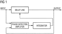
- the delay circuit illustrated in Fig. 1 comprises a delay line which can include some inverters and an integrating chain (RC-delay).
- the delay of the delay line can be controlled by the output voltage of an integrator as shown in Fig. 1 .
- RC-delay line a main disadvantage of the conventional delay circuit shown in Fig. 1 is that the delay provided by the delay line is dependent on the used manufacturing process technology. Depending on the employed technology process the provided delay of the delay line can vary between 10 and 100%. In many applications, this wide variation delay is unacceptable.
- the delay circuit shown in Fig. 1 further comprises a phase detector/amplifier.
- a delay of the DLL circuit is susceptible to supply noise which can in some cases depend on supply voltage variations within a supply voltage range.
- the clock edge counter is a ripple counter comprising a predetermined number of flip-flops connected in series to each other.
- the inverters of the adjustable delay line are three-state inverters each being enabled by a bit of the n-bit counter value output by the clock edge counter to invert the received clock signal with a driving current strength corresponding to the significance of the respective enabling bit.
- a reset detector circuit is provided adapted to generate in response to a reset signal a single pulse to set the flip-flops of the clock edge counter.
- a clock edge detector circuit is provided adapted to detect falling and/or rising signal edges of the received clock signal.
- the reset detector circuit and the clock edge detector circuit are connected via an OR gate to a clock input of the clock edge counter.
- an output of the edge comparator is set if the rising signal edge of the received data signal appears before a rising signal edge of the delayed clock signal output by the adjustable delay line.
- the edge comparator disables directly or via the phase margin security circuit the clock edge detector circuit as soon as the rising signal edge of the received data signal precedes the rising signal edge of the delayed clock signal output by the adjustable delay line.
- the received data signal is forwarded directly or via a buffer circuit of said self-adjusting delay circuit.
- the clock edge counter, the edge comparator and the phase margin security circuit comprise the same type of flip-flops.
- the flip-flops of the clock edge counter, the edge comparator and the phase margin security circuit comprise D-flip-flops.
- a delay-locked loop circuit comprises a self-adjusting delay circuit according to the present invention.
- the self-adjusting delay circuit 1 is adapted to delay a received clock signal CLK applied to a clock input 2 provided for a received data signal (data) received at a data input 3 of the self-adjusting delay circuit 1.
- the self-adjusting delay circuit 1 comprises a clock edge counter 4 adapted to count signal edges (e.g. falling signal edges) of the received clock signal CLK.
- the clock edge counter 4 is adapted to provide an incremented n-bit counter value applied to an adjustable delay line 5 having a corresponding number of inverters connected to each other in parallel, wherein each inverter is enabled by an associated bit of the n-bit counter value applied by the clock edge counter 4 to invert the received clock signal CLK with a driving current strength of the inverter corresponding to the significance of the respective bit of the n-bit counter value to load at least one capacitor of the adjustable delay line 5.
- the clock edge counter 4 applies an incremented 4-bit counter value to an adjustable delay line 5 having a corresponding number of inverters being connected to each other in parallel and being connected in parallel to an inverter receiving directly the clock signal CLK applied to the input 2 of the self-adjusting delay circuit 1.
- Fig. 3 shows a circuit diagram of an exemplary embodiment of the adjustable delay line 5 connected to the output of a clock edge counter 4.
- the clock edge counter 4 can be in a possible embodiment be a ripple counter comprising a predetermined number of flip-flops connected in series to each other as illustrated in the circuit diagram of Fig. 4 .
- the self-adjusting delay circuit 1 as shown in Fig.
- the received clock signal CLK is delayed by the adjustable delay line 5 with a stepwise increasing time delay, wherein the time delay is proportional to the incremented n-bit counter value output by the clock edge counter 4 until an edge comparator detects that a rising signal edge of the received data signal (data) precedes a rising signal edge of the delayed clock signal (CLK') output by the adjustable delay line 5.
- the output of the adjustable delay line 5 is connected via a clock signal line 6 to a clock input 7 and an edge comparator 8 which comprises in the shown exemplary embodiment a D-flip-flop 9 having a data input 10 receiving the data signal (data) via a signal line 11.
- the edge comparator 8 compares the signal edges of the received data signal (data) with the signal edges of the delayed clock signal CLK' output by the adjustable delay line 5 to detect when a rising signal edge of the received data signal precedes a rising signal edge of the delayed clock signal CLK'.
- the received clock signal CLK is delayed by the adjustable delay line 5 with an increasing time delay being proportional to the incremented n-bit counter value output by the clock edge counter 4 until the edge comparator 8 detects that a rising signal edge of the received data signal precedes a rising signal edge of the delayed clock signal CLK'.
- the D-flip-flop 9 comprises an output 11 wherein said output is set if the rising signal edge of the received data signal appears before a rising signal edge of the delayed clock signal output by the adjustable delay line 5.
- a phase margin security circuit 12 which comprises a predetermined number of flip-flops connected in series to each other.
- the phase margin security circuit 12 is provided to secure a phase margin and consists in the shown exemplary embodiment of three flip-flops 13-1, 13-2, 13-3.
- the flip-flops 13-i of the phase margin security circuit 12 are formed by D-flip-flops each having a clock input connected to the clock signal line 6 and receiving the delayed clock signal CLK' output by the adjustable delay line 5.
- Each D-flip-flop 13-i of the phase margin security circuit 12 has a data input (D) connected to the output of the preceding flip-flop 13-(i-1), wherein the first flip-flop 13-1 of the phase margin security circuit 12 is connected to the output 11 of the D-flip-flop forming the edge comparator 8.
- each D-flip-flop 9, 13-i comprises a preset input PRE for settings and a clear input CLR for resetting the flip-flops.
- the edge comparator 8 and the phase margin security circuit 12 are implemented by using the same type of flip-flops, i.e. D-flip-flops.
- the phase margin security circuit 12 comprises three flip-flops, but the number of flip-flops can vary depending on the requirements of the set-up time.
- a predetermined number of flip-flops is connected in series to each other, wherein the inverted output 14 of the last flip-flop supplies a counter stop signal in the shown embodiment via a signal line 15 to an AND gate 16 of a clock edge detector circuit 17 as shown in Fig. 2 .
- the clock edge detector circuit 17 is adapted to detect in the shown exemplary embodiment falling signal edges of the received clock signal CLK applied to the input 2 of the self-adjusting delay circuit 1.
- the clock edge detector a... ..
- the 17 comprises the AND gate 16 having three inputs A, B, C, wherein the third input C receives via the signal line 15 a count stop signal from the output of the phase margin security circuit 12.
- the first input A of the AND gate 16 within the clock edge detector circuit 17 receives the received clock signal CLK directly via an inverter circuit 18.
- the second input B of the AND gate 16 receives the clock signal CLK via two buffer circuits 19, 20 comprising a RC-delay circuit 21 in-between.
- the RC delay circuit 21 comprises in the shown exemplary embodiment a resistor R with a predetermined resistance and a capacitor C with a predetermined capacitance. In a possible embodiment, the resistance of the resistor within the RC delay circuit 21 and the capacitance of the capacitor within RC delay the circuit 21 can be adjustable.
- the output of the AND gate 16 within the clock edge detector circuit 17 is connected to a first input of an OR gate 22 having a second input connected to the output of a reset detector circuit 23.
- the output of the OR gate 22 is connected via a line 24 to an clock input 25 of the clock edge counter 4 as also illustrated in Fig. 4 .
- the reset detector circuit 23 is adapted to generate in response to a reset signal RST applied to a reset input 26 of the self-adjusting delay circuit 1 a signal pulse to set all flip-flops within the clock edge counter 4.
- the clock edge counter 4 comprises a ripple counter.
- each D-flip-flop 27-i of the clock edge counter 4 comprises a clock input being connected to the data output of the previous flip-flop.
- the data input D of each D-flip-flop 27-i is connected to the inverted data output Q of the same flip-flop.
- each D-flip-flop comprises a preset input PRE connected to a fixed potential and a clear input CLR connected to a reset input 31 of the clock edge counter 4 as illustrated in Fig. 4 .
- the ripple counter 4 is an asynchronous counter having a first flip-flop 27-1 being clocked by the external clock signal CLK. All subsequent flip-flops 27-i are clocked by the output of the preceding flip-flop.
- the MOD of the ripple counter is 2 n when n-flip-flops are used.
- the count range of the count value is 0000 to 1111.
- the counter value is incremented stepwise, wherein the count sequence does repeat itself.
- the ripple counter 4 is implemented by using D-flip-flops.
- the self-adjusting delay circuit 1 has a reset input terminal 26 which is connected via a reset line 32 to a node 33 being connected via a reset line 34 to the reset input 31 of the clock edge counter 4 and via a reset line 35 to the clear inputs CLR of the D-flip-flops within the edge comparator 8 and the phase margin security circuit 12 as illustrated in Fig. 2 .
- a reset line 32 is connected via a reset line 32 to a node 33 being connected via a reset line 34 to the reset input 31 of the clock edge counter 4 and via a reset line 35 to the clear inputs CLR of the D-flip-flops within the edge comparator 8 and the phase margin security circuit 12 as illustrated in Fig. 2 .
- the clock edge detector circuit 17 and the reset detector circuit 23 are both connected via the OR gate 22 to the clock input 25 of the clock edge counter 4.
- the edge comparator 8 enables in the shown embodiment via the phase margin security circuit 12 the clock edge detector circuit 17 as soon as the rising signal edge of the received data signal (data) precedes the rising signal edge of the delayed clock signal CLK' output by the adjustable delay line 5.
- the received data signal applied to the data input 3 of the self-adjusting delay circuit 1 is in a possible embodiment forwarded directly.
- the received data signal is forwarded via a buffer circuit 36 to a data output terminal 37 of the self-adjusting delay circuit 1.
- a buffer circuit 36 to a data output terminal 37 of the self-adjusting delay circuit 1.
- the reset detector circuit 23 comprises a first buffer circuit 38 connected via an RC delay circuit 39 to a second buffer circuit 40 whose output is connected to the input of an inverter circuit 41 and to an output of a further buffer circuit 42.
- the output of the buffer circuit 42 is connected via a further RC delay circuit 43 to the input of a buffer circuit 44.
- the output of the inverter circuit 41 and the output of the buffer circuit 44 are connected to corresponding inputs of an AND gate 45 of the reset detector circuit 23.
- the output of the AND gate 45 is connected with the second input of the OR gate 22 as illustrated in Fig. 2 . In the shown embodiment of Fig.
- the delayed clock signal CLK' output by the adjustable delay line 5 is applied via a buffer circuit 46 to a clock output terminal 47 for the delayed clock signal output by the self-adjusting delay circuit 1.
- Fig. 5 shows a possible exemplary embodiment of the adjustable delay line 5 within the self-adjusting delay circuit 1.
- the adjustable delay line 5 comprises a clock input 48 connected via a clock line 49 to the clock input 2 of the self-adjusting delay circuit 1. Accordingly, the clock input 48 receives directly the applied clock signal CLK.
- the adjustable delay line 5 comprises a number of inverters 50-1, 50-2, 50-3, 50-4 being connected to each other in parallel and being enabled by a corresponding bit of the n-bit counter value received from the clock edge counter 4. As can be seen in Fig.
- each of the parallel inverters 50-i is enabled via an internal line 51-i connected to an enabling bit input terminal 29-i of the adjustable delay line 5.
- the adjustable delay line 5 further comprises an inverter 50-0 whose input is connected via an inverter 52 to the clock input 48 of the adjustable delay line 5.
- the inverters 50-i are connected to each other in parallel, as illustrated in Fig. 3 .
- the inverters 50-1, 50-2, 50-3, 50-4 are enabled by an associated bit of the n-bit counter value to invert the received clock signal, wherein the driving current strength of the respective inverter does correspond to the bit-significance of the respective bit of the n-bit counter value to load a capacitor 53 of the adjustable delay line 5.
- the inverter 50-1 is enabled by the bit of the counter value having the least significance (LSB) and the inverter 50-4 is enabled by the bit of the counter value having the highest or most significance (MSB). Accordingly, in the shown embodiment, the lowest significant bit LSB of the counter value enables the inverter 50-1, wherein the most significant bit MSB enables the inverter 50-4 with the highest current driving strength.
- the inverters 50-0 has in the shown exemplary embodiment a predetermined driving strength of 4 corresponding to the driving strength of the inverter 52 and corresponding to the number of bits of the n-bit counter value.
- the capacitor 53 has a predetermined capacitance of 1 p F .
- the time delay provided by the adjustable delay line 5 depends on the driving strength of the inverters and the capacitance C of the capacitor 53.
- the outputs of the inverters 50-0 to 50-4 are all connected to a common node 54.
- the capacitor 53 is connected between the common node 54 and a node 55 at a predetermined potential as illustrated in Fig. 3 .
- node 54 is connected via two serial connected buffer circuits 56, 57 to the clock output 58 of the adjustable delay line 5 supplying a delayed clock signal CLK' via the buffer circuit 46 to the output clock terminal 57 of the self-adjusting delay circuit 1. Further, the delayed clock signal CLK' is applied via the clock line 6 to the edge detector circuit 8 and the phase margin security circuit 12.
- Fig. 5 shows a circuit diagram of an exemplary embodiment of a three-state inverter which can be used in the adjustable delay line 5 for the inverter circuits 50-1, 50-2, 50-3, 50-4.
- each three-state inverter 50-i comprises a signal input 59 and an enable control input 60.
- the signal input 59 is connected within the adjustable delay line 5 via a corresponding internal line 61 to a common node 62 to receive the inverted clock signal.
- the enable control input 60 is connected via internal control lines 51-1, 51-i to a corresponding control input 29-i of the adjustable delay line 5.
- the three-state inverter 50-i comprises an internal inverter 63 connected to the gate of a PMOS M3.
- the enable control input 60 is connected via the internal inverter 63 to the control gate of the PMOS M3 and directly via an internal line 64 to the gate of an NMOS M4.
- the signal input 59 connected to the node 62 is applied to the gate of a PMOS M1 and to the gate of a complementary NMOS M2 as illustrated in Fig. 5 .
- the three-state inverter 50-i illustrated in Fig. 5 inverts the received signal applied to the signal input 59 with a predetermined current strength of the internal inverter 63, if the enable control input 60 receives an enabling signal, i.e. a bit of the n-bit counter value.
- the output 65 of the three-state inverter 50-i is connected to node 54 of the adjustable delay line 5 shown in Fig. 3 .
- the self-adjusting delay circuit 1, as shown in the embodiment of Fig. 2 comprises four main sub-blocks including the adjustable delay line 5, the clock edge counter 4, the clock edge detector circuit 17 and the phase margin security circuit 12 which secures a predetermined phase or time margin.
- the clock edge counter 4 in the embodiment shown in Fig. 2 comprises a 4-bit counter, but it can be in different embodiments of different size depending on the desired precision.
- the number of the counter bits of the n-bit counter value defines a correction step size, step number and correction range.
- the phase margin security circuit 12 secures the phase margin comprising in the shown embodiment of Fig.
- the edge comparator 8 can use the same type of flip-flops as the phase margin security circuit 12. Some additional logic is used to adjust delays for the signal. In a possible embodiment, these logic blocks can be placed in the input pads. All other sub-blocks of the self-adjusting delay circuit 1 can be placed in a possible embodiment close to the shift register or latch for which these inputs form the signal shape. At a power-up sequence, a reset of all flip-flops is done. On outputs 28-i of the clock edge counter 4 a low bit value "0" is provided.
- the falling edge of the POR (Power on Reset) signal by use of the falling edge detector creates a short pulse which through the OR gate 22 is applied to the clock input 25 of the clock edge counter 4.
- all flip-flops are set to a logical high value "1" at their outputs.
- all three-state inverters 50-i of the adjustable delay line 5 are enabled and the resulting delay of the adjustable delay line 5 is small.
- a sequence of RZ (Return Zero) only "1" is applied at the data input. This data is also applied to the data input of the edge detector.
- the clock signal CLK' delayed by the adjustable delay line 5 is applied to the clock input 7 of the edge comparator 8. If the set-up time is not enough, the edge comparator 8 samples a logical low value "0". The following clock period causes a change in the counter status. It enables an inverter with a lower driving capability and disables one with a higher driving capability so that the total strength of the parallel connected three-state inverters is reduced slightly and the delay of the adjustable delay line 5 increases.
- the edge comparator 8 comprising the D-flip-flop 9 is clocked now with a slightly more delayed clock signal. If the set-up time is still not enough, this process is repeated until the set-up time becomes sufficient to trigger the flip-flop 9 of the edge comparator 8.
- the logical high value "1" which does appear on its output is sampled by the phase margin security circuit 12. After two clock periods, the sampled signal appears at the circuitry output of the phase margin circuit 12. The inverted signal gates further the clock signal for the clock edge counter 4 which keeps its state until the power-down of the chip. A few additional delay steps create a security margin needed because of the noise and the possible clock jitter of the clock signal. In case that two clock periods (two adjustment steps) are not provided with enough security margin, it is possible to add further flip-flops in a pipeline within the phase margin security circuit 12. To achieve the desired phase margin, each flip-flop can add one adjustment step to the margin (4-bit counter in the self-adjusting delay line 5 corresponds to 16 adjustment steps).
- the gated clock signal stops at the input of the clock edge counter 4 and thus remains in this status keeping the adjustable delay line 5 adjusted with the necessary fitting time delay. It is possible that the value is recorded in the counter giving an optimal delay time. This optimal delay time can be written in an OTP (One Time Programmable) to program the adjustable delay line 5.
- OTP One Time Programmable
- Fig. 6 shows signal diagrams for illustrating the operation of a self-adjusting delay circuit 1 according to the present invention as illustrated in Fig. 2 .
- Fig. 6A shows the power on reset (POR) signal making a short pulse which through the OR gate 22 is applied to the clock input 25 of the clock edge counter 4.
- Figs. 6B, 6C, 6D, 6E illustrate different counter output bits of a 4-bit clock edge counter 4, as shown in the embodiment of Fig. 2 .
- Fig. 6F illustrates the counter input signal.
- Fig. 6H shows the margin generation output by the phase margin security circuit 12 of the self-adjusting delay circuit 1.
- Fig. 6I shows the SADL edge detector output of the edge comparator 8.
- Fig. 6J illustrates input data and Fig.
- the self-adjusting delay circuit 1 With the self-adjusting delay circuit 1 according to the present invention it is possible that the time delay of the adjustable delay line 5 is adjusted for different technology process parameters. Moreover, the delay of the delay line can be adjusted for different power supply voltages. The adjustment of the delay guarantees that each received data packet or data can be sampled correctly.
- the power consumption of the self-adjusting delay circuit 1 after adjustment is equal to a conventional RC-delay line. Accordingly, no additional power is required and the self-adjusting delay circuit 1 does not consume more electrical power than conventional delay lines.
- the self-adjusting delay circuit 1 according to the present invention can handle process variations and parasitic elements caused by the circuit design.
- the delay circuit according to the present invention is self-adjusting.
- the self-adjusting delay circuit 1 according to the present invention can be used in any circuits to delay a clock signal guaranteeing in this way a set-up time independently on the power supply range and the technology parameter variations.
Landscapes
- Engineering & Computer Science (AREA)
- Theoretical Computer Science (AREA)
- Physics & Mathematics (AREA)
- General Engineering & Computer Science (AREA)
- General Physics & Mathematics (AREA)
- Nonlinear Science (AREA)
- Computer Networks & Wireless Communication (AREA)
- Signal Processing (AREA)
- Pulse Circuits (AREA)
Description
- The invention relates to an apparatus for self-adjustment of a received clock signal provided for a received data signal.
Integrated circuits, in particular VLSI circuits, can contain several thousands of latches so that the total wire length of a clock signal supply line can exceed several millimetres within the integrated chip. The clock frequency of a clock signal is in many applications maximized to achieve a high-system performance of the integrated circuit. A combination of a relatively high clock frequency and a large clock load can cause severe timing problems.
In many chip designs, pipeline or scan registers integrated in the circuit are implemented by using serial connections of flip-flops. Especially, in a scan mode during testing of the integrated circuit, flip-flops can be directly connected to other flip-flops. This direct connection between the flip-flops results in that the propagation time of the data between these flip-flops is also very short. Since the clock signal is routed through these blocks automatically, its time of arrival at the first flip-flop of a different logic block can be earlier than the arrival time of the corresponding data signal. This can occur also when the input pads or paths of the data signal and clock signal have different delays or when these signals are applied from external signal sources in an incorrect manner, for example if the data set-up time does not satisfy the requirements of the respective flip-flops which have to latch the corresponding data. In these cases, it is necessary to delay the clock signal so that a proper data sampling can be guaranteed. For this purpose, delay circuits are used.
Fig. 1 shows a circuit diagram of a conventional delay circuit comprising a delay-locked loop DLL. The delay circuit illustrated inFig. 1 comprises a delay line which can include some inverters and an integrating chain (RC-delay). The delay of the delay line can be controlled by the output voltage of an integrator as shown inFig. 1 . For the RC-delay line, a main disadvantage of the conventional delay circuit shown inFig. 1 is that the delay provided by the delay line is dependent on the used manufacturing process technology. Depending on the employed technology process the provided delay of the delay line can vary between 10 and 100%. In many applications, this wide variation delay is unacceptable. The delay circuit shown inFig. 1 further comprises a phase detector/amplifier. For the delay line used in the delay-locked loop as shown inFig. 1 , a delay of the DLL circuit is susceptible to supply noise which can in some cases depend on supply voltage variations within a supply voltage range. - Prior art delay circuits are described in the documents
US 2004/150438 andUS 2001/054922 . - Accordingly, it is an object of the present invention to provide an apparatus which provides an adjustable delay with a minimal delay variation.
- This object is achieved according to the present invention by a self-adjusting delay circuit according to
claim 1. - In a possible embodiment of the self-adjusting delay circuit according to the present invention, the clock edge counter is a ripple counter comprising a predetermined number of flip-flops connected in series to each other.
In a further possible embodiment of the self-adjusting delay circuit according to the present invention, the inverters of the adjustable delay line are three-state inverters each being enabled by a bit of the n-bit counter value output by the clock edge counter to invert the received clock signal with a driving current strength corresponding to the significance of the respective enabling bit. - In a still further possible embodiment of the self-adjusting delay circuit according to the present invention, a reset detector circuit is provided adapted to generate in response to a reset signal a single pulse to set the flip-flops of the clock edge counter.
In a further possible embodiment of the self-adjusting delay circuit according to the present invention, a clock edge detector circuit is provided adapted to detect falling and/or rising signal edges of the received clock signal.
In a further possible embodiment of the self-adjusting delay circuit according to the present invention, the reset detector circuit and the clock edge detector circuit are connected via an OR gate to a clock input of the clock edge counter.
In a further possible embodiment of the self-adjusting delay circuit according to the present invention, an output of the edge comparator is set if the rising signal edge of the received data signal appears before a rising signal edge of the delayed clock signal output by the adjustable delay line. - In a still further possible embodiment of the self-adjusting delay circuit according to the present invention, the edge comparator disables directly or via the phase margin security circuit the clock edge detector circuit as soon as the rising signal edge of the received data signal precedes the rising signal edge of the delayed clock signal output by the adjustable delay line.
In a further possible embodiment of the self-adjusting delay circuit according to the present invention, the received data signal is forwarded directly or via a buffer circuit of said self-adjusting delay circuit.
In a further possible embodiment of the self-adjusting delay circuit according to the present invention, the clock edge counter, the edge comparator and the phase margin security circuit comprise the same type of flip-flops. - In a further possible embodiment of the self-adjusting delay circuit according to the present invention, the flip-flops of the clock edge counter, the edge comparator and the phase margin security circuit comprise D-flip-flops.
- In a further possible embodiment a delay-locked loop circuit comprises a self-adjusting delay circuit according to the present invention.
- In the following, possible embodiments of the present invention are described with reference to the enclosed figures in more detail.
- Fig. 1
- shows a conventional delay-locked loop illustrating a problem underlying the present invention;
- Fig. 2
- shows a circuit diagram for illustrating a possible exemplary embodiment of a self-adjusting delay circuit according to the first aspect of the present invention;
- Fig. 3
- shows a circuit diagram of an adjustable delay line according to a possible embodiment of the present invention;
- Fig. 4
- shows a circuit diagram of a possible exemplary implementation of a clock edge counter used in a possible embodiment of self-adjusting delay circuit according to the present invention;
- Fig. 5
- shows a circuit diagram of a three-state inverter which can be used within an adjustable delay line in a possible exemplary embodiment of the present invention;
- Fig. 6
- shows signal diagrams for illustrating the operation of a self-adjusting delay circuit in a possible exemplary implementation.
- As can be seen in the circuit diagram of
Fig. 2 , in the shown exemplary embodiment, the self-adjustingdelay circuit 1 according to the first aspect of the present invention is adapted to delay a received clock signal CLK applied to aclock input 2 provided for a received data signal (data) received at adata input 3 of the self-adjustingdelay circuit 1. In the shown exemplary embodiment, the self-adjustingdelay circuit 1 comprises aclock edge counter 4 adapted to count signal edges (e.g. falling signal edges) of the received clock signal CLK. Theclock edge counter 4 is adapted to provide an incremented n-bit counter value applied to anadjustable delay line 5 having a corresponding number of inverters connected to each other in parallel, wherein each inverter is enabled by an associated bit of the n-bit counter value applied by theclock edge counter 4 to invert the received clock signal CLK with a driving current strength of the inverter corresponding to the significance of the respective bit of the n-bit counter value to load at least one capacitor of theadjustable delay line 5. In the shown exemplary embodiment, theclock edge counter 4 applies an incremented 4-bit counter value to anadjustable delay line 5 having a corresponding number of inverters being connected to each other in parallel and being connected in parallel to an inverter receiving directly the clock signal CLK applied to theinput 2 of the self-adjustingdelay circuit 1.
Fig. 3 shows a circuit diagram of an exemplary embodiment of theadjustable delay line 5 connected to the output of aclock edge counter 4. Theclock edge counter 4 can be in a possible embodiment be a ripple counter comprising a predetermined number of flip-flops connected in series to each other as illustrated in the circuit diagram ofFig. 4 . In the self-adjustingdelay circuit 1 as shown inFig. 2 , the received clock signal CLK is delayed by theadjustable delay line 5 with a stepwise increasing time delay, wherein the time delay is proportional to the incremented n-bit counter value output by theclock edge counter 4 until an edge comparator detects that a rising signal edge of the received data signal (data) precedes a rising signal edge of the delayed clock signal (CLK') output by theadjustable delay line 5.
As shown inFig. 2 , the output of theadjustable delay line 5 is connected via a clock signal line 6 to a clock input 7 and anedge comparator 8 which comprises in the shown exemplary embodiment a D-flip-flop 9 having adata input 10 receiving the data signal (data) via asignal line 11. Theedge comparator 8 compares the signal edges of the received data signal (data) with the signal edges of the delayed clock signal CLK' output by theadjustable delay line 5 to detect when a rising signal edge of the received data signal precedes a rising signal edge of the delayed clock signal CLK'. The received clock signal CLK is delayed by theadjustable delay line 5 with an increasing time delay being proportional to the incremented n-bit counter value output by theclock edge counter 4 until theedge comparator 8 detects that a rising signal edge of the received data signal precedes a rising signal edge of the delayed clock signal CLK'. The D-flip-flop 9 comprises anoutput 11 wherein said output is set if the rising signal edge of the received data signal appears before a rising signal edge of the delayed clock signal output by theadjustable delay line 5.
In the shown embodiment ofFig. 2 , a phasemargin security circuit 12 is provided which comprises a predetermined number of flip-flops connected in series to each other. The phasemargin security circuit 12 is provided to secure a phase margin and consists in the shown exemplary embodiment of three flip-flops 13-1, 13-2, 13-3. In the shown exemplary embodiment, the flip-flops 13-i of the phasemargin security circuit 12 are formed by D-flip-flops each having a clock input connected to the clock signal line 6 and receiving the delayed clock signal CLK' output by theadjustable delay line 5. Each D-flip-flop 13-i of the phasemargin security circuit 12 has a data input (D) connected to the output of the preceding flip-flop 13-(i-1), wherein the first flip-flop 13-1 of the phasemargin security circuit 12 is connected to theoutput 11 of the D-flip-flop forming theedge comparator 8. In a possible embodiment, each D-flip-flop 9, 13-i comprises a preset input PRE for settings and a clear input CLR for resetting the flip-flops. In the shown embodiment ofFig. 2 , theedge comparator 8 and the phasemargin security circuit 12 are implemented by using the same type of flip-flops, i.e. D-flip-flops. In the shown exemplary embodiment ofFig. 2 , the phasemargin security circuit 12 comprises three flip-flops, but the number of flip-flops can vary depending on the requirements of the set-up time. In the phasemargin security circuit 12, a predetermined number of flip-flops is connected in series to each other, wherein theinverted output 14 of the last flip-flop supplies a counter stop signal in the shown embodiment via asignal line 15 to an ANDgate 16 of a clockedge detector circuit 17 as shown inFig. 2 .
The clockedge detector circuit 17 is adapted to detect in the shown exemplary embodiment falling signal edges of the received clock signal CLK applied to theinput 2 of the self-adjustingdelay circuit 1. The clock edge detector a... .. 17 comprises the ANDgate 16 having three inputs A, B, C, wherein the third input C receives via the signal line 15 a count stop signal from the output of the phasemargin security circuit 12. The first input A of the ANDgate 16 within the clockedge detector circuit 17 receives the received clock signal CLK directly via aninverter circuit 18. The second input B of the ANDgate 16 receives the clock signal CLK via twobuffer circuits delay circuit 21 in-between. TheRC delay circuit 21 comprises in the shown exemplary embodiment a resistor R with a predetermined resistance and a capacitor C with a predetermined capacitance. In a possible embodiment, the resistance of the resistor within theRC delay circuit 21 and the capacitance of the capacitor within RC delay thecircuit 21 can be adjustable.
The output of the ANDgate 16 within the clockedge detector circuit 17 is connected to a first input of anOR gate 22 having a second input connected to the output of areset detector circuit 23. The output of theOR gate 22 is connected via aline 24 to anclock input 25 of theclock edge counter 4 as also illustrated inFig. 4 .
Thereset detector circuit 23 is adapted to generate in response to a reset signal RST applied to areset input 26 of the self-adjusting delay circuit 1 a signal pulse to set all flip-flops within theclock edge counter 4.
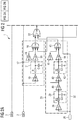
In the shown embodiment ofFig. 4 , theclock edge counter 4 comprises a ripple counter. The ripple counter shown inFig. 4 comprises four flip-flops 27-1, 27-2, 27-3, 27-4 to count detected signal edges of the received clock signal CLK to provide an incremented n-bit counter value at output terminals 28-1, 28-2, 28-3, 28-4 connected to corresponding inputs 29-1, 29-2, 29-3, 29-4 via parallel signal lines 30-1, 30-2, 30-3, 30-4 as illustrated inFig. 2 . In the shown exemplary embodiment, theclock edge counter 4 comprises four D-flip-flops and generates an incremented 4-bit counter value applied to theadjustable delay line 5 having a corresponding number of n=4 inverters being connected to each other in parallel and enabled by a corresponding bit of the n-bit counter value as also illustrated inFig. 3 . In the shown exemplary embodiment, the first bit of the ripple counter value output at terminal 28-1 has the lowest bit significance, whereas the bit output by the last serial connected D-flip-flop 27-4 output at terminal 28-4 has the highest bit significance. Each D-flip-flop 27-i of theclock edge counter 4 comprises a clock input being connected to the data output of the previous flip-flop. The data input D of each D-flip-flop 27-i is connected to the inverted data outputQ of the same flip-flop. Further, each D-flip-flop comprises a preset input PRE connected to a fixed potential and a clear input CLR connected to areset input 31 of theclock edge counter 4 as illustrated inFig. 4 . An asynchron ripple counter as shown inFig. 4 is an asynchronous counter having a first flip-flop 27-1 being clocked by the external clock signal CLK. All subsequent flip-flops 27-i are clocked by the output of the preceding flip-flop. The MOD of the ripple counter is 2n when n-flip-flops are used. For a 4-bit ripple counter, the count range of the count value is 0000 to 1111. In a possible embodiment, the counter value is incremented stepwise, wherein the count sequence does repeat itself. There are different ways to implement theripple counter 4 depending on the characteristics of the used flip-flops and the requirements of the respective count sequence. In the shown exemplary embodiment ofFig. 4 , the ripple counter is implemented by using D-flip-flops. In other embodiments, it is also possible to use different kinds of flip-flops such as JK-flip-flops. Further, it is possible to use as a clock trigger a positive edge or a negative signal edge. Further, it is possible to vary the count direction between counting up and counting down.
In the shown embodiment ofFig. 2 , the self-adjustingdelay circuit 1 has areset input terminal 26 which is connected via areset line 32 to anode 33 being connected via areset line 34 to thereset input 31 of theclock edge counter 4 and via areset line 35 to the clear inputs CLR of the D-flip-flops within theedge comparator 8 and the phasemargin security circuit 12 as illustrated inFig. 2 .
As can be seen inFig. 2 , the clockedge detector circuit 17 and thereset detector circuit 23 are both connected via theOR gate 22 to theclock input 25 of theclock edge counter 4. Theedge comparator 8 enables in the shown embodiment via the phasemargin security circuit 12 the clockedge detector circuit 17 as soon as the rising signal edge of the received data signal (data) precedes the rising signal edge of the delayed clock signal CLK' output by theadjustable delay line 5. The received data signal applied to thedata input 3 of the self-adjustingdelay circuit 1 is in a possible embodiment forwarded directly. In the embodiment shown inFig. 2 , the received data signal is forwarded via abuffer circuit 36 to adata output terminal 37 of the self-adjustingdelay circuit 1.
In the shown exemplary embodiment ofFig. 2 , thereset detector circuit 23 comprises afirst buffer circuit 38 connected via anRC delay circuit 39 to asecond buffer circuit 40 whose output is connected to the input of aninverter circuit 41 and to an output of afurther buffer circuit 42. The output of thebuffer circuit 42 is connected via a furtherRC delay circuit 43 to the input of abuffer circuit 44. The output of theinverter circuit 41 and the output of thebuffer circuit 44 are connected to corresponding inputs of an ANDgate 45 of thereset detector circuit 23. The output of the ANDgate 45 is connected with the second input of theOR gate 22 as illustrated inFig. 2 .
In the shown embodiment ofFig. 2 , the delayed clock signal CLK' output by theadjustable delay line 5 is applied via abuffer circuit 46 to aclock output terminal 47 for the delayed clock signal output by the self-adjustingdelay circuit 1.
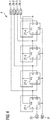
Fig. 5 shows a possible exemplary embodiment of theadjustable delay line 5 within the self-adjustingdelay circuit 1. In the shown embodiment, theadjustable delay line 5 comprises aclock input 48 connected via aclock line 49 to theclock input 2 of the self-adjustingdelay circuit 1. Accordingly, theclock input 48 receives directly the applied clock signal CLK. In the shown embodiment, theadjustable delay line 5 comprises a number of inverters 50-1, 50-2, 50-3, 50-4 being connected to each other in parallel and being enabled by a corresponding bit of the n-bit counter value received from theclock edge counter 4. As can be seen inFig. 3 , each of the parallel inverters 50-i is enabled via an internal line 51-i connected to an enabling bit input terminal 29-i of theadjustable delay line 5. Theadjustable delay line 5 further comprises an inverter 50-0 whose input is connected via aninverter 52 to theclock input 48 of theadjustable delay line 5. The inverters 50-i are connected to each other in parallel, as illustrated inFig. 3 . The inverters 50-1, 50-2, 50-3, 50-4 are enabled by an associated bit of the n-bit counter value to invert the received clock signal, wherein the driving current strength of the respective inverter does correspond to the bit-significance of the respective bit of the n-bit counter value to load acapacitor 53 of theadjustable delay line 5. In the shown exemplary embodiment, the inverter 50-1 is enabled by the bit of the counter value having the least significance (LSB) and the inverter 50-4 is enabled by the bit of the counter value having the highest or most significance (MSB). Accordingly, in the shown embodiment, the lowest significant bit LSB of the counter value enables the inverter 50-1, wherein the most significant bit MSB enables the inverter 50-4 with the highest current driving strength. In the shown exemplary embodiment, the inverter 50-1 has a current driving strength of 2°=1, the second inverter 50-2 has a current driving strength of 21=2, the third inverter 50-3 has a driving strength of 22=4 and the fourth inverter 50-4 has a driving strength of 23=8. The inverters 50-0 has in the shown exemplary embodiment a predetermined driving strength of 4 corresponding to the driving strength of theinverter 52 and corresponding to the number of bits of the n-bit counter value. In the shown embodiment, thecapacitor 53 has a predetermined capacitance of 1 pF. The time delay provided by theadjustable delay line 5 depends on the driving strength of the inverters and the capacitance C of thecapacitor 53. The outputs of the inverters 50-0 to 50-4 are all connected to acommon node 54. Thecapacitor 53 is connected between thecommon node 54 and anode 55 at a predetermined potential as illustrated inFig. 3 . In the shown exemplary embodiment,node 54 is connected via two serial connectedbuffer circuits clock output 58 of theadjustable delay line 5 supplying a delayed clock signal CLK' via thebuffer circuit 46 to theoutput clock terminal 57 of the self-adjustingdelay circuit 1. Further, the delayed clock signal CLK' is applied via the clock line 6 to theedge detector circuit 8 and the phasemargin security circuit 12. -
Fig. 5 shows a circuit diagram of an exemplary embodiment of a three-state inverter which can be used in theadjustable delay line 5 for the inverter circuits 50-1, 50-2, 50-3, 50-4. As can be seen inFig. 5 , each three-state inverter 50-i comprises asignal input 59 and an enablecontrol input 60. Thesignal input 59 is connected within theadjustable delay line 5 via a corresponding internal line 61 to acommon node 62 to receive the inverted clock signal. The enablecontrol input 60 is connected via internal control lines 51-1, 51-i to a corresponding control input 29-i of theadjustable delay line 5. The three-state inverter 50-i comprises aninternal inverter 63 connected to the gate of a PMOS M3. The enablecontrol input 60 is connected via theinternal inverter 63 to the control gate of the PMOS M3 and directly via aninternal line 64 to the gate of an NMOS M4. Thesignal input 59 connected to thenode 62 is applied to the gate of a PMOS M1 and to the gate of a complementary NMOS M2 as illustrated inFig. 5 . The three-state inverter 50-i illustrated inFig. 5 , inverts the received signal applied to thesignal input 59 with a predetermined current strength of theinternal inverter 63, if the enablecontrol input 60 receives an enabling signal, i.e. a bit of the n-bit counter value. Theoutput 65 of the three-state inverter 50-i is connected tonode 54 of theadjustable delay line 5 shown inFig. 3 .
The self-adjustingdelay circuit 1, as shown in the embodiment ofFig. 2 comprises four main sub-blocks including theadjustable delay line 5, theclock edge counter 4, the clockedge detector circuit 17 and the phasemargin security circuit 12 which secures a predetermined phase or time margin. Theclock edge counter 4 in the embodiment shown inFig. 2 comprises a 4-bit counter, but it can be in different embodiments of different size depending on the desired precision. The number of the counter bits of the n-bit counter value defines a correction step size, step number and correction range. The phasemargin security circuit 12 secures the phase margin comprising in the shown embodiment ofFig. 2 three flip-flops, but their number can be increased as well depending on the requirements for a set-up time. Theedge comparator 8 can use the same type of flip-flops as the phasemargin security circuit 12. Some additional logic is used to adjust delays for the signal. In a possible embodiment, these logic blocks can be placed in the input pads. All other sub-blocks of the self-adjustingdelay circuit 1 can be placed in a possible embodiment close to the shift register or latch for which these inputs form the signal shape.
At a power-up sequence, a reset of all flip-flops is done. On outputs 28-i of the clock edge counter 4 a low bit value "0" is provided. The falling edge of the POR (Power on Reset) signal by use of the falling edge detector creates a short pulse which through theOR gate 22 is applied to theclock input 25 of theclock edge counter 4. Thus, after the POR signal has been generated, all flip-flops are set to a logical high value "1" at their outputs. In this way, all three-state inverters 50-i of theadjustable delay line 5 are enabled and the resulting delay of theadjustable delay line 5 is small. For adjusting the delay of the self-adjusting delay line after the start-up, a sequence of RZ (Return Zero) only "1" is applied at the data input. This data is also applied to the data input of the edge detector. The clock signal CLK' delayed by theadjustable delay line 5 is applied to the clock input 7 of theedge comparator 8. If the set-up time is not enough, theedge comparator 8 samples a logical low value "0". The following clock period causes a change in the counter status. It enables an inverter with a lower driving capability and disables one with a higher driving capability so that the total strength of the parallel connected three-state inverters is reduced slightly and the delay of theadjustable delay line 5 increases. Theedge comparator 8 comprising the D-flip-flop 9 is clocked now with a slightly more delayed clock signal. If the set-up time is still not enough, this process is repeated until the set-up time becomes sufficient to trigger the flip-flop 9 of theedge comparator 8. The logical high value "1" which does appear on its output is sampled by the phasemargin security circuit 12. After two clock periods, the sampled signal appears at the circuitry output of thephase margin circuit 12. The inverted signal gates further the clock signal for theclock edge counter 4 which keeps its state until the power-down of the chip. A few additional delay steps create a security margin needed because of the noise and the possible clock jitter of the clock signal. In case that two clock periods (two adjustment steps) are not provided with enough security margin, it is possible to add further flip-flops in a pipeline within the phasemargin security circuit 12. To achieve the desired phase margin, each flip-flop can add one adjustment step to the margin (4-bit counter in the self-adjustingdelay line 5 corresponds to 16 adjustment steps).
When the self-adjustment process stops (with enough phase margin for the set-up time), the gated clock signal stops at the input of theclock edge counter 4 and thus remains in this status keeping theadjustable delay line 5 adjusted with the necessary fitting time delay. It is possible that the value is recorded in the counter giving an optimal delay time. This optimal delay time can be written in an OTP (One Time Programmable) to program theadjustable delay line 5. -
Fig. 6 shows signal diagrams for illustrating the operation of a self-adjustingdelay circuit 1 according to the present invention as illustrated inFig. 2 .Fig. 6A shows the power on reset (POR) signal making a short pulse which through theOR gate 22 is applied to theclock input 25 of theclock edge counter 4.Figs. 6B, 6C, 6D, 6E illustrate different counter output bits of a 4-bitclock edge counter 4, as shown in the embodiment ofFig. 2 .Fig. 6F illustrates the counter input signal.Fig. 6H shows the margin generation output by the phasemargin security circuit 12 of the self-adjustingdelay circuit 1.Fig. 6I shows the SADL edge detector output of theedge comparator 8.Fig. 6J illustrates input data andFig. 6K illustrates a corresponding input clock signal.
With the self-adjustingdelay circuit 1 according to the present invention it is possible that the time delay of theadjustable delay line 5 is adjusted for different technology process parameters. Moreover, the delay of the delay line can be adjusted for different power supply voltages. The adjustment of the delay guarantees that each received data packet or data can be sampled correctly. The power consumption of the self-adjustingdelay circuit 1 after adjustment is equal to a conventional RC-delay line. Accordingly, no additional power is required and the self-adjustingdelay circuit 1 does not consume more electrical power than conventional delay lines. The self-adjustingdelay circuit 1 according to the present invention can handle process variations and parasitic elements caused by the circuit design. Whereas conventional delay lines are hard-wired and cannot be adapted, the delay circuit according to the present invention is self-adjusting. The self-adjustingdelay circuit 1 according to the present invention can be used in any circuits to delay a clock signal guaranteeing in this way a set-up time independently on the power supply range and the technology parameter variations.
Claims (12)
- A self-adjusting delay circuit (1) adapted to delay a received clock signal (CLK) provided for a received data signal (data),
said self-adjusting delay circuit (1) comprising:a clock edge counter (4) adapted to count signal edges of the received clock signal (CLK) providing an incremented n-bit counter value at output terminals (28-i) connected to corresponding inputs (29-i) of an adjustable delay line (5) of said self-adjusting delay circuit (1) via parallel signal lines (30-i), said adjustable delay line (5) having a number (n) of inverters (50-i) being connected to each other in parallel,wherein each inverter (50-i) of said adjustable delay line (5) is enabled by an associated bit of the n-bit counter value received from said clock edge counter (4) via the parallel signal lines (30-i) to invert the received clock signal (CLK) with a driving current strength of the inverter (50-i) corresponding to the significance of the respective bit of said n-bit counter value to load a capacitor (53) of said adjustable delay line (5) connected to the outputs of the inverters (50-i),wherein the driving current strength of the i-th inverter (50-i) of said adjustable delay line (5) is 2i-1 with 1≤i≤n, said self-adjusting delay circuit (1) further comprising:- an edge comparator (8) formed by a flip-flop (9) having a clock input (7) receiving the delayed clock signal (CLK') output by a clock output (58) of said adjustable delay line (5) and having a data input (10) receiving the data signal (data) and- a phase margin security circuit (12) for providing a phase margin security against clock jitter of the received clock signal (CLK), said phase margin security circuit (12) comprising a predetermined number of flip-flops (13-i) connected in series to each other,wherein the first flip-flop (13-1) of said phase margin security circuit (12) is connected to an output (11) of the flip-flop (9) of said edge comparator (8),wherein the received clock signal (CLK) is delayed by said adjustable delay line (5) with an increasing time delay proportional to the incremented n-bit counter value output by said clock edge counter (4) until said edge comparator (8) detects that a rising signal edge of the received data signal (data) precedes a rising signal edge of the delayed clock signal (CLK') output by the clock output (58) of said adjustable delay line (5) including a time margin provided by said phase margin security circuit (12). - The self-adjusting delay circuit according to claim 1,
wherein the clock edge counter (4) is a ripple counter comprising a predetermined number (n) of flip-flops (27-i) connected in series to each other. - The self-adjusting delay circuit according to claim 1 or 2,
wherein the inverters (50-1, 50-2, 50-3, 50-4) of the adjustable delay line (5) are three-state inverters each being enabled by a bit of the n-bit counter value output by said clock edge counter (4) adapter to invert the received clock signal (CLK) with a driving current strength corresponding to the significance of the respective enabling bit. - The self-adjusting delay circuit according to one of the preceding claims 1 to 3, comprising
a reset detector circuit (23) adapted to generate in response to a reset signal (RST) a single pulse to set flip-flops of said clock edge counter (4). - The self-adjusting delay circuit according to one of the preceding claims 1 to 4, comprising
a clock edge detector circuit (17) adapted to detect falling signal edges of the received clock signal (CLK). - The self-adjusting delay circuit according to claim 5 when dependent on claim 4, wherein the reset detector circuit (23) and the clock edge detector circuit (17) are connected via an OR gate (22) to a clock input (25) of said clock edge counter (4).
- The self-adjusting delay circuit according to one of the preceding claims 1 to 6,
wherein the output (11) of said edge comparator (8) is set if the rising signal edge of the received data signal (data) appears before a rising signal edge of the delayed clock signal (CLK') output by the adjustable delay line (5) . - The self-adjusting delay circuit according to one of the preceding claims 5 to 6, or according to claim 7 when dependent on one of the claims 5 to 6, wherein said edge comparator (8) is adapted to disable directly or via said phase margin security circuit (12) the clock edge detector circuit (17) as soon as the rising signal edge of the received data signal precedes the rising signal edge of the delayed clock signal (CLK') output by said adjustable delay line (5).
- The self-adjusting delay circuit according to one of the preceding claims 1 to 8,
wherein the received data signal (data) is forwarded directly or via a buffer circuit (36) of said self-adjusting delay circuit (1). - The self-adjusting delay circuit according to one of the preceding claims 1 to 9,
wherein said clock edge counter (4), said edge comparator (8) and said phase margin security circuit (12) comprise the same type of flip-flops. - The self-adjusting delay circuit according to claim 10,
wherein the flip-flops of said clock edge counter (4), said edge comparator (8) and said phase margin security circuit (12) comprise D-flip-flops. - A delay locked loop (DLL) circuit comprising a self-adjusting delay circuit (1) according to one of the preceding claims 1 to 11.
Priority Applications (1)
| Application Number | Priority Date | Filing Date | Title |
|---|---|---|---|
| EP13197006.3A EP2884366B1 (en) | 2013-12-12 | 2013-12-12 | Self-adjusting delay circuit |
Applications Claiming Priority (1)
| Application Number | Priority Date | Filing Date | Title |
|---|---|---|---|
| EP13197006.3A EP2884366B1 (en) | 2013-12-12 | 2013-12-12 | Self-adjusting delay circuit |
Publications (2)
| Publication Number | Publication Date |
|---|---|
| EP2884366A1 EP2884366A1 (en) | 2015-06-17 |
| EP2884366B1 true EP2884366B1 (en) | 2018-10-10 |
Family
ID=49919991
Family Applications (1)
| Application Number | Title | Priority Date | Filing Date |
|---|---|---|---|
| EP13197006.3A Not-in-force EP2884366B1 (en) | 2013-12-12 | 2013-12-12 | Self-adjusting delay circuit |
Country Status (1)
| Country | Link |
|---|---|
| EP (1) | EP2884366B1 (en) |
Families Citing this family (3)
| Publication number | Priority date | Publication date | Assignee | Title |
|---|---|---|---|---|
| TWI623198B (en) * | 2016-10-20 | 2018-05-01 | 國立高雄第一科技大學 | Resolution-enhancing cmos full-digital-structurally pulse mixing method and device thereof |
| US10333532B2 (en) | 2017-09-07 | 2019-06-25 | Micron Technology, Inc. | Apparatuses and methods for detecting a loop count in a delay-locked loop |
| CN114944834B (en) * | 2022-06-13 | 2024-12-31 | 浙江大学 | A low power consumption clock amplifier circuit |
Family Cites Families (5)
| Publication number | Priority date | Publication date | Assignee | Title |
|---|---|---|---|---|
| GB2359706B (en) * | 2000-02-28 | 2004-03-10 | Mitel Corp | Integrated data clock extractor |
| JP2001326563A (en) * | 2000-05-18 | 2001-11-22 | Mitsubishi Electric Corp | DLL circuit |
| KR100493046B1 (en) * | 2003-02-04 | 2005-06-07 | 삼성전자주식회사 | Frequency multiplier of clock capable of adjusting duty cycle of the clock and method thereof |
| US7057435B2 (en) * | 2003-05-30 | 2006-06-06 | Regents Of The University Of California | Distributed delay-locked-based clock and data recovery systems |
| US8618857B2 (en) * | 2012-03-27 | 2013-12-31 | Monolithic Power Systems, Inc. | Delay circuit and associated method |
-
2013
- 2013-12-12 EP EP13197006.3A patent/EP2884366B1/en not_active Not-in-force
Non-Patent Citations (1)
| Title |
|---|
| None * |
Also Published As
| Publication number | Publication date |
|---|---|
| EP2884366A1 (en) | 2015-06-17 |
Similar Documents
| Publication | Publication Date | Title |
|---|---|---|
| US7839194B2 (en) | Clock circuitry for generating multiple clocks with time-multiplexed duty cycle adjustment | |
| KR100362199B1 (en) | A register controlled DLL using ring delay and counter | |
| US8416001B2 (en) | Techniques for reducing duty cycle distortion in periodic signals | |
| US9337817B2 (en) | Hold-time optimization circuit and receiver with the same | |
| TWI442704B (en) | An apparatus for counting input pulses during a specific time interval | |
| CN113841334A (en) | Measurement and correction of multiphase clock duty cycle and time offset | |
| US7924963B2 (en) | Digital Transmit phase trimming | |
| US7071751B1 (en) | Counter-controlled delay line | |
| US7234069B1 (en) | Precise phase shifting using a DLL controlled, multi-stage delay chain | |
| US7457191B2 (en) | Apparatus and method of generating output enable signal for semiconductor memory apparatus | |
| US9203605B2 (en) | CMOS interpolator for a serializer/deserializer communication application | |
| CN104793918A (en) | Deterministic fifo buffer | |
| CN104639157A (en) | Timing adjustment circuit and semiconductor integrated circuit device | |
| US11770116B1 (en) | Duty cycle correction for high-speed clock signals | |
| US7231536B1 (en) | Control circuit for self-compensating delay chain for multiple-data-rate interfaces | |
| Schell et al. | A low power tunable delay element suitable for asynchronous delays of burst information | |
| EP2884366B1 (en) | Self-adjusting delay circuit | |
| US20050285648A1 (en) | Closed-loop independent DLL-controlled rise/fall time control circuit | |
| US8824616B1 (en) | CMOS interpolator for a serializer/deserializer communication application | |
| US7042267B1 (en) | Gated clock circuit with a substantially increased control signal delay | |
| CN101110582B (en) | delay control circuit | |
| JP3945894B2 (en) | Semiconductor device and signal input state detection circuit | |
| KR20200145266A (en) | Phase detection circuit, clock generation circuit and semiconductor apparatus using the same | |
| CN113381750A (en) | Circulation borrowing counter | |
| KR100321732B1 (en) | Delay Locked Loop using Digital Ring Synchronous Mirror Delay |
Legal Events
| Date | Code | Title | Description |
|---|---|---|---|
| PUAI | Public reference made under article 153(3) epc to a published international application that has entered the european phase |
Free format text: ORIGINAL CODE: 0009012 |
|
| 17P | Request for examination filed |
Effective date: 20131212 |
|
| AK | Designated contracting states |
Kind code of ref document: A1 Designated state(s): AL AT BE BG CH CY CZ DE DK EE ES FI FR GB GR HR HU IE IS IT LI LT LU LV MC MK MT NL NO PL PT RO RS SE SI SK SM TR |
|
| AX | Request for extension of the european patent |
Extension state: BA ME |
|
| R17P | Request for examination filed (corrected) |
Effective date: 20151216 |
|
| RBV | Designated contracting states (corrected) |
Designated state(s): AL AT BE BG CH CY CZ DE DK EE ES FI FR GB GR HR HU IE IS IT LI LT LU LV MC MK MT NL NO PL PT RO RS SE SI SK SM TR |
|
| GRAP | Despatch of communication of intention to grant a patent |
Free format text: ORIGINAL CODE: EPIDOSNIGR1 |
|
| STAA | Information on the status of an ep patent application or granted ep patent |
Free format text: STATUS: GRANT OF PATENT IS INTENDED |
|
| RIC1 | Information provided on ipc code assigned before grant |
Ipc: G06F 1/12 20060101ALI20180425BHEP Ipc: H03L 7/081 20060101ALI20180425BHEP Ipc: G06F 1/04 20060101AFI20180425BHEP Ipc: H04L 7/00 20060101ALI20180425BHEP Ipc: H03K 5/131 20140101ALI20180425BHEP |
|
| INTG | Intention to grant announced |
Effective date: 20180516 |
|
| RAP1 | Party data changed (applicant data changed or rights of an application transferred) |
Owner name: ROHM CO., LTD. |
|
| GRAS | Grant fee paid |
Free format text: ORIGINAL CODE: EPIDOSNIGR3 |
|
| GRAA | (expected) grant |
Free format text: ORIGINAL CODE: 0009210 |
|
| STAA | Information on the status of an ep patent application or granted ep patent |
Free format text: STATUS: THE PATENT HAS BEEN GRANTED |
|
| AK | Designated contracting states |
Kind code of ref document: B1 Designated state(s): AL AT BE BG CH CY CZ DE DK EE ES FI FR GB GR HR HU IE IS IT LI LT LU LV MC MK MT NL NO PL PT RO RS SE SI SK SM TR |
|
| REG | Reference to a national code |
Ref country code: GB Ref legal event code: FG4D |
|
| REG | Reference to a national code |
Ref country code: CH Ref legal event code: EP Ref country code: AT Ref legal event code: REF Ref document number: 1051988 Country of ref document: AT Kind code of ref document: T Effective date: 20181015 |
|
| REG | Reference to a national code |
Ref country code: IE Ref legal event code: FG4D |
|
| REG | Reference to a national code |
Ref country code: DE Ref legal event code: R096 Ref document number: 602013044791 Country of ref document: DE |
|
| REG | Reference to a national code |
Ref country code: NL Ref legal event code: MP Effective date: 20181010 |
|
| REG | Reference to a national code |
Ref country code: LT Ref legal event code: MG4D |
|
| REG | Reference to a national code |
Ref country code: AT Ref legal event code: MK05 Ref document number: 1051988 Country of ref document: AT Kind code of ref document: T Effective date: 20181010 |
|
| PG25 | Lapsed in a contracting state [announced via postgrant information from national office to epo] |
Ref country code: NL Free format text: LAPSE BECAUSE OF FAILURE TO SUBMIT A TRANSLATION OF THE DESCRIPTION OR TO PAY THE FEE WITHIN THE PRESCRIBED TIME-LIMIT Effective date: 20181010 |
|
| PG25 | Lapsed in a contracting state [announced via postgrant information from national office to epo] |
Ref country code: BG Free format text: LAPSE BECAUSE OF FAILURE TO SUBMIT A TRANSLATION OF THE DESCRIPTION OR TO PAY THE FEE WITHIN THE PRESCRIBED TIME-LIMIT Effective date: 20190110 Ref country code: IS Free format text: LAPSE BECAUSE OF FAILURE TO SUBMIT A TRANSLATION OF THE DESCRIPTION OR TO PAY THE FEE WITHIN THE PRESCRIBED TIME-LIMIT Effective date: 20190210 Ref country code: NO Free format text: LAPSE BECAUSE OF FAILURE TO SUBMIT A TRANSLATION OF THE DESCRIPTION OR TO PAY THE FEE WITHIN THE PRESCRIBED TIME-LIMIT Effective date: 20190110 Ref country code: AT Free format text: LAPSE BECAUSE OF FAILURE TO SUBMIT A TRANSLATION OF THE DESCRIPTION OR TO PAY THE FEE WITHIN THE PRESCRIBED TIME-LIMIT Effective date: 20181010 Ref country code: FI Free format text: LAPSE BECAUSE OF FAILURE TO SUBMIT A TRANSLATION OF THE DESCRIPTION OR TO PAY THE FEE WITHIN THE PRESCRIBED TIME-LIMIT Effective date: 20181010 Ref country code: LV Free format text: LAPSE BECAUSE OF FAILURE TO SUBMIT A TRANSLATION OF THE DESCRIPTION OR TO PAY THE FEE WITHIN THE PRESCRIBED TIME-LIMIT Effective date: 20181010 Ref country code: HR Free format text: LAPSE BECAUSE OF FAILURE TO SUBMIT A TRANSLATION OF THE DESCRIPTION OR TO PAY THE FEE WITHIN THE PRESCRIBED TIME-LIMIT Effective date: 20181010 Ref country code: PL Free format text: LAPSE BECAUSE OF FAILURE TO SUBMIT A TRANSLATION OF THE DESCRIPTION OR TO PAY THE FEE WITHIN THE PRESCRIBED TIME-LIMIT Effective date: 20181010 Ref country code: ES Free format text: LAPSE BECAUSE OF FAILURE TO SUBMIT A TRANSLATION OF THE DESCRIPTION OR TO PAY THE FEE WITHIN THE PRESCRIBED TIME-LIMIT Effective date: 20181010 Ref country code: LT Free format text: LAPSE BECAUSE OF FAILURE TO SUBMIT A TRANSLATION OF THE DESCRIPTION OR TO PAY THE FEE WITHIN THE PRESCRIBED TIME-LIMIT Effective date: 20181010 |
|
| PG25 | Lapsed in a contracting state [announced via postgrant information from national office to epo] |
Ref country code: PT Free format text: LAPSE BECAUSE OF FAILURE TO SUBMIT A TRANSLATION OF THE DESCRIPTION OR TO PAY THE FEE WITHIN THE PRESCRIBED TIME-LIMIT Effective date: 20190210 Ref country code: SE Free format text: LAPSE BECAUSE OF FAILURE TO SUBMIT A TRANSLATION OF THE DESCRIPTION OR TO PAY THE FEE WITHIN THE PRESCRIBED TIME-LIMIT Effective date: 20181010 Ref country code: GR Free format text: LAPSE BECAUSE OF FAILURE TO SUBMIT A TRANSLATION OF THE DESCRIPTION OR TO PAY THE FEE WITHIN THE PRESCRIBED TIME-LIMIT Effective date: 20190111 Ref country code: AL Free format text: LAPSE BECAUSE OF FAILURE TO SUBMIT A TRANSLATION OF THE DESCRIPTION OR TO PAY THE FEE WITHIN THE PRESCRIBED TIME-LIMIT Effective date: 20181010 Ref country code: RS Free format text: LAPSE BECAUSE OF FAILURE TO SUBMIT A TRANSLATION OF THE DESCRIPTION OR TO PAY THE FEE WITHIN THE PRESCRIBED TIME-LIMIT Effective date: 20181010 |
|
| REG | Reference to a national code |
Ref country code: DE Ref legal event code: R097 Ref document number: 602013044791 Country of ref document: DE |
|
| PG25 | Lapsed in a contracting state [announced via postgrant information from national office to epo] |
Ref country code: CZ Free format text: LAPSE BECAUSE OF FAILURE TO SUBMIT A TRANSLATION OF THE DESCRIPTION OR TO PAY THE FEE WITHIN THE PRESCRIBED TIME-LIMIT Effective date: 20181010 Ref country code: DK Free format text: LAPSE BECAUSE OF FAILURE TO SUBMIT A TRANSLATION OF THE DESCRIPTION OR TO PAY THE FEE WITHIN THE PRESCRIBED TIME-LIMIT Effective date: 20181010 Ref country code: IT Free format text: LAPSE BECAUSE OF FAILURE TO SUBMIT A TRANSLATION OF THE DESCRIPTION OR TO PAY THE FEE WITHIN THE PRESCRIBED TIME-LIMIT Effective date: 20181010 |
|
| REG | Reference to a national code |
Ref country code: CH Ref legal event code: PL |
|
| PLBE | No opposition filed within time limit |
Free format text: ORIGINAL CODE: 0009261 |
|
| STAA | Information on the status of an ep patent application or granted ep patent |
Free format text: STATUS: NO OPPOSITION FILED WITHIN TIME LIMIT |
|
| PG25 | Lapsed in a contracting state [announced via postgrant information from national office to epo] |
Ref country code: LU Free format text: LAPSE BECAUSE OF NON-PAYMENT OF DUE FEES Effective date: 20181212 Ref country code: MC Free format text: LAPSE BECAUSE OF FAILURE TO SUBMIT A TRANSLATION OF THE DESCRIPTION OR TO PAY THE FEE WITHIN THE PRESCRIBED TIME-LIMIT Effective date: 20181010 Ref country code: EE Free format text: LAPSE BECAUSE OF FAILURE TO SUBMIT A TRANSLATION OF THE DESCRIPTION OR TO PAY THE FEE WITHIN THE PRESCRIBED TIME-LIMIT Effective date: 20181010 Ref country code: SM Free format text: LAPSE BECAUSE OF FAILURE TO SUBMIT A TRANSLATION OF THE DESCRIPTION OR TO PAY THE FEE WITHIN THE PRESCRIBED TIME-LIMIT Effective date: 20181010 Ref country code: RO Free format text: LAPSE BECAUSE OF FAILURE TO SUBMIT A TRANSLATION OF THE DESCRIPTION OR TO PAY THE FEE WITHIN THE PRESCRIBED TIME-LIMIT Effective date: 20181010 Ref country code: SK Free format text: LAPSE BECAUSE OF FAILURE TO SUBMIT A TRANSLATION OF THE DESCRIPTION OR TO PAY THE FEE WITHIN THE PRESCRIBED TIME-LIMIT Effective date: 20181010 |
|
| 26N | No opposition filed |
Effective date: 20190711 |
|
| REG | Reference to a national code |
Ref country code: IE Ref legal event code: MM4A |
|
| GBPC | Gb: european patent ceased through non-payment of renewal fee |
Effective date: 20190110 |
|
| REG | Reference to a national code |
Ref country code: BE Ref legal event code: MM Effective date: 20181231 |
|
| PG25 | Lapsed in a contracting state [announced via postgrant information from national office to epo] |
Ref country code: IE Free format text: LAPSE BECAUSE OF NON-PAYMENT OF DUE FEES Effective date: 20181212 Ref country code: FR Free format text: LAPSE BECAUSE OF NON-PAYMENT OF DUE FEES Effective date: 20181231 Ref country code: SI Free format text: LAPSE BECAUSE OF FAILURE TO SUBMIT A TRANSLATION OF THE DESCRIPTION OR TO PAY THE FEE WITHIN THE PRESCRIBED TIME-LIMIT Effective date: 20181010 |
|
| PG25 | Lapsed in a contracting state [announced via postgrant information from national office to epo] |
Ref country code: BE Free format text: LAPSE BECAUSE OF NON-PAYMENT OF DUE FEES Effective date: 20181231 |
|
| PG25 | Lapsed in a contracting state [announced via postgrant information from national office to epo] |
Ref country code: CH Free format text: LAPSE BECAUSE OF NON-PAYMENT OF DUE FEES Effective date: 20181231 Ref country code: LI Free format text: LAPSE BECAUSE OF NON-PAYMENT OF DUE FEES Effective date: 20181231 Ref country code: GB Free format text: LAPSE BECAUSE OF NON-PAYMENT OF DUE FEES Effective date: 20190110 |
|
| PG25 | Lapsed in a contracting state [announced via postgrant information from national office to epo] |
Ref country code: MT Free format text: LAPSE BECAUSE OF NON-PAYMENT OF DUE FEES Effective date: 20181212 |
|
| PG25 | Lapsed in a contracting state [announced via postgrant information from national office to epo] |
Ref country code: TR Free format text: LAPSE BECAUSE OF FAILURE TO SUBMIT A TRANSLATION OF THE DESCRIPTION OR TO PAY THE FEE WITHIN THE PRESCRIBED TIME-LIMIT Effective date: 20181010 |
|
| PG25 | Lapsed in a contracting state [announced via postgrant information from national office to epo] |
Ref country code: HU Free format text: LAPSE BECAUSE OF FAILURE TO SUBMIT A TRANSLATION OF THE DESCRIPTION OR TO PAY THE FEE WITHIN THE PRESCRIBED TIME-LIMIT; INVALID AB INITIO Effective date: 20131212 Ref country code: CY Free format text: LAPSE BECAUSE OF FAILURE TO SUBMIT A TRANSLATION OF THE DESCRIPTION OR TO PAY THE FEE WITHIN THE PRESCRIBED TIME-LIMIT Effective date: 20181010 Ref country code: MK Free format text: LAPSE BECAUSE OF NON-PAYMENT OF DUE FEES Effective date: 20181010 |
|
| PGFP | Annual fee paid to national office [announced via postgrant information from national office to epo] |
Ref country code: DE Payment date: 20211102 Year of fee payment: 9 |
|
| REG | Reference to a national code |
Ref country code: DE Ref legal event code: R119 Ref document number: 602013044791 Country of ref document: DE |
|
| PG25 | Lapsed in a contracting state [announced via postgrant information from national office to epo] |
Ref country code: DE Free format text: LAPSE BECAUSE OF NON-PAYMENT OF DUE FEES Effective date: 20230701 |