EP2881656A1 - Backlight module, display device and method for reducing bright spot phenomenon - Google Patents
Backlight module, display device and method for reducing bright spot phenomenon Download PDFInfo
- Publication number
- EP2881656A1 EP2881656A1 EP12852438.6A EP12852438A EP2881656A1 EP 2881656 A1 EP2881656 A1 EP 2881656A1 EP 12852438 A EP12852438 A EP 12852438A EP 2881656 A1 EP2881656 A1 EP 2881656A1
- Authority
- EP
- European Patent Office
- Prior art keywords
- light
- backlight module
- guide plate
- indents
- optical film
- Prior art date
- Legal status (The legal status is an assumption and is not a legal conclusion. Google has not performed a legal analysis and makes no representation as to the accuracy of the status listed.)
- Granted
Links
Images

Classifications
-
- G—PHYSICS
- G02—OPTICS
- G02B—OPTICAL ELEMENTS, SYSTEMS OR APPARATUS
- G02B6/00—Light guides; Structural details of arrangements comprising light guides and other optical elements, e.g. couplings
- G02B6/0001—Light guides; Structural details of arrangements comprising light guides and other optical elements, e.g. couplings specially adapted for lighting devices or systems
- G02B6/0011—Light guides; Structural details of arrangements comprising light guides and other optical elements, e.g. couplings specially adapted for lighting devices or systems the light guides being planar or of plate-like form
-
- G—PHYSICS
- G02—OPTICS
- G02B—OPTICAL ELEMENTS, SYSTEMS OR APPARATUS
- G02B6/00—Light guides; Structural details of arrangements comprising light guides and other optical elements, e.g. couplings
- G02B6/0001—Light guides; Structural details of arrangements comprising light guides and other optical elements, e.g. couplings specially adapted for lighting devices or systems
- G02B6/0011—Light guides; Structural details of arrangements comprising light guides and other optical elements, e.g. couplings specially adapted for lighting devices or systems the light guides being planar or of plate-like form
- G02B6/0013—Means for improving the coupling-in of light from the light source into the light guide
- G02B6/0015—Means for improving the coupling-in of light from the light source into the light guide provided on the surface of the light guide or in the bulk of it
- G02B6/002—Means for improving the coupling-in of light from the light source into the light guide provided on the surface of the light guide or in the bulk of it by shaping at least a portion of the light guide, e.g. with collimating, focussing or diverging surfaces
-
- F—MECHANICAL ENGINEERING; LIGHTING; HEATING; WEAPONS; BLASTING
- F21—LIGHTING
- F21K—NON-ELECTRIC LIGHT SOURCES USING LUMINESCENCE; LIGHT SOURCES USING ELECTROCHEMILUMINESCENCE; LIGHT SOURCES USING CHARGES OF COMBUSTIBLE MATERIAL; LIGHT SOURCES USING SEMICONDUCTOR DEVICES AS LIGHT-GENERATING ELEMENTS; LIGHT SOURCES NOT OTHERWISE PROVIDED FOR
- F21K9/00—Light sources using semiconductor devices as light-generating elements, e.g. using light-emitting diodes [LED] or lasers
- F21K9/60—Optical arrangements integrated in the light source, e.g. for improving the colour rendering index or the light extraction
- F21K9/61—Optical arrangements integrated in the light source, e.g. for improving the colour rendering index or the light extraction using light guides
-
- G—PHYSICS
- G02—OPTICS
- G02F—OPTICAL DEVICES OR ARRANGEMENTS FOR THE CONTROL OF LIGHT BY MODIFICATION OF THE OPTICAL PROPERTIES OF THE MEDIA OF THE ELEMENTS INVOLVED THEREIN; NON-LINEAR OPTICS; FREQUENCY-CHANGING OF LIGHT; OPTICAL LOGIC ELEMENTS; OPTICAL ANALOGUE/DIGITAL CONVERTERS
- G02F1/00—Devices or arrangements for the control of the intensity, colour, phase, polarisation or direction of light arriving from an independent light source, e.g. switching, gating or modulating; Non-linear optics
- G02F1/01—Devices or arrangements for the control of the intensity, colour, phase, polarisation or direction of light arriving from an independent light source, e.g. switching, gating or modulating; Non-linear optics for the control of the intensity, phase, polarisation or colour
- G02F1/13—Devices or arrangements for the control of the intensity, colour, phase, polarisation or direction of light arriving from an independent light source, e.g. switching, gating or modulating; Non-linear optics for the control of the intensity, phase, polarisation or colour based on liquid crystals, e.g. single liquid crystal display cells
- G02F1/133—Constructional arrangements; Operation of liquid crystal cells; Circuit arrangements
- G02F1/1333—Constructional arrangements; Manufacturing methods
- G02F1/1335—Structural association of cells with optical devices, e.g. polarisers or reflectors
- G02F1/1336—Illuminating devices
- G02F1/133615—Edge-illuminating devices, i.e. illuminating from the side
-
- G—PHYSICS
- G02—OPTICS
- G02B—OPTICAL ELEMENTS, SYSTEMS OR APPARATUS
- G02B6/00—Light guides; Structural details of arrangements comprising light guides and other optical elements, e.g. couplings
- G02B6/0001—Light guides; Structural details of arrangements comprising light guides and other optical elements, e.g. couplings specially adapted for lighting devices or systems
- G02B6/0011—Light guides; Structural details of arrangements comprising light guides and other optical elements, e.g. couplings specially adapted for lighting devices or systems the light guides being planar or of plate-like form
- G02B6/0066—Light guides; Structural details of arrangements comprising light guides and other optical elements, e.g. couplings specially adapted for lighting devices or systems the light guides being planar or of plate-like form characterised by the light source being coupled to the light guide
- G02B6/0068—Arrangements of plural sources, e.g. multi-colour light sources
Definitions
- Embodiments of the present invention relate to a backlight module, a display device and a method for eliminating hotspot effect.
- a conventional side-illuminating liquid crystal display device comprises a backlight module of the configuration as shown in Fig.1 .
- the backlight module comprises a light-guide plate 102, an optical film 103 provided on a side of the light emitting face 102b of the light-guide plate 102, and LED bar 101 provided on a side of the light incident face 102a of the light-guide plate 102.
- the LED bar 101 comprises several LEDs 101a disposed at the side thereof facing the light-guide plate 102, the light emitted from the LEDs 101a enters the light-guide plate 102 through the light incident face 102 of the light-guide plate 102 and then is guided to the optical film 103.
- the LEDs 101 usually are distributed separately along the length direction of the LED bar 101, hotspots causing uneven shade readily appears at the edge of the light-guide plate 102 adjacent to the light incident face 102a.
- the hotspots will spread from the non-displaying area to the displaying area of the display device, and then influence the display effect in the displaying area.
- hotspot phenomenon occurs, it's generally required to regulate the grid point design of the light-guide plate, return the light-guide plate to its supplier for regulation, and the regulation period is relatively long, and the regulated effect is not good.
- Embodiments of the present invention provide a backlight module, a display device and a method for eliminating the hotspot effect, to quickly and effectively eliminate the hotspot effect.
- a first aspect of the present invention provides a side-illuminating backlight module, comprising light-guide plate, an optical film attaching to a side of a light emitting face of the light-guide plate, and a strip-like assembly of point light source disposed at the side of the light incident face of the light-guide plate; the strip-like assembly of point light source comprises point light sources toward the light incident face of the light-guide plate thereon, an edge of one side of the optical film corresponding to the light incident face of the light-guide plate is provided with indents.
- the point light sources may be LEDs
- the strip-like assembly of point light source may be an LED bar.
- the indents may correspond to the point light sources in position.
- the shape of the indents may be part of an oval.
- a second aspect of the present invention further provides a display device comprising the above mentioned backlight module.
- the indents of the optical film may be located outside of a displaying area of the display device.
- a third aspect of the present invention provides a method for eliminating hotspots of a backlight module, the backlight module comprising a light-guide plate, an optical film attaching to a side of a light emitting face of the light-guide plate, and a strip-like assembly of point light source positioned at the side of the light incident face of the light-guide plate, the strip-like assembly of point light source comprises point light sources toward the light incident face of the light-guide plate thereon, and the method comprises the following steps:
- the method may further comprise, between step S1 and S3, step S2 of optimizing the shape of the indents to be formed for the optical film of the backlight module.
- the step S2 may comprise:
- the backlight module provided in an embodiment of the present invention makes the incident light distributed evenly by providing indents for the optical film of the backlight module so as to effectively and quickly eliminate the hotspot effect of the backlight module.
- the display device provided in an embodiment of the present invention, by using the above described backlight module, and makes it not easy for hotspot effect to occur or the extent of hotspot effect relatively gentle in the display device.
- the method for eliminating hotspot effect provided in an embodiment of the present invention eliminates or reduces the hotspot effect by simulating the backlight module to obtain the extent of hotspot effect and then by cutting the optical film to form indents.
- 101 LED bar; 101a: LED; 102: light-guide plate; 102a: light incident face; 102b: light emitting face; 103: optical film; 201: LED bar; 201a: LED; 202: light-guide plate; 202a: light incident face; 202b: light emitting face; 203: optical film; 203a: indent; 301: LED bar; 302: light-guide plate; 303: optical film; 303a: indent.
- Connecting is not limited to physical or mechanical connection, but may comprise electrical connection regardless of being direct or indirect.
- phrase such as “upper”, “lower”, “left”, “right”, or the like is used only for describing a relative positional relationship, which will be varied correspondingly when the described objects are changed in its absolute position.
- a backlight module which is a side-illuminating backlight module, comprising a light-guide plate 202, an optical film 203 attached to a side of the light emitting face 202b of the light-guide plate 202, and an LED bar 201 located at a side of the light incident face 202a of the light-guide plate 202.
- the LED bar 201 comprises several LEDs 201a facing the light incident face 202a of the light-guide plate 202 provided on the LED bar 201; and the edge of the side of the optical film 203 corresponding to the light incident face 202a of the light-guide plate 202 is provided with several indents 203a.
- An LED 201a is an example of the point light source; and the LED bar 201 is an example of a strip-like assembly of point light sources.
- the optical film 203 comprises a light diffusion film, a brightness enhancement film or the like.
- the light-guide plate is made of, for example, a resin material, and may be a plate in a flat form or a wedge form.
- each indent 203a may correspond to the LEDs 201a in their positions, such as, in one-to-one correspondence.
- the lateral dimension of each indent 203a i.e., the dimension along the light incident face of the light-guide plate
- the longitudinal dimension thereof i.e., the height perpendicular to the light incident face of the light-guide plate
- the longitudinal dimension thereof is, for example, 1/5 ⁇ 1/2 of the lateral dimension, as shown in Fig. 2 .
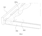
- the LED bar 301 and the light-guide plate 302 of the backlight module of the present embodiment have the same configuration as those in embodiment 1, and in the present embodiment, as shown in Fig. 3 , the shape of the indents 303 of the optical film 303 is part of an oval.
- the indents may also have another regular (such as, whole or part of a circle, a parabolic etc) or irregular shape according to the requirement for reducing hotspot effect.
- the indents are preferable in a regular shape to facilitate machining; in one example, the shape of the indents is smoothly curved face.
- This embodiment discloses a display device comprising the backlight module according to embodiment 1 or 2.
- This display device is, for example, a liquid crystal display device.
- the indents of the optical film are located outside of the displaying area of the display device, and for example shielded by the outer frame of the display device, and thereby do not affect display.
- the indents can reduce hotspots appearing in the displaying area but will not affect display in the displaying area.
- This embodiment discloses a method for eliminating hotspot effect of a backlight module.
- the backlight module is, for example, the backlight module according to embodiment 1 or 2.
- the method comprises the following steps:S1: performing optical simulation of the backlight module to simulate hotspot effect;S3: based on simulation results, cutting an edge of the optical film corresponding to the light incident face of the light-guide plate so as to form indents.
- Embodiment 5
- This embodiment discloses a method for eliminating hotspot effect.
- the method of this embodiment is a modification of embodiment 4, comprising the following steps:
- step S2 comprises:
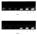
- Figs. 4 and 5 illustrate the resultant presentation achieved from two times of optical simulations for the backlight module.
- the indents of the optical film of the backlight module are of a semi ellipse shape having a semi-major axis of 20mm and a semi-minor axis of 8mm;
- the indents of the optical film of the backlight module is of a semi ellipse shape having a semi-major axis of 20mm and a semi-minor axis of 10mm.
- Table 1 shows the simulation values of brightness of three test points (points 1, 2 and 3) where hotspot effect occurs as well as the test point (point 4) where hotspot effect does not occur in the above two backlight modules before and after cutting.
- Table 1 Simulation values of brightness of four test points (points 1, 2, 3 and 4) before and after cutting Test point Point 1 Point 2 Point 3 Point 4 First backlight module Pre-cutting brightness (nit) 6158 6446 6245 3800 Post-cutting brightness (nit) 4762 4572 4644 3800 Second backlight module Pre-cutting brightness (nit) 6811 6760 6848 3800 Post-cutting brightness (nit) 3952 4065 4055 3800
- step S2 can be omitted in another embodiment of the present invention, such as embodiment 4, that is, the shape of the indents is not optimized.
- favorable indents may be selected artificially as a matter of experience to perform cutting of the optical film.
- the embodiments of the present invention can more quickly and effectively eliminate hotspot effect of a backlight module, achieving better display effect of a display device.
Landscapes
- Physics & Mathematics (AREA)
- Optics & Photonics (AREA)
- General Physics & Mathematics (AREA)
- Engineering & Computer Science (AREA)
- Nonlinear Science (AREA)
- General Engineering & Computer Science (AREA)
- Microelectronics & Electronic Packaging (AREA)
- Mathematical Physics (AREA)
- Chemical & Material Sciences (AREA)
- Crystallography & Structural Chemistry (AREA)
- Planar Illumination Modules (AREA)
- Liquid Crystal (AREA)
- Fastening Of Light Sources Or Lamp Holders (AREA)
Abstract
Description
- Embodiments of the present invention relate to a backlight module, a display device and a method for eliminating hotspot effect.
- A conventional side-illuminating liquid crystal display device comprises a backlight module of the configuration as shown in
Fig.1 . The backlight module comprises a light-guide plate 102, anoptical film 103 provided on a side of thelight emitting face 102b of the light-guide plate 102, andLED bar 101 provided on a side of thelight incident face 102a of the light-guide plate 102. TheLED bar 101 comprisesseveral LEDs 101a disposed at the side thereof facing the light-guide plate 102, the light emitted from theLEDs 101a enters the light-guide plate 102 through thelight incident face 102 of the light-guide plate 102 and then is guided to theoptical film 103. Because theLEDs 101 usually are distributed separately along the length direction of theLED bar 101, hotspots causing uneven shade readily appears at the edge of the light-guide plate 102 adjacent to thelight incident face 102a. When such a backlight module is used in the display device, the hotspots will spread from the non-displaying area to the displaying area of the display device, and then influence the display effect in the displaying area. When hotspot phenomenon occurs, it's generally required to regulate the grid point design of the light-guide plate, return the light-guide plate to its supplier for regulation, and the regulation period is relatively long, and the regulated effect is not good. - Embodiments of the present invention provide a backlight module, a display device and a method for eliminating the hotspot effect, to quickly and effectively eliminate the hotspot effect.
- A first aspect of the present invention provides a side-illuminating backlight module, comprising light-guide plate, an optical film attaching to a side of a light emitting face of the light-guide plate, and a strip-like assembly of point light source disposed at the side of the light incident face of the light-guide plate; the strip-like assembly of point light source comprises point light sources toward the light incident face of the light-guide plate thereon, an edge of one side of the optical film corresponding to the light incident face of the light-guide plate is provided with indents.
- In the backlight module, for example, the point light sources may be LEDs, the strip-like assembly of point light source may be an LED bar.
- In the backlight module, for example, the indents may correspond to the point light sources in position.
- In the backlight module, for example, the shape of the indents may be part of an oval.
- A second aspect of the present invention further provides a display device comprising the above mentioned backlight module.
- In the display device, for example, the indents of the optical film may be located outside of a displaying area of the display device.
- A third aspect of the present invention provides a method for eliminating hotspots of a backlight module, the backlight module comprising a light-guide plate, an optical film attaching to a side of a light emitting face of the light-guide plate, and a strip-like assembly of point light source positioned at the side of the light incident face of the light-guide plate, the strip-like assembly of point light source comprises point light sources toward the light incident face of the light-guide plate thereon, and the method comprises the following steps:
- S1: performing optical simulation of the backlight module to simulate hotspot effect;
- S3: based on simulation results, cutting an edge of the optical film corresponding to the light incident face of the light-guide plate so as to form indents.
- The method, for example, may further comprise, between step S1 and S3, step S2 of optimizing the shape of the indents to be formed for the optical film of the backlight module.
- In this method, for example, the step S2 may comprise:
- S21: based on the simulated extent of hotspot effect, performing simulation cutting for the optical film of the backlight module to achieve simulation indents, then performing optical simulation of the backlight module to simulate hotspot effect; and
- S22: if stimulation extent of hotspot effect does not yet reach predetermined expectation, then regulating a shape and size of the simulation indents of the optical film and returning to step S21; and if obtained extent of hotspot effect reaches the predetermined expectation, then using the obtained simulation indents for the indents to be formed for the optical film and returning to step S3.
- The backlight module provided in an embodiment of the present invention makes the incident light distributed evenly by providing indents for the optical film of the backlight module so as to effectively and quickly eliminate the hotspot effect of the backlight module.
- The display device provided in an embodiment of the present invention, by using the above described backlight module, and makes it not easy for hotspot effect to occur or the extent of hotspot effect relatively gentle in the display device.The method for eliminating hotspot effect provided in an embodiment of the present invention eliminates or reduces the hotspot effect by simulating the backlight module to obtain the extent of hotspot effect and then by cutting the optical film to form indents.
- In order to illustrate the technical solution of the embodiments of the present invention more clearly, a simply introduction about the drawings of the embodiments will be made in the following, and obviously, the drawings described below relate to only some embodiments of the present invention but are not of limitation to the present invention.
-
Fig. 1 is a structural schematic view of a backlight module of conventional side-illuminating liquid crystal display; -
Fig. 2 is a structural schematic view of a backlight module according to a first embodiment of the present invention; -
Fig. 3 is a structural schematic view of a backlight module according to a second embodiment of the present invention; -
Fig. 4 is a resultant schematic view of the optical simulation of the optical film after simulation cutting of optical film according to a fifth embodiment of the present invention; and -
Fig.5 is a resultant schematic view of the optical simulation of the optical film after another simulation cutting of the optical film according to a fourth embodiment of the present invention. - 101: LED bar; 101a: LED; 102: light-guide plate; 102a: light incident face; 102b: light emitting face; 103: optical film; 201: LED bar; 201a: LED; 202: light-guide plate; 202a: light incident face; 202b: light emitting face; 203: optical film; 203a: indent; 301: LED bar; 302: light-guide plate; 303: optical film; 303a: indent.
- To make clearer the object, technical solutions and advantages of the embodiments of the present invention, a clear and full description of the technical solution of the embodiment of the present invention will be made with reference to the accompanying drawings of the embodiment of the present invention. Obviously, the described embodiments are merely part of the embodiments of the present invention, but not all the embodiments. Based on the described embodiments of the present invention, all the other embodiments acquired by the ordinary skilled in this art, without any creative labor, fall into the protective scope of the present invention.
- Unless defined otherwise, the technical or scientific terminology being used should take the meaning usually understood by the ordinary skilled in this art of the present invention. The phrase such as "first", "second" or the like used in the patent application specification and claims of the present invention does not mean any sequence, quantity or importance, but are only used to distinguish different components. Similarly, the phrase such as "a", "an" or "the" does not mean quantitative restriction, but mean the existence of at least one object. The phrase such as "comprise," "include," "contain" or the like intends to mean that the element or article before the phrase encompass the elements or articles and the equallent thereof listed after the phrase, and does not exclude other element(s) or article(s). "Connecting," "connected" or the like is not limited to physical or mechanical connection, but may comprise electrical connection regardless of being direct or indirect. Furthermore, the phrase such as "upper", "lower", "left", "right", or the like is used only for describing a relative positional relationship, which will be varied correspondingly when the described objects are changed in its absolute position.
- As shown in
Fig. 2 , the present embodiment discloses a backlight module, which is a side-illuminating backlight module, comprising a light-guide plate 202, anoptical film 203 attached to a side of thelight emitting face 202b of the light-guide plate 202, and anLED bar 201 located at a side of thelight incident face 202a of the light-guide plate 202.TheLED bar 201 comprisesseveral LEDs 201a facing thelight incident face 202a of the light-guide plate 202 provided on theLED bar 201; and the edge of the side of theoptical film 203 corresponding to thelight incident face 202a of the light-guide plate 202 is provided withseveral indents 203a. - An
LED 201a is an example of the point light source; and theLED bar 201 is an example of a strip-like assembly of point light sources. - An example of the
optical film 203 comprises a light diffusion film, a brightness enhancement film or the like. The light-guide plate is made of, for example, a resin material, and may be a plate in a flat form or a wedge form. In the embodiments, there may be further provided with reflector plate or may be formed with a reflector configuration at a side of the light-guide plate, which side is opposite to thelight emitting face 202b. - For example, the
indents 203a may correspond to theLEDs 201a in their positions, such as, in one-to-one correspondence. The lateral dimension of eachindent 203a (i.e., the dimension along the light incident face of the light-guide plate) is, for example, equivalent to or less than the size of one LED, and the longitudinal dimension thereof (i.e., the height perpendicular to the light incident face of the light-guide plate) is, for example, 1/5∼1/2 of the lateral dimension, as shown inFig. 2 . - The
LED bar 301 and the light-guide plate 302 of the backlight module of the present embodiment have the same configuration as those inembodiment 1, and in the present embodiment, as shown inFig. 3 , the shape of theindents 303 of theoptical film 303 is part of an oval. Naturally, in other embodiments of the present invention, the indents may also have another regular (such as, whole or part of a circle, a parabolic etc) or irregular shape according to the requirement for reducing hotspot effect. Absolutely, the indents are preferable in a regular shape to facilitate machining; in one example, the shape of the indents is smoothly curved face. - This embodiment discloses a display device comprising the backlight module according to
embodiment 1 or 2.This display device is, for example, a liquid crystal display device. - For example, the indents of the optical film are located outside of the displaying area of the display device, and for example shielded by the outer frame of the display device, and thereby do not affect display. The indents can reduce hotspots appearing in the displaying area but will not affect display in the displaying area.
- This embodiment discloses a method for eliminating hotspot effect of a backlight module. The backlight module is, for example, the backlight module according to
embodiment 1 or 2.The method comprises the following steps:S1: performing optical simulation of the backlight module to simulate hotspot effect;S3: based on simulation results, cutting an edge of the optical film corresponding to the light incident face of the light-guide plate so as to form indents.Embodiment 5 - This embodiment discloses a method for eliminating hotspot effect. The method of this embodiment is a modification of
embodiment 4, comprising the following steps: - S1: performing optical simulation of the backlight module to simulate hotspot effect;
- S2: optimizing the shape of the indents to be formed for the optical film of the backlight module;
- S3: based on simulation results, cutting an edge of the optical film corresponding to a light incident face of a light-guide plate so as to form indents.
- In this embodiment, one example of the step S2 comprises:
- S21: based on the resultant extent of the hotspot effect from simulation, performing simulation cutting of the optical film of the backlight module to obtain simulation indents, and then performing optical simulation of the backlight module to simulate hotspot effect;
- S22: if the resultant extent of the simulated hotspot effect from stimulation yet does not reach predetermined expectation, then regulating the shape and size of the simulation indents of the optical film and returning to step S21; and if the resultant extent of the obtained hotspot effect reaches the predetermined expectation, then using the obtained simulation indents for the indents to be formed on the optical film and returning to step S3.
-
Figs. 4 and 5 illustrate the resultant presentation achieved from two times of optical simulations for the backlight module. In the first backlight module corresponding toFig. 4 , the indents of the optical film of the backlight module are of a semi ellipse shape having a semi-major axis of 20mm and a semi-minor axis of 8mm; in the second backlight module corresponding toFig. 5 , the indents of the optical film of the backlight module is of a semi ellipse shape having a semi-major axis of 20mm and a semi-minor axis of 10mm. Table 1 shows the simulation values of brightness of three test points (points 1, 2 and 3) where hotspot effect occurs as well as the test point (point 4) where hotspot effect does not occur in the above two backlight modules before and after cutting.Table 1: Simulation values of brightness of four test points (points 1, 2, 3 and 4) before and after cutting Test point Point 1 Point 2Point 3Point 4First backlight module Pre-cutting brightness (nit) 6158 6446 6245 3800 Post-cutting brightness (nit) 4762 4572 4644 3800 Second backlight module Pre-cutting brightness (nit) 6811 6760 6848 3800 Post-cutting brightness (nit) 3952 4065 4055 3800 - As can be seen from Table 1, before cutting, the brightness of the test points (points 1, 2 and 3) where hotspot effect occurs in the backlight module is relatively higher, while after cutting, the brightness of these test points where hotspot effect occurs is decreased significantly, notably approaching the brightness of the test point (point 4) where hotspot effect does not occur, thereby effectively eliminating the hotspot effect.
- From
Figs. 4 and 5 as well as Table 1, the change of the shapes of the indents also influences the hotspot effect greatly. According to the method of this embodiment, when the optical film of the backlight module are cut to have indents of an appropriate shape, the extent of the hotspot effect may be even more effectively eliminated. - Absolutely, because the extent to which the hotspot effect occurs can be eliminated by forming indents of the optical film only, step S2 can be omitted in another embodiment of the present invention, such as
embodiment 4, that is, the shape of the indents is not optimized. For example, favorable indents may be selected artificially as a matter of experience to perform cutting of the optical film. - From the above embodiments of the present invention, it can be seen that the embodiments of the present invention can more quickly and effectively eliminate hotspot effect of a backlight module, achieving better display effect of a display device.
- The above are only the exemplary embodiments of the present invention, but not limiting the protective scope of the present invention, the protective scope of the present invention is determined by the appended claims.
Claims (9)
- A side-illuminating backlight module, comprising light-guide plate, an optical film attaching to a side of a light emitting face of the light-guide plate, and a strip-like assembly of point light source disposed at the side of the light incident face of the light-guide plate, wherein the strip-like assembly of point light source comprises point light sources toward the light incident face of the light-guide plate thereon, an edge of one side of the optical film corresponding to the light incident face of the light-guide plate is provided with indents.
- The backlight module according to claim 1, wherein the point light sources are LEDs, and the strip-like assembly of point light source is an LED bar.
- The backlight module according to claim 1 or 2, wherein the indents correspond to the point light sources in position.
- The backlight module according to any one of claims 1 to 3, wherein the shape of the indent is part of oval, circle, or parabola.
- A display device comprising the backlight module according to any one of claims 1 to 4.
- The display device according to claim 5, wherein the indents of the optical film are located outside of a displaying area of the display device.
- A method for eliminating hotspots of a backlight module, the backlight module comprising a light-guide plate, an optical film attaching to a side of a light emitting face of the light-guide plate, and a strip-like assembly of point light source positioned at the side of the light incident face of the light-guide plate, the strip-like assembly of point light source comprising point light sources toward the light incident face of the light-guide plate thereon, comprising the following steps:S1: performing optical simulation of the backlight module to simulate hotspot effect;S3: based on simulation results, cutting an edge of the optical film corresponding to the light incident face of the light-guide plate so as to form indents.
- The method for eliminating hotspot effect according to claim 7, furthing comprising, between steps S1 and S3, step S2 of optimizing a shape of the indents to be formed for an optical film of the backlight module.
- The method for eliminating hotspot effect according to claim 8, wherein the step S2 comprises:S21: based on the simulated extent of hotspot effect, performing simulation cutting for the optical film of the backlight module to achieve simulation indents, then performing optical simulation of the backlight module to simulate hotspot effect; andS22: if stimulation extent of hotspot effect does not yet reach predetermined expectation, then regulating a shape and size of the simulation indents of the optical film and returning to step S21; and if obtained extent of hotspot effect reaches the predetermined expectation, then using the obtained simulation indents for the indents to be formed for the optical film and returning to step S3.
Applications Claiming Priority (2)
| Application Number | Priority Date | Filing Date | Title |
|---|---|---|---|
| CN201210271384.1A CN102818187B (en) | 2012-07-31 | 2012-07-31 | Backlight module, display device and method for reducing hot spot phenomenon |
| PCT/CN2012/085190 WO2014019302A1 (en) | 2012-07-31 | 2012-11-23 | Backlight module, display device and method for reducing bright spot phenomenon |
Publications (3)
| Publication Number | Publication Date |
|---|---|
| EP2881656A1 true EP2881656A1 (en) | 2015-06-10 |
| EP2881656A4 EP2881656A4 (en) | 2016-03-16 |
| EP2881656B1 EP2881656B1 (en) | 2021-04-14 |
Family
ID=47302492
Family Applications (1)
| Application Number | Title | Priority Date | Filing Date |
|---|---|---|---|
| EP12852438.6A Active EP2881656B1 (en) | 2012-07-31 | 2012-11-23 | Method for reducing bright spot phenomenon in a backlight module |
Country Status (6)
| Country | Link |
|---|---|
| US (1) | US9207378B2 (en) |
| EP (1) | EP2881656B1 (en) |
| JP (1) | JP2015530697A (en) |
| KR (1) | KR20140026339A (en) |
| CN (1) | CN102818187B (en) |
| WO (1) | WO2014019302A1 (en) |
Families Citing this family (7)
| Publication number | Priority date | Publication date | Assignee | Title |
|---|---|---|---|---|
| CN103323904A (en) * | 2013-06-21 | 2013-09-25 | 北京京东方光电科技有限公司 | Light guide plate, backlight module and display device including same |
| KR20160042237A (en) | 2014-10-07 | 2016-04-19 | 삼성디스플레이 주식회사 | Light guide panel, back light unit and diplay apparatus comprising the same and method for manufacturing light guide panel |
| US10126480B2 (en) | 2015-08-13 | 2018-11-13 | Apple Inc. | Display backlight with light mixing structures |
| CN106443868A (en) * | 2016-11-22 | 2017-02-22 | 苏州茂立光电科技有限公司 | Light guiding plate capable of eliminating hotspots, processing method and backlight module thereof |
| CN107942568A (en) * | 2017-10-12 | 2018-04-20 | 惠科股份有限公司 | Liquid crystal display device and backlight module thereof |
| TWI670532B (en) * | 2018-12-27 | 2019-09-01 | 友達光電股份有限公司 | Back-light module |
| TWI732663B (en) | 2020-08-24 | 2021-07-01 | 群光電能科技股份有限公司 | Backlight assembly and illuminated touch assembly thereof |
Family Cites Families (13)
| Publication number | Priority date | Publication date | Assignee | Title |
|---|---|---|---|---|
| TWI266120B (en) * | 2003-07-18 | 2006-11-11 | Hon Hai Prec Ind Co Ltd | Back light module and liquid crystal display using the same |
| JP4485999B2 (en) * | 2004-07-09 | 2010-06-23 | スタンレー電気株式会社 | Surface light source device |
| TW200739138A (en) * | 2006-03-17 | 2007-10-16 | Mitsubishi Rayon Co | Prism sheet, planar light source device and method for manufacturing the prism sheet |
| KR20070108991A (en) * | 2006-05-09 | 2007-11-15 | 엘지.필립스 엘시디 주식회사 | Backlight Assembly and Liquid Crystal Display Using Same |
| JP4853784B2 (en) * | 2007-01-12 | 2012-01-11 | ミネベア株式会社 | Surface lighting device |
| US20090251921A1 (en) * | 2008-04-03 | 2009-10-08 | Tpo Displays Corp. | System for improvement of the perceived FOS homogeneity by suppressing hotspots in a module design with a short LED to active area distance |
| JP5429633B2 (en) * | 2009-03-09 | 2014-02-26 | Nltテクノロジー株式会社 | Surface light emitting device and liquid crystal display device |
| TW201118466A (en) * | 2009-11-18 | 2011-06-01 | Coretronic Corp | Backlight module |
| KR101730181B1 (en) | 2009-12-11 | 2017-04-26 | 엘지디스플레이 주식회사 | Backlight unit and liquid crystal display device having the same |
| KR101826719B1 (en) * | 2010-10-13 | 2018-02-08 | 엘지디스플레이 주식회사 | light guide plate and liquid crystal display device module including the same |
| TWI434083B (en) * | 2010-12-01 | 2014-04-11 | Entire Technology Co Ltd | Light guide device and backlight module |
| CN202419364U (en) * | 2011-12-31 | 2012-09-05 | 精元电脑(江苏)有限公司 | Backlight module and light emitting keyboard using same |
| CN102565921A (en) * | 2012-02-16 | 2012-07-11 | 深圳市华星光电技术有限公司 | Light guide plate, backlight module and liquid crystal display device |
-
2012
- 2012-07-31 CN CN201210271384.1A patent/CN102818187B/en active Active
- 2012-11-23 WO PCT/CN2012/085190 patent/WO2014019302A1/en not_active Ceased
- 2012-11-23 US US13/995,948 patent/US9207378B2/en active Active
- 2012-11-23 EP EP12852438.6A patent/EP2881656B1/en active Active
- 2012-11-23 JP JP2015524595A patent/JP2015530697A/en active Pending
- 2012-11-23 KR KR1020137014207A patent/KR20140026339A/en not_active Ceased
Also Published As
| Publication number | Publication date |
|---|---|
| US20140085930A1 (en) | 2014-03-27 |
| EP2881656B1 (en) | 2021-04-14 |
| EP2881656A4 (en) | 2016-03-16 |
| KR20140026339A (en) | 2014-03-05 |
| JP2015530697A (en) | 2015-10-15 |
| CN102818187B (en) | 2015-02-25 |
| CN102818187A (en) | 2012-12-12 |
| US9207378B2 (en) | 2015-12-08 |
| WO2014019302A1 (en) | 2014-02-06 |
Similar Documents
| Publication | Publication Date | Title |
|---|---|---|
| EP2881656A1 (en) | Backlight module, display device and method for reducing bright spot phenomenon | |
| US11733564B2 (en) | Curved backlight module and display device | |
| CN102901002B (en) | Lighting device, display device and electronic equipment | |
| CN103090278B (en) | Backlight module, the television set with this backlight module and display unit | |
| US8408777B2 (en) | Planar illumination device | |
| EP2728248B1 (en) | Light-emitting unit, backlight module and display device | |
| CN102620193A (en) | Sectional light emitting diode (LED) backlight module and liquid crystal display device | |
| EP3200019A1 (en) | Backlight module and display device | |
| CN205191348U (en) | Can realize seamless concatenation panel light of evenly showing up | |
| CN203286495U (en) | Multi-face-light-emitting LED light source, LED lamp strip and backlight module | |
| US20120249921A1 (en) | Light guide plate, liquid crystal display module and liquid crystal display | |
| CN103822139A (en) | Backlight source module and display device | |
| DE202010006989U1 (en) | lighting element | |
| CN104459871A (en) | Light guide plate, backlight module and display device | |
| CN106773286B (en) | Backlight unit for local light control and display device | |
| CN107179632A (en) | Backlight module, display module and display device | |
| CN208270886U (en) | A kind of side entering type narrow frame backlight module that achievable dynamic HDR is shown | |
| CN210345144U (en) | Side light guide frame-free panel lamp | |
| CN207148488U (en) | Backlight module, display device and support member | |
| US20150009447A1 (en) | Backlight module and liquid crystal display | |
| CN110375234B (en) | Processing method of integrated mask for spliced borderless panel lamp | |
| CN106764686A (en) | Backlight module and display device | |
| CN102620210A (en) | LCD (Liquid Crystal Display) device and backlight module thereof | |
| CN203731204U (en) | Direct-lit type liquid crystal display device and backlight module thereof | |
| US9116388B2 (en) | Backlight module and liquid crystal display |
Legal Events
| Date | Code | Title | Description |
|---|---|---|---|
| PUAI | Public reference made under article 153(3) epc to a published international application that has entered the european phase |
Free format text: ORIGINAL CODE: 0009012 |
|
| 17P | Request for examination filed |
Effective date: 20130531 |
|
| AK | Designated contracting states |
Kind code of ref document: A1 Designated state(s): AL AT BE BG CH CY CZ DE DK EE ES FI FR GB GR HR HU IE IS IT LI LT LU LV MC MK MT NL NO PL PT RO RS SE SI SK SM TR |
|
| AX | Request for extension of the european patent |
Extension state: BA ME |
|
| DAX | Request for extension of the european patent (deleted) | ||
| RA4 | Supplementary search report drawn up and despatched (corrected) |
Effective date: 20160212 |
|
| STAA | Information on the status of an ep patent application or granted ep patent |
Free format text: STATUS: EXAMINATION IS IN PROGRESS |
|
| 17Q | First examination report despatched |
Effective date: 20170811 |
|
| RIC1 | Information provided on ipc code assigned before grant |
Ipc: G02F 1/13357 20060101ALI20200918BHEP Ipc: F21V 8/00 20060101AFI20200918BHEP |
|
| GRAP | Despatch of communication of intention to grant a patent |
Free format text: ORIGINAL CODE: EPIDOSNIGR1 |
|
| STAA | Information on the status of an ep patent application or granted ep patent |
Free format text: STATUS: GRANT OF PATENT IS INTENDED |
|
| INTG | Intention to grant announced |
Effective date: 20201111 |
|
| GRAS | Grant fee paid |
Free format text: ORIGINAL CODE: EPIDOSNIGR3 |
|
| GRAA | (expected) grant |
Free format text: ORIGINAL CODE: 0009210 |
|
| STAA | Information on the status of an ep patent application or granted ep patent |
Free format text: STATUS: THE PATENT HAS BEEN GRANTED |
|
| AK | Designated contracting states |
Kind code of ref document: B1 Designated state(s): AL AT BE BG CH CY CZ DE DK EE ES FI FR GB GR HR HU IE IS IT LI LT LU LV MC MK MT NL NO PL PT RO RS SE SI SK SM TR |
|
| REG | Reference to a national code |
Ref country code: GB Ref legal event code: FG4D |
|
| REG | Reference to a national code |
Ref country code: CH Ref legal event code: EP |
|
| REG | Reference to a national code |
Ref country code: DE Ref legal event code: R096 Ref document number: 602012075251 Country of ref document: DE |
|
| REG | Reference to a national code |
Ref country code: IE Ref legal event code: FG4D |
|
| REG | Reference to a national code |
Ref country code: AT Ref legal event code: REF Ref document number: 1382724 Country of ref document: AT Kind code of ref document: T Effective date: 20210515 |
|
| REG | Reference to a national code |
Ref country code: LT Ref legal event code: MG9D |
|
| REG | Reference to a national code |
Ref country code: AT Ref legal event code: MK05 Ref document number: 1382724 Country of ref document: AT Kind code of ref document: T Effective date: 20210414 |
|
| REG | Reference to a national code |
Ref country code: NL Ref legal event code: MP Effective date: 20210414 |
|
| PG25 | Lapsed in a contracting state [announced via postgrant information from national office to epo] |
Ref country code: LT Free format text: LAPSE BECAUSE OF FAILURE TO SUBMIT A TRANSLATION OF THE DESCRIPTION OR TO PAY THE FEE WITHIN THE PRESCRIBED TIME-LIMIT Effective date: 20210414 Ref country code: NL Free format text: LAPSE BECAUSE OF FAILURE TO SUBMIT A TRANSLATION OF THE DESCRIPTION OR TO PAY THE FEE WITHIN THE PRESCRIBED TIME-LIMIT Effective date: 20210414 Ref country code: FI Free format text: LAPSE BECAUSE OF FAILURE TO SUBMIT A TRANSLATION OF THE DESCRIPTION OR TO PAY THE FEE WITHIN THE PRESCRIBED TIME-LIMIT Effective date: 20210414 Ref country code: HR Free format text: LAPSE BECAUSE OF FAILURE TO SUBMIT A TRANSLATION OF THE DESCRIPTION OR TO PAY THE FEE WITHIN THE PRESCRIBED TIME-LIMIT Effective date: 20210414 Ref country code: AT Free format text: LAPSE BECAUSE OF FAILURE TO SUBMIT A TRANSLATION OF THE DESCRIPTION OR TO PAY THE FEE WITHIN THE PRESCRIBED TIME-LIMIT Effective date: 20210414 Ref country code: BG Free format text: LAPSE BECAUSE OF FAILURE TO SUBMIT A TRANSLATION OF THE DESCRIPTION OR TO PAY THE FEE WITHIN THE PRESCRIBED TIME-LIMIT Effective date: 20210714 |
|
| PG25 | Lapsed in a contracting state [announced via postgrant information from national office to epo] |
Ref country code: NO Free format text: LAPSE BECAUSE OF FAILURE TO SUBMIT A TRANSLATION OF THE DESCRIPTION OR TO PAY THE FEE WITHIN THE PRESCRIBED TIME-LIMIT Effective date: 20210714 Ref country code: PT Free format text: LAPSE BECAUSE OF FAILURE TO SUBMIT A TRANSLATION OF THE DESCRIPTION OR TO PAY THE FEE WITHIN THE PRESCRIBED TIME-LIMIT Effective date: 20210816 Ref country code: PL Free format text: LAPSE BECAUSE OF FAILURE TO SUBMIT A TRANSLATION OF THE DESCRIPTION OR TO PAY THE FEE WITHIN THE PRESCRIBED TIME-LIMIT Effective date: 20210414 Ref country code: ES Free format text: LAPSE BECAUSE OF FAILURE TO SUBMIT A TRANSLATION OF THE DESCRIPTION OR TO PAY THE FEE WITHIN THE PRESCRIBED TIME-LIMIT Effective date: 20210414 Ref country code: IS Free format text: LAPSE BECAUSE OF FAILURE TO SUBMIT A TRANSLATION OF THE DESCRIPTION OR TO PAY THE FEE WITHIN THE PRESCRIBED TIME-LIMIT Effective date: 20210814 Ref country code: LV Free format text: LAPSE BECAUSE OF FAILURE TO SUBMIT A TRANSLATION OF THE DESCRIPTION OR TO PAY THE FEE WITHIN THE PRESCRIBED TIME-LIMIT Effective date: 20210414 Ref country code: GR Free format text: LAPSE BECAUSE OF FAILURE TO SUBMIT A TRANSLATION OF THE DESCRIPTION OR TO PAY THE FEE WITHIN THE PRESCRIBED TIME-LIMIT Effective date: 20210715 Ref country code: RS Free format text: LAPSE BECAUSE OF FAILURE TO SUBMIT A TRANSLATION OF THE DESCRIPTION OR TO PAY THE FEE WITHIN THE PRESCRIBED TIME-LIMIT Effective date: 20210414 Ref country code: SE Free format text: LAPSE BECAUSE OF FAILURE TO SUBMIT A TRANSLATION OF THE DESCRIPTION OR TO PAY THE FEE WITHIN THE PRESCRIBED TIME-LIMIT Effective date: 20210414 |
|
| REG | Reference to a national code |
Ref country code: DE Ref legal event code: R097 Ref document number: 602012075251 Country of ref document: DE |
|
| PG25 | Lapsed in a contracting state [announced via postgrant information from national office to epo] |
Ref country code: CZ Free format text: LAPSE BECAUSE OF FAILURE TO SUBMIT A TRANSLATION OF THE DESCRIPTION OR TO PAY THE FEE WITHIN THE PRESCRIBED TIME-LIMIT Effective date: 20210414 Ref country code: EE Free format text: LAPSE BECAUSE OF FAILURE TO SUBMIT A TRANSLATION OF THE DESCRIPTION OR TO PAY THE FEE WITHIN THE PRESCRIBED TIME-LIMIT Effective date: 20210414 Ref country code: DK Free format text: LAPSE BECAUSE OF FAILURE TO SUBMIT A TRANSLATION OF THE DESCRIPTION OR TO PAY THE FEE WITHIN THE PRESCRIBED TIME-LIMIT Effective date: 20210414 Ref country code: SM Free format text: LAPSE BECAUSE OF FAILURE TO SUBMIT A TRANSLATION OF THE DESCRIPTION OR TO PAY THE FEE WITHIN THE PRESCRIBED TIME-LIMIT Effective date: 20210414 Ref country code: SK Free format text: LAPSE BECAUSE OF FAILURE TO SUBMIT A TRANSLATION OF THE DESCRIPTION OR TO PAY THE FEE WITHIN THE PRESCRIBED TIME-LIMIT Effective date: 20210414 Ref country code: RO Free format text: LAPSE BECAUSE OF FAILURE TO SUBMIT A TRANSLATION OF THE DESCRIPTION OR TO PAY THE FEE WITHIN THE PRESCRIBED TIME-LIMIT Effective date: 20210414 |
|
| PLBE | No opposition filed within time limit |
Free format text: ORIGINAL CODE: 0009261 |
|
| STAA | Information on the status of an ep patent application or granted ep patent |
Free format text: STATUS: NO OPPOSITION FILED WITHIN TIME LIMIT |
|
| 26N | No opposition filed |
Effective date: 20220117 |
|
| PG25 | Lapsed in a contracting state [announced via postgrant information from national office to epo] |
Ref country code: IS Free format text: LAPSE BECAUSE OF FAILURE TO SUBMIT A TRANSLATION OF THE DESCRIPTION OR TO PAY THE FEE WITHIN THE PRESCRIBED TIME-LIMIT Effective date: 20210814 Ref country code: AL Free format text: LAPSE BECAUSE OF FAILURE TO SUBMIT A TRANSLATION OF THE DESCRIPTION OR TO PAY THE FEE WITHIN THE PRESCRIBED TIME-LIMIT Effective date: 20210414 |
|
| PG25 | Lapsed in a contracting state [announced via postgrant information from national office to epo] |
Ref country code: MC Free format text: LAPSE BECAUSE OF FAILURE TO SUBMIT A TRANSLATION OF THE DESCRIPTION OR TO PAY THE FEE WITHIN THE PRESCRIBED TIME-LIMIT Effective date: 20210414 |
|
| REG | Reference to a national code |
Ref country code: CH Ref legal event code: PL |
|
| GBPC | Gb: european patent ceased through non-payment of renewal fee |
Effective date: 20211123 |
|
| PG25 | Lapsed in a contracting state [announced via postgrant information from national office to epo] |
Ref country code: LU Free format text: LAPSE BECAUSE OF NON-PAYMENT OF DUE FEES Effective date: 20211123 Ref country code: IT Free format text: LAPSE BECAUSE OF FAILURE TO SUBMIT A TRANSLATION OF THE DESCRIPTION OR TO PAY THE FEE WITHIN THE PRESCRIBED TIME-LIMIT Effective date: 20210414 Ref country code: BE Free format text: LAPSE BECAUSE OF NON-PAYMENT OF DUE FEES Effective date: 20211130 |
|
| REG | Reference to a national code |
Ref country code: BE Ref legal event code: MM Effective date: 20211130 |
|
| PG25 | Lapsed in a contracting state [announced via postgrant information from national office to epo] |
Ref country code: LI Free format text: LAPSE BECAUSE OF NON-PAYMENT OF DUE FEES Effective date: 20211130 Ref country code: CH Free format text: LAPSE BECAUSE OF NON-PAYMENT OF DUE FEES Effective date: 20211130 |
|
| PG25 | Lapsed in a contracting state [announced via postgrant information from national office to epo] |
Ref country code: IE Free format text: LAPSE BECAUSE OF NON-PAYMENT OF DUE FEES Effective date: 20211123 Ref country code: GB Free format text: LAPSE BECAUSE OF NON-PAYMENT OF DUE FEES Effective date: 20211123 |
|
| PG25 | Lapsed in a contracting state [announced via postgrant information from national office to epo] |
Ref country code: FR Free format text: LAPSE BECAUSE OF NON-PAYMENT OF DUE FEES Effective date: 20211130 |
|
| PG25 | Lapsed in a contracting state [announced via postgrant information from national office to epo] |
Ref country code: HU Free format text: LAPSE BECAUSE OF FAILURE TO SUBMIT A TRANSLATION OF THE DESCRIPTION OR TO PAY THE FEE WITHIN THE PRESCRIBED TIME-LIMIT; INVALID AB INITIO Effective date: 20121123 Ref country code: CY Free format text: LAPSE BECAUSE OF FAILURE TO SUBMIT A TRANSLATION OF THE DESCRIPTION OR TO PAY THE FEE WITHIN THE PRESCRIBED TIME-LIMIT Effective date: 20210414 |
|
| PG25 | Lapsed in a contracting state [announced via postgrant information from national office to epo] |
Ref country code: MK Free format text: LAPSE BECAUSE OF FAILURE TO SUBMIT A TRANSLATION OF THE DESCRIPTION OR TO PAY THE FEE WITHIN THE PRESCRIBED TIME-LIMIT Effective date: 20210414 |
|
| PG25 | Lapsed in a contracting state [announced via postgrant information from national office to epo] |
Ref country code: MT Free format text: LAPSE BECAUSE OF FAILURE TO SUBMIT A TRANSLATION OF THE DESCRIPTION OR TO PAY THE FEE WITHIN THE PRESCRIBED TIME-LIMIT Effective date: 20210414 |
|
| PG25 | Lapsed in a contracting state [announced via postgrant information from national office to epo] |
Ref country code: TR Free format text: LAPSE BECAUSE OF FAILURE TO SUBMIT A TRANSLATION OF THE DESCRIPTION OR TO PAY THE FEE WITHIN THE PRESCRIBED TIME-LIMIT Effective date: 20210414 |
|
| PGFP | Annual fee paid to national office [announced via postgrant information from national office to epo] |
Ref country code: DE Payment date: 20251121 Year of fee payment: 14 |