EP2879197A1 - Organic light emitting display apparatus and method for manufacturing the same - Google Patents
Organic light emitting display apparatus and method for manufacturing the same Download PDFInfo
- Publication number
- EP2879197A1 EP2879197A1 EP14194161.7A EP14194161A EP2879197A1 EP 2879197 A1 EP2879197 A1 EP 2879197A1 EP 14194161 A EP14194161 A EP 14194161A EP 2879197 A1 EP2879197 A1 EP 2879197A1
- Authority
- EP
- European Patent Office
- Prior art keywords
- layer
- light emitting
- organic light
- organic
- viscoelastic
- Prior art date
- Legal status (The legal status is an assumption and is not a legal conclusion. Google has not performed a legal analysis and makes no representation as to the accuracy of the status listed.)
- Granted
Links
Images





Classifications
-
- H—ELECTRICITY
- H10—SEMICONDUCTOR DEVICES; ELECTRIC SOLID-STATE DEVICES NOT OTHERWISE PROVIDED FOR
- H10K—ORGANIC ELECTRIC SOLID-STATE DEVICES
- H10K59/00—Integrated devices, or assemblies of multiple devices, comprising at least one organic light-emitting element covered by group H10K50/00
- H10K59/80—Constructional details
- H10K59/87—Passivation; Containers; Encapsulations
- H10K59/871—Self-supporting sealing arrangements
- H10K59/8722—Peripheral sealing arrangements, e.g. adhesives, sealants
-
- H—ELECTRICITY
- H10—SEMICONDUCTOR DEVICES; ELECTRIC SOLID-STATE DEVICES NOT OTHERWISE PROVIDED FOR
- H10K—ORGANIC ELECTRIC SOLID-STATE DEVICES
- H10K59/00—Integrated devices, or assemblies of multiple devices, comprising at least one organic light-emitting element covered by group H10K50/00
- H10K59/80—Constructional details
- H10K59/87—Passivation; Containers; Encapsulations
- H10K59/873—Encapsulations
-
- H—ELECTRICITY
- H10—SEMICONDUCTOR DEVICES; ELECTRIC SOLID-STATE DEVICES NOT OTHERWISE PROVIDED FOR
- H10K—ORGANIC ELECTRIC SOLID-STATE DEVICES
- H10K50/00—Organic light-emitting devices
- H10K50/80—Constructional details
- H10K50/84—Passivation; Containers; Encapsulations
- H10K50/844—Encapsulations
-
- H—ELECTRICITY
- H10—SEMICONDUCTOR DEVICES; ELECTRIC SOLID-STATE DEVICES NOT OTHERWISE PROVIDED FOR
- H10K—ORGANIC ELECTRIC SOLID-STATE DEVICES
- H10K59/00—Integrated devices, or assemblies of multiple devices, comprising at least one organic light-emitting element covered by group H10K50/00
- H10K59/40—OLEDs integrated with touch screens
-
- H—ELECTRICITY
- H10—SEMICONDUCTOR DEVICES; ELECTRIC SOLID-STATE DEVICES NOT OTHERWISE PROVIDED FOR
- H10K—ORGANIC ELECTRIC SOLID-STATE DEVICES
- H10K59/00—Integrated devices, or assemblies of multiple devices, comprising at least one organic light-emitting element covered by group H10K50/00
- H10K59/80—Constructional details
- H10K59/87—Passivation; Containers; Encapsulations
-
- H—ELECTRICITY
- H10—SEMICONDUCTOR DEVICES; ELECTRIC SOLID-STATE DEVICES NOT OTHERWISE PROVIDED FOR
- H10K—ORGANIC ELECTRIC SOLID-STATE DEVICES
- H10K59/00—Integrated devices, or assemblies of multiple devices, comprising at least one organic light-emitting element covered by group H10K50/00
- H10K59/80—Constructional details
- H10K59/8791—Arrangements for improving contrast, e.g. preventing reflection of ambient light
-
- H—ELECTRICITY
- H10—SEMICONDUCTOR DEVICES; ELECTRIC SOLID-STATE DEVICES NOT OTHERWISE PROVIDED FOR
- H10K—ORGANIC ELECTRIC SOLID-STATE DEVICES
- H10K2102/00—Constructional details relating to the organic devices covered by this subclass
- H10K2102/301—Details of OLEDs
- H10K2102/311—Flexible OLED
-
- H—ELECTRICITY
- H10—SEMICONDUCTOR DEVICES; ELECTRIC SOLID-STATE DEVICES NOT OTHERWISE PROVIDED FOR
- H10K—ORGANIC ELECTRIC SOLID-STATE DEVICES
- H10K50/00—Organic light-emitting devices
- H10K50/80—Constructional details
- H10K50/84—Passivation; Containers; Encapsulations
- H10K50/844—Encapsulations
- H10K50/8445—Encapsulations multilayered coatings having a repetitive structure, e.g. having multiple organic-inorganic bilayers
-
- H—ELECTRICITY
- H10—SEMICONDUCTOR DEVICES; ELECTRIC SOLID-STATE DEVICES NOT OTHERWISE PROVIDED FOR
- H10K—ORGANIC ELECTRIC SOLID-STATE DEVICES
- H10K50/00—Organic light-emitting devices
- H10K50/80—Constructional details
- H10K50/85—Arrangements for extracting light from the devices
-
- H—ELECTRICITY
- H10—SEMICONDUCTOR DEVICES; ELECTRIC SOLID-STATE DEVICES NOT OTHERWISE PROVIDED FOR
- H10K—ORGANIC ELECTRIC SOLID-STATE DEVICES
- H10K50/00—Organic light-emitting devices
- H10K50/80—Constructional details
- H10K50/86—Arrangements for improving contrast, e.g. preventing reflection of ambient light
-
- H—ELECTRICITY
- H10—SEMICONDUCTOR DEVICES; ELECTRIC SOLID-STATE DEVICES NOT OTHERWISE PROVIDED FOR
- H10K—ORGANIC ELECTRIC SOLID-STATE DEVICES
- H10K59/00—Integrated devices, or assemblies of multiple devices, comprising at least one organic light-emitting element covered by group H10K50/00
- H10K59/80—Constructional details
- H10K59/87—Passivation; Containers; Encapsulations
- H10K59/873—Encapsulations
- H10K59/8731—Encapsulations multilayered coatings having a repetitive structure, e.g. having multiple organic-inorganic bilayers
-
- H—ELECTRICITY
- H10—SEMICONDUCTOR DEVICES; ELECTRIC SOLID-STATE DEVICES NOT OTHERWISE PROVIDED FOR
- H10K—ORGANIC ELECTRIC SOLID-STATE DEVICES
- H10K59/00—Integrated devices, or assemblies of multiple devices, comprising at least one organic light-emitting element covered by group H10K50/00
- H10K59/80—Constructional details
- H10K59/875—Arrangements for extracting light from the devices
Definitions
- the present disclosure relates to an organic light emitting display apparatus and method for manufacturing the same, and more particularly, to an organic light emitting display apparatus and method for manufacturing the same that is capable of reducing visually recognizable bubbles in the encapsulation structure.
- LCD liquid crystal display
- an organic light emitting display (OLED) apparatus As a flat panel display apparatus that may solve such drawbacks of the LCD apparatus, an organic light emitting display (OLED) apparatus has received attention. Since the OLED apparatus is an emissive apparatus that generates light by itself, the OLED apparatus has brightness, contrast ratio and viewing angle that are better than those of the non-emissive apparatus. Also, since the OLED apparatus does not require a separate backlight, the OLED apparatus may be more lightweight and thinner than the LCD apparatus, and may consume less power than the LCD apparatus.
- the OLED apparatus typically includes a thin film transistor, a first electrode electrically connected with the thin film transistor, a light-emissive organic layer on the first electrode, and a second electrode on the light-emissive organic layer.
- an encapsulation structure is typically provided to prevent a light-emissive defect caused by permeation of water and oxygen into the light-emissive organic layer.
- FIGs. 1 and 2 briefly illustrate cross-sectional views of OLED apparatuses having different encapsulation structures (hereinafter, referred to as "first and second type encapsulation structures").
- these OLED apparatuses are substantially identical to each other in that they include a TFT substrate 10, which includes a thin film transistor (not shown), and an organic light emitting element 20 on the TFT substrate 10.
- the organic light emitting element 20 includes a first electrode 21 on the TFT substrate 10, which is electrically connected with the thin film transistor, a bank layer 22 formed on the TFT substrate 10 on which the first electrode 21 is formed and having a bank hole for exposing at least a part of the first electrode 21 corresponding to a light emitting area, a light-emissive organic layer 23 on the part of the first electrode 21, which is exposed through the bank hole of the bank layer 22, and a second electrode 24 on the light-emissive organic layer 23.
- the first type encapsulation structure includes an encapsulation glass 31 spaced apart from the organic light emitting element 20 at a predetermined distance, and a frit layer 32 disposed between the TFT substrate 10 and the encapsulation glass 31 at corners of the OLED apparatus.
- the encapsulation glass 31 mainly prevents oxygen/water from being permeated into the light-emissive organic layer 23 through a face of the OLED apparatus, and the frit layer 32 mainly prevents oxygen/water from being permeated into the light-emissive organic layer 23 through a side of the organic light emitting display apparatus.
- the OLED apparatus having the first type encapsulation structure has a problem in that the OLED apparatus is vulnerable to external impact, and thus may not be suitable for a flexible display apparatus.
- the second type encapsulation structure has been suggested.
- a passivation layer 40 is formed on the TFT substrate 10, in which the organic light emitting element 20 is formed, to fully cover the organic light emitting device 20. Subsequently, an encapsulation film 60 is bonded onto the TFT substrate 10, on which the passivation layer 40 is formed, using an adhesive layer 50.
- the encapsulation film 60, the adhesive layer 50 and the passivation layer 40 mainly prevent oxygen/water from being permeated into the light-emissive organic layer 23 through the face of the organic light emitting display apparatus, and the adhesive layer 50 and the passivation layer 40 mainly prevent oxygen/water from being permeated into the light-emissive organic layer 23 through the side of the organic light emitting display apparatus.
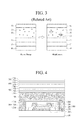
- the conventional adhesive layer 50 applied to the second type encapsulation structure has relatively low heat-resistance. Due to such low heat-resistance and difference in coefficient of thermal expansion with an adjacent structure, the adhesive layer 50 may be thermally deformed under an environment of high temperature and high humidity, as illustrated in FIG. 3 . This may lead to a problem in that fine bubbles 51 inside the adhesive layer 50 are combined with one another to generate bubble(s) 52 that may be recognized visually.
- These bubbles may be regarded as a product defect, and thus the productivity of the OLED apparatus may be lowered.
- the occurrence of these bubbles after the product has been sold may lower reliability and damage the brand image.
- the present invention is directed to an organic light emitting display apparatus and method for manufacturing the same, which substantially obviates one or more problems due to limitations and disadvantages of the related art.
- An advantage of the present invention is to provide an organic light emitting display apparatus and method for manufacturing the same that is capable of reducing visually recognizable bubbles that otherwise might be generated under an environment of high temperature and high humidity within the encapsulation structure.
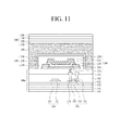
- FIG. 4 briefly illustrates a cross-section of an organic light emitting display (OLED) apparatus according to an embodiment of the present invention.
- the OLED apparatus includes a TFT substrate 100, which includes a thin film transistor, an organic light emitting element 200, a passivation layer 300 formed on the organic light emitting element 200 to cover the organic light emitting element 200, a viscoelastic layer 400 formed on the passivation layer 300 to cover the passivation layer 300, and an encapsulation film 500 on the viscoelastic layer 400.
- the OLED apparatus may further include a circular polarizing plate 600 on the encapsulation film 500, and a front module 700 on the circular polarizing plate 600.
- FIG. 5 briefly illustrates a cross-section of a TFT substrate 100 according to an embodiment of the present invention.
- the TFT substrate 100 includes a polyimide film 110, a buffer layer 120 on one surface of the polyimide film 110, a thin film transistor 130 and a capacitor 140 formed on the buffer layer 120, and a rear plate 190 attached onto another surface of the polyimide film 110 using an adhesive layer 180.
- the thin film transistor 130 includes a semiconductor layer 131, a gate electrode 132, and source and drain electrodes 133 and 134.
- the capacitor 140 includes a capacitor lower electrode 141 and a capacitor upper electrode 142.
- a gate insulating film 150 is formed between the semiconductor layer 131 and the gate electrode 132 and between the capacitor lower electrode 141 and the capacitor upper electrode 142.
- An interlayer insulating film 160 is formed on the capacitor upper electrode 142 and between the gate electrode 132 and the source and drain electrodes 133 and 134.
- An overcoat layer 170 is formed on the interlayer insulating film 160 and the source and drain electrodes 133 and 134 in order to passivate the thin film transistor 130 and the capacitor 140 and planarize a step difference caused by the thin film transistor 130.
- a first electrode 210 of the organic light emitting element 200 is electrically connected with the drain electrode 134 of the thin film transistor 130 through a hole formed in the overcoat layer 170.
- the TFT substrate 100 illustrated in FIG. 5 has a structure for a flexible display apparatus and includes a top-gate type thin film transistor where the gate electrode 132 is disposed above the semiconductor layer 131, the present invention is not limited to such a structure of FIG. 5 , and the TFT substrate 100 may include a bottom-gate type thin film transistor where the gate electrode is located below the semiconductor layer or have a non-flexible structure.
- the TFT substrate 100' includes a substrate 111 formed of glass or plastic material, a gate electrode 113a on the substrate 111, a gate insulating film 112 and the gate electrode 113a, a semiconductor layer 113b overlapped with the gate electrode 113a, with the gate insulating film 112 interposed between the semiconductor 113b and the gate electrode 113a, source and drain electrodes 113c and 113d spaced apart from each other on the gate insulating film 112 and the semiconductor layer 113b, and an inorganic insulating film 114 and an organic insulating film 115 sequentially formed on the substrate 111 provided with the thin film transistor 113.
- the first electrode 210 of the organic light emitting element 200 is electrically connected with the drain electrode 113d of the thin film transistor 113 through a hole formed in the inorganic insulating film 114 and the organic insulating film 115.
- the organic light emitting element 200 includes a first electrode 210 on the TFT substrate 100, a bank layer 220 formed on the first electrode 210 and having a bank hole to expose at least a part of the first electrode 210 corresponding to a light emitting area, a light-emissive organic layer 230 on the part of the first electrode 210, which is exposed through the bank hole of the bank layer 220, a second electrode 240 on the light-emissive organic layer 230, and a capping layer 250 on the second electrode 240.
- the first electrode 210 is electrically connected with the thin film transistor of the TFT substrate 100 (more specifically, electrically connected with the drain electrode 134).
- the first electrode 210 may be an anode electrode and formed of a transparent conductive material having a high work function, such as indium tin oxide (ITO), indium zinc oxide (IZO), indium tin zinc oxide (ITZO), indium cerium oxide (ICO), or ZnO.
- the bank hole of the bank layer 220 may define the light emitting area by exposing at least a part of the first electrode 210.
- the light-emissive organic layer 230 formed on the first electrode 210 and a part of the bank layer 220 may include a light emitting layer, a hole injection layer and/or a hole transport layer between the first electrode 210 and the light emitting layer, and an electron injection layer and/or an electron transport layer between the second electrode 240 and the light emitting layer.
- the second electrode 240 disposed on the light-emissive organic layer 230 may be a cathode electrode and formed of metal having a low work function such as Al, Mg, Ca, Ag or their alloy.
- the OLED apparatus may be a rear light-emissive type where light emitted from the light-emissive organic layer 230 passes through the TFT substrate 100 or a front light-emissive type where light emitted from the light-emissive organic layer 230 passes through the front module 700.
- the second electrode 240 may have a thickness enough to reflect light.
- the second electrode 240 may have a thickness thin enough (e.g., 1 ⁇ to 50 ⁇ ) to transmit light, and a reflecting layer (not shown) formed of Al, Ag or Ni may be arranged below the first electrode 210.
- the capping layer 250 may be formed on the second electrode 240. The capping layer 250 is used to reduce or prevent the light emitted from the light-emissive organic layer 230 from being totally reflected above the second electrode 240, and may be formed of a mixture of a conductive inorganic material and an organic material.
- a metal for example, transition metal, alkali metal, alkali earth metal, rare-earth metal, or their alloy of two or more metals may be used as the conductive inorganic material.
- An organic material for example, material that may be used as a host material of the hole transport layer) having excellent hole mobility or an organic material (for example, material that may be used as a host material of the electron transport layer) having excellent electron mobility may be used as the organic material.
- the conductive inorganic material may increase scattering of light and absorption of light by generating surface Plasmon resonance at the capping layer 250, and may prevent total reflection from occurring above the second electrode 240, whereby light extraction effect of the OLED apparatus is improved.
- the OLED apparatus includes a passivation layer 300 formed on the TFT substrate 100 to cover the organic light emitting element 200.
- the passivation layer 300 includes a first inorganic layer 310 formed on the TFT substrate 100 and the organic light emitting element 200, an organic layer 320 on the first inorganic layer 310, and a second inorganic layer 330 on the organic layer 320.
- the first and second inorganic layers 310 and 330 may be formed of a material that includes one or more of Al 2 O 3 ;, SiO 2 , Si 3 N 4 , SiON, AlON, AlN, TiO 2 , ZrO, ZnO, and Ta 2 O 5 , and the organic layer 320 may be formed of an organic matter suitable for shielding water/oxygen, such as acryl resin, epoxy resin, polyimide resin, and polyethylene.
- the organic layer 320 serves to reduce stress between the respective layers, which occurs when the OLED apparatus is bent.
- the OLED apparatus further includes a viscoelastic layer 400 formed on the TFT substrate 100 to fully cover the passivation layer 300, and an encapsulation film 500 on the viscoelastic layer 400.
- FIG. 7 is a Maxwell model of a viscoelastic material
- FIG. 8 is a graph illustrating variation of stress with time of a viscoelastic material measured through a relaxation modulus test.
- the viscoelastic layer 400 is formed of a viscoelastic material that may be displayed as a Maxwell model illustrated in FIG. 7 . As illustrated in FIG. 7 , the viscoelastic material generally includes a dashpot element ⁇ and a spring element E.
- the relaxation modulus test is a linear viscoelastic measurement method, which is performed to obtain information on a structure of a material having viscoelasticity.
- the relaxation modulus test measures variation of stress with the lapse of time when a constant strain is given at a predetermined temperature condition. Namely, stress caused by a stimulus such as a strain, which is given to the material, is measured by a reaction of the material to the stimulus.
- the viscoelastic layer 400 is formed of a viscoelastic material that basically satisfies characteristics, such as water vapor transmissibility of about 10 g/m 2 /day or less, visible light transmissibility of about 95% or more and a modulus of about 0.3 MPa or less, at the same time.
- the viscoelastic layer 400 is used to encapsulate the OLED apparatus.
- ⁇ 0 is initial stress generated when a strain of about 50% is applied to the viscoelastic material and ⁇ is final stress measured after the strain is continuously applied thereto for about 180 seconds, with the initial stress ⁇ 0 and the final stress ⁇ being measured at about 80°C through a relaxation modulus test.
- the elastic portion E p may be used as a reference for determining whether a certain viscoelastic material is suitable for the encapsulation structure of the OLED apparatus.
- the viscoelastic layer 400 has an elastic portion E p of about 30% or more, bubbles that might be recognized under an environment of high temperature and high humidity may remarkably be reduced or prevented from occurring.
- the viscoelastic layer 400 may be formed of a viscoelastic material that includes acryl resin, olefin resin, synthetic rubber, or mixture of two or more thereof.
- the encapsulation film 500 formed on the viscoelastic layer 400 may include an optically-isotropic film 540, a first organic film 530 on the optically-isotropic film 540, an inorganic film 520 on the first organic film 530, and a second organic film 510 on the inorganic film 520.
- the second organic film 510 may be directly in contact with the viscoelastic layer 400.
- the inorganic film 520 may be formed of a material that includes one or more of Al 2 O 3 , SiO 2 , Si 3 N 4 , SiON, AlON, AlN, TiO 2 , ZrO, ZnO, and Ta 2 O 5 , and the first and second organic films 510 and 530 may be formed of an organic matter suitable for shielding water/oxygen, such as acryl resin, epoxy resin, polyimide resin, and polyethylene.
- the first and second organic films 510 and 530 serve to reduce stress which occurs when the OLED apparatus is bent.
- the viscoelastic layer 400 and the encapsulation film 500 have a water vapor transmission rate of about 5 ⁇ 10 -2 g/m 2 /day or less.
- the encapsulation film 500 may further include additional inorganic film and/or additional organic film.
- the OLED apparatus further includes a circular polarizing plate 600 on the encapsulation film 500, and a front module 700 on the circular polarizing plate 600.
- the encapsulation film 500 may further include an adhesive film on the optically-isotropic film 540.
- the OLED apparatus may further include an adhesive layer (not shown) formed of an adhesive material such as a pressure sensitive adhesive (PSA) and an optically clear adhesive (OCA).
- PSA pressure sensitive adhesive
- OCA optically clear adhesive
- the circular polarizing plate 600 is used to reduce or prevent visibility deterioration from occurring, which is caused as the external light reflected by the organic light emitting element 200 is emitted from the OLED apparatus, and may reduce or prevent the external light reflected by the second electrode 240 of the organic light emitting element 200 from being emitted from the OLED apparatus.
- the circular polarizing plate 600 may include a ⁇ /4 phase difference film 610 on the encapsulation film 500 and a linear polarizing film 620 on the ⁇ /4 phase difference film 610.
- the external light becomes the linear polarizing light after passing through the linear polarizing film 620.
- the linear polarizing light passes through the ⁇ /4 phase difference film 610, is reflected by the second electrode 240 and converted to a liner polarizing light vertical to a transmission axis of the linear polarizing film 620 after passing through again the ⁇ /4 phase difference film 610, and then is absorbed by the linear polarizing film 620.
- the ⁇ /4 phase difference film 610 may have a thickness of about 50 ⁇ m to about 100 ⁇ m and a phase retardation value of about 120 nm to about 148 nm.
- the optically-isotropic film 540 of the encapsulation film 500 may be an isotropic film having a phase retardation value of about 10 nm or less.
- the front module 700 may include a touch film 710 and a cover window 720, and may be attached to the circular polarizing plate 500 using an adhesive layer.
- the cover window may be formed of glass or plastic.
- an organic light emitting element 200 is formed on the substrate 100a.
- a polyimide film 110 is formed on a glass substrate 101. Subsequently, a buffer layer 120 of an inorganic material is formed on the polyimide film 110.
- the semiconductor layer 131 and the capacitor lower electrode 141 are formed to be spaced apart from each other on the buffer layer 120.
- the semiconductor layer 131 may be amorphous silicon, polysilicon, or oxide semiconductor.
- a gate insulating film 150 is formed on the buffer layer 120 provided with the semiconductor layer 131 and the capacitor lower electrode 141.
- the gate insulating film 150 may be formed of a silicon oxide film (SiOx) or a silicon nitride film (SiNx).
- the gate electrode 132 and the capacitor upper electrode 142 are respectively formed on the gate insulating film 150 to be respectively overlapped with the semiconductor layer 131 and the capacitor lower electrode 141.
- the gate electrode 132 and the capacitor upper electrode 142 may be formed of Al, Mo, Cr, Au, Ti, Ni, Cu, or their alloy of two or more.
- an interlayer insulating film 160 is formed on the gate insulating film 150 provided with the gate electrode 132 and the capacitor upper electrode 142.
- the interlayer insulating film 160 may be an inorganic single film or an inorganic/organic double film.
- the interlayer insulating film 160 and the gate insulating film 150 may selectively be etched at both sides of the gate electrode 132 interposed between the interlayer insulating film 160 and the gate insulating film 150, whereby two via holes partially exposing the semiconductor layer 131 are formed. Subsequently, after a metal layer is formed of Al, Mo, Cr, Au, Ti, Ni, Cu or their alloy of two or more on the interlayer insulating film 160, source and drain electrodes 133 and 134 are formed by photolithography and etching processes.
- An overcoat layer 170 for passivating the thin film transistor 130 and the capacitor 140 and planarizing the step difference caused by the thin film transistor 130 is formed on the interlayer insulating film 160 provided with the source and drain electrodes 133 and 134.
- the overcoat layer 170 may be an inorganic single layer or an inorganic/organic double layer.
- the overcoat layer 170 is selectively etched, whereby a hole for partially exposing the drain electrode 134 is formed.
- a transparent conductive material having a high work function such as ITO, IZO, ITZO, ICO, or ZnO
- the first electrode 210 is formed by photolithography and etching processes.
- a reflective layer (not shown) may be formed on the substrate 100a before forming the first electrode 210 with metal such as Ag or Ni.
- an organic insulating layer is formed on the substrate 100a provided with the first electrode 210 by using an organic non-conductive material such as benzocyclobutene (BCB), acryl resin, epoxy resin, polyamide resin, and polyimide resin
- BCB benzocyclobutene
- acryl resin epoxy resin
- polyamide resin polyamide resin
- polyimide resin a selective etching process is performed to etch the organic insulating layer to form a bank layer 220 having a bank hole, which exposes at least a part of the first electrode 210.
- a light-emissive organic layer 230, a second electrode 240, and a capping layer 220 are sequentially formed on the bank layer 220 and the first electrode 210 by the known methods.
- the second electrode 240 disposed on the light-emissive organic layer 230 may be formed of Al, Mg, Ca, Ag or their alloy, which has a low work function.
- the second electrode 240 is formed to have a thickness thick enough to reflect light.
- the second electrode 240 is formed to have a thickness thin enough (e.g., 1 ⁇ to 50 ⁇ ) to transmit light.
- the capping layer 250 which is used to reduce or prevent the light emitted from the light-emissive organic layer 230 from being totally reflected above the second electrode 240, is formed on the second electrode 240.
- the capping layer 250 may have a thickness of about 10 nm to about 100 nm.
- the capping layer 250 may be formed of a mixture of a conductive inorganic material and an organic material.
- a metal for example, transition metal, alkali metal, alkali earth metal, rare-earth metal, or their alloy of two or more metals may be used as the conductive inorganic material.
- the nanosilver particle and the organic material are respectively jetted and then deposited on the second electrode 240 to form the capping layer 250, wherein the content of the nanosilver particle contained in the capping layer 250 may be less than about 10% by weight.
- the passivation layer 300 is formed on the substrate 100a to fully cover the organic light emitting element 200.
- the step of forming the passivation layer 300 includes the steps of forming the first inorganic layer 310 on the TFT substrate 100 and the organic light emitting element 200, forming the organic layer 320 on the first inorganic layer 310, and forming the second inorganic layer 330 on the organic layer 320.
- Each of the first and second inorganic layers 310 and 330 may be formed of a material that includes one or more of Al 2 O 3 , SiO 2 , Si 3 N 4 , SiON, AlON, AlN, TiO 2 , ZrO, ZnO, and Ta 2 O 5 , and the organic layer 320 may be formed of an organic matter suitable for shielding water/oxygen, such as acryl resin, epoxy resin, polyimide resin, and polyethylene.
- the first and second inorganic layers 310 and 330 are formed through a low temperature PECVD or ALD process of 80°C to 100°C.
- the organic layer 320 may be formed through vapor deposition, coating or printing.
- the encapsulation film 500 is attached onto the passivation layer 300 through the viscoelastic layer 400.
- the viscoelastic layer 400 may be a double sided tape.
- the viscoelastic layer 400 which is interposed between the passivation layer 300 and the encapsulation film 500, is formed of a viscoelastic material, and its elastic portion, which is defined by Equation 1, is about 30% or more.
- Elastic portion % ⁇ / ⁇ 0 ⁇ 100 ,
- ⁇ 0 is initial stress generated when a strain of about 50% is applied to the viscoelastic material and ⁇ is final stress measured after the strain is continuously applied thereto for about 180 seconds.
- the initial stress ⁇ 0 and the final stress ⁇ are measured at about 80°C through a relaxation modulus test.
- the viscoelastic material may include acrylic resin, olefin resin, synthetic rubber or mixture of two or more thereof, which satisfies various characteristics of the encapsulation structure of the OLED apparatus, that is, water vapor transmissibility of about 10 g/m 2 /day or less, visible light transmissibility of about 95% or more, and modulus of about 0.3 MPa or less.
- the first organic film 530, the inorganic film 520, and the second organic film 510 are sequentially deposited on the optically-isotropic film 540, whereby the encapsulation film 500 which is separately formed may be attached to the passivation layer 300 and the TFT substrate 100 through the viscoelastic layer 400.
- the second organic film 510 is directly in contact with the viscoelastic layer 400.
- the first and second organic films 510 and 530 may be formed by vapor deposition, coating or printing of an organic matter suitable for shielding water/oxygen, such as acryl resin, epoxy resin, polyimide resin, and polyethylene.
- the inorganic film 520 may be formed through a CVD or ALD process, and include an inorganic matter such as Al 2 O 3 , SiO 2 , Si 3 N 4 , SiON, AlON, AlN, TiO 2 , ZrO, ZnO, and Ta 2 O 5 , for example.
- an inorganic matter such as Al 2 O 3 , SiO 2 , Si 3 N 4 , SiON, AlON, AlN, TiO 2 , ZrO, ZnO, and Ta 2 O 5 , for example.
- the circular polarizing plate 600 After adhesion of the encapsulation film 500, as illustrated in FIG. 12 , the circular polarizing plate 600, which is separately formed, is attached onto the encapsulation film 500.
- the encapsulation film 500 may further include an adhesive film on the optically-isotropic film 540.
- the circular polarizing plate 600 may include a ⁇ /4 phase difference film 610 attached onto the encapsulation film 500 and a linear polarizing film 620 on the ⁇ /4 phase difference film 610.
- the front module 700 that includes a touch film 710 and a cover window 720 is attached onto the circular polarizing plate 600.
- an adhesive such as a pressure sensitive adhesive (PSA) and an optically clear adhesive (OCA) may be used.
- the glass substrate 101 which has performed a support function during the manufacturing process may be separated from the polyimide film 110 using a laser.
- a sacrificing layer (not shown), which can be heated and decomposed by absorbing an irradiated laser, may further be formed between the glass substrate 101 and the polyimide film 110.
- a rear plate 190 may be attached to the polyimide film 110 using an adhesive layer 180 such as a pressure sensitive adhesive (PSA) and an optically clear adhesive (OCA) as a support for the OLED apparatus according to an embodiment of the present invention.
- PSA pressure sensitive adhesive
- OCA optically clear adhesive
- a relaxation modulus test was carried out by means of the rheometer of ARES (currently, TA Instrument) for viscoelastic materials of a double-sided tape type used to manufacture an encapsulation structure of an OLED apparatus, under the following conditions.
- Organic light emitting display apparatuses having the structure of FIG. 4 were manufactured using viscoelastic materials having elastic portions (E p ) of 30%, 35% and 40% respectively.
- An organic light emitting display apparatus having the structure of FIG. 4 was manufactured using a viscoelastic material having an elastic portion (E p ) of 20%.
- a reference for determining whether a certain viscoelastic material is suitable for an encapsulation structure of an OLED apparatus may be provided.
Landscapes
- Physics & Mathematics (AREA)
- Optics & Photonics (AREA)
- Electroluminescent Light Sources (AREA)
Abstract
Description
- This application claims the benefit of Korean Patent Application No.
10-2013-0145331 filed on November 27, 2013 - The present disclosure relates to an organic light emitting display apparatus and method for manufacturing the same, and more particularly, to an organic light emitting display apparatus and method for manufacturing the same that is capable of reducing visually recognizable bubbles in the encapsulation structure.
- Currently, a liquid crystal display (LCD) apparatus is used most widely among various flat panel display apparatuses. Since the LCD apparatus is a non-emissive apparatus that does not generate light by itself, the LCD apparatus is relatively vulnerable in view of brightness, contrast ratio and viewing angle.
- As a flat panel display apparatus that may solve such drawbacks of the LCD apparatus, an organic light emitting display (OLED) apparatus has received attention. Since the OLED apparatus is an emissive apparatus that generates light by itself, the OLED apparatus has brightness, contrast ratio and viewing angle that are better than those of the non-emissive apparatus. Also, since the OLED apparatus does not require a separate backlight, the OLED apparatus may be more lightweight and thinner than the LCD apparatus, and may consume less power than the LCD apparatus.
- The OLED apparatus typically includes a thin film transistor, a first electrode electrically connected with the thin film transistor, a light-emissive organic layer on the first electrode, and a second electrode on the light-emissive organic layer.
- Since the light-emissive organic layer is vulnerable to water and oxygen, an encapsulation structure is typically provided to prevent a light-emissive defect caused by permeation of water and oxygen into the light-emissive organic layer.
-
FIGs. 1 and 2 briefly illustrate cross-sectional views of OLED apparatuses having different encapsulation structures (hereinafter, referred to as "first and second type encapsulation structures"). - As illustrated in
FIGs. 1 and 2 , these OLED apparatuses are substantially identical to each other in that they include aTFT substrate 10, which includes a thin film transistor (not shown), and an organiclight emitting element 20 on theTFT substrate 10. The organiclight emitting element 20 includes afirst electrode 21 on theTFT substrate 10, which is electrically connected with the thin film transistor, abank layer 22 formed on theTFT substrate 10 on which thefirst electrode 21 is formed and having a bank hole for exposing at least a part of thefirst electrode 21 corresponding to a light emitting area, a light-emissiveorganic layer 23 on the part of thefirst electrode 21, which is exposed through the bank hole of thebank layer 22, and asecond electrode 24 on the light-emissiveorganic layer 23. - However, as illustrated in
FIG. 1 , the first type encapsulation structure includes anencapsulation glass 31 spaced apart from the organiclight emitting element 20 at a predetermined distance, and afrit layer 32 disposed between theTFT substrate 10 and theencapsulation glass 31 at corners of the OLED apparatus. - In the first type encapsulation structure, the
encapsulation glass 31 mainly prevents oxygen/water from being permeated into the light-emissiveorganic layer 23 through a face of the OLED apparatus, and thefrit layer 32 mainly prevents oxygen/water from being permeated into the light-emissiveorganic layer 23 through a side of the organic light emitting display apparatus. - However, the OLED apparatus having the first type encapsulation structure has a problem in that the OLED apparatus is vulnerable to external impact, and thus may not be suitable for a flexible display apparatus.
- In order to address such a problem of the first type encapsulation structure, the second type encapsulation structure has been suggested.
- According to the second type encapsulation structure, as illustrated in
FIG. 2 , apassivation layer 40 is formed on theTFT substrate 10, in which the organiclight emitting element 20 is formed, to fully cover the organiclight emitting device 20. Subsequently, anencapsulation film 60 is bonded onto theTFT substrate 10, on which thepassivation layer 40 is formed, using anadhesive layer 50. - In the second type encapsulation structure, the
encapsulation film 60, theadhesive layer 50 and thepassivation layer 40 mainly prevent oxygen/water from being permeated into the light-emissiveorganic layer 23 through the face of the organic light emitting display apparatus, and theadhesive layer 50 and thepassivation layer 40 mainly prevent oxygen/water from being permeated into the light-emissiveorganic layer 23 through the side of the organic light emitting display apparatus. - However, the conventional
adhesive layer 50 applied to the second type encapsulation structure has relatively low heat-resistance. Due to such low heat-resistance and difference in coefficient of thermal expansion with an adjacent structure, theadhesive layer 50 may be thermally deformed under an environment of high temperature and high humidity, as illustrated inFIG. 3 . This may lead to a problem in thatfine bubbles 51 inside theadhesive layer 50 are combined with one another to generate bubble(s) 52 that may be recognized visually. - These bubbles may be regarded as a product defect, and thus the productivity of the OLED apparatus may be lowered. The occurrence of these bubbles after the product has been sold may lower reliability and damage the brand image.
- Accordingly, the present invention is directed to an organic light emitting display apparatus and method for manufacturing the same, which substantially obviates one or more problems due to limitations and disadvantages of the related art.
- An advantage of the present invention is to provide an organic light emitting display apparatus and method for manufacturing the same that is capable of reducing visually recognizable bubbles that otherwise might be generated under an environment of high temperature and high humidity within the encapsulation structure.
- Additional features and advantages of the invention will be set forth in the description which follows, and in part will be apparent from the description, or may be learned by practice of the invention. These and other advantages of the invention will be realized and attained by the structure particularly pointed out in the written description and claims hereof as well as the appended drawings.
- To achieve these and other advantages and in accordance with the purpose of the present invention, as embodied and broadly described, an organic light emitting display (OLED) apparatus may, for example, include a substrate; an organic light emitting element on the substrate, the organic light emitting element including a first electrode, an organic light emitting layer and a second electrode; a viscoelastic layer on the organic light emitting element, wherein an elastic portion of the viscoelastic layer is about 30% or more, the elastic portion being defined by <Equation 1> : Elastic portion (Ep) (%) = (σ/σ0) × 100, wherein σ0 is an initial stress generated when a strain of about 50% is applied to the viscoelastic layer and σ is a final stress measured after the strain is continuously applied thereto for about 180 seconds, with the initial stress σ0 and the final stress σ being measured at about 80 °C through a relaxation modulus test.
- In another aspect of the present invention, a method of manufacturing an organic light emitting display (OLED) apparatus may, for example, include forming an organic light emitting element on a first substrate, which includes forming a first electrode, forming an organic light emitting layer and forming a second electrode; forming a viscoelastic layer on the organic light emitting element, wherein an elastic portion of the viscoelastic layer is about 30% or more, with the elastic portion being defined by <Equation 1> : Elastic portion (Ep) (%) = (σ/σ0) × 100, wherein σ0 is an initial stress generated when a strain of about 50% is applied to the viscoelastic layer and σ is a final stress measured after the strain is continuously applied thereto for about 180 seconds, with the initial stress σ0 and the final stress σ being measured at about 80°C through a relaxation modulus test.
- It is to be understood that both the foregoing general description and the following detailed description are exemplary and explanatory and are intended to provide further explanation of the invention as claimed.
- The accompanying drawings, which are included to provide a further understanding of the invention and are incorporated in and constitute a part of this application, illustrate embodiment(s) of the invention and together with the description serve to explain the principles of the invention. In the drawings:
-
FIG. 1 briefly illustrates a cross-section of an organic light emitting display apparatus having a first encapsulation structure; -
FIG. 2 briefly illustrates a cross-section of an organic light emitting display apparatus having a second encapsulation structure; -
FIG. 3 is a cross-sectional view briefly illustrating generation of bubbles in an encapsulation structure of an organic light emitting display apparatus under an environment of high temperature and high humidity; -
FIG. 4 is a cross-sectional view briefly illustrating an organic light emitting display apparatus according to an embodiment of the present invention; -
FIG. 5 is a cross-sectional view briefly illustrating a TFT substrate according to an embodiment of the present invention; -
FIG. 6 is a cross-sectional view briefly illustrating a TFT substrate according to another embodiment of the present invention; -
FIG. 7 is a Maxwell model of a viscoelastic material; -
FIG. 8 is a graph illustrating variation of stress with time of a viscoelastic material measured through a relaxation modulus test; and -
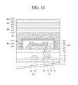
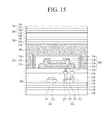
FIGs. 9 to 15 are cross-sectional views illustrating a method for manufacturing an organic light emitting display apparatus according to an embodiment of the present invention. - Reference will now be made in detail to embodiments of the present invention, examples of which are illustrated in the accompanying drawings. Wherever possible, the same reference numbers may be used throughout the drawings to refer to the same or like parts.
- When a structure is formed "on" another structure, it is to be understood that these structures are in contact with each other or that a third structure(s) is interposed between the structures. However, if the terminology "directly on" is used, it is to be understood that these structures are in contact with each other.
-
FIG. 4 briefly illustrates a cross-section of an organic light emitting display (OLED) apparatus according to an embodiment of the present invention. - The OLED apparatus includes a
TFT substrate 100, which includes a thin film transistor, an organiclight emitting element 200, apassivation layer 300 formed on the organiclight emitting element 200 to cover the organiclight emitting element 200, aviscoelastic layer 400 formed on thepassivation layer 300 to cover thepassivation layer 300, and anencapsulation film 500 on theviscoelastic layer 400. - As illustrated in
FIG. 4 , the OLED apparatus may further include a circular polarizingplate 600 on theencapsulation film 500, and afront module 700 on the circular polarizingplate 600. -
FIG. 5 briefly illustrates a cross-section of aTFT substrate 100 according to an embodiment of the present invention. - As illustrated in
FIG. 5 , theTFT substrate 100 includes apolyimide film 110, abuffer layer 120 on one surface of thepolyimide film 110, athin film transistor 130 and acapacitor 140 formed on thebuffer layer 120, and arear plate 190 attached onto another surface of thepolyimide film 110 using anadhesive layer 180. - The
thin film transistor 130 includes asemiconductor layer 131, agate electrode 132, and source anddrain electrodes capacitor 140 includes a capacitorlower electrode 141 and a capacitorupper electrode 142. - A gate
insulating film 150 is formed between thesemiconductor layer 131 and thegate electrode 132 and between the capacitorlower electrode 141 and the capacitorupper electrode 142. An interlayerinsulating film 160 is formed on the capacitorupper electrode 142 and between thegate electrode 132 and the source anddrain electrodes - An
overcoat layer 170 is formed on theinterlayer insulating film 160 and the source anddrain electrodes thin film transistor 130 and thecapacitor 140 and planarize a step difference caused by thethin film transistor 130. - A
first electrode 210 of the organiclight emitting element 200 is electrically connected with thedrain electrode 134 of thethin film transistor 130 through a hole formed in theovercoat layer 170. - Although the
TFT substrate 100 illustrated inFIG. 5 has a structure for a flexible display apparatus and includes a top-gate type thin film transistor where thegate electrode 132 is disposed above thesemiconductor layer 131, the present invention is not limited to such a structure ofFIG. 5 , and theTFT substrate 100 may include a bottom-gate type thin film transistor where the gate electrode is located below the semiconductor layer or have a non-flexible structure. - For example, as illustrated in
FIG. 6 , the TFT substrate 100' includes asubstrate 111 formed of glass or plastic material, agate electrode 113a on thesubstrate 111, a gateinsulating film 112 and thegate electrode 113a, asemiconductor layer 113b overlapped with thegate electrode 113a, with thegate insulating film 112 interposed between thesemiconductor 113b and thegate electrode 113a, source anddrain electrodes gate insulating film 112 and thesemiconductor layer 113b, and an inorganicinsulating film 114 and an organicinsulating film 115 sequentially formed on thesubstrate 111 provided with thethin film transistor 113. Thefirst electrode 210 of the organiclight emitting element 200 is electrically connected with thedrain electrode 113d of thethin film transistor 113 through a hole formed in the inorganicinsulating film 114 and the organic insulatingfilm 115. - Hereinafter, the organic
light emitting element 200 on theTFT substrate 100 according to an embodiment of the present invention will be described in more detail with reference toFIG. 4 . - The organic
light emitting element 200 includes afirst electrode 210 on theTFT substrate 100, abank layer 220 formed on thefirst electrode 210 and having a bank hole to expose at least a part of thefirst electrode 210 corresponding to a light emitting area, a light-emissiveorganic layer 230 on the part of thefirst electrode 210, which is exposed through the bank hole of thebank layer 220, asecond electrode 240 on the light-emissiveorganic layer 230, and acapping layer 250 on thesecond electrode 240. - The
first electrode 210 is electrically connected with the thin film transistor of the TFT substrate 100 (more specifically, electrically connected with the drain electrode 134). Thefirst electrode 210 may be an anode electrode and formed of a transparent conductive material having a high work function, such as indium tin oxide (ITO), indium zinc oxide (IZO), indium tin zinc oxide (ITZO), indium cerium oxide (ICO), or ZnO. - The bank hole of the
bank layer 220 may define the light emitting area by exposing at least a part of thefirst electrode 210. - The light-emissive
organic layer 230 formed on thefirst electrode 210 and a part of thebank layer 220 may include a light emitting layer, a hole injection layer and/or a hole transport layer between thefirst electrode 210 and the light emitting layer, and an electron injection layer and/or an electron transport layer between thesecond electrode 240 and the light emitting layer. - The
second electrode 240 disposed on the light-emissiveorganic layer 230 may be a cathode electrode and formed of metal having a low work function such as Al, Mg, Ca, Ag or their alloy. - The OLED apparatus according to an embodiment of the present invention may be a rear light-emissive type where light emitted from the light-emissive
organic layer 230 passes through theTFT substrate 100 or a front light-emissive type where light emitted from the light-emissiveorganic layer 230 passes through thefront module 700. - In case of the rear light-emissive type OLED apparatus, the
second electrode 240 may have a thickness enough to reflect light. - On the other hand, in case of the front light-emissive type OLED apparatus, the
second electrode 240 may have a thickness thin enough (e.g., 1Å to 50Å) to transmit light, and a reflecting layer (not shown) formed of Al, Ag or Ni may be arranged below thefirst electrode 210. Also, as illustrated inFIG. 4 , thecapping layer 250 may be formed on thesecond electrode 240. Thecapping layer 250 is used to reduce or prevent the light emitted from the light-emissiveorganic layer 230 from being totally reflected above thesecond electrode 240, and may be formed of a mixture of a conductive inorganic material and an organic material. A metal, for example, transition metal, alkali metal, alkali earth metal, rare-earth metal, or their alloy of two or more metals may be used as the conductive inorganic material. An organic material (for example, material that may be used as a host material of the hole transport layer) having excellent hole mobility or an organic material (for example, material that may be used as a host material of the electron transport layer) having excellent electron mobility may be used as the organic material. The conductive inorganic material may increase scattering of light and absorption of light by generating surface Plasmon resonance at thecapping layer 250, and may prevent total reflection from occurring above thesecond electrode 240, whereby light extraction effect of the OLED apparatus is improved. - Meanwhile, as illustrated in
FIG. 4 , the OLED apparatus according to an embodiment of the present invention includes apassivation layer 300 formed on theTFT substrate 100 to cover the organiclight emitting element 200. - The
passivation layer 300 includes a firstinorganic layer 310 formed on theTFT substrate 100 and the organiclight emitting element 200, anorganic layer 320 on the firstinorganic layer 310, and a secondinorganic layer 330 on theorganic layer 320. - The first and second
inorganic layers organic layer 320 may be formed of an organic matter suitable for shielding water/oxygen, such as acryl resin, epoxy resin, polyimide resin, and polyethylene. Theorganic layer 320 serves to reduce stress between the respective layers, which occurs when the OLED apparatus is bent. - The OLED apparatus further includes a
viscoelastic layer 400 formed on theTFT substrate 100 to fully cover thepassivation layer 300, and anencapsulation film 500 on theviscoelastic layer 400. - Hereinafter, the
viscoelastic layer 400 according to an embodiment of the present invention will be described in more detail with reference toFIGs. 7 and 8 . -
FIG. 7 is a Maxwell model of a viscoelastic material, andFIG. 8 is a graph illustrating variation of stress with time of a viscoelastic material measured through a relaxation modulus test. - The
viscoelastic layer 400 is formed of a viscoelastic material that may be displayed as a Maxwell model illustrated inFIG. 7 . As illustrated inFIG. 7 , the viscoelastic material generally includes a dashpot element η and a spring element E. - As illustrated in the graph of
FIG. 8 , if a rapid strain is given to the viscoelastic material at a predetermined temperature through the relaxation modulus test, the spring element E is immediately stretched and at the same time stress σ is generated. However, as time T passes, a strain of the spring element E is offset by the dashpot element η, and stress σ is rapidly reduced and then is converged to a specific value. - The relaxation modulus test is a linear viscoelastic measurement method, which is performed to obtain information on a structure of a material having viscoelasticity. The relaxation modulus test measures variation of stress with the lapse of time when a constant strain is given at a predetermined temperature condition. Namely, stress caused by a stimulus such as a strain, which is given to the material, is measured by a reaction of the material to the stimulus.
- Preferably, the
viscoelastic layer 400 is formed of a viscoelastic material that basically satisfies characteristics, such as water vapor transmissibility of about 10 g/m2/day or less, visible light transmissibility of about 95% or more and a modulus of about 0.3 MPa or less, at the same time. Theviscoelastic layer 400 is used to encapsulate the OLED apparatus. - In addition, the
viscoelastic layer 400 is formed of a viscoelastic material, and its elastic portion (Ep), which is defined by the following Equation 1, is about 30% or more:
- wherein σ0 is initial stress generated when a strain of about 50% is applied to the viscoelastic material and σ is final stress measured after the strain is continuously applied thereto for about 180 seconds, with the initial stress σ0 and the final stress σ being measured at about 80°C through a relaxation modulus test.
- In other words, the elastic portion Ep may be used as a reference for determining whether a certain viscoelastic material is suitable for the encapsulation structure of the OLED apparatus. When the
viscoelastic layer 400 has an elastic portion Ep of about 30% or more, bubbles that might be recognized under an environment of high temperature and high humidity may remarkably be reduced or prevented from occurring. - The
viscoelastic layer 400 may be formed of a viscoelastic material that includes acryl resin, olefin resin, synthetic rubber, or mixture of two or more thereof. - The
encapsulation film 500 formed on theviscoelastic layer 400 may include an optically-isotropic film 540, a firstorganic film 530 on the optically-isotropic film 540, aninorganic film 520 on the firstorganic film 530, and a secondorganic film 510 on theinorganic film 520. The secondorganic film 510 may be directly in contact with theviscoelastic layer 400. - The
inorganic film 520 may be formed of a material that includes one or more of Al2O3, SiO2, Si3N4, SiON, AlON, AlN, TiO2, ZrO, ZnO, and Ta2O5, and the first and secondorganic films organic films - According to one embodiment of the present invention, the
viscoelastic layer 400 and theencapsulation film 500 have a water vapor transmission rate of about 5×10⁻² g/m2/day or less. In order to have the water vapor transmission rate, theencapsulation film 500 may further include additional inorganic film and/or additional organic film. - As illustrated in
FIG. 4 , the OLED apparatus according to one embodiment of the present invention further includes a circularpolarizing plate 600 on theencapsulation film 500, and afront module 700 on the circularpolarizing plate 600. - For adhesion with the circular
polarizing plate 600, theencapsulation film 500 may further include an adhesive film on the optically-isotropic film 540. - Also, for adhesion between the circular
polarizing plate 600 and thefront module 700, the OLED apparatus may further include an adhesive layer (not shown) formed of an adhesive material such as a pressure sensitive adhesive (PSA) and an optically clear adhesive (OCA). - The circular
polarizing plate 600 is used to reduce or prevent visibility deterioration from occurring, which is caused as the external light reflected by the organiclight emitting element 200 is emitted from the OLED apparatus, and may reduce or prevent the external light reflected by thesecond electrode 240 of the organiclight emitting element 200 from being emitted from the OLED apparatus. - The circular
polarizing plate 600 may include a λ/4phase difference film 610 on theencapsulation film 500 and a linearpolarizing film 620 on the λ/4phase difference film 610. The external light becomes the linear polarizing light after passing through the linearpolarizing film 620. The linear polarizing light passes through the λ/4phase difference film 610, is reflected by thesecond electrode 240 and converted to a liner polarizing light vertical to a transmission axis of the linearpolarizing film 620 after passing through again the λ/4phase difference film 610, and then is absorbed by the linearpolarizing film 620. - The λ/4
phase difference film 610 may have a thickness of about 50 µm to about 100 µm and a phase retardation value of about 120 nm to about 148 nm. - In order to effectively reduce or prevent the external light reflected by the
second electrode 240 of the organiclight emitting element 200 from being visible by being emitted from the OLED apparatus, the optically-isotropic film 540 of theencapsulation film 500 may be an isotropic film having a phase retardation value of about 10 nm or less. - The
front module 700 may include atouch film 710 and acover window 720, and may be attached to the circularpolarizing plate 500 using an adhesive layer. The cover window may be formed of glass or plastic. - Hereinafter, a method for manufacturing an OLED apparatus according to an embodiment of the present invention will be described in detail with reference to
FIGs. 9 to 15 . - First of all, as illustrated in
FIG. 9 , after asubstrate 100a that includes athin film transistor 130 is prepared, an organiclight emitting element 200 is formed on thesubstrate 100a. - In order to prepare the
substrate 100a, apolyimide film 110 is formed on aglass substrate 101. Subsequently, abuffer layer 120 of an inorganic material is formed on thepolyimide film 110. - The
semiconductor layer 131 and the capacitorlower electrode 141 are formed to be spaced apart from each other on thebuffer layer 120. Thesemiconductor layer 131 may be amorphous silicon, polysilicon, or oxide semiconductor. - A
gate insulating film 150 is formed on thebuffer layer 120 provided with thesemiconductor layer 131 and the capacitorlower electrode 141. Thegate insulating film 150 may be formed of a silicon oxide film (SiOx) or a silicon nitride film (SiNx). - The
gate electrode 132 and the capacitorupper electrode 142 are respectively formed on thegate insulating film 150 to be respectively overlapped with thesemiconductor layer 131 and the capacitorlower electrode 141. Thegate electrode 132 and the capacitorupper electrode 142 may be formed of Al, Mo, Cr, Au, Ti, Ni, Cu, or their alloy of two or more. - Subsequently, an
interlayer insulating film 160 is formed on thegate insulating film 150 provided with thegate electrode 132 and the capacitorupper electrode 142. Theinterlayer insulating film 160 may be an inorganic single film or an inorganic/organic double film. - The
interlayer insulating film 160 and thegate insulating film 150 may selectively be etched at both sides of thegate electrode 132 interposed between the interlayer insulatingfilm 160 and thegate insulating film 150, whereby two via holes partially exposing thesemiconductor layer 131 are formed. Subsequently, after a metal layer is formed of Al, Mo, Cr, Au, Ti, Ni, Cu or their alloy of two or more on theinterlayer insulating film 160, source and drainelectrodes - An
overcoat layer 170 for passivating thethin film transistor 130 and thecapacitor 140 and planarizing the step difference caused by thethin film transistor 130 is formed on theinterlayer insulating film 160 provided with the source and drainelectrodes overcoat layer 170 may be an inorganic single layer or an inorganic/organic double layer. - In order to form the organic
light emitting element 200 on thesubstrate 100a completed as above, theovercoat layer 170 is selectively etched, whereby a hole for partially exposing thedrain electrode 134 is formed. Subsequently, after a transparent conductive material having a high work function, such as ITO, IZO, ITZO, ICO, or ZnO, is deposited on thesubstrate 100a through a CVD or sputtering process, thefirst electrode 210 is formed by photolithography and etching processes. - In the case that the front light-emissive type OLED apparatus is manufactured, a reflective layer (not shown) may be formed on the
substrate 100a before forming thefirst electrode 210 with metal such as Ag or Ni. - After an organic insulating layer is formed on the
substrate 100a provided with thefirst electrode 210 by using an organic non-conductive material such as benzocyclobutene (BCB), acryl resin, epoxy resin, polyamide resin, and polyimide resin, a selective etching process is performed to etch the organic insulating layer to form abank layer 220 having a bank hole, which exposes at least a part of thefirst electrode 210. - Subsequently, a light-emissive
organic layer 230, asecond electrode 240, and acapping layer 220 are sequentially formed on thebank layer 220 and thefirst electrode 210 by the known methods. - The
second electrode 240 disposed on the light-emissiveorganic layer 230 may be formed of Al, Mg, Ca, Ag or their alloy, which has a low work function. In the case that the rear light-emissive type OLED apparatus is manufactured, thesecond electrode 240 is formed to have a thickness thick enough to reflect light. On the other hand, in the case that the front light-emissive type OLED apparatus is manufactured, thesecond electrode 240 is formed to have a thickness thin enough (e.g., 1Å to 50Å) to transmit light. - The
capping layer 250, which is used to reduce or prevent the light emitted from the light-emissiveorganic layer 230 from being totally reflected above thesecond electrode 240, is formed on thesecond electrode 240. Thecapping layer 250 may have a thickness of about 10 nm to about 100 nm. - As described above, the
capping layer 250 may be formed of a mixture of a conductive inorganic material and an organic material. A metal, for example, transition metal, alkali metal, alkali earth metal, rare-earth metal, or their alloy of two or more metals may be used as the conductive inorganic material. For example, if a nanosilver particle is used as the conductive inorganic material, the nanosilver particle and the organic material are respectively jetted and then deposited on thesecond electrode 240 to form thecapping layer 250, wherein the content of the nanosilver particle contained in thecapping layer 250 may be less than about 10% by weight. - Subsequently, as illustrated in
FIG. 10 , thepassivation layer 300 is formed on thesubstrate 100a to fully cover the organiclight emitting element 200. - The step of forming the
passivation layer 300 includes the steps of forming the firstinorganic layer 310 on theTFT substrate 100 and the organiclight emitting element 200, forming theorganic layer 320 on the firstinorganic layer 310, and forming the secondinorganic layer 330 on theorganic layer 320. - Each of the first and second
inorganic layers organic layer 320 may be formed of an organic matter suitable for shielding water/oxygen, such as acryl resin, epoxy resin, polyimide resin, and polyethylene. - Since the light-emissive
organic layer 230 may be damaged at a high temperature of 110°C or more, it is preferable that the first and secondinorganic layers - The
organic layer 320 may be formed through vapor deposition, coating or printing. - Subsequently, as illustrated in
FIG. 11 , theencapsulation film 500 is attached onto thepassivation layer 300 through theviscoelastic layer 400. Theviscoelastic layer 400 may be a double sided tape. - The
viscoelastic layer 400 according to an embodiment of the present invention, which is interposed between thepassivation layer 300 and theencapsulation film 500, is formed of a viscoelastic material, and its elastic portion, which is defined by Equation 1, is about 30% or more.
- σ0 is initial stress generated when a strain of about 50% is applied to the viscoelastic material and σ is final stress measured after the strain is continuously applied thereto for about 180 seconds. The initial stress σ0 and the final stress σ are measured at about 80°C through a relaxation modulus test.
- As described above, the viscoelastic material may include acrylic resin, olefin resin, synthetic rubber or mixture of two or more thereof, which satisfies various characteristics of the encapsulation structure of the OLED apparatus, that is, water vapor transmissibility of about 10 g/m2/day or less, visible light transmissibility of about 95% or more, and modulus of about 0.3 MPa or less.
- According to one embodiment of the present invention, the first
organic film 530, theinorganic film 520, and the secondorganic film 510 are sequentially deposited on the optically-isotropic film 540, whereby theencapsulation film 500 which is separately formed may be attached to thepassivation layer 300 and theTFT substrate 100 through theviscoelastic layer 400. At this time, the secondorganic film 510 is directly in contact with theviscoelastic layer 400. - The first and second
organic films - The
inorganic film 520 may be formed through a CVD or ALD process, and include an inorganic matter such as Al2O3, SiO2, Si3N4, SiON, AlON, AlN, TiO2, ZrO, ZnO, and Ta2O5, for example. - After adhesion of the
encapsulation film 500, as illustrated inFIG. 12 , the circularpolarizing plate 600, which is separately formed, is attached onto theencapsulation film 500. For adhesion with the circularpolarizing plate 600, theencapsulation film 500 may further include an adhesive film on the optically-isotropic film 540. - The circular
polarizing plate 600 may include a λ/4phase difference film 610 attached onto theencapsulation film 500 and a linearpolarizing film 620 on the λ/4phase difference film 610. - Subsequently, as illustrated in
FIG. 13 , thefront module 700 that includes atouch film 710 and acover window 720 is attached onto the circularpolarizing plate 600. For adhesion between the circularpolarizing plate 600 and thefront module 700, an adhesive such as a pressure sensitive adhesive (PSA) and an optically clear adhesive (OCA) may be used. - Subsequently, as illustrated in
FIG. 14 , theglass substrate 101 which has performed a support function during the manufacturing process may be separated from thepolyimide film 110 using a laser. For ease of separation, a sacrificing layer (not shown), which can be heated and decomposed by absorbing an irradiated laser, may further be formed between theglass substrate 101 and thepolyimide film 110. - Subsequently, as illustrated in
FIG. 15 , after theglass substrate 101 is separated from thepolyimide film 110, arear plate 190 may be attached to thepolyimide film 110 using anadhesive layer 180 such as a pressure sensitive adhesive (PSA) and an optically clear adhesive (OCA) as a support for the OLED apparatus according to an embodiment of the present invention. - Hereinafter, experiment results according to embodiments of the present invention will be described, along with a comparison example, in more detail.
- A relaxation modulus test was carried out by means of the rheometer of ARES (currently, TA Instrument) for viscoelastic materials of a double-sided tape type used to manufacture an encapsulation structure of an OLED apparatus, under the following conditions.
- * Mode : stress relaxation mode
- * Strain: 50%
- * Temperature: 80 °C
- * Duration: 180 seconds
- * Axial force/strain: set to 'disabled'
- Through the relaxation modulus tests, the initial stress σ0 generated when a strain of 50% is applied to the viscoelastic material and the final stress σ after the strain is maintained for 180 seconds were respectively measured, and then the elastic portions (Ep) (%) of the viscoelastic materials were obtained in accordance with the following Equation 1:

- Organic light emitting display apparatuses having the structure of
FIG. 4 were manufactured using viscoelastic materials having elastic portions (Ep) of 30%, 35% and 40% respectively. - An organic light emitting display apparatus having the structure of
FIG. 4 was manufactured using a viscoelastic material having an elastic portion (Ep) of 20%. - A reliability test was performed in accordance with the following method for the OLED apparatuses of the examples 1 to 3 and comparative example, and the results thereof are shown in the following Table 1.
- 10 samples per each apparatus were provided at the high temperature of 80 □ for 180 hours, and then a visual inspection was performed to see whether visually recognizable bubbles had been generated.
[Table 1] Elastic portion (Ep) of viscoelastic material (%) The number of samples where bubble(s) was(were) observed Remark Ex. 1 30 0 - Ex. 2 35 0 - Ex. 3 40 0 - Comp. Ex. 20 4 A total of seven bubbles occurred at four samples - As shown in Table 1, visually recognizable bubbles, which otherwise might be generated under an environment of high temperature and high humidity, are remarkably reduced or prevented when the encapsulation structure is manufactured using the viscoelastic material having an elastic portion (Ep) of 30% or more.
- As described above, visually recognizable bubbles can be remarkably reduced or prevented within an encapsulation structure of an OLED apparatus even under an environment of high temperature and high humidity.
- Accordingly, not only can the productivity of the OLED apparatus be improved, but also the deterioration of the product reliability and damage to the brand image due to the visually recognizable bubbles can be reduced or prevented.
- Also, a reference for determining whether a certain viscoelastic material is suitable for an encapsulation structure of an OLED apparatus may be provided.
- It will be apparent to those skilled in the art that various modifications and variation can be made in the present invention without departing from the spirit or scope of the invention. Thus, it is intended that the present invention cover the modifications and variations of this invention provided they come within the scope of the appended claims and their equivalents.
Claims (15)
- An organic light emitting display (OLED) apparatus, comprising:a substrate;an organic light emitting element on the substrate, the organic light emitting element including a first electrode, an organic light emitting layer and a second electrode;a viscoelastic layer on the organic light emitting element, wherein an elastic portion of the viscoelastic layer is about 30% or more, the elastic portion being defined by Equation 1:

wherein σ0 is an initial stress generated when a strain of about 50% is applied to the viscoelastic layer and σ is a final stress measured after the strain is continuously applied thereto for about 180 seconds, with the initial stress σ0 and the final stress σ being measured at about 80°C through a relaxation modulus test. - The OLED apparatus according to claim 1, further comprising a passivation layer between the organic light emitting element and the viscoelastic layer, wherein the passivation layer has a combination of an organic layer and an inorganic layer.
- The OLED apparatus according to claim 1 and/or claim 2, wherein the viscoelastic layer satisfies at least one of a water vapor transmissibility of about 10 g/m2/day or less, a visible light transmissibility of about 95% or more, and a modulus of about 0.3 MPa or less.
- The OLED apparatus according to any one of claims 1 to 3, wherein the viscoelastic layer includes at least one of acryl resin, olefin resin and synthetic rubber.
- The OLED apparatus according to any one of claims 1 to 4, further comprising an encapsulation film on the viscoelastic layer, preferably further comprising a circular polarizing plate on the encapsulation film, and a touch film on the polarizing plate.
- The OLED apparatus according to claim 5, wherein the encapsulation film has a combination of an organic layer and an inorganic layer.
- The OLED apparatus according to claim 6, wherein the organic layer of the encapsulation film is in contact with the viscoelastic layer and/or wherein the organic layer of the encapsulation film includes at least one of acryl resin, epoxy resin, polyimide resin and polyethylene.
- The OLED apparatus according to claim 6, wherein the inorganic layer of the encapsulation film includes at least one of Al2O3, SiO2, Si3N4, SiON, AlON, AlN, TiO2, ZrO, ZnO and Ta2O5.
- A method for manufacturing an organic light emitting display (OLED) apparatus, the method comprising:forming an organic light emitting element on a first substrate, which includes forming a first electrode, forming an organic light emitting layer and forming a second electrode;forming a viscoelastic layer on the organic light emitting element, wherein an elastic portion of the viscoelastic layer is about 30% or more, with the elastic portion being defined by Equation 1:

wherein σ0 is an initial stress generated when a strain of about 50% is applied to the viscoelastic layer and σ is a final stress measured after the strain is continuously applied thereto for about 180 seconds, with the initial stress σ0 and the final stress σ being measured at about 80°C through a relaxation modulus test. - The method according to claim 9, further comprising forming a passivation layer on the organic light emitting element, which includes forming an organic layer and forming an inorganic layer.
- The method according to claim 9 and/or claim 10, wherein the viscoelastic layer satisfies at least one of a water vapor transmissibility of about 10 g/m2/day or less, a visible light transmissibility of about 95% or more, and a modulus of about 0.3 MPa or less.
- The method according to any one of claims 9 to 11, wherein the viscoelastic layer includes at least one of acryl resin, olefin resin and synthetic rubber.
- The method according to any one of claims 9 to 12, further comprising forming an encapsulation film on the viscoelastic layer and/or further comprising replacing the first substrate with a flexible second substrate.
- The method according to claim 13, wherein the process of forming the encapsulation film includes forming an organic layer and forming an inorganic layer.
- The method according to claim 14, wherein the organic layer of the encapsulation film is directly formed on the viscoelastic layer and/or wherein the organic layer of the encapsulation film includes at least one of acryl resin, epoxy resin, polyimide resin and polyethylene; and/or wherein the inorganic layer of the encapsulation film includes
at least one of Al2O3, SiO2, Si3N4, SiON, AlON, AlN, TiO2, ZrO, ZnO and Ta2O5.
Applications Claiming Priority (1)
| Application Number | Priority Date | Filing Date | Title |
|---|---|---|---|
| KR1020130145331A KR101692351B1 (en) | 2013-11-27 | 2013-11-27 | Organic Light Emitting Display Apparatus and Method for Manufacturing The Same |
Publications (2)
| Publication Number | Publication Date |
|---|---|
| EP2879197A1 true EP2879197A1 (en) | 2015-06-03 |
| EP2879197B1 EP2879197B1 (en) | 2016-09-21 |
Family
ID=51904846
Family Applications (1)
| Application Number | Title | Priority Date | Filing Date |
|---|---|---|---|
| EP14194161.7A Active EP2879197B1 (en) | 2013-11-27 | 2014-11-20 | Organic light emitting display apparatus and method for manufacturing the same |
Country Status (5)
| Country | Link |
|---|---|
| US (1) | US9203051B2 (en) |
| EP (1) | EP2879197B1 (en) |
| JP (1) | JP5976759B2 (en) |
| KR (1) | KR101692351B1 (en) |
| CN (1) | CN104681583B (en) |
Cited By (1)
| Publication number | Priority date | Publication date | Assignee | Title |
|---|---|---|---|---|
| EP3163337A1 (en) * | 2015-10-30 | 2017-05-03 | LG Display Co., Ltd. | Organic light emitting display device |
Families Citing this family (34)
| Publication number | Priority date | Publication date | Assignee | Title |
|---|---|---|---|---|
| KR101814769B1 (en) | 2010-07-07 | 2018-01-04 | 삼성디스플레이 주식회사 | Organic light emitting diode display and manufacturing method thereof |
| KR102347532B1 (en) * | 2014-01-23 | 2022-01-05 | 삼성디스플레이 주식회사 | Flexible display apparatus and method of manufacturing thereof |
| JP6738139B2 (en) * | 2014-11-20 | 2020-08-12 | 日東電工株式会社 | Circularly polarizing plate for organic EL display device and organic EL display device |
| WO2016080431A1 (en) * | 2014-11-20 | 2016-05-26 | 日東電工株式会社 | Circular polarization plate for organic el display device and organic el display device |
| KR102316211B1 (en) * | 2014-11-24 | 2021-10-22 | 삼성디스플레이 주식회사 | Organic light emitting diode display |
| CN104658990B (en) * | 2015-03-02 | 2017-05-17 | 京东方科技集团股份有限公司 | Packaging assembly and preparation method thereof |
| US20160322603A1 (en) * | 2015-04-30 | 2016-11-03 | EverDisplay Optonics (Shanghai) Limited | Display structure and manufacturing method of display device |
| US9947895B2 (en) | 2015-06-17 | 2018-04-17 | Universal Display Corporation | Flexible AMOLED display |
| CN105261712B (en) * | 2015-08-31 | 2017-07-25 | 上海和辉光电有限公司 | A kind of flexible OLED display panel |
| KR102354976B1 (en) * | 2015-09-15 | 2022-01-25 | 삼성디스플레이 주식회사 | Display apparatus |
| CN106068564B (en) * | 2015-10-29 | 2019-10-11 | 京东方科技集团股份有限公司 | Display device and manufacturing method thereof |
| KR102426710B1 (en) * | 2015-11-03 | 2022-07-29 | 삼성디스플레이 주식회사 | Organic light-emitting display apparatus and manufacturing the same |
| KR102472607B1 (en) * | 2016-02-03 | 2022-11-30 | 삼성디스플레이 주식회사 | Display device |
| CN105679964A (en) * | 2016-03-28 | 2016-06-15 | 中国电子科技集团公司第五十五研究所 | Organic light-emitting device (OLED) packaging structure and method |
| JP2017182892A (en) * | 2016-03-28 | 2017-10-05 | セイコーエプソン株式会社 | Light-emitting element, light-emitting device and electronic apparatus |
| KR102563454B1 (en) * | 2016-04-26 | 2023-08-03 | 엘지디스플레이 주식회사 | Pressure sensor integrated organic light emitting display device and touch screen integrated organic light emitting display device |
| WO2017199885A1 (en) * | 2016-05-16 | 2017-11-23 | 凸版印刷株式会社 | Gas barrier retardation film and organic el display |
| KR20170135585A (en) * | 2016-05-31 | 2017-12-08 | 엘지디스플레이 주식회사 | Organic Light Emitting Display device having a bank insulating layer |
| US10147772B2 (en) * | 2016-08-23 | 2018-12-04 | 3M Innovative Properties Company | Foldable OLED device with compatible flexural stiffness of layers |
| WO2018056401A1 (en) * | 2016-09-23 | 2018-03-29 | 凸版印刷株式会社 | Gas barrier optical film and organic el display |
| KR101992915B1 (en) * | 2016-09-30 | 2019-06-25 | 엘지디스플레이 주식회사 | Organic light emitting display with touch sensor and fabricating method thereof |
| KR101992916B1 (en) * | 2016-09-30 | 2019-06-25 | 엘지디스플레이 주식회사 | Organic light emitting display with touch sensor and fabricating method thereof |
| CN106898633B (en) | 2017-02-24 | 2019-09-10 | 深圳市华星光电技术有限公司 | Light emitting diode indicator and preparation method thereof |
| WO2018167602A1 (en) | 2017-03-16 | 2018-09-20 | 株式会社半導体エネルギー研究所 | Method for manufacturing semiconductor device, and semiconductor device |
| CN109599030B (en) * | 2017-09-30 | 2020-12-11 | 昆山国显光电有限公司 | Display screen and electronic product |
| WO2019171826A1 (en) * | 2018-03-05 | 2019-09-12 | 富士フイルム株式会社 | Gas barrier film, optical element, and method for producing gas barrier film |
| CN108364994A (en) * | 2018-04-04 | 2018-08-03 | 深圳市华星光电技术有限公司 | OLED display and preparation method thereof |
| CN109343743A (en) * | 2018-12-07 | 2019-02-15 | 武汉华星光电半导体显示技术有限公司 | Flexible touch display module |
| JP2021043263A (en) * | 2019-09-06 | 2021-03-18 | 富士通オプティカルコンポーネンツ株式会社 | Optical modulation device and method for manufacturing optical modulation device |
| CN111063825A (en) * | 2019-12-09 | 2020-04-24 | 武汉华星光电半导体显示技术有限公司 | Flexible OLED packaging structure, manufacturing method thereof and display device |
| WO2022054018A1 (en) * | 2020-09-11 | 2022-03-17 | Oti Lumionics Inc. | Opto-electronic device including patterned em radiation-absorbing layer |
| US20230413603A1 (en) * | 2020-10-29 | 2023-12-21 | Oti Lumionics Inc. | Opto-electronic device with nanoparticle deposited layers |
| KR102839164B1 (en) * | 2021-10-28 | 2025-07-25 | 엘지디스플레이 주식회사 | Display apparatus |
| CN114141830B (en) * | 2021-11-22 | 2023-05-30 | 深圳市华星光电半导体显示技术有限公司 | Display panel and display device |
Citations (2)
| Publication number | Priority date | Publication date | Assignee | Title |
|---|---|---|---|---|
| JP2007200692A (en) * | 2006-01-26 | 2007-08-09 | Konica Minolta Holdings Inc | Organic electroluminescent panel manufacturing method, organic electroluminescent panel |
| KR20090128301A (en) * | 2008-06-10 | 2009-12-15 | 엘지디스플레이 주식회사 | Organic light emitting diode display device |
Family Cites Families (11)
| Publication number | Priority date | Publication date | Assignee | Title |
|---|---|---|---|---|
| JPH0519306A (en) * | 1991-07-16 | 1993-01-29 | Nippon Sheet Glass Co Ltd | Fully solid-state dimming device and dimming method with the same |
| JP5127103B2 (en) | 2001-09-10 | 2013-01-23 | 株式会社半導体エネルギー研究所 | LIGHT EMITTING DEVICE AND ELECTRONIC DEVICE |
| JP2004095551A (en) | 2002-08-09 | 2004-03-25 | Semiconductor Energy Lab Co Ltd | Light emitting device and its manufacturing method |
| KR100885843B1 (en) * | 2002-08-31 | 2009-02-27 | 엘지디스플레이 주식회사 | Organic light emitting display device and manufacturing method thereof |
| JP4479381B2 (en) * | 2003-09-24 | 2010-06-09 | セイコーエプソン株式会社 | Electro-optical device, method of manufacturing electro-optical device, and electronic apparatus |
| JP2010133987A (en) * | 2007-03-12 | 2010-06-17 | Toagosei Co Ltd | Optical film laminate and display device using the same |
| JP5541849B2 (en) * | 2008-06-23 | 2014-07-09 | エルジー ディスプレイ カンパニー リミテッド | Organic EL display and manufacturing method thereof |
| KR101074801B1 (en) * | 2009-09-09 | 2011-10-19 | 삼성모바일디스플레이주식회사 | Light emitting display device |
| JP4691205B1 (en) * | 2010-09-03 | 2011-06-01 | 日東電工株式会社 | Method for producing optical film laminate including thin high-performance polarizing film |
| JP2013077460A (en) | 2011-09-30 | 2013-04-25 | Toppan Printing Co Ltd | Manufacturing method of organic el panel, organic el panel, and organic el display |
| KR102168722B1 (en) | 2011-11-04 | 2020-10-22 | 린텍 가부시키가이샤 | Gas barrier film, method for producing same, gas barrier film laminate, member for electronic devices, and electronic device |
-
2013
- 2013-11-27 KR KR1020130145331A patent/KR101692351B1/en active Active
-
2014
- 2014-11-07 US US14/535,471 patent/US9203051B2/en active Active
- 2014-11-19 JP JP2014234627A patent/JP5976759B2/en active Active
- 2014-11-19 CN CN201410665690.2A patent/CN104681583B/en active Active
- 2014-11-20 EP EP14194161.7A patent/EP2879197B1/en active Active
Patent Citations (2)
| Publication number | Priority date | Publication date | Assignee | Title |
|---|---|---|---|---|
| JP2007200692A (en) * | 2006-01-26 | 2007-08-09 | Konica Minolta Holdings Inc | Organic electroluminescent panel manufacturing method, organic electroluminescent panel |
| KR20090128301A (en) * | 2008-06-10 | 2009-12-15 | 엘지디스플레이 주식회사 | Organic light emitting diode display device |
Cited By (2)
| Publication number | Priority date | Publication date | Assignee | Title |
|---|---|---|---|---|
| EP3163337A1 (en) * | 2015-10-30 | 2017-05-03 | LG Display Co., Ltd. | Organic light emitting display device |
| US10283735B2 (en) | 2015-10-30 | 2019-05-07 | Lg Display Co., Ltd. | Organic light emitting display device |
Also Published As
| Publication number | Publication date |
|---|---|
| EP2879197B1 (en) | 2016-09-21 |
| US20150144909A1 (en) | 2015-05-28 |
| KR20150061338A (en) | 2015-06-04 |
| JP5976759B2 (en) | 2016-08-24 |
| CN104681583A (en) | 2015-06-03 |
| CN104681583B (en) | 2017-11-28 |
| JP2015103525A (en) | 2015-06-04 |
| US9203051B2 (en) | 2015-12-01 |
| KR101692351B1 (en) | 2017-01-03 |
Similar Documents
| Publication | Publication Date | Title |
|---|---|---|
| EP2879197B1 (en) | Organic light emitting display apparatus and method for manufacturing the same | |
| US10790460B2 (en) | Organic light-emitting display device | |
| US10236472B2 (en) | Light-emitting device with transparent substrate | |
| KR102568167B1 (en) | Flexible window and flexible display device comprising the same | |
| JP2011248072A (en) | Method of manufacturing image display device | |
| US10522782B2 (en) | Flexible window and flexible display device including the same | |
| JP2015103522A (en) | Organic light emitting display apparatus and method of manufacturing the same | |
| KR20150049189A (en) | Organic light emitting display, method of fabricating the same | |
| US9519368B2 (en) | Touch screen panel and method of manufacturing the same | |
| TW201114028A (en) | Organic light emitting display device and manufacturing method thereof | |
| KR101842134B1 (en) | Electrophoretic Display Device and Method for Manufacturing The Same | |
| US20180246603A1 (en) | Film touch sensor | |
| US20210408408A1 (en) | Oled display panel and oled display device | |
| KR102109743B1 (en) | Organic Light Emitting Display Apparatus and Method for Manufacturing The Same | |
| US20200083259A1 (en) | Array substrate, method for fabricating array substrate, and display | |
| KR102928629B1 (en) | Window module and display device including the same | |
| US11850823B2 (en) | Electronic device and method for manufacturing the same | |
| US20180198086A1 (en) | Display panel, display apparatus having the same, and fabricating method thereof | |
| US20260042235A1 (en) | Apparatus and method for manufacturing display device and electronic device including display device | |
| KR20150070663A (en) | Organic electro luminescent device having touch screen and method of fabricating the same | |
| EP2124096A1 (en) | Liquid crystal display device, and its manufacturing method | |
| CN107340619A (en) | The manufacture method and detection means of display device |
Legal Events
| Date | Code | Title | Description |
|---|---|---|---|
| PUAI | Public reference made under article 153(3) epc to a published international application that has entered the european phase |
Free format text: ORIGINAL CODE: 0009012 |
|
| 17P | Request for examination filed |
Effective date: 20141120 |
|
| AK | Designated contracting states |
Kind code of ref document: A1 Designated state(s): AL AT BE BG CH CY CZ DE DK EE ES FI FR GB GR HR HU IE IS IT LI LT LU LV MC MK MT NL NO PL PT RO RS SE SI SK SM TR |
|
| AX | Request for extension of the european patent |
Extension state: BA ME |
|
| R17P | Request for examination filed (corrected) |
Effective date: 20151117 |
|
| RBV | Designated contracting states (corrected) |
Designated state(s): AL AT BE BG CH CY CZ DE DK EE ES FI FR GB GR HR HU IE IS IT LI LT LU LV MC MK MT NL NO PL PT RO RS SE SI SK SM TR |
|
| GRAP | Despatch of communication of intention to grant a patent |
Free format text: ORIGINAL CODE: EPIDOSNIGR1 |
|
| INTG | Intention to grant announced |
Effective date: 20160321 |
|
| RAP1 | Party data changed (applicant data changed or rights of an application transferred) |
Owner name: LG DISPLAY CO., LTD. |
|
| GRAS | Grant fee paid |
Free format text: ORIGINAL CODE: EPIDOSNIGR3 |
|
| GRAJ | Information related to disapproval of communication of intention to grant by the applicant or resumption of examination proceedings by the epo deleted |
Free format text: ORIGINAL CODE: EPIDOSDIGR1 |
|
| GRAL | Information related to payment of fee for publishing/printing deleted |
Free format text: ORIGINAL CODE: EPIDOSDIGR3 |
|
| GRAR | Information related to intention to grant a patent recorded |
Free format text: ORIGINAL CODE: EPIDOSNIGR71 |
|
| INTC | Intention to grant announced (deleted) | ||
| GRAA | (expected) grant |
Free format text: ORIGINAL CODE: 0009210 |
|
| INTG | Intention to grant announced |
Effective date: 20160804 |
|
| AK | Designated contracting states |
Kind code of ref document: B1 Designated state(s): AL AT BE BG CH CY CZ DE DK EE ES FI FR GB GR HR HU IE IS IT LI LT LU LV MC MK MT NL NO PL PT RO RS SE SI SK SM TR |
|
| REG | Reference to a national code |
Ref country code: GB Ref legal event code: FG4D |
|
| REG | Reference to a national code |
Ref country code: CH Ref legal event code: EP |
|
| REG | Reference to a national code |
Ref country code: NL Ref legal event code: FP |
|
| REG | Reference to a national code |
Ref country code: AT Ref legal event code: REF Ref document number: 831671 Country of ref document: AT Kind code of ref document: T Effective date: 20161015 |
|
| REG | Reference to a national code |
Ref country code: IE Ref legal event code: FG4D |
|
| REG | Reference to a national code |
Ref country code: DE Ref legal event code: R096 Ref document number: 602014003812 Country of ref document: DE |
|
| REG | Reference to a national code |
Ref country code: FR Ref legal event code: PLFP Year of fee payment: 3 |
|
| REG | Reference to a national code |
Ref country code: LT Ref legal event code: MG4D |
|
| PG25 | Lapsed in a contracting state [announced via postgrant information from national office to epo] |
Ref country code: FI Free format text: LAPSE BECAUSE OF FAILURE TO SUBMIT A TRANSLATION OF THE DESCRIPTION OR TO PAY THE FEE WITHIN THE PRESCRIBED TIME-LIMIT Effective date: 20160921 Ref country code: LT Free format text: LAPSE BECAUSE OF FAILURE TO SUBMIT A TRANSLATION OF THE DESCRIPTION OR TO PAY THE FEE WITHIN THE PRESCRIBED TIME-LIMIT Effective date: 20160921 Ref country code: NO Free format text: LAPSE BECAUSE OF FAILURE TO SUBMIT A TRANSLATION OF THE DESCRIPTION OR TO PAY THE FEE WITHIN THE PRESCRIBED TIME-LIMIT Effective date: 20161221 Ref country code: RS Free format text: LAPSE BECAUSE OF FAILURE TO SUBMIT A TRANSLATION OF THE DESCRIPTION OR TO PAY THE FEE WITHIN THE PRESCRIBED TIME-LIMIT Effective date: 20160921 |
|
| REG | Reference to a national code |
Ref country code: AT Ref legal event code: MK05 Ref document number: 831671 Country of ref document: AT Kind code of ref document: T Effective date: 20160921 |
|
| PG25 | Lapsed in a contracting state [announced via postgrant information from national office to epo] |
Ref country code: GR Free format text: LAPSE BECAUSE OF FAILURE TO SUBMIT A TRANSLATION OF THE DESCRIPTION OR TO PAY THE FEE WITHIN THE PRESCRIBED TIME-LIMIT Effective date: 20161222 Ref country code: BE Free format text: LAPSE BECAUSE OF NON-PAYMENT OF DUE FEES Effective date: 20161130 Ref country code: LV Free format text: LAPSE BECAUSE OF FAILURE TO SUBMIT A TRANSLATION OF THE DESCRIPTION OR TO PAY THE FEE WITHIN THE PRESCRIBED TIME-LIMIT Effective date: 20160921 Ref country code: SE Free format text: LAPSE BECAUSE OF FAILURE TO SUBMIT A TRANSLATION OF THE DESCRIPTION OR TO PAY THE FEE WITHIN THE PRESCRIBED TIME-LIMIT Effective date: 20160921 |
|
| PG25 | Lapsed in a contracting state [announced via postgrant information from national office to epo] |
Ref country code: RO Free format text: LAPSE BECAUSE OF FAILURE TO SUBMIT A TRANSLATION OF THE DESCRIPTION OR TO PAY THE FEE WITHIN THE PRESCRIBED TIME-LIMIT Effective date: 20160921 Ref country code: EE Free format text: LAPSE BECAUSE OF FAILURE TO SUBMIT A TRANSLATION OF THE DESCRIPTION OR TO PAY THE FEE WITHIN THE PRESCRIBED TIME-LIMIT Effective date: 20160921 |
|
| PG25 | Lapsed in a contracting state [announced via postgrant information from national office to epo] |
Ref country code: ES Free format text: LAPSE BECAUSE OF FAILURE TO SUBMIT A TRANSLATION OF THE DESCRIPTION OR TO PAY THE FEE WITHIN THE PRESCRIBED TIME-LIMIT Effective date: 20160921 Ref country code: CZ Free format text: LAPSE BECAUSE OF FAILURE TO SUBMIT A TRANSLATION OF THE DESCRIPTION OR TO PAY THE FEE WITHIN THE PRESCRIBED TIME-LIMIT Effective date: 20160921 Ref country code: BE Free format text: LAPSE BECAUSE OF FAILURE TO SUBMIT A TRANSLATION OF THE DESCRIPTION OR TO PAY THE FEE WITHIN THE PRESCRIBED TIME-LIMIT Effective date: 20160921 Ref country code: PT Free format text: LAPSE BECAUSE OF FAILURE TO SUBMIT A TRANSLATION OF THE DESCRIPTION OR TO PAY THE FEE WITHIN THE PRESCRIBED TIME-LIMIT Effective date: 20170123 Ref country code: SK Free format text: LAPSE BECAUSE OF FAILURE TO SUBMIT A TRANSLATION OF THE DESCRIPTION OR TO PAY THE FEE WITHIN THE PRESCRIBED TIME-LIMIT Effective date: 20160921 Ref country code: BG Free format text: LAPSE BECAUSE OF FAILURE TO SUBMIT A TRANSLATION OF THE DESCRIPTION OR TO PAY THE FEE WITHIN THE PRESCRIBED TIME-LIMIT Effective date: 20161221 Ref country code: SM Free format text: LAPSE BECAUSE OF FAILURE TO SUBMIT A TRANSLATION OF THE DESCRIPTION OR TO PAY THE FEE WITHIN THE PRESCRIBED TIME-LIMIT Effective date: 20160921 Ref country code: PL Free format text: LAPSE BECAUSE OF FAILURE TO SUBMIT A TRANSLATION OF THE DESCRIPTION OR TO PAY THE FEE WITHIN THE PRESCRIBED TIME-LIMIT Effective date: 20160921 Ref country code: IS Free format text: LAPSE BECAUSE OF FAILURE TO SUBMIT A TRANSLATION OF THE DESCRIPTION OR TO PAY THE FEE WITHIN THE PRESCRIBED TIME-LIMIT Effective date: 20170121 Ref country code: AT Free format text: LAPSE BECAUSE OF FAILURE TO SUBMIT A TRANSLATION OF THE DESCRIPTION OR TO PAY THE FEE WITHIN THE PRESCRIBED TIME-LIMIT Effective date: 20160921 |
|
| REG | Reference to a national code |
Ref country code: DE Ref legal event code: R097 Ref document number: 602014003812 Country of ref document: DE |
|
| PG25 | Lapsed in a contracting state [announced via postgrant information from national office to epo] |
Ref country code: IT Free format text: LAPSE BECAUSE OF FAILURE TO SUBMIT A TRANSLATION OF THE DESCRIPTION OR TO PAY THE FEE WITHIN THE PRESCRIBED TIME-LIMIT Effective date: 20160921 |
|
| PLBE | No opposition filed within time limit |
Free format text: ORIGINAL CODE: 0009261 |
|
| STAA | Information on the status of an ep patent application or granted ep patent |
Free format text: STATUS: NO OPPOSITION FILED WITHIN TIME LIMIT |
|
| PG25 | Lapsed in a contracting state [announced via postgrant information from national office to epo] |
Ref country code: DK Free format text: LAPSE BECAUSE OF FAILURE TO SUBMIT A TRANSLATION OF THE DESCRIPTION OR TO PAY THE FEE WITHIN THE PRESCRIBED TIME-LIMIT Effective date: 20160921 |
|
| REG | Reference to a national code |
Ref country code: IE Ref legal event code: MM4A |
|
| 26N | No opposition filed |
Effective date: 20170622 |
|
| REG | Reference to a national code |
Ref country code: FR Ref legal event code: PLFP Year of fee payment: 4 |
|
| PG25 | Lapsed in a contracting state [announced via postgrant information from national office to epo] |
Ref country code: LU Free format text: LAPSE BECAUSE OF NON-PAYMENT OF DUE FEES Effective date: 20161130 |
|
| PG25 | Lapsed in a contracting state [announced via postgrant information from national office to epo] |
Ref country code: SI Free format text: LAPSE BECAUSE OF FAILURE TO SUBMIT A TRANSLATION OF THE DESCRIPTION OR TO PAY THE FEE WITHIN THE PRESCRIBED TIME-LIMIT Effective date: 20160921 Ref country code: IE Free format text: LAPSE BECAUSE OF NON-PAYMENT OF DUE FEES Effective date: 20161120 |
|
| PG25 | Lapsed in a contracting state [announced via postgrant information from national office to epo] |
Ref country code: HU Free format text: LAPSE BECAUSE OF FAILURE TO SUBMIT A TRANSLATION OF THE DESCRIPTION OR TO PAY THE FEE WITHIN THE PRESCRIBED TIME-LIMIT; INVALID AB INITIO Effective date: 20141120 |
|
| PG25 | Lapsed in a contracting state [announced via postgrant information from national office to epo] |
Ref country code: HR Free format text: LAPSE BECAUSE OF FAILURE TO SUBMIT A TRANSLATION OF THE DESCRIPTION OR TO PAY THE FEE WITHIN THE PRESCRIBED TIME-LIMIT Effective date: 20160921 Ref country code: MC Free format text: LAPSE BECAUSE OF FAILURE TO SUBMIT A TRANSLATION OF THE DESCRIPTION OR TO PAY THE FEE WITHIN THE PRESCRIBED TIME-LIMIT Effective date: 20160921 Ref country code: MK Free format text: LAPSE BECAUSE OF FAILURE TO SUBMIT A TRANSLATION OF THE DESCRIPTION OR TO PAY THE FEE WITHIN THE PRESCRIBED TIME-LIMIT Effective date: 20160921 Ref country code: CY Free format text: LAPSE BECAUSE OF FAILURE TO SUBMIT A TRANSLATION OF THE DESCRIPTION OR TO PAY THE FEE WITHIN THE PRESCRIBED TIME-LIMIT Effective date: 20160921 |
|
| PG25 | Lapsed in a contracting state [announced via postgrant information from national office to epo] |
Ref country code: LI Free format text: LAPSE BECAUSE OF NON-PAYMENT OF DUE FEES Effective date: 20171130 Ref country code: CH Free format text: LAPSE BECAUSE OF NON-PAYMENT OF DUE FEES Effective date: 20171130 |
|
| REG | Reference to a national code |
Ref country code: FR Ref legal event code: PLFP Year of fee payment: 5 |
|
| PG25 | Lapsed in a contracting state [announced via postgrant information from national office to epo] |
Ref country code: MT Free format text: LAPSE BECAUSE OF NON-PAYMENT OF DUE FEES Effective date: 20161120 |
|
| PG25 | Lapsed in a contracting state [announced via postgrant information from national office to epo] |
Ref country code: AL Free format text: LAPSE BECAUSE OF FAILURE TO SUBMIT A TRANSLATION OF THE DESCRIPTION OR TO PAY THE FEE WITHIN THE PRESCRIBED TIME-LIMIT Effective date: 20160921 Ref country code: TR Free format text: LAPSE BECAUSE OF FAILURE TO SUBMIT A TRANSLATION OF THE DESCRIPTION OR TO PAY THE FEE WITHIN THE PRESCRIBED TIME-LIMIT Effective date: 20160921 |
|
| REG | Reference to a national code |
Ref country code: DE Ref legal event code: R079 Ref document number: 602014003812 Country of ref document: DE Free format text: PREVIOUS MAIN CLASS: H01L0051520000 Ipc: H10K0050800000 |
|
| PGFP | Annual fee paid to national office [announced via postgrant information from national office to epo] |
Ref country code: NL Payment date: 20250922 Year of fee payment: 12 |
|
| PGFP | Annual fee paid to national office [announced via postgrant information from national office to epo] |
Ref country code: GB Payment date: 20250922 Year of fee payment: 12 |
|
| PGFP | Annual fee paid to national office [announced via postgrant information from national office to epo] |
Ref country code: FR Payment date: 20250925 Year of fee payment: 12 |
|
| PGFP | Annual fee paid to national office [announced via postgrant information from national office to epo] |
Ref country code: DE Payment date: 20250922 Year of fee payment: 12 |