EP2879177A1 - Method for producing sos substrates, and sos substrate - Google Patents
Method for producing sos substrates, and sos substrate Download PDFInfo
- Publication number
- EP2879177A1 EP2879177A1 EP13823217.8A EP13823217A EP2879177A1 EP 2879177 A1 EP2879177 A1 EP 2879177A1 EP 13823217 A EP13823217 A EP 13823217A EP 2879177 A1 EP2879177 A1 EP 2879177A1
- Authority
- EP
- European Patent Office
- Prior art keywords
- substrate
- sos
- sapphire substrate
- silicon
- sapphire
- Prior art date
- Legal status (The legal status is an assumption and is not a legal conclusion. Google has not performed a legal analysis and makes no representation as to the accuracy of the status listed.)
- Granted
Links
Images
Classifications
-
- H—ELECTRICITY
- H10—SEMICONDUCTOR DEVICES; ELECTRIC SOLID-STATE DEVICES NOT OTHERWISE PROVIDED FOR
- H10P—GENERIC PROCESSES OR APPARATUS FOR THE MANUFACTURE OR TREATMENT OF DEVICES COVERED BY CLASS H10
- H10P90/00—Preparation of wafers not covered by a single main group of this subclass, e.g. wafer reinforcement
- H10P90/19—Preparing inhomogeneous wafers
- H10P90/1904—Preparing vertically inhomogeneous wafers
- H10P90/1906—Preparing SOI wafers
- H10P90/1914—Preparing SOI wafers using bonding
- H10P90/1916—Preparing SOI wafers using bonding with separation or delamination along an ion implanted layer, e.g. Smart-cut
-
- H—ELECTRICITY
- H10—SEMICONDUCTOR DEVICES; ELECTRIC SOLID-STATE DEVICES NOT OTHERWISE PROVIDED FOR
- H10D—INORGANIC ELECTRIC SEMICONDUCTOR DEVICES
- H10D30/00—Field-effect transistors [FET]
- H10D30/60—Insulated-gate field-effect transistors [IGFET]
- H10D30/67—Thin-film transistors [TFT]
- H10D30/6758—Thin-film transistors [TFT] characterised by the insulating substrates
- H10D30/6759—Silicon-on-sapphire [SOS] substrates
-
- H—ELECTRICITY
- H10—SEMICONDUCTOR DEVICES; ELECTRIC SOLID-STATE DEVICES NOT OTHERWISE PROVIDED FOR
- H10D—INORGANIC ELECTRIC SEMICONDUCTOR DEVICES
- H10D86/00—Integrated devices formed in or on insulating or conducting substrates, e.g. formed in silicon-on-insulator [SOI] substrates or on stainless steel or glass substrates
- H10D86/01—Manufacture or treatment
- H10D86/03—Manufacture or treatment wherein the substrate comprises sapphire, e.g. silicon-on-sapphire [SOS]
-
- H—ELECTRICITY
- H10—SEMICONDUCTOR DEVICES; ELECTRIC SOLID-STATE DEVICES NOT OTHERWISE PROVIDED FOR
- H10W—GENERIC PACKAGES, INTERCONNECTIONS, CONNECTORS OR OTHER CONSTRUCTIONAL DETAILS OF DEVICES COVERED BY CLASS H10
- H10W10/00—Isolation regions in semiconductor bodies between components of integrated devices
- H10W10/10—Isolation regions comprising dielectric materials
- H10W10/181—Semiconductor-on-insulator [SOI] isolation regions, e.g. buried oxide regions of SOI wafers
Definitions
- This invention relates to a method for producing an SOS substrate by forming a single crystal silicon layer on a sapphire substrate by the bonding technique, and an SOS substrate which is produced by the method, is inexpensive and free of metal contaminants, and has a single crystal silicon layer with less defects.
- hybrid substrates typically silicon-on-sapphire (SOS) substrates based on support substrates of sapphire having characteristics including good insulation, a high thermal conductivity, and a low loss in the radio-frequency band are used to construct devices for radio-frequency applications.
- SOS silicon-on-sapphire
- Patent Document 2 describes that a sapphire substrate of C face is low anisotropic and effective for improving the in-plane uniformity of device properties. Also pointed out therein is the advantage that since C-face sapphire substrates are often used in optical devices such as LEDs, they are available at lower cost than R-face sapphire substrates and contribute to the cost reduction of SOS substrates and devices using the same.
- Non-Patent Document 1 Yoshii et al., Japanese Journal of Applied Physics, Vol. 21, Supplement 21-1, pp.175-179 (1982 )
- sapphire substrates themselves have a high metal concentration, especially high Fe concentration at their surface.
- Typical sapphire substrates have a Fe concentration of 1 ⁇ 10 11 to 1 ⁇ 10 12 atoms/cm 2 , which is higher by one or two orders than the concentration of 1 ⁇ 10 10 atoms/cm 2 required for silicon devices or the like.
- the metal concentration may be reduced, for example, by cleaning with solution SC-2 (HCl+H 2 O 2 +H 2 O) used in the cleaning of silicon wafers. Even after cleaning, however, the metal concentration of sapphire substrates is not so reduced. Cleaning must be repeated to clear the level of 1 ⁇ 10 10 atoms/cm 2 , giving rise to the problem of increased cost and time for cleaning.
- Certain sapphire substrates have the drawback that the Fe concentration is not reduced even by repetition of cleaning.
- An object of the invention which has been made under the above-mentioned circumstances, is to provide a method for producing an SOS substrate having a reduced, uniform number of defects and ready for use in the semiconductor manufacture line, in a reproducible manner, and an SOS substrate produced by the method.
- the inventors have found that the number of defects in a single crystal silicon film varies with the magnitude of an off-angle of a C-face sapphire substrate, the main cause for such variation is face orientation, and it is very important to maintain the face orientation below a certain range.
- the inventors have found that if the magnitude of off-angle exceeds 1°, then the number of defects in a single crystal silicon film increases; and that when the off-angle of a C-face sapphire substrate used is set equal to or below 1°, an SOS substrate having a reduced, invariant number of defects can be produced in a reproducible manner.
- the inventors have found that when the sapphire substrate is heat treated in a reducing atmosphere, especially a hydrogen-containing atmosphere, the concentration of metal impurities at the surface of the sapphire substrate can be substantially reduced.
- the preparation of SOS substrates by the bonding method the inventors have found that when the heat treated sapphire substrate is used, the contamination of the process line is minimized, and the number of defects on a silicon thin film, which has been transferred to the sapphire substrate, is dramatically reduced as compared with the use of untreated substrate. The invention is predicated on these findings.
- Patent Document 3 JP-A H11-74562 , for example, that when a nitride semiconductor layer is formed by hetero-epitaxial growth, an off-angled surface is intentionally formed for the purpose of improving crystallinity.
- an off-angle is not obvious at all when a single crystal film is transferred by the bonding method as in the invention.
- the heat treatment is effective for reducing the number of defects in a silicon layer formed on the sapphire support substrate. That is, it is important that the heat treatment of a sapphire substrate in a hydrogen-containing atmosphere precede the bonding step. As long as the heat treatment precedes, it is successful in removing metal impurities and additionally effective for removing foreign particles of organic matter or the like. As a result, the number of defects after bonding is reduced.
- the invention provides a method for producing an SOS substrate and an SOS substrate, as defined below.
- a C-face sapphire substrate whose face orientation is a C-face having an off-angle of up to 1° is bonded to a silicon substrate, an SOS substrate having a reduced, uniform number of defects in a silicon layer can be produced.
- a sapphire substrate is heat treated in a reducing atmosphere before it is bonded to a silicon substrate, the number of defects in a silicon layer is further reduced, and metal impurities are removed from the sapphire substrate to a level ready for use in the semiconductor manufacture line, without a need for cleaning.
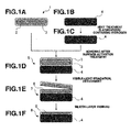
- FIGS. 1A to 1F are a schematic view showing steps of the method for producing an SOS substrate according to one embodiment of the invention
- FIG. 1A being a cross-sectional view of an ion-implanted silicon substrate
- FIG. 1B being a cross-sectional view of a sapphire substrate
- FIG. 1C being a cross-sectional view of the sapphire substrate which has been heat treated in a hydrogen atmosphere
- FIG. 1D being a cross-sectional view of a bonded structure of silicon substrate/sapphire substrate
- FIG. 1E being a cross-sectional view of the structure from which the silicon substrate is separated along the ion-implanted region
- FIG. 1F being a cross-sectional view of an SOS substrate.
- the method for producing an SOS substrate according to the invention involves, as shown in FIGS. 1A to 1F , the following successive steps: step 1 of implanting hydrogen ions (rare gas ions) into a silicon substrate, step 2 of heat treating a sapphire substrate in a hydrogen atmosphere, step 3 of surface activating the silicon substrate and/or sapphire substrate, step 4 of bonding the silicon substrate to the sapphire substrate, step 5 of irradiating visible light and separating, and step 6 of thinning a silicon layer.
- step 1 of implanting hydrogen ions (rare gas ions) into a silicon substrate step 2 of heat treating a sapphire substrate in a hydrogen atmosphere
- step 3 of surface activating the silicon substrate and/or sapphire substrate
- step 4 of bonding the silicon substrate to the sapphire substrate step 5 of irradiating visible light and separating
- step 6 of thinning a silicon layer.
- Step 1 implanting hydrogen ions (rare gas ions) into silicon substrate
- hydrogen ions or rare gas (i.e. helium, neon, argon, krypton, xenon or radon) ions are implanted into a single crystal silicon substrate (donor substrate) 1 from its surface to form a laminar ion-implanted region 3 (also referred to as ion-implanted layer) in the substrate ( FIG. 1A ).
- rare gas i.e. helium, neon, argon, krypton, xenon or radon
- the single crystal silicon substrate 1 (also referred to as silicon substrate, hereinafter) used as the semiconductor substrate may be, for example, a substrate obtained by slicing a single crystal ingot grown by the Czochralski (CZ) method and typically having a diameter of 100 to 300 mm, a conductivity type: P or N type, and a resistivity of about 10 ⁇ cm, but not limited thereto.
- CZ Czochralski
- a thin insulating film 2 may previously be formed on the surface of silicon substrate 1. This is because when ions are implanted through the insulating film 2, an effect of suppressing channeling of implanting ions is obtainable.
- the insulating film 2 preferably has a thickness of up to 300 nm, more preferably up to 50 nm, and even more preferably up to 20 nm. If the thickness of insulating film 2 exceeds 300 nm, the insulating film 2 is liable to crack or peel, due to a difference in coefficient of thermal expansion from sapphire and silicon, during treatment of the SOS substrate at high temperature. Also, when SiO 2 is used as the insulating film 2, its thermal conductivity is low, and its poor heat dissipation becomes a problem when high-power devices are fabricated.
- an oxynitride or nitride having a higher thermal conductivity than SiO 2 for example, Si 3 N 4 may be used as the insulating film 2.
- the lower limit of the thickness of insulating film 2 is not particularly specified, a thickness of at least 20 nm is preferred for the purpose of suppressing void formation during the manufacture of SOS substrates.
- the method of forming the ion-implanted region 3 is not particularly limited.
- a predetermined dose of hydrogen ions or rare gas ions are implanted with an implantation energy sufficient to form the ion-implanted region 3 at the desired depth from the surface of silicon substrate 1.
- Implantation conditions include, for example, an implantation energy of 50 to 100 keV and an implantation dose of 2 ⁇ 10 16 to 1 ⁇ 10 17 /cm 2 .
- Hydrogen ions to be implanted are preferably hydrogen ions (H + ) in a dose of 2 ⁇ 10 16 to 1 ⁇ 10 17 atoms/cm 2 or hydrogen molecule ions (H 2 + ) in a dose of 1 ⁇ 10 16 to 5 ⁇ 10 16 atoms/cm 2 .
- Most preferred are hydrogen ions (H + ) in a dose of 8.0 ⁇ 10 16 atoms/cm 2 or hydrogen molecule ions (H 2 + ) in a dose of 4.0 ⁇ 10 16 atoms/cm 2 .
- the depth from the substrate surface subject to ion implantation to the ion-implanted region 3 corresponds to the desired thickness of a silicon thin film to be formed on the sapphire substrate serving as the support substrate
- the depth of ion implantation is preferably 300 to 500 nm, more preferably about 400 nm.
- the thickness of the ion-implanted region 3 may be sufficient to facilitate separation or exfoliation by mechanical impacts or the like, and is preferably 200 to 400 nm, more preferably about 300 nm.
- Step 2 heat treating sapphire substrate in hydrogen atmosphere
- the sapphire substrate 4 is previously heat treated in a reducing atmosphere ( FIGS. 1B and 1C ).
- the sapphire substrate 4 is an insulating transparent substrate serving as the support substrate or handle substrate for the SOS substrate and specifically, a C-face sapphire substrate whose face orientation is a C-face having an off-angle of up to 1° ( FIG. 1B ). That is, single crystal sapphire of which the sapphire substrate 4 is constructed has a crystal face (0001) or C-face which is parallel to the main surface of the substrate and an off-angle, indicative of an inclination of c-axis among crystal axes relative to the main surface of the substrate, which is up to 1°, preferably up to 0.6°.
- the off-angle is more than 1°, then the number of defects in a single crystal silicon layer in the SOS substrate to be described later is increased, or the variation of the number of defects becomes wider, and the film is liable to peel.
- the sapphire substrate 4 causes less energy loss of light in the visible band (wavelength 400-700 nm) until reaching the ion-implanted region 3 in the silicon substrate 1 bonded thereto.
- a substrate having a transmittance of at least 70% in the visible band is preferred.
- Suitable reducing atmospheres include, for example, a reducing gas of a species selected from carbon monoxide, hydrogen sulfide, sulfur dioxide, hydrogen and formaldehyde, or a combination thereof, and an atmosphere composed of a mixture of the reducing gas with an inert gas.
- a reducing gas of a species selected from carbon monoxide, hydrogen sulfide, sulfur dioxide, hydrogen and formaldehyde, or a combination thereof and an atmosphere composed of a mixture of the reducing gas with an inert gas.
- an atmosphere containing at least hydrogen that is, an atmosphere of hydrogen alone or hydrogen-containing inert gas is preferred, and an atmosphere of hydrogen alone is more preferred.
- the lower limit of the heat treatment temperature is preferably at least 600°C, more preferably at least 700°C. If the heat treatment temperature is below 600°C, the effect of removing metal from the surface of sapphire substrate 4 and the effect of reducing the number of defects on the surface of silicon thin film may be insufficient.
- the upper limit of the heat treatment temperature is preferably up to 1,100°C, more preferably up to 1,000°C, even more preferably up to 900°C. If the heat treatment temperature exceeds 1,100°C, the number of defects on the surface of silicon thin film in the SOS substrate may be rather increased, which is inadequate for the SOS substrate.
- the heat treatment time is preferably 10 seconds to 12 hours, more preferably 1 minute to 1 hour. If the heat treatment time is less than 10 seconds, the removal of metal from the surface of sapphire substrate 4 may be insufficient, or the number of defects on the surface of silicon thin film in the SOS substrate may be insufficiently reduced. If the heat treatment time exceeds 12 hours, the cost of heat treatment may increase.
- the furnace for heat treatment is not particularly limited as long as hydrogen can be introduced in the furnace to establish a reducing atmosphere.
- a tubular furnace, an epitaxial growth furnace, and a rapid thermal annealing (RTA) furnace may be used.
- the metal concentration on the surface of sapphire substrate 4 is reduced from the initial, for example, to or below 1 ⁇ 10 10 atoms/cm 2 ( FIG. 1C ). Also, the heat treatment in the range does not exacerbate the surface roughness of sapphire substrate 4 or interfere with bonding of sapphire substrate 4 to silicon substrate 1.
- Step 3 surface activation of silicon substrate and/or sapphire substrate
- one or both of the surface of the silicon substrate 1 subject to ion implantation and the surface of the heat treated sapphire substrate 4 are subjected to surface activation treatment.
- the surface activation treatment is to activate the substrate surface by exposing highly reactive dangling bonds on the substrate surface or by imparting OH groups to the dangling bonds. This may be achieved, for example, by plasma treatment or ion beam irradiation.
- the silicon substrate 1 and/or sapphire substrate 4 is placed in a vacuum chamber, a plasma-creating gas is introduced therein, and the substrate is exposed to a high-frequency plasma of about 100 W for about 5 to 10 seconds, whereby the surface is plasma treated.
- the plasma-creating gas may be a plasma of oxygen gas when the surface is oxidized, or hydrogen gas, argon gas, a mixture of hydrogen gas and argon gas, or a mixture of hydrogen gas and helium gas, when the surface is not oxidized.
- the plasma-creating gas may be hydrogen gas, argon gas, a mixture of hydrogen gas and argon gas, or a mixture of hydrogen gas and helium gas.
- ion beams of the gas used in the plasma treatment are irradiated to the silicon substrate 1 and/or sapphire substrate 4 for sputtering its surface, for thereby exposing dangling bonds on the surface to increase the bonding force.
- Step 4 bonding silicon substrate and sapphire substrate together
- the surface of the silicon substrate 1 subject to ion implantation and the surface of the heat treated sapphire substrate 4 are bonded together ( FIG. 1D ).
- the substrates may be bonded together while heating at about 150 to 200°C.
- the joined assembly is referred to as the bonded substrate 5, hereinafter. If at least one of the surface of silicon substrate 1 subject to ion implantation and the surface of sapphire substrate 4 has been activated, a tighter bond is established. Understandably, the insulating film 2 on silicon substrate 1 may be thinned or removed by etching or grinding before the silicon substrate 1 is bonded to the sapphire substrate 4.
- the bonded substrate 5 is heat treated (second heat treatment) by applying heat.
- the second heat treatment reinforces the bond between silicon substrate 1 and sapphire substrate 4.
- a temperature at which the bonded substrate 5 is not ruptured by the impact (i.e. thermal stress) of the difference in coefficient of thermal expansion between silicon substrate 1 and sapphire substrate 4 is selected.
- the heat treatment temperature is preferably up to 300°C, more preferably 150 to 250°C, and even more preferably 150 to 200°C.
- the heat treatment time is typically 1 to 24 hours.
- Step 5 irradiating visible light and separating
- visible light is irradiated onto the ion implanted region 3 of the silicon substrate 1 in bonded substrate 5 for annealing.
- light may be irradiated from the side of transparent sapphire substrate 4.
- the visible light is light having the maximum wavelength in the range of 400 to 700 nm, and may be either coherent or incoherent. Preference is given to laser light in a wavelength region of 400 to 700 nm, more preferably 500 to 600 nm.
- laser light is irradiated as the visible light, it reaches the silicon substrate 1 without heating the sapphire substrate 4 because it is transmitted by the sapphire substrate 4 and is little absorbed thereby.
- the laser light incident on the silicon substrate 1 selectively heats only an area close to the bonding interface of the silicon substrate 1 with the sapphire substrate 4, specifically the ion-implanted region 3 which has been made amorphous by hydrogen ion implantation, for example, and thus promotes embrittlement of the ion-implanted region 3.
- an impact typically a mechanical impact
- an impact is applied to the embrittled ion-implanted region 3 in the bonded substrate 5 from the outside to induce separation along the ion-implanted region 3 to thereby transfer a portion of the silicon substrate 1 to the sapphire substrate 4 as a silicon thin film 6 (including a silicon oxide film if it is used and not removed) which serves as a semiconductor layer, thus yielding a wafer 7. That is, the silicon thin film 6 bonded to sapphire substrate 4 is separated from the silicon substrate 1 and used as a SOI layer (semiconductor layer). The separation is preferably by the progress of cleavage along the ion-implanted region 3 from one end to the opposite end of bonded substrate 5.
- a variety of techniques may be used for applying an impact from the outside for separation of silicon thin film. Examples include a technique of applying thermal impact for separation, a technique of applying mechanical impact for separation, and a technique of applying vibratory impact for separation. It is necessary that the technique does not cause separation at the interface between silicon thin film 6 and sapphire substrate 4 and that the processing temperature is not excessively high for the SOS substrate.
- the technique of applying thermal impact for separation may be by heating either one surface of the bonded substrate 5, for example, the surface on the silicon substrate 1 side, to introduce a temperature difference between silicon substrate 1 and sapphire substrate 4. A substantial stress is created between the substrates via rapid expansion on the silicon substrate 1 side. The stress causes separation along the ion-implanted region 3.
- the technique of applying mechanical impact for separation may be by injecting a jet of fluid such as gas or liquid onto the side surface of silicon substrate 1 to apply impact, or by forcing the tip of a blade against a region near the ion-implanted region 3 to apply impact.
- a jet of fluid such as gas or liquid
- a reinforcement is preferably attached to the silicon substrate side of the bonded substrate 5 when mechanical impact is applied.
- the reinforcement is preferably selected from the group consisting of a protective tape, electrostatic chuck, and vacuum chuck.
- a technique of attaching a protective tape to the silicon substrate 1 side for fissure prevention before separation or a technique of tightly holding the silicon substrate 1 side with an electrostatic chuck or vacuum chuck before separation ensures effective separation.
- the protective tape is not limited to a particular material and thickness, and may be any of dicing tape, BG tape and the like used in the semiconductor manufacture process.
- the electrostatic chuck is not particularly limited, with electrostatic chucks of ceramics such as silicon carbide and aluminum nitride being exemplary.
- the vacuum chuck is not particularly limited, with vacuum chucks of porous polyethylene and alumina being exemplary.
- the technique of applying vibratory impact for separation may be by emitting ultrasonic waves from an oscillator of an ultrasonic vibrator to apply vibratory impact for causing separation along the ion-implanted region 3.
- Step 6 thinning silicon layer (and removing ion-implantation-affected layer)
- the removal of the ion-implantation-affected layer is preferably carried out by wet etching or dry etching.
- the wet etching may be carried out using at least one etching solution selected from, for example, KOH solution, NH 4 OH solution, NaOH solution, CsOH solution, SC-1 solution consisting of aqueous ammonia (28 wt%), aqueous hydrogen peroxide (30-35 wt%), and the balance of water, EDP (ethylenediamine pyrocatechol) solution, TMAH (tetramethylammonium hydroxide) solution, and hydrazine solution.
- KOH solution KOH solution
- NH 4 OH solution NaOH solution
- CsOH solution CsOH solution
- SC-1 solution consisting of aqueous ammonia (28 wt%), aqueous hydrogen peroxide (30-35 wt%), and the balance of water
- EDP ethylenediamine pyrocatechol
- TMAH tetramethyl
- dry etching examples include reactive gas etching of exposing the silicon thin film 6 on sapphire substrate 4 to fluorine-based gas, and reactive ion etching of creating a plasma of fluorine-based gas for ionization and etching the silicon thin film 6 with the resulting radicals.
- the region to be removed in this step is the entire ion-implantation-affected layer of the silicon thin film 6 which contains at least crystal defects, that is, a surface layer of the silicon thin film 6 having a thickness of preferably at least 120 nm, more preferably at least 150 nm.
- the silicon thin film 6 on sapphire substrate 4 has a thickness of 100 to 400 nm.
- the silicon thin film 6 on sapphire substrate 4 is mirror finished at its surface.
- the silicon thin film 6 is subjected to chemical-mechanical polishing (CMP) to mirror finish.
- Polishing may be any prior art well-known CMP used for the planarization of silicon wafers.
- the CMP may additionally achieve the removal of the ion-implantation-affected layer.
- An SOS substrate was fabricated according to the production procedure shown in FIGS. 1A to 1F . It is noted that the bonding of silicon substrate 1 to heat treated sapphire substrate 4 and the transfer of silicon thin film 6 (formation of silicon thin film) are in accord with the method of JP-A 2010-278337 (Patent Document 1). Specifically, the procedure is as follows.
- An SOS substrate was produced by the same procedure as in Experimental Example 1 except that a C-face sapphire substrate 4 with an off-angle of 0.5° was used instead of the sapphire substrate in Experimental Example 1.
- concentration of metal (Fe) on the surface of sapphire substrate 4 as heat treated in a hydrogen-containing atmosphere was measured by the TRXF method to be below the detection limit DL (0.6 ⁇ 10 10 atoms/cm 2 ).
- the number of defects on the surface of silicon thin film 6 in the resulting SOS substrate was counted by the defect inspection machine to be 61 per wafer. The number of defects increased relative to Experimental Example 1, indicating the tendency that the number of defects increases with increasing off-angle.
- An SOS substrate was produced by the same procedure as in Experimental Example 1 except that a C-face sapphire substrate 4 with an off-angle of 1.0° was used instead of the sapphire substrate in Experimental Example 1.
- concentration of metal (Fe) on the surface of sapphire substrate 4 as heat treated in a hydrogen-containing atmosphere was measured by the TRXF method to be below the detection limit DL (0.6 ⁇ 10 10 atoms/cm 2 ).
- the number of defects on the surface of silicon thin film 6 in the resulting SOS substrate was counted by the defect inspection machine to be 217 per wafer, indicating the tendency that the number of defects increases further as compared with Experimental Example 2. Nevertheless, the count was still fewer by one order than in Experimental Example 4 with an off-angle of 1.5° (described below).
- An SOS substrate was produced by the same procedure as in Experimental Example 1 except that a C-face sapphire substrate 4 with an off-angle of 1.5° was used instead of the sapphire substrate in Experimental Example 1.
- concentration of metal (Fe) on the surface of sapphire substrate 4 as heat treated in a hydrogen-containing atmosphere was measured by the TRXF method to be below the detection limit DL (0.6 ⁇ 10 10 atoms/cm 2 ).
- the number of defects on the surface of silicon thin film 6 in the resulting SOS substrate was counted by the defect inspection machine to be 2,000 per wafer. The number of defects was greater than in Experimental Example 9 where heat treatment was omitted (to be described later).
- An SOS substrate 8 was produced by the same procedure as in Experimental Example 1 except that the heat treatment temperature in Step 2 was 600°C. Notably the concentration of metal (Fe) on the surface of sapphire substrate 4 as heat treated in a hydrogen-containing atmosphere was measured by the TRXF method. The Fe concentration was 20 ⁇ 10 10 atoms/cm 2 , indicating that as the heat treatment temperature is further lowered from 700°C (Experimental Example 6 below), the surface Fe concentration becomes higher and the metal impurity removal effect becomes weaker. The number of defects on the surface of silicon thin film 6 in the resulting SOS substrate was counted by the defect inspection machine to be 500 per wafer. The number of defects was slightly fewer than in Experimental Example 9 where heat treatment was omitted (to be described later). It is presumed that after the heat treatment at a low temperature, the surface structure of sapphire substrate remains substantially unchanged from the structure before heat treatment.
- An SOS substrate 8 was produced by the same procedure as in Experimental Example 1 except that the heat treatment temperature in Step 2 was 700°C. Notably the concentration of metal (Fe) on the surface of sapphire substrate 4 as heat treated in a hydrogen-containing atmosphere was measured by the TRXF method. The Fe concentration was 1.9 ⁇ 10 10 atoms/cm 2 , indicating the tendency that the Fe removal effect becomes weaker as the treatment temperature becomes lower. The number of defects on the surface of silicon thin film 6 in the resulting SOS substrate was counted by the defect inspection machine to be 302 per wafer. The number of defects was greater than in Experimental Example 1 although a C-face sapphire substrate with the same off-angle as in Experimental Example 1 was used. Nevertheless, the number of defects was still fewer by one order than in Experimental Example 4 with an off-angle of 1.5°.
- An SOS substrate 8 was produced by the same procedure as in Experimental Example 1 except that the heat treatment temperature in Step 2 was 1,000°C. Notably the concentration of metal (Fe) on the surface of sapphire substrate 4 as heat treated in a hydrogen-containing atmosphere was measured by the TRXF method to be below the detection limit DL (0.6 ⁇ 10 10 atoms/cm 2 ). The Fe removal effect due to relatively high treatment temperature was observed. The number of defects on the surface of silicon thin film 6 in the resulting SOS substrate was counted by the defect inspection machine to be 279 per wafer. The number of defects was greater than in Experimental Example 1 although a C-face sapphire substrate with the same off-angle as in Experimental Example 1 was used. Nevertheless, the number of defects was still fewer by one order than in Experimental Example 4 with an off-angle of 1.5°.
- An SOS substrate 8 was produced by the same procedure as in Experimental Example 1 except that the heat treatment temperature in Step 2 was 1,100°C. Notably the concentration of metal (Fe) on the surface of sapphire substrate 4 as heat treated in a hydrogen-containing atmosphere was measured by the TRXF method to be below the detection limit DL (0.6 ⁇ 10 10 atoms/cm 2 ). The Fe removal effect due to relatively high treatment temperature was observed. The number of defects on the surface of silicon thin film 6 in the resulting SOS substrate was counted by the defect inspection machine to be 4,200 per wafer. The number of defects was extremely greater than in Experimental Example 1 although a C-face sapphire substrate with the same off-angle as in Experimental Example 1 was used. It is presumed that the number of defects increases because at too high a treatment temperature, the sapphire substrate surface is rather roughened and pits form in the surface, although the reason is not well understood.
- An SOS substrate was produced by the same procedure as in Experimental Example 1 except that Step 2, heat treatment in a hydrogen-containing atmosphere was omitted. Notably the concentration of metal (Fe) on the surface of untreated sapphire substrate 4 (i.e., prior to heat treatment) was measured by the TRXF method. The Fe concentration was as high as 430 ⁇ 10 10 atoms/cm 2 . When this substrate was heat treated in a hydrogen-containing atmosphere as in Experiment Example 1, the Fe concentration was reduced below the detection limit, demonstrating that annealing is effective for reducing the metal impurity concentration. The number of defects on the surface of silicon thin film 6 in the resulting SOS substrate was counted by the defect inspection machine to be 523 per wafer.
- the number of defects was fewer than in Experimental Example 4 with an off-angle of 1.5°.
- the number of defects in Experimental Example 9 is greater than in Experimental Examples 1, 6 and 7 with heat treatment in a hydrogen-containing atmosphere. Presumably this is due to the impact of foreign matter on the surface of sapphire substrate 4 whereas such foreign matter is removed by heat treatment in Experimental Examples 1, 6 and 7.
- Table 1 Sapphire substrate SOS substrate Off-angle (°) Heat treatment conditions Surface Fe concentration ( ⁇ 10 10 atoms/cm 2 ) Number of defects on silicon film surface Temp. (°C) Time (min) Experimental Example 1 0.3 900 5 DL 38 Experimental Example 2 0.5 900 5 DL 61 Experimental Example 3 1.0 900 5 DL 217 Experimental Example 4 1.5 900 5 DL 2000 Experimental Example 5 0.3 600 5 20 500 Experimental Example 6 0.3 700 5 1.9 302 Experimental Example 7 0.3 1000 5 DL 279 Experimental Example 8 0.3 1100 5 DL 4200 Experimental Example 9 0.3 - - 430 523
Landscapes
- Recrystallisation Techniques (AREA)
- Pressure Welding/Diffusion-Bonding (AREA)
- Crystals, And After-Treatments Of Crystals (AREA)
Abstract
Description
- This invention relates to a method for producing an SOS substrate by forming a single crystal silicon layer on a sapphire substrate by the bonding technique, and an SOS substrate which is produced by the method, is inexpensive and free of metal contaminants, and has a single crystal silicon layer with less defects.
- In the prior art, hybrid substrates, typically silicon-on-sapphire (SOS) substrates based on support substrates of sapphire having characteristics including good insulation, a high thermal conductivity, and a low loss in the radio-frequency band are used to construct devices for radio-frequency applications.
- For the manufacture of SOS, heteroepitaxial growth of silicon on sapphire substrates is well known. This method has the drawback that many defects generate owing to the difference in lattice constant between sapphire and silicon (see Non-Patent Document 1, for example).
- In view of the above problem, there was proposed a method comprising the steps of bonding a hydrogen ion-implanted silicon substrate to a sapphire substrate, making the hydrogen ion-implanted layer brittle, and separating the silicon substrate for thereby transferring a single crystal silicon thin film onto the sapphire substrate (see
JP-A 2010-278337 - For the SOS substrate, since the sapphire substrate and the silicon layer have approximate lattice constants, often substrates having a face orientation of R face are used as the sapphire substrate and substrates having a face orientation of (100) face are used as the silicon substrate. Since the sapphire substrate of R face is anisotropic, anisotropy appears in the coefficient of thermal expansion and the coefficient of thermal conduction, and an in-plane variation occurs in the threshold voltage after MOS-FET fabrication. These problems are pointed out in
WO 2011/077608 (Patent Document 2). - Therefore,
Patent Document 2 describes that a sapphire substrate of C face is low anisotropic and effective for improving the in-plane uniformity of device properties. Also pointed out therein is the advantage that since C-face sapphire substrates are often used in optical devices such as LEDs, they are available at lower cost than R-face sapphire substrates and contribute to the cost reduction of SOS substrates and devices using the same. -
- Patent Document 1:
JP-A 2010-278337 - Patent Document 2:
WO 2011/077608 - Patent Document 3:
JP-A H11-74562 - Patent Document 4:
JP-A 2004-111848 - Non-Patent Document 1: Yoshii et al., Japanese Journal of Applied Physics, Vol. 21, Supplement 21-1, pp.175-179 (1982)
- However, even when SOS substrates are produced by using C-face sapphire substrates and the bonding technique described in Patent Document 1, the number of defects in single crystal silicon film, such as voids and oxidation-induced stacking faults (OSF) largely varies depending on a wafer used. It is thus difficult to produce SOS substrates with less defects in a reproducible manner.
- Another problem is that the sapphire substrates themselves have a high metal concentration, especially high Fe concentration at their surface. Typical sapphire substrates have a Fe concentration of 1×10¹¹ to 1×10¹² atoms/cm2, which is higher by one or two orders than the concentration of 1×10¹⁰ atoms/cm2 required for silicon devices or the like. This raises the problem that since SOS having such a metal concentration causes contamination to the semiconductor manufacture line, it cannot be incorporated in the line. It is contemplated that the metal concentration may be reduced, for example, by cleaning with solution SC-2 (HCl+H2O2+H2O) used in the cleaning of silicon wafers. Even after cleaning, however, the metal concentration of sapphire substrates is not so reduced. Cleaning must be repeated to clear the level of 1×10¹⁰ atoms/cm2, giving rise to the problem of increased cost and time for cleaning. Certain sapphire substrates have the drawback that the Fe concentration is not reduced even by repetition of cleaning.
- An object of the invention, which has been made under the above-mentioned circumstances, is to provide a method for producing an SOS substrate having a reduced, uniform number of defects and ready for use in the semiconductor manufacture line, in a reproducible manner, and an SOS substrate produced by the method.
- Making intensive efforts to attain the above object, the inventors have found that the number of defects in a single crystal silicon film varies with the magnitude of an off-angle of a C-face sapphire substrate, the main cause for such variation is face orientation, and it is very important to maintain the face orientation below a certain range. The inventors have found that if the magnitude of off-angle exceeds 1°, then the number of defects in a single crystal silicon film increases; and that when the off-angle of a C-face sapphire substrate used is set equal to or below 1°, an SOS substrate having a reduced, invariant number of defects can be produced in a reproducible manner. With regard to the concentration of metal impurities, especially Fe in a sapphire substrate, the inventors have found that when the sapphire substrate is heat treated in a reducing atmosphere, especially a hydrogen-containing atmosphere, the concentration of metal impurities at the surface of the sapphire substrate can be substantially reduced. With regard to the preparation of SOS substrates by the bonding method, the inventors have found that when the heat treated sapphire substrate is used, the contamination of the process line is minimized, and the number of defects on a silicon thin film, which has been transferred to the sapphire substrate, is dramatically reduced as compared with the use of untreated substrate. The invention is predicated on these findings.
- With respect to the provision of a C-face sapphire substrate with an off-angle, it is described in Patent Document 3:
JP-A H11-74562 - Also, with respect to the heat treatment of a sapphire substrate in a hydrogen-containing atmosphere, it is known to heat treat a sapphire substrate prior to the epitaxial growth of nitride semiconductor layer on the sapphire substrate, as described in Patent Document 4:
JP-A 2004-111848 - These effects are first discovered by the inventors.
- Accordingly, to attain the above object, the invention provides a method for producing an SOS substrate and an SOS substrate, as defined below.
- [1] A method for producing an SOS substrate comprising the steps of implanting ions into a surface of a silicon substrate to forming an ion-implanted region, bonding the ion-implanted surface of the silicon substrate to a surface of a sapphire substrate directly or via an insulating film, and separating the silicon substrate at the ion-implanted region, thus leaving an SOS substrate having a silicon layer on the sapphire substrate, characterized in that
the face orientation of the sapphire substrate is a C-face having an off-angle of 1 degree or less. - [2] The method for producing an SOS substrate of [1] wherein the sapphire substrate is heat treated in a reducing atmosphere prior to the step of bonding the sapphire substrate to the silicon substrate.
- [3] The method for producing an SOS substrate of [2] wherein the heat treatment in a reducing atmosphere is at a temperature of 700 to 1,000°C.
- [4] The method for producing an SOS substrate of [2] or [3] wherein the reducing atmosphere is hydrogen or an inert gas atmosphere containing hydrogen.
- [5] The method for producing an SOS substrate of any one of [1] to [4] wherein the insulating film has a thickness of up to 300 nm.
- [6] The method for producing an SOS substrate of any one of [1] to [5] wherein the insulating film is SiOxNy wherein x = 0 to 2, y = 0 to 1.5, and x+y > 0.
- [7] An SOS substrate obtained by the method of any one of [1] to [6].
- According to the invention, since a C-face sapphire substrate whose face orientation is a C-face having an off-angle of up to 1° is bonded to a silicon substrate, an SOS substrate having a reduced, uniform number of defects in a silicon layer can be produced. Where a sapphire substrate is heat treated in a reducing atmosphere before it is bonded to a silicon substrate, the number of defects in a silicon layer is further reduced, and metal impurities are removed from the sapphire substrate to a level ready for use in the semiconductor manufacture line, without a need for cleaning.
- [
FIGS. 1A to 1F] FIGS. 1A to 1F are a schematic view showing steps of the method for producing an SOS substrate according to one embodiment of the invention;FIG. 1A being a cross-sectional view of an ion-implanted silicon substrate;FIG. 1B being a cross-sectional view of a sapphire substrate;FIG. 1C being a cross-sectional view of the sapphire substrate which has been heat treated in a hydrogen atmosphere;FIG. 1D being a cross-sectional view of a bonded structure of silicon substrate/sapphire substrate;FIG. 1E being a cross-sectional view of the structure from which the silicon substrate is separated along the ion-implanted region;FIG. 1F being a cross-sectional view of an SOS substrate. - The method for producing an SOS substrate according to the invention is described with reference to
FIGS. 1A to 1F although the invention is not limited thereto. - The method for producing an SOS substrate according to the invention involves, as shown in
FIGS. 1A to 1F , the following successive steps: step 1 of implanting hydrogen ions (rare gas ions) into a silicon substrate,step 2 of heat treating a sapphire substrate in a hydrogen atmosphere,step 3 of surface activating the silicon substrate and/or sapphire substrate, step 4 of bonding the silicon substrate to the sapphire substrate,step 5 of irradiating visible light and separating, andstep 6 of thinning a silicon layer. - First, hydrogen ions or rare gas (i.e. helium, neon, argon, krypton, xenon or radon) ions are implanted into a single crystal silicon substrate (donor substrate) 1 from its surface to form a laminar ion-implanted region 3 (also referred to as ion-implanted layer) in the substrate (
FIG. 1A ). - The single crystal silicon substrate 1 (also referred to as silicon substrate, hereinafter) used as the semiconductor substrate may be, for example, a substrate obtained by slicing a single crystal ingot grown by the Czochralski (CZ) method and typically having a diameter of 100 to 300 mm, a conductivity type: P or N type, and a resistivity of about 10 Ω·cm, but not limited thereto.
- Also a thin
insulating film 2 may previously be formed on the surface of silicon substrate 1. This is because when ions are implanted through the insulatingfilm 2, an effect of suppressing channeling of implanting ions is obtainable. As the insulatingfilm 2, there may be used any of oxides, oxynitrides and nitrides of the formula: SiOxNy wherein x = 0 to 2, y = 0 to 1.5, and x+y > 0. - The insulating
film 2 preferably has a thickness of up to 300 nm, more preferably up to 50 nm, and even more preferably up to 20 nm. If the thickness of insulatingfilm 2 exceeds 300 nm, the insulatingfilm 2 is liable to crack or peel, due to a difference in coefficient of thermal expansion from sapphire and silicon, during treatment of the SOS substrate at high temperature. Also, when SiO2 is used as the insulatingfilm 2, its thermal conductivity is low, and its poor heat dissipation becomes a problem when high-power devices are fabricated. In such a case, an oxynitride or nitride having a higher thermal conductivity than SiO2, for example, Si3N4 may be used as the insulatingfilm 2. Although the lower limit of the thickness of insulatingfilm 2 is not particularly specified, a thickness of at least 20 nm is preferred for the purpose of suppressing void formation during the manufacture of SOS substrates. - The method of forming the ion-implanted
region 3 is not particularly limited. For example, a predetermined dose of hydrogen ions or rare gas ions are implanted with an implantation energy sufficient to form the ion-implantedregion 3 at the desired depth from the surface of silicon substrate 1. Implantation conditions include, for example, an implantation energy of 50 to 100 keV and an implantation dose of 2×10¹⁶ to 1×10¹⁷/cm2. Hydrogen ions to be implanted are preferably hydrogen ions (H+) in a dose of 2×10¹⁶ to 1×10¹⁷ atoms/cm2 or hydrogen molecule ions (H2 +) in a dose of 1×10¹⁶ to 5×10¹⁶ atoms/cm2. Most preferred are hydrogen ions (H+) in a dose of 8.0×10¹⁶ atoms/cm2 or hydrogen molecule ions (H2 +) in a dose of 4.0×10¹⁶ atoms/cm2. - While the depth from the substrate surface subject to ion implantation to the ion-implanted region 3 (that is, depth of ion implantation) corresponds to the desired thickness of a silicon thin film to be formed on the sapphire substrate serving as the support substrate, the depth of ion implantation is preferably 300 to 500 nm, more preferably about 400 nm. The thickness of the ion-implanted region 3 (that is, ion distribution thickness) may be sufficient to facilitate separation or exfoliation by mechanical impacts or the like, and is preferably 200 to 400 nm, more preferably about 300 nm.
- Next, the sapphire substrate 4 is previously heat treated in a reducing atmosphere (
FIGS. 1B and 1C ). - Herein the sapphire substrate 4 is an insulating transparent substrate serving as the support substrate or handle substrate for the SOS substrate and specifically, a C-face sapphire substrate whose face orientation is a C-face having an off-angle of up to 1° (
FIG. 1B ). That is, single crystal sapphire of which the sapphire substrate 4 is constructed has a crystal face (0001) or C-face which is parallel to the main surface of the substrate and an off-angle, indicative of an inclination of c-axis among crystal axes relative to the main surface of the substrate, which is up to 1°, preferably up to 0.6°. If the off-angle is more than 1°, then the number of defects in a single crystal silicon layer in the SOS substrate to be described later is increased, or the variation of the number of defects becomes wider, and the film is liable to peel. Also desirably the sapphire substrate 4 causes less energy loss of light in the visible band (wavelength 400-700 nm) until reaching the ion-implantedregion 3 in the silicon substrate 1 bonded thereto. A substrate having a transmittance of at least 70% in the visible band is preferred. - Suitable reducing atmospheres include, for example, a reducing gas of a species selected from carbon monoxide, hydrogen sulfide, sulfur dioxide, hydrogen and formaldehyde, or a combination thereof, and an atmosphere composed of a mixture of the reducing gas with an inert gas. Of these, an atmosphere containing at least hydrogen, that is, an atmosphere of hydrogen alone or hydrogen-containing inert gas is preferred, and an atmosphere of hydrogen alone is more preferred.
- The lower limit of the heat treatment temperature is preferably at least 600°C, more preferably at least 700°C. If the heat treatment temperature is below 600°C, the effect of removing metal from the surface of sapphire substrate 4 and the effect of reducing the number of defects on the surface of silicon thin film may be insufficient.
- The upper limit of the heat treatment temperature is preferably up to 1,100°C, more preferably up to 1,000°C, even more preferably up to 900°C. If the heat treatment temperature exceeds 1,100°C, the number of defects on the surface of silicon thin film in the SOS substrate may be rather increased, which is inadequate for the SOS substrate.
- The heat treatment time is preferably 10 seconds to 12 hours, more preferably 1 minute to 1 hour. If the heat treatment time is less than 10 seconds, the removal of metal from the surface of sapphire substrate 4 may be insufficient, or the number of defects on the surface of silicon thin film in the SOS substrate may be insufficiently reduced. If the heat treatment time exceeds 12 hours, the cost of heat treatment may increase.
- The furnace for heat treatment is not particularly limited as long as hydrogen can be introduced in the furnace to establish a reducing atmosphere. A tubular furnace, an epitaxial growth furnace, and a rapid thermal annealing (RTA) furnace may be used.
- Once heat treatment is carried out as illustrated above, the metal concentration on the surface of sapphire substrate 4 is reduced from the initial, for example, to or below 1×10¹⁰ atoms/cm2 (
FIG. 1C ). Also, the heat treatment in the range does not exacerbate the surface roughness of sapphire substrate 4 or interfere with bonding of sapphire substrate 4 to silicon substrate 1. - In addition, when a C-face sapphire substrate having an off-angle of up to 1° is used and heat treated at a temperature of 700 to 1,000°C, the number of defects in a silicon thin film in the SOS substrate (to be described later) is reduced than in the prior art. This is presumably because the heat treatment introduces microscopic shape changes or chemical changes on the surface of sapphire substrate 4, removes particles and other deposits, and increases and/or makes uniform the adhesive force during bonding, although the reason is not well understood.
- After the heat treatment and before the bonding, one or both of the surface of the silicon substrate 1 subject to ion implantation and the surface of the heat treated sapphire substrate 4 are subjected to surface activation treatment.
- The surface activation treatment is to activate the substrate surface by exposing highly reactive dangling bonds on the substrate surface or by imparting OH groups to the dangling bonds. This may be achieved, for example, by plasma treatment or ion beam irradiation.
- In the case of plasma treatment, for example, the silicon substrate 1 and/or sapphire substrate 4 is placed in a vacuum chamber, a plasma-creating gas is introduced therein, and the substrate is exposed to a high-frequency plasma of about 100 W for about 5 to 10 seconds, whereby the surface is plasma treated. For the treatment of silicon substrate 1, the plasma-creating gas may be a plasma of oxygen gas when the surface is oxidized, or hydrogen gas, argon gas, a mixture of hydrogen gas and argon gas, or a mixture of hydrogen gas and helium gas, when the surface is not oxidized. For the treatment of sapphire substrate 4, the plasma-creating gas may be hydrogen gas, argon gas, a mixture of hydrogen gas and argon gas, or a mixture of hydrogen gas and helium gas. Through the treatment, any organic matter on the surface of silicon substrate 1 and/or sapphire substrate 4 is oxidized and removed and more OH groups are available on the surface, that is, the surface is activated.
- In the treatment by ion beam irradiation, ion beams of the gas used in the plasma treatment are irradiated to the silicon substrate 1 and/or sapphire substrate 4 for sputtering its surface, for thereby exposing dangling bonds on the surface to increase the bonding force.
- Next, the surface of the silicon substrate 1 subject to ion implantation and the surface of the heat treated sapphire substrate 4 are bonded together (
FIG. 1D ). The substrates may be bonded together while heating at about 150 to 200°C. The joined assembly is referred to as the bondedsubstrate 5, hereinafter. If at least one of the surface of silicon substrate 1 subject to ion implantation and the surface of sapphire substrate 4 has been activated, a tighter bond is established. Understandably, the insulatingfilm 2 on silicon substrate 1 may be thinned or removed by etching or grinding before the silicon substrate 1 is bonded to the sapphire substrate 4. - After the bonding step, the bonded
substrate 5 is heat treated (second heat treatment) by applying heat. The second heat treatment reinforces the bond between silicon substrate 1 and sapphire substrate 4. For the second heat treatment, a temperature at which the bondedsubstrate 5 is not ruptured by the impact (i.e. thermal stress) of the difference in coefficient of thermal expansion between silicon substrate 1 and sapphire substrate 4 is selected. The heat treatment temperature is preferably up to 300°C, more preferably 150 to 250°C, and even more preferably 150 to 200°C. The heat treatment time is typically 1 to 24 hours. - Next, visible light is irradiated onto the ion implanted
region 3 of the silicon substrate 1 in bondedsubstrate 5 for annealing. At this point, light may be irradiated from the side of transparent sapphire substrate 4. The visible light is light having the maximum wavelength in the range of 400 to 700 nm, and may be either coherent or incoherent. Preference is given to laser light in a wavelength region of 400 to 700 nm, more preferably 500 to 600 nm. - Where laser light is irradiated as the visible light, it reaches the silicon substrate 1 without heating the sapphire substrate 4 because it is transmitted by the sapphire substrate 4 and is little absorbed thereby. The laser light incident on the silicon substrate 1 selectively heats only an area close to the bonding interface of the silicon substrate 1 with the sapphire substrate 4, specifically the ion-implanted
region 3 which has been made amorphous by hydrogen ion implantation, for example, and thus promotes embrittlement of the ion-implantedregion 3. - After the visible light irradiation an impact, typically a mechanical impact, is applied to the embrittled ion-implanted
region 3 in the bondedsubstrate 5 from the outside to induce separation along the ion-implantedregion 3 to thereby transfer a portion of the silicon substrate 1 to the sapphire substrate 4 as a silicon thin film 6 (including a silicon oxide film if it is used and not removed) which serves as a semiconductor layer, thus yielding a wafer 7. That is, the siliconthin film 6 bonded to sapphire substrate 4 is separated from the silicon substrate 1 and used as a SOI layer (semiconductor layer). The separation is preferably by the progress of cleavage along the ion-implantedregion 3 from one end to the opposite end of bondedsubstrate 5. - In this step, a variety of techniques may be used for applying an impact from the outside for separation of silicon thin film. Examples include a technique of applying thermal impact for separation, a technique of applying mechanical impact for separation, and a technique of applying vibratory impact for separation. It is necessary that the technique does not cause separation at the interface between silicon
thin film 6 and sapphire substrate 4 and that the processing temperature is not excessively high for the SOS substrate. - Specifically, the technique of applying thermal impact for separation may be by heating either one surface of the bonded
substrate 5, for example, the surface on the silicon substrate 1 side, to introduce a temperature difference between silicon substrate 1 and sapphire substrate 4. A substantial stress is created between the substrates via rapid expansion on the silicon substrate 1 side. The stress causes separation along the ion-implantedregion 3. - Also, the technique of applying mechanical impact for separation may be by injecting a jet of fluid such as gas or liquid onto the side surface of silicon substrate 1 to apply impact, or by forcing the tip of a blade against a region near the ion-implanted
region 3 to apply impact. - During the separation treatment, a reinforcement is preferably attached to the silicon substrate side of the bonded
substrate 5 when mechanical impact is applied. The reinforcement is preferably selected from the group consisting of a protective tape, electrostatic chuck, and vacuum chuck. A technique of attaching a protective tape to the silicon substrate 1 side for fissure prevention before separation or a technique of tightly holding the silicon substrate 1 side with an electrostatic chuck or vacuum chuck before separation ensures effective separation. The protective tape is not limited to a particular material and thickness, and may be any of dicing tape, BG tape and the like used in the semiconductor manufacture process. The electrostatic chuck is not particularly limited, with electrostatic chucks of ceramics such as silicon carbide and aluminum nitride being exemplary. The vacuum chuck is not particularly limited, with vacuum chucks of porous polyethylene and alumina being exemplary. - Further the technique of applying vibratory impact for separation may be by emitting ultrasonic waves from an oscillator of an ultrasonic vibrator to apply vibratory impact for causing separation along the ion-implanted
region 3. - Next, a layer which contains crystal defects as a result of being damaged by ion implantation is removed from the surface of silicon
thin film 6 on sapphire substrate 4 of wafer 7. - Herein, the removal of the ion-implantation-affected layer is preferably carried out by wet etching or dry etching. The wet etching may be carried out using at least one etching solution selected from, for example, KOH solution, NH4OH solution, NaOH solution, CsOH solution, SC-1 solution consisting of aqueous ammonia (28 wt%), aqueous hydrogen peroxide (30-35 wt%), and the balance of water, EDP (ethylenediamine pyrocatechol) solution, TMAH (tetramethylammonium hydroxide) solution, and hydrazine solution. Examples of dry etching include reactive gas etching of exposing the silicon
thin film 6 on sapphire substrate 4 to fluorine-based gas, and reactive ion etching of creating a plasma of fluorine-based gas for ionization and etching the siliconthin film 6 with the resulting radicals. - Also, the region to be removed in this step is the entire ion-implantation-affected layer of the silicon
thin film 6 which contains at least crystal defects, that is, a surface layer of the siliconthin film 6 having a thickness of preferably at least 120 nm, more preferably at least 150 nm. The siliconthin film 6 on sapphire substrate 4 has a thickness of 100 to 400 nm. - Finally, the silicon
thin film 6 on sapphire substrate 4 is mirror finished at its surface. Specifically, the siliconthin film 6 is subjected to chemical-mechanical polishing (CMP) to mirror finish. Polishing may be any prior art well-known CMP used for the planarization of silicon wafers. Notably, the CMP may additionally achieve the removal of the ion-implantation-affected layer. - After the aforementioned steps, there is obtained an
SOS substrate 8 which is ready for use in the semiconductor manufacture line because metal impurities have been removed from the sapphire substrate 4 (support substrate). The number of defects on the surface of siliconthin film 6 is reduced. - Experimental Examples are given below for illustrating the invention, but the invention is not limited thereto.
- An SOS substrate was fabricated according to the production procedure shown in
FIGS. 1A to 1F . It is noted that the bonding of silicon substrate 1 to heat treated sapphire substrate 4 and the transfer of silicon thin film 6 (formation of silicon thin film) are in accord with the method ofJP-A 2010-278337 - Step 1 Into a silicon substrate 1 with an outer diameter 150 mm and a thickness 625 µm on which a silicon oxide film had been grown to a thickness of 100 nm as an insulating
film 2, hydrogen ions were implanted at 57 keV and in a dose of 6.0×10¹⁶ atoms/cm2. - Step 2 A C-face sapphire substrate 4 with an outer diameter 150 mm, a thickness 0.6 mm and an off-angle of 0.3° was furnished as the support substrate. The sapphire substrate 4 was placed in a diffusion furnace, where an atmosphere of a gas mixture of hydrogen and Ar (hydrogen:Ar = 5:95) was established, and heat treated by holding at 900°C for 5 minutes. The metal concentration at the surface of heat treated sapphire substrate 4 was measured with respect to Fe, which is a typical detectable metal element, by the TRXF (total reflection X-ray fluorescence) method (the lower limit of detection being 0.6×10¹⁰ atoms/cm2). As a result, the concentration of relevant element Fe was below the detection limit (DL) = 0.6×10¹⁰ atoms/cm2.
-
Step 3 The silicon substrate 1 and the heat treated sapphire substrate 4 were subjected to ion beam activation treatment on their bonding surfaces. - Step 4 Next, the ion-implanted side surface of the silicon substrate 1 was bonded to the sapphire substrate 4 while heating at 150°C. The thus joined assembly is a bonded
substrate 5. The bondedsubstrate 5 was then heat treated at 225°C for 24 hours. -
Step 5 While the bondedsubstrate 5 was heated at 200°C, green laser light of wavelength 532 nm was irradiated from the sapphire substrate 4 side. After the laser light was irradiated over the entire surface of the bondedsubstrate 5, a mechanical impact was applied to the ion-implantedregion 3 in proximity to the bonded interface for separation, yielding a wafer 7 having a siliconthin film 6 transferred to the sapphire substrate 4. -
Step 6 Finally, the siliconthin film 6 on wafer 7 was thinned to a thickness 200 nm by CMP, yielding anSOS substrate 8. TheSOS substrate 8 was immersed in 50 wt% hydrogen fluoride for 10 minutes and rinsed with pure water. Using a defect inspection machine (KURABO Industries Ltd.), defects on the surface of siliconthin film 6 were counted. The number of defects was 38 per wafer. - An SOS substrate was produced by the same procedure as in Experimental Example 1 except that a C-face sapphire substrate 4 with an off-angle of 0.5° was used instead of the sapphire substrate in Experimental Example 1. Notably the concentration of metal (Fe) on the surface of sapphire substrate 4 as heat treated in a hydrogen-containing atmosphere was measured by the TRXF method to be below the detection limit DL (0.6×10¹⁰ atoms/cm2). The number of defects on the surface of silicon
thin film 6 in the resulting SOS substrate was counted by the defect inspection machine to be 61 per wafer. The number of defects increased relative to Experimental Example 1, indicating the tendency that the number of defects increases with increasing off-angle. - An SOS substrate was produced by the same procedure as in Experimental Example 1 except that a C-face sapphire substrate 4 with an off-angle of 1.0° was used instead of the sapphire substrate in Experimental Example 1. Notably the concentration of metal (Fe) on the surface of sapphire substrate 4 as heat treated in a hydrogen-containing atmosphere was measured by the TRXF method to be below the detection limit DL (0.6×10¹⁰ atoms/cm2). The number of defects on the surface of silicon
thin film 6 in the resulting SOS substrate was counted by the defect inspection machine to be 217 per wafer, indicating the tendency that the number of defects increases further as compared with Experimental Example 2. Nevertheless, the count was still fewer by one order than in Experimental Example 4 with an off-angle of 1.5° (described below). - An SOS substrate was produced by the same procedure as in Experimental Example 1 except that a C-face sapphire substrate 4 with an off-angle of 1.5° was used instead of the sapphire substrate in Experimental Example 1. Notably the concentration of metal (Fe) on the surface of sapphire substrate 4 as heat treated in a hydrogen-containing atmosphere was measured by the TRXF method to be below the detection limit DL (0.6×10¹⁰ atoms/cm2). The number of defects on the surface of silicon
thin film 6 in the resulting SOS substrate was counted by the defect inspection machine to be 2,000 per wafer. The number of defects was greater than in Experimental Example 9 where heat treatment was omitted (to be described later). - An
SOS substrate 8 was produced by the same procedure as in Experimental Example 1 except that the heat treatment temperature inStep 2 was 600°C. Notably the concentration of metal (Fe) on the surface of sapphire substrate 4 as heat treated in a hydrogen-containing atmosphere was measured by the TRXF method. The Fe concentration was 20×1010 atoms/cm2, indicating that as the heat treatment temperature is further lowered from 700°C (Experimental Example 6 below), the surface Fe concentration becomes higher and the metal impurity removal effect becomes weaker. The number of defects on the surface of siliconthin film 6 in the resulting SOS substrate was counted by the defect inspection machine to be 500 per wafer. The number of defects was slightly fewer than in Experimental Example 9 where heat treatment was omitted (to be described later). It is presumed that after the heat treatment at a low temperature, the surface structure of sapphire substrate remains substantially unchanged from the structure before heat treatment. - An
SOS substrate 8 was produced by the same procedure as in Experimental Example 1 except that the heat treatment temperature inStep 2 was 700°C. Notably the concentration of metal (Fe) on the surface of sapphire substrate 4 as heat treated in a hydrogen-containing atmosphere was measured by the TRXF method. The Fe concentration was 1.9×10¹⁰ atoms/cm2, indicating the tendency that the Fe removal effect becomes weaker as the treatment temperature becomes lower. The number of defects on the surface of siliconthin film 6 in the resulting SOS substrate was counted by the defect inspection machine to be 302 per wafer. The number of defects was greater than in Experimental Example 1 although a C-face sapphire substrate with the same off-angle as in Experimental Example 1 was used. Nevertheless, the number of defects was still fewer by one order than in Experimental Example 4 with an off-angle of 1.5°. - An
SOS substrate 8 was produced by the same procedure as in Experimental Example 1 except that the heat treatment temperature inStep 2 was 1,000°C. Notably the concentration of metal (Fe) on the surface of sapphire substrate 4 as heat treated in a hydrogen-containing atmosphere was measured by the TRXF method to be below the detection limit DL (0.6×10¹⁰ atoms/cm2). The Fe removal effect due to relatively high treatment temperature was observed. The number of defects on the surface of siliconthin film 6 in the resulting SOS substrate was counted by the defect inspection machine to be 279 per wafer. The number of defects was greater than in Experimental Example 1 although a C-face sapphire substrate with the same off-angle as in Experimental Example 1 was used. Nevertheless, the number of defects was still fewer by one order than in Experimental Example 4 with an off-angle of 1.5°. - An
SOS substrate 8 was produced by the same procedure as in Experimental Example 1 except that the heat treatment temperature inStep 2 was 1,100°C. Notably the concentration of metal (Fe) on the surface of sapphire substrate 4 as heat treated in a hydrogen-containing atmosphere was measured by the TRXF method to be below the detection limit DL (0.6×10¹⁰ atoms/cm2). The Fe removal effect due to relatively high treatment temperature was observed. The number of defects on the surface of siliconthin film 6 in the resulting SOS substrate was counted by the defect inspection machine to be 4,200 per wafer. The number of defects was extremely greater than in Experimental Example 1 although a C-face sapphire substrate with the same off-angle as in Experimental Example 1 was used. It is presumed that the number of defects increases because at too high a treatment temperature, the sapphire substrate surface is rather roughened and pits form in the surface, although the reason is not well understood. - An SOS substrate was produced by the same procedure as in Experimental Example 1 except that
Step 2, heat treatment in a hydrogen-containing atmosphere was omitted. Notably the concentration of metal (Fe) on the surface of untreated sapphire substrate 4 (i.e., prior to heat treatment) was measured by the TRXF method. The Fe concentration was as high as 430×1010 atoms/cm2. When this substrate was heat treated in a hydrogen-containing atmosphere as in Experiment Example 1, the Fe concentration was reduced below the detection limit, demonstrating that annealing is effective for reducing the metal impurity concentration. The number of defects on the surface of siliconthin film 6 in the resulting SOS substrate was counted by the defect inspection machine to be 523 per wafer. The number of defects was fewer than in Experimental Example 4 with an off-angle of 1.5°. The number of defects in Experimental Example 9 is greater than in Experimental Examples 1, 6 and 7 with heat treatment in a hydrogen-containing atmosphere. Presumably this is due to the impact of foreign matter on the surface of sapphire substrate 4 whereas such foreign matter is removed by heat treatment in Experimental Examples 1, 6 and 7. - The results are tabulated in Table 1.
Table 1 Sapphire substrate SOS substrate Off-angle (°) Heat treatment conditions Surface Fe concentration (×1010 atoms/cm2) Number of defects on silicon film surface Temp. (°C) Time (min) Experimental Example 1 0.3 900 5 DL 38 Experimental Example 2 0.5 900 5 DL 61 Experimental Example 3 1.0 900 5 DL 217 Experimental Example 4 1.5 900 5 DL 2000 Experimental Example 5 0.3 600 5 20 500 Experimental Example 6 0.3 700 5 1.9 302 Experimental Example 7 0.3 1000 5 DL 279 Experimental Example 8 0.3 1100 5 DL 4200 Experimental Example 9 0.3 - - 430 523 - It has been demonstrated that in an SOS substrate obtained by bonding a C-face sapphire substrate, the number of defects in a silicon layer varies depending on the off-angle of the C-face sapphire substrate. It is seen that an off-angle of 1° or less is necessary to keep a small number of defects. It is also seen that heat treatment of only a sapphire substrate in a reducing atmosphere prior to the bonding step is effective for removing metal impurities and foreign matter from the sapphire substrate surface. It is also seen that the number of defects in SOS substrate is reduced by setting the heat treatment temperature in an appropriate range, although the reason is not well understood.
- Although the invention has been described with reference to the embodiment illustrated in the drawing, the invention is not limited thereto, and other embodiments may occur to, and various additions, changes and deletions may be made by, those skilled in the art. All such embodiments fall in the scope of the invention as long as the advantages and results of the invention are obtainable.
-
- 1
- silicon substrate
- 2
- insulating film (silicon oxide film)
- 3
- ion-implanted region
- 4
- sapphire substrate
- 5
- bonded substrate (joined assembly)
- 6
- silicon thin film
- 7
- wafer
- 8
- SOS substrate
Claims (7)
- A method for producing an SOS substrate comprising the steps of implanting ions into a surface of a silicon substrate to forming an ion-implanted region, bonding the ion-implanted surface of the silicon substrate to a surface of a sapphire substrate directly or via an insulating film, and separating the silicon substrate at the ion-implanted region, leaving an SOS substrate having a silicon layer on the sapphire substrate, characterized in that
the face orientation of the sapphire substrate is a C-face having an off-angle of 1 degree or less. - The method for producing an SOS substrate of claim 1 wherein the sapphire substrate is heat treated in a reducing atmosphere before the step of bonding the sapphire substrate to the silicon substrate.
- The method for producing an SOS substrate of claim 2 wherein the heat treatment in a reducing atmosphere is at a temperature of 700 to 1,000°C.
- The method for producing an SOS substrate of claim 2 or 3 wherein the reducing atmosphere is hydrogen or an inert gas atmosphere containing hydrogen.
- The method for producing an SOS substrate of any one of claims 1 to 4 wherein the insulating film has a thickness of up to 300 nm.
- The method for producing an SOS substrate of any one of claims 1 to 5 wherein the insulating film is SiOxNy wherein x = 0 to 2, y = 0 to 1.5 and x+y > 0.
- An SOS substrate obtained by the method of any one of claims 1 to 6.
Applications Claiming Priority (2)
| Application Number | Priority Date | Filing Date | Title |
|---|---|---|---|
| JP2012164673 | 2012-07-25 | ||
| PCT/JP2013/069480 WO2014017368A1 (en) | 2012-07-25 | 2013-07-18 | Method for producing sos substrates, and sos substrate |
Publications (3)
| Publication Number | Publication Date |
|---|---|
| EP2879177A1 true EP2879177A1 (en) | 2015-06-03 |
| EP2879177A4 EP2879177A4 (en) | 2016-03-23 |
| EP2879177B1 EP2879177B1 (en) | 2020-08-19 |
Family
ID=49997182
Family Applications (1)
| Application Number | Title | Priority Date | Filing Date |
|---|---|---|---|
| EP13823217.8A Ceased EP2879177B1 (en) | 2012-07-25 | 2013-07-18 | Method for producing sos substrates, and sos substrate |
Country Status (7)
| Country | Link |
|---|---|
| US (1) | US9646873B2 (en) |
| EP (1) | EP2879177B1 (en) |
| JP (1) | JP6160616B2 (en) |
| KR (1) | KR102138949B1 (en) |
| CN (1) | CN104488081B (en) |
| TW (1) | TWI609434B (en) |
| WO (1) | WO2014017368A1 (en) |
Families Citing this family (6)
| Publication number | Priority date | Publication date | Assignee | Title |
|---|---|---|---|---|
| EP2993686B1 (en) * | 2013-05-01 | 2021-05-26 | Shin-Etsu Chemical Co., Ltd. | Method for producing hybrid substrate |
| FR3034252B1 (en) * | 2015-03-24 | 2018-01-19 | Soitec | METHOD FOR REDUCING METALLIC CONTAMINATION ON THE SURFACE OF A SUBSTRATE |
| US10014271B2 (en) * | 2015-11-20 | 2018-07-03 | Taiwan Semiconductor Manufacturing Company Ltd. | Semiconductor structure and method of manufacturing the same |
| FR3063176A1 (en) * | 2017-02-17 | 2018-08-24 | Soitec | MASKING A ZONE AT THE EDGE OF A DONOR SUBSTRATE DURING AN ION IMPLANTATION STEP |
| WO2020031829A1 (en) * | 2018-08-09 | 2020-02-13 | 信越化学工業株式会社 | METHOD FOR PRODUCING GaN LAMINATE SUBSTRATE |
| JP7421292B2 (en) | 2019-09-11 | 2024-01-24 | キオクシア株式会社 | Manufacturing method of semiconductor device |
Family Cites Families (15)
| Publication number | Priority date | Publication date | Assignee | Title |
|---|---|---|---|---|
| US5416043A (en) * | 1993-07-12 | 1995-05-16 | Peregrine Semiconductor Corporation | Minimum charge FET fabricated on an ultrathin silicon on sapphire wafer |
| JPH1174562A (en) | 1997-06-30 | 1999-03-16 | Nichia Chem Ind Ltd | Nitride semiconductor device |
| JP3697106B2 (en) * | 1998-05-15 | 2005-09-21 | キヤノン株式会社 | Method for manufacturing semiconductor substrate and method for manufacturing semiconductor thin film |
| JP3609661B2 (en) * | 1999-08-19 | 2005-01-12 | 株式会社東芝 | Semiconductor light emitting device |
| JP2004111848A (en) | 2002-09-20 | 2004-04-08 | Kyocera Corp | Sapphire substrate, epitaxial substrate using the same, and method of manufacturing the same |
| JP3774782B2 (en) | 2003-05-14 | 2006-05-17 | 富士通メディアデバイス株式会社 | Manufacturing method of surface acoustic wave device |
| JP4371202B2 (en) | 2003-06-27 | 2009-11-25 | 日立電線株式会社 | Nitride semiconductor manufacturing method, semiconductor wafer, and semiconductor device |
| JPWO2005027217A1 (en) * | 2003-09-08 | 2007-11-08 | 株式会社Sumco | SOI wafer and manufacturing method thereof |
| SG166060A1 (en) * | 2009-04-22 | 2010-11-29 | Semiconductor Energy Lab | Method of manufacturing soi substrate |
| JP2010278337A (en) | 2009-05-29 | 2010-12-09 | Shin-Etsu Chemical Co Ltd | SOS substrate with low surface defect density |
| JP5304448B2 (en) * | 2009-06-01 | 2013-10-02 | コニカミノルタ株式会社 | Organic photoelectric conversion element |
| US20120132922A1 (en) | 2009-07-08 | 2012-05-31 | Soitec | Composite substrate with crystalline seed layer and carrier layer with a coincident cleavage plane |
| JP2011138818A (en) | 2009-12-25 | 2011-07-14 | Panasonic Corp | Semiconductor device, high-frequency integrated circuit, high-frequency wireless communication system, and process for production of semiconductor device |
| JP5643509B2 (en) | 2009-12-28 | 2014-12-17 | 信越化学工業株式会社 | SOS substrate manufacturing method with reduced stress |
| JP5370279B2 (en) * | 2010-06-11 | 2013-12-18 | 豊田合成株式会社 | Method for producing n-type group III nitride semiconductor |
-
2013
- 2013-07-18 JP JP2014526880A patent/JP6160616B2/en active Active
- 2013-07-18 KR KR1020157002053A patent/KR102138949B1/en not_active Expired - Fee Related
- 2013-07-18 US US14/416,759 patent/US9646873B2/en not_active Expired - Fee Related
- 2013-07-18 WO PCT/JP2013/069480 patent/WO2014017368A1/en not_active Ceased
- 2013-07-18 CN CN201380039471.7A patent/CN104488081B/en not_active Expired - Fee Related
- 2013-07-18 EP EP13823217.8A patent/EP2879177B1/en not_active Ceased
- 2013-07-23 TW TW102126290A patent/TWI609434B/en not_active IP Right Cessation
Also Published As
| Publication number | Publication date |
|---|---|
| TWI609434B (en) | 2017-12-21 |
| JPWO2014017368A1 (en) | 2016-07-11 |
| JP6160616B2 (en) | 2017-07-12 |
| EP2879177A4 (en) | 2016-03-23 |
| WO2014017368A1 (en) | 2014-01-30 |
| EP2879177B1 (en) | 2020-08-19 |
| KR102138949B1 (en) | 2020-07-28 |
| CN104488081B (en) | 2017-09-19 |
| KR20150037896A (en) | 2015-04-08 |
| US20150179506A1 (en) | 2015-06-25 |
| TW201413832A (en) | 2014-04-01 |
| US9646873B2 (en) | 2017-05-09 |
| CN104488081A (en) | 2015-04-01 |
Similar Documents
| Publication | Publication Date | Title |
|---|---|---|
| EP2879176B1 (en) | Method for producing hybrid substrates, and hybrid substrate | |
| CN102017070B (en) | Method for producing insulating wafer on which silicon thin film is transferred | |
| KR102658526B1 (en) | Method for manufacturing composite wafer with oxide single crystal thin film | |
| KR100402155B1 (en) | Process for manufacturing a semiconductor substrate as well as a semiconductor thin film, and multilayer structure | |
| US5877070A (en) | Method for the transfer of thin layers of monocrystalline material to a desirable substrate | |
| CN103890907B (en) | Method for producing transparent SOI sheets | |
| US20070045738A1 (en) | Method for the manufacture of a strained silicon-on-insulator structure | |
| US7977209B2 (en) | Method for manufacturing SOI substrate | |
| EP2879177B1 (en) | Method for producing sos substrates, and sos substrate | |
| KR20180131542A (en) | METHOD FOR MANUFACTURING COMPOSITE WAFER WITH OXIDE SINGLE CRYSTAL FILM | |
| CN102986020A (en) | Method for finishing silicon on insulator substrate | |
| EP3785293B1 (en) | Light assisted platelet formation facilitating layer transfer from a semiconductor donor substrate | |
| EP3989272A1 (en) | Method of manufacture of a semiconductor on insulator structure | |
| WO2016109502A1 (en) | Preparation of silicon-germanium-on-insulator structures | |
| JP5953340B2 (en) | Manufacturing method of bonded substrate |
Legal Events
| Date | Code | Title | Description |
|---|---|---|---|
| PUAI | Public reference made under article 153(3) epc to a published international application that has entered the european phase |
Free format text: ORIGINAL CODE: 0009012 |
|
| 17P | Request for examination filed |
Effective date: 20150211 |
|
| AK | Designated contracting states |
Kind code of ref document: A1 Designated state(s): AL AT BE BG CH CY CZ DE DK EE ES FI FR GB GR HR HU IE IS IT LI LT LU LV MC MK MT NL NO PL PT RO RS SE SI SK SM TR |
|
| AX | Request for extension of the european patent |
Extension state: BA ME |
|
| DAX | Request for extension of the european patent (deleted) | ||
| RA4 | Supplementary search report drawn up and despatched (corrected) |
Effective date: 20160222 |
|
| RIC1 | Information provided on ipc code assigned before grant |
Ipc: H01L 21/762 20060101ALI20160216BHEP Ipc: H01L 29/786 20060101ALI20160216BHEP Ipc: H01L 27/12 20060101AFI20160216BHEP Ipc: H01L 21/02 20060101ALI20160216BHEP |
|
| STAA | Information on the status of an ep patent application or granted ep patent |
Free format text: STATUS: EXAMINATION IS IN PROGRESS |
|
| 17Q | First examination report despatched |
Effective date: 20190722 |
|
| GRAP | Despatch of communication of intention to grant a patent |
Free format text: ORIGINAL CODE: EPIDOSNIGR1 |
|
| STAA | Information on the status of an ep patent application or granted ep patent |
Free format text: STATUS: GRANT OF PATENT IS INTENDED |
|
| INTG | Intention to grant announced |
Effective date: 20200416 |
|
| GRAS | Grant fee paid |
Free format text: ORIGINAL CODE: EPIDOSNIGR3 |
|
| GRAA | (expected) grant |
Free format text: ORIGINAL CODE: 0009210 |
|
| STAA | Information on the status of an ep patent application or granted ep patent |
Free format text: STATUS: THE PATENT HAS BEEN GRANTED |
|
| RBV | Designated contracting states (corrected) |
Designated state(s): DE FR GB |
|
| AK | Designated contracting states |
Kind code of ref document: B1 Designated state(s): DE FR GB |
|
| REG | Reference to a national code |
Ref country code: GB Ref legal event code: FG4D |
|
| REG | Reference to a national code |
Ref country code: DE Ref legal event code: R096 Ref document number: 602013071822 Country of ref document: DE |
|
| REG | Reference to a national code |
Ref country code: DE Ref legal event code: R097 Ref document number: 602013071822 Country of ref document: DE |
|
| PLBE | No opposition filed within time limit |
Free format text: ORIGINAL CODE: 0009261 |
|
| STAA | Information on the status of an ep patent application or granted ep patent |
Free format text: STATUS: NO OPPOSITION FILED WITHIN TIME LIMIT |
|
| 26N | No opposition filed |
Effective date: 20210520 |
|
| PGFP | Annual fee paid to national office [announced via postgrant information from national office to epo] |
Ref country code: GB Payment date: 20210623 Year of fee payment: 9 |
|
| GBPC | Gb: european patent ceased through non-payment of renewal fee |
Effective date: 20220718 |
|
| PG25 | Lapsed in a contracting state [announced via postgrant information from national office to epo] |
Ref country code: GB Free format text: LAPSE BECAUSE OF NON-PAYMENT OF DUE FEES Effective date: 20220718 |
|
| PGFP | Annual fee paid to national office [announced via postgrant information from national office to epo] |
Ref country code: FR Payment date: 20240611 Year of fee payment: 12 |
|
| PGFP | Annual fee paid to national office [announced via postgrant information from national office to epo] |
Ref country code: DE Payment date: 20240529 Year of fee payment: 12 |
|
| REG | Reference to a national code |
Ref country code: DE Ref legal event code: R079 Ref document number: 602013071822 Country of ref document: DE Free format text: PREVIOUS MAIN CLASS: H01L0027120000 Ipc: H10D0086000000 |
|
| REG | Reference to a national code |
Ref country code: DE Ref legal event code: R119 Ref document number: 602013071822 Country of ref document: DE |
|
| PG25 | Lapsed in a contracting state [announced via postgrant information from national office to epo] |
Ref country code: DE Free format text: LAPSE BECAUSE OF NON-PAYMENT OF DUE FEES Effective date: 20260203 |
|
| PG25 | Lapsed in a contracting state [announced via postgrant information from national office to epo] |
Ref country code: FR Free format text: LAPSE BECAUSE OF NON-PAYMENT OF DUE FEES Effective date: 20250731 |