EP2879172A1 - Method for forming mos device passivation layer and mos device - Google Patents
Method for forming mos device passivation layer and mos device Download PDFInfo
- Publication number
- EP2879172A1 EP2879172A1 EP13822224.5A EP13822224A EP2879172A1 EP 2879172 A1 EP2879172 A1 EP 2879172A1 EP 13822224 A EP13822224 A EP 13822224A EP 2879172 A1 EP2879172 A1 EP 2879172A1
- Authority
- EP
- European Patent Office
- Prior art keywords
- psg
- teos
- angstroms
- thickness
- forming
- Prior art date
- Legal status (The legal status is an assumption and is not a legal conclusion. Google has not performed a legal analysis and makes no representation as to the accuracy of the status listed.)
- Withdrawn
Links
Images

Classifications
-
- H—ELECTRICITY
- H10—SEMICONDUCTOR DEVICES; ELECTRIC SOLID-STATE DEVICES NOT OTHERWISE PROVIDED FOR
- H10W—GENERIC PACKAGES, INTERCONNECTIONS, CONNECTORS OR OTHER CONSTRUCTIONAL DETAILS OF DEVICES COVERED BY CLASS H10
- H10W74/00—Encapsulations, e.g. protective coatings
- H10W74/10—Encapsulations, e.g. protective coatings characterised by their shape or disposition
- H10W74/131—Encapsulations, e.g. protective coatings characterised by their shape or disposition the semiconductor body being only partially enclosed
- H10W74/137—Encapsulations, e.g. protective coatings characterised by their shape or disposition the semiconductor body being only partially enclosed the encapsulations being directly on the semiconductor body
-
- H—ELECTRICITY
- H10—SEMICONDUCTOR DEVICES; ELECTRIC SOLID-STATE DEVICES NOT OTHERWISE PROVIDED FOR
- H10D—INORGANIC ELECTRIC SEMICONDUCTOR DEVICES
- H10D30/00—Field-effect transistors [FET]
- H10D30/01—Manufacture or treatment
- H10D30/021—Manufacture or treatment of FETs having insulated gates [IGFET]
- H10D30/027—Manufacture or treatment of FETs having insulated gates [IGFET] of lateral single-gate IGFETs
-
- H—ELECTRICITY
- H10—SEMICONDUCTOR DEVICES; ELECTRIC SOLID-STATE DEVICES NOT OTHERWISE PROVIDED FOR
- H10D—INORGANIC ELECTRIC SEMICONDUCTOR DEVICES
- H10D30/00—Field-effect transistors [FET]
- H10D30/01—Manufacture or treatment
- H10D30/021—Manufacture or treatment of FETs having insulated gates [IGFET]
- H10D30/028—Manufacture or treatment of FETs having insulated gates [IGFET] of double-diffused metal oxide semiconductor [DMOS] FETs
-
- H—ELECTRICITY
- H10—SEMICONDUCTOR DEVICES; ELECTRIC SOLID-STATE DEVICES NOT OTHERWISE PROVIDED FOR
- H10D—INORGANIC ELECTRIC SEMICONDUCTOR DEVICES
- H10D30/00—Field-effect transistors [FET]
- H10D30/60—Insulated-gate field-effect transistors [IGFET]
-
- H—ELECTRICITY
- H10—SEMICONDUCTOR DEVICES; ELECTRIC SOLID-STATE DEVICES NOT OTHERWISE PROVIDED FOR
- H10D—INORGANIC ELECTRIC SEMICONDUCTOR DEVICES
- H10D30/00—Field-effect transistors [FET]
- H10D30/60—Insulated-gate field-effect transistors [IGFET]
- H10D30/64—Double-diffused metal-oxide semiconductor [DMOS] FETs
-
- H—ELECTRICITY
- H10—SEMICONDUCTOR DEVICES; ELECTRIC SOLID-STATE DEVICES NOT OTHERWISE PROVIDED FOR
- H10P—GENERIC PROCESSES OR APPARATUS FOR THE MANUFACTURE OR TREATMENT OF DEVICES COVERED BY CLASS H10
- H10P14/00—Formation of materials, e.g. in the shape of layers or pillars
- H10P14/60—Formation of materials, e.g. in the shape of layers or pillars of insulating materials
- H10P14/63—Formation of materials, e.g. in the shape of layers or pillars of insulating materials characterised by the formation processes
- H10P14/6326—Deposition processes
- H10P14/6328—Deposition from the gas or vapour phase
- H10P14/6334—Deposition from the gas or vapour phase using decomposition or reaction of gaseous or vapour phase compounds, i.e. chemical vapour deposition
-
- H—ELECTRICITY
- H10—SEMICONDUCTOR DEVICES; ELECTRIC SOLID-STATE DEVICES NOT OTHERWISE PROVIDED FOR
- H10P—GENERIC PROCESSES OR APPARATUS FOR THE MANUFACTURE OR TREATMENT OF DEVICES COVERED BY CLASS H10
- H10P14/00—Formation of materials, e.g. in the shape of layers or pillars
- H10P14/60—Formation of materials, e.g. in the shape of layers or pillars of insulating materials
- H10P14/69—Inorganic materials
- H10P14/692—Inorganic materials composed of oxides, glassy oxides or oxide-based glasses
- H10P14/6921—Inorganic materials composed of oxides, glassy oxides or oxide-based glasses containing silicon
- H10P14/6922—Inorganic materials composed of oxides, glassy oxides or oxide-based glasses containing silicon the material containing Si, O and at least one of H, N, C, F or other non-metal elements, e.g. SiOC, SiOC:H or SiONC
-
- H—ELECTRICITY
- H10—SEMICONDUCTOR DEVICES; ELECTRIC SOLID-STATE DEVICES NOT OTHERWISE PROVIDED FOR
- H10P—GENERIC PROCESSES OR APPARATUS FOR THE MANUFACTURE OR TREATMENT OF DEVICES COVERED BY CLASS H10
- H10P14/00—Formation of materials, e.g. in the shape of layers or pillars
- H10P14/60—Formation of materials, e.g. in the shape of layers or pillars of insulating materials
- H10P14/69—Inorganic materials
- H10P14/692—Inorganic materials composed of oxides, glassy oxides or oxide-based glasses
- H10P14/6921—Inorganic materials composed of oxides, glassy oxides or oxide-based glasses containing silicon
- H10P14/6922—Inorganic materials composed of oxides, glassy oxides or oxide-based glasses containing silicon the material containing Si, O and at least one of H, N, C, F or other non-metal elements, e.g. SiOC, SiOC:H or SiONC
- H10P14/6923—Inorganic materials composed of oxides, glassy oxides or oxide-based glasses containing silicon the material containing Si, O and at least one of H, N, C, F or other non-metal elements, e.g. SiOC, SiOC:H or SiONC the material being boron or phosphorus doped silicon oxides, e.g. BPSG, BSG or PSG
-
- H—ELECTRICITY
- H10—SEMICONDUCTOR DEVICES; ELECTRIC SOLID-STATE DEVICES NOT OTHERWISE PROVIDED FOR
- H10P—GENERIC PROCESSES OR APPARATUS FOR THE MANUFACTURE OR TREATMENT OF DEVICES COVERED BY CLASS H10
- H10P14/00—Formation of materials, e.g. in the shape of layers or pillars
- H10P14/60—Formation of materials, e.g. in the shape of layers or pillars of insulating materials
- H10P14/69—Inorganic materials
- H10P14/692—Inorganic materials composed of oxides, glassy oxides or oxide-based glasses
- H10P14/6921—Inorganic materials composed of oxides, glassy oxides or oxide-based glasses containing silicon
- H10P14/6922—Inorganic materials composed of oxides, glassy oxides or oxide-based glasses containing silicon the material containing Si, O and at least one of H, N, C, F or other non-metal elements, e.g. SiOC, SiOC:H or SiONC
- H10P14/6927—Inorganic materials composed of oxides, glassy oxides or oxide-based glasses containing silicon the material containing Si, O and at least one of H, N, C, F or other non-metal elements, e.g. SiOC, SiOC:H or SiONC the material being a silicon oxynitride, e.g. SiON or SiON:H
-
- H—ELECTRICITY
- H10—SEMICONDUCTOR DEVICES; ELECTRIC SOLID-STATE DEVICES NOT OTHERWISE PROVIDED FOR
- H10P—GENERIC PROCESSES OR APPARATUS FOR THE MANUFACTURE OR TREATMENT OF DEVICES COVERED BY CLASS H10
- H10P14/00—Formation of materials, e.g. in the shape of layers or pillars
- H10P14/60—Formation of materials, e.g. in the shape of layers or pillars of insulating materials
- H10P14/69—Inorganic materials
- H10P14/694—Inorganic materials composed of nitrides
- H10P14/6943—Inorganic materials composed of nitrides containing silicon
- H10P14/69433—Inorganic materials composed of nitrides containing silicon the material being a silicon nitride not containing oxygen, e.g. SixNy or SixByNz
-
- H—ELECTRICITY
- H10—SEMICONDUCTOR DEVICES; ELECTRIC SOLID-STATE DEVICES NOT OTHERWISE PROVIDED FOR
- H10W—GENERIC PACKAGES, INTERCONNECTIONS, CONNECTORS OR OTHER CONSTRUCTIONAL DETAILS OF DEVICES COVERED BY CLASS H10
- H10W74/00—Encapsulations, e.g. protective coatings
- H10W74/10—Encapsulations, e.g. protective coatings characterised by their shape or disposition
- H10W74/131—Encapsulations, e.g. protective coatings characterised by their shape or disposition the semiconductor body being only partially enclosed
- H10W74/147—Encapsulations, e.g. protective coatings characterised by their shape or disposition the semiconductor body being only partially enclosed the encapsulations being multilayered
-
- H—ELECTRICITY
- H10—SEMICONDUCTOR DEVICES; ELECTRIC SOLID-STATE DEVICES NOT OTHERWISE PROVIDED FOR
- H10W—GENERIC PACKAGES, INTERCONNECTIONS, CONNECTORS OR OTHER CONSTRUCTIONAL DETAILS OF DEVICES COVERED BY CLASS H10
- H10W74/00—Encapsulations, e.g. protective coatings
- H10W74/40—Encapsulations, e.g. protective coatings characterised by their materials
- H10W74/43—Encapsulations, e.g. protective coatings characterised by their materials comprising oxides, nitrides or carbides, e.g. ceramics or glasses
-
- H—ELECTRICITY
- H10—SEMICONDUCTOR DEVICES; ELECTRIC SOLID-STATE DEVICES NOT OTHERWISE PROVIDED FOR
- H10W—GENERIC PACKAGES, INTERCONNECTIONS, CONNECTORS OR OTHER CONSTRUCTIONAL DETAILS OF DEVICES COVERED BY CLASS H10
- H10W20/00—Interconnections in chips, wafers or substrates
- H10W20/40—Interconnections external to wafers or substrates, e.g. back-end-of-line [BEOL] metallisations or vias connecting to gate electrodes
- H10W20/45—Interconnections external to wafers or substrates, e.g. back-end-of-line [BEOL] metallisations or vias connecting to gate electrodes characterised by their insulating parts
- H10W20/47—Interconnections external to wafers or substrates, e.g. back-end-of-line [BEOL] metallisations or vias connecting to gate electrodes characterised by their insulating parts comprising two or more dielectric layers having different properties, e.g. different dielectric constants
Definitions
- the present invention relates to a field of semiconductor device manufacturing, and more particularly, relates to a method of forming a passivation layer of a MOS (Metal Oxide Semiconductor) device, and a MOS device.
- MOS Metal Oxide Semiconductor
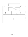
- the DMOS product includes a substrate 1, a dielectric 2, a metal 3, and a passivation layer 4.
- the passivation layer 4 is a silicon nitride layer with a thickness about 10000 angstroms.
- a high voltage DMOS product is required to undergo a HTRB (High Temperature Reverse Bias) test and HTGB (High Temperature Gate Bias) test.
- the DMOS product needs to meet different requirements according to different applications. Some low-end products merely need to pass a 168 hours test, but some high-end products are required to pass a 1000 hours test. It can be found that in actual production, when many products undergo a test of more than 500 hours, a large amount of aluminum is corroded after the product being soaked in a hydrochloric acid (i.e. pinhole test), and the passivation layer 4 has cracks thereon, such that an electric leakage can easily occurs.
- a hydrochloric acid i.e. pinhole test
- the present invention provides a new method of forming a passivation layer of a MOS device and a MOS device, to alleviate the cracking problem.
- the present invention provides a method of forming a passivation layer of a MOS device, the method includes:
- a thickness of the TEOS is in a range from 9000 to 11000 angstroms
- a thickness of the PSG is in a range from 2700 to 3300 angstroms
- the nitrogen silicon compound can be SiON
- a thickness of the SiON is in a range from 2700 to 3300 angstroms
- the nitrogen silicon compound can also be SiN.
- the thickness of the TEOS is 10000 angstroms
- the thickness of the PSG is 3000 angstroms
- the thickness of the SiON is 3000 angstroms.
- the TEOS, the PSG, the SiON or the TEOS, the PSG, the SiN are formed by a chemical vapor deposition method.
- the MOS device is a CMOS device or a DMOS device.
- the present invention further provides a MOS device, the MOS device includes:
- a thickness of the TEOS is in a range from 9000 to 11000 angstroms
- a thickness of the PSG is in a range from 2700 to 3300 angstroms
- the nitrogen silicon compound can be SiON
- a thickness of the SiON is in a range from 2700 to 3300 angstroms
- the nitrogen silicon compound also can be SiN.
- the thickness of the TEOS is 10000 angstroms
- the thickness of the PSG is 3000 angstroms
- the thickness of the SiON is 3000 angstroms.
- the TEOS, the PSG, the SiON or the TEOS, the PSG, the SiN are formed by a chemical vapor deposition method.
- the MOS device is a CMOS device or a DMOS device.
- TEOS and the PSG on the bottom can efficiently relief a stress of the top layers, and at the same time, a stress of the nitrogen silicon compound is relative less than that of original, thereby efficiently improving the cracks problems of the passivation layer.
- a condemnation factor of the product can be efficiently reduced, thereby enhancing a generating efficiency thereof.
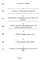
- FIG. 2 is a flow chart of a method of forming a passivation layer of a MOS device a according to an exemplary embodiment of the present invention. As shown in the figure, the method includes steps as follows:
- the substrate can be a mono-crystalline silicon with a crystal orientation of ⁇ 100> and a resistance of 15 ⁇ 25 ohms.
- the dielectric can be oxide layer, for example, an oxide silicon layer.
- the dielectric is patterned to expose a part of the substrate.
- a metal is formed on the exposed part of the substrate, and the dielectric.
- the metal can be aluminum, for example.
- a TEOS tetraethyl orthosilicate
- the thickness of the TEOS is 9000 to 11000 angstroms, and more preferably, the thickness of the TEOS is 10000 angstroms.
- a PSG phosphosilicate glass
- the thickness of the PSG is 2700 to 3300 angstroms, and more preferably, the thickness of the PSG is 3000 angstroms.
- a nitrogen silicon compound is formed on the PSG.
- the thickness of the nitrogen silicon compound (SiON) is 2700 to 3300 angstroms, and more preferably, the thickness of the nitrogen silicon compound (SiON) is 3000 angstroms.
- the SiON can be substituted by SiN.
- the TEOS, the PSG, and the SiON are formed by a chemical vapor deposition method.
- MOS device is a CMOS (Complementary Metal Oxide Semiconductor) device or a DMOS device.
- CMOS Complementary Metal Oxide Semiconductor
- FIG. 3 is a schematic view of structure of the MOS device according to an embodiment of the present invention.
- the nitrogen silicon compound in the process of forming the passivation layer can be SiON or SiN and so on.
- SiON is illustrated as a nitrogen silicon compound in the following embodiment for example, as shown in the figure, the MOS device includes a substrate 1, a dielectric 2 formed on a part of the substrate 1, a metal 3 formed on the substrate 1 and the dielectric 2, and a passivation layer 4' formed on the metal 3.
- the passivation layer 4' includes:
- the thickness of the TEOS 41 is 9000 to 11000 angstroms
- the thickness of the PSG 42 is 2700 to 3300 angstroms
- the thickness of the SiON 43 is 2700 to 3000 angstroms.
- the thickness of the TEOS 41 is 10000 angstroms
- the thickness of the PSG 42 is 3000 angstroms
- the thickness of the SiON 43 is 3000 angstroms.
- the TEOS 41, the PSG 42, and the SiON 43 are formed by a chemical vapor deposition method.
- MOS device is a CMOS device or a DMOS device.
Landscapes
- Formation Of Insulating Films (AREA)
- Chemical & Material Sciences (AREA)
- Engineering & Computer Science (AREA)
- Ceramic Engineering (AREA)
- Chemical Kinetics & Catalysis (AREA)
Abstract
Description
- The present invention relates to a field of semiconductor device manufacturing, and more particularly, relates to a method of forming a passivation layer of a MOS (Metal Oxide Semiconductor) device, and a MOS device.
- As shown in
FIG. 1 , structure of a prior art DMOS (Double-diffusion Metal Oxide Semiconductor) product are shown. The DMOS product includes asubstrate 1, a dielectric 2, ametal 3, and apassivation layer 4. Wherein, thepassivation layer 4 is a silicon nitride layer with a thickness about 10000 angstroms. - Generally, a high voltage DMOS product is required to undergo a HTRB (High Temperature Reverse Bias) test and HTGB (High Temperature Gate Bias) test. The DMOS product needs to meet different requirements according to different applications. Some low-end products merely need to pass a 168 hours test, but some high-end products are required to pass a 1000 hours test. It can be found that in actual production, when many products undergo a test of more than 500 hours, a large amount of aluminum is corroded after the product being soaked in a hydrochloric acid (i.e. pinhole test), and the
passivation layer 4 has cracks thereon, such that an electric leakage can easily occurs. - In view of this, the present invention provides a new method of forming a passivation layer of a MOS device and a MOS device, to alleviate the cracking problem.
- The present invention provides a method of forming a passivation layer of a MOS device, the method includes:
- forming a substrate;
- forming a dielectric on the substrate;
- patterning the dielectric to expose a part of the substrate;
- forming a metal on the exposed part of the substrate, and the dielectric;
- forming a TEOS on the metal;
- forming a PSG on the TEOS; and
- forming a nitrogen silicon compound on the PSG.
- Preferably, in above-described method of the present invention, a thickness of the TEOS is in a range from 9000 to 11000 angstroms, a thickness of the PSG is in a range from 2700 to 3300 angstroms, the nitrogen silicon compound can be SiON, and a thickness of the SiON is in a range from 2700 to 3300 angstroms, additionally, the nitrogen silicon compound can also be SiN.
- Preferably, in above-described method of the present invention, the thickness of the TEOS is 10000 angstroms, the thickness of the PSG is 3000 angstroms, and the thickness of the SiON is 3000 angstroms.
- Preferably, in above-described method of the present invention, the TEOS, the PSG, the SiON or the TEOS, the PSG, the SiN are formed by a chemical vapor deposition method.
- Preferably, in above-described method of the present invention, the MOS device is a CMOS device or a DMOS device.
- The present invention further provides a MOS device, the MOS device includes:
- a substrate;
- a dielectric formed on a part of the substrate;
- a metal formed on the substrate and the dielectric; and
- a passivation layer formed on the metal, including:
- a TEOS formed on the metal;
- a PSG formed on the TEOS; and
- a nitrogen silicon compound formed on the PSG.
- Preferably, in above-described MOS device of the present invention, a thickness of the TEOS is in a range from 9000 to 11000 angstroms, a thickness of the PSG is in a range from 2700 to 3300 angstroms, the nitrogen silicon compound can be SiON, and a thickness of the SiON is in a range from 2700 to 3300 angstroms, the nitrogen silicon compound also can be SiN.
- Preferably, in above-described MOS device of the present invention, the thickness of the TEOS is 10000 angstroms, the thickness of the PSG is 3000 angstroms, and the thickness of the SiON is 3000 angstroms.
- Preferably, in above-described MOS device of the present invention, the TEOS, the PSG, the SiON or the TEOS, the PSG, the SiN are formed by a chemical vapor deposition method.
- Preferably, in above-described MOS device of the present invention, the MOS device is a CMOS device or a DMOS device.
- In the present invention, as the TEOS and the PSG on the bottom can efficiently relief a stress of the top layers, and at the same time, a stress of the nitrogen silicon compound is relative less than that of original, thereby efficiently improving the cracks problems of the passivation layer.
- In the present invention, a condemnation factor of the product can be efficiently reduced, thereby enhancing a generating efficiency thereof.
-
-
FIG. 1 is a schematic view of structure of a DMOS product in accordance with prior art; -
FIG. 2 is a flow chart of a method for forming of a MOS device passivation layer according to an exemplary embodiment of the present invention; and -
FIG. 3 is a schematic view of structure of the MOS device according to an exemplary embodiment of the present invention. - The following clearly describes the preferred embodiments of the present invention with reference to the accompanying drawings. The use of the same reference numbers in different instances in the figures indicate identical elements.
-
FIG. 2 is a flow chart of a method of forming a passivation layer of a MOS device a according to an exemplary embodiment of the present invention. As shown in the figure, the method includes steps as follows: - S1, a substrate is formed. The substrate can be a mono-crystalline silicon with a crystal orientation of <100> and a resistance of 15∼25 ohms.
- S2, a dielectric is formed on the substrate. The dielectric can be oxide layer, for example, an oxide silicon layer.
- S3, the dielectric is patterned to expose a part of the substrate.
- S4, a metal is formed on the exposed part of the substrate, and the dielectric. The metal can be aluminum, for example.
- S5, a TEOS (tetraethyl orthosilicate) is formed on the metal. Preferably, the thickness of the TEOS is 9000 to 11000 angstroms, and more preferably, the thickness of the TEOS is 10000 angstroms.
- S6, a PSG (phosphosilicate glass) is formed on the TEOS. Preferably, the thickness of the PSG is 2700 to 3300 angstroms, and more preferably, the thickness of the PSG is 3000 angstroms.
- S7, a nitrogen silicon compound is formed on the PSG. Preferably, the thickness of the nitrogen silicon compound (SiON) is 2700 to 3300 angstroms, and more preferably, the thickness of the nitrogen silicon compound (SiON) is 3000 angstroms. In addition, the SiON can be substituted by SiN.
- Preferably, the TEOS, the PSG, and the SiON are formed by a chemical vapor deposition method.
- Preferably, above-described MOS device is a CMOS (Complementary Metal Oxide Semiconductor) device or a DMOS device.
-
FIG. 3 is a schematic view of structure of the MOS device according to an embodiment of the present invention. The nitrogen silicon compound in the process of forming the passivation layer can be SiON or SiN and so on. SiON is illustrated as a nitrogen silicon compound in the following embodiment for example, as shown in the figure, the MOS device includes asubstrate 1, a dielectric 2 formed on a part of thesubstrate 1, ametal 3 formed on thesubstrate 1 and the dielectric 2, and a passivation layer 4' formed on themetal 3. The passivation layer 4' includes: - a
TEOS 41 formed on themetal 3; - a
PSG 42 formed on theTEOS 41; and - a
SiON 43 formed on thePSG 42. - Preferably, the thickness of the
TEOS 41 is 9000 to 11000 angstroms, the thickness of thePSG 42 is 2700 to 3300 angstroms, and the thickness of theSiON 43 is 2700 to 3000 angstroms. - More preferably, the thickness of the
TEOS 41 is 10000 angstroms, the thickness of thePSG 42 is 3000 angstroms, and the thickness of theSiON 43 is 3000 angstroms. - Preferably, the
TEOS 41, thePSG 42, and theSiON 43 are formed by a chemical vapor deposition method. - Preferably, above-described MOS device is a CMOS device or a DMOS device.
- In view of these teachings, a technical person skilled in the art can readily envisage of other embodiments of the present invention, combinations and modifications. Accordingly, when reading combined with the foregoing description and accompanying drawings, the present invention is only defined by the claims.
Claims (10)
- A method of forming a passivation layer of a MOS device, comprising:forming a substrate;forming a dielectric on the substrate;patterning the dielectric to expose a part of the substrate;forming a metal on the exposed part of the substrate, and the dielectric;forming a TEOS on the metal;forming a PSG on the TEOS; andforming a nitrogen silicon compound on the PSG.
- The method according to claim 1, wherein a thickness of the TEOS is in a range of from 9000 to 11000 angstroms, a thickness of the PSG is in a range from 2700 to 3300 angstroms, the nitrogen silicon compound can be SiON, and a thickness of the SiON is in a range from 2700 to 3300 angstroms, additionally, the nitrogen silicon compound also can be SiN.
- The method according to claim 2, wherein the thickness of the TEOS is 10000 angstroms, the thickness of the PSG is 3000 angstroms, and the thickness of the SION is 3000 angstroms.
- The method according to claim 2, wherein the TEOS, the PSG, the SiON or the TEOS, the PSG, the SiN are formed by a chemical vapor deposition method.
- The method according to claim 1, wherein the MOS device is a CMOS device or a DMOS device.
- AMOS device, comprising:a substrate;a dielectric formed on a part of the substrate;a metal formed on the substrate and the dielectric; anda passivation layer formed on the metal, comprising:a TEOS formed on the metal;a PSG formed on the TEOS; anda nitrogen silicon compound formed on the PSG.
- The MOS device according to claim 6, wherein a thickness of the TEOS is in a range from 9000 to 11000 angstroms, a thickness of the PSG is in a range from 2700 to 3300 angstroms, the nitrogen silicon compound can be SiON, and a thickness of the SiON is in a range from 2700 to 3300 angstroms, additionally, the nitrogen silicon compound can also be SiN.
- The MOS device according to claim 7, wherein the thickness of the TEOS is 10000 angstroms, the thickness of the PSG is 3000 angstroms, and the thickness of the SION is 3000 angstroms.
- The MOS device according to claim 7, wherein the TEOS, the PSG, the SiON or the TEOS, the PSG, the SiN are formed by a chemical vapor deposition method.
- The MOS device according to claim 6, wherein the MOS device is a CMOS device or a DMOS device.
Applications Claiming Priority (2)
| Application Number | Priority Date | Filing Date | Title |
|---|---|---|---|
| CN201210260811.6A CN103578919A (en) | 2012-07-26 | 2012-07-26 | Method for forming passivation layer of MOS device and MOS device |
| PCT/CN2013/080149 WO2014015820A1 (en) | 2012-07-26 | 2013-07-25 | Method for forming mos device passivation layer and mos device |
Publications (2)
| Publication Number | Publication Date |
|---|---|
| EP2879172A1 true EP2879172A1 (en) | 2015-06-03 |
| EP2879172A4 EP2879172A4 (en) | 2016-03-02 |
Family
ID=49996610
Family Applications (1)
| Application Number | Title | Priority Date | Filing Date |
|---|---|---|---|
| EP13822224.5A Withdrawn EP2879172A4 (en) | 2012-07-26 | 2013-07-25 | METHOD FOR FORMING MOS DEVICE PASSIVATION LAYER AND MOS DEVICE |
Country Status (4)
| Country | Link |
|---|---|
| US (1) | US9559032B2 (en) |
| EP (1) | EP2879172A4 (en) |
| CN (1) | CN103578919A (en) |
| WO (1) | WO2014015820A1 (en) |
Families Citing this family (1)
| Publication number | Priority date | Publication date | Assignee | Title |
|---|---|---|---|---|
| CN113436959A (en) * | 2021-01-26 | 2021-09-24 | 德兴市意发功率半导体有限公司 | Composite passivation film and manufacturing method thereof |
Family Cites Families (23)
| Publication number | Priority date | Publication date | Assignee | Title |
|---|---|---|---|---|
| JPH0370178A (en) * | 1989-08-09 | 1991-03-26 | Seiko Instr Inc | Semiconductor device |
| JP3131982B2 (en) * | 1990-08-21 | 2001-02-05 | セイコーエプソン株式会社 | Semiconductor device, semiconductor memory, and method of manufacturing semiconductor device |
| US5650359A (en) * | 1991-05-06 | 1997-07-22 | Texas Instruments Incorporated | Composite dielectric passivation of high density circuits |
| JP3144579B2 (en) * | 1991-12-02 | 2001-03-12 | 株式会社日立製作所 | Semiconductor integrated circuit device |
| US5334554A (en) * | 1992-01-24 | 1994-08-02 | Taiwan Semiconductor Manufacturing Co., Ltd. | Nitrogen plasma treatment to prevent field device leakage in VLSI processing |
| KR0128491B1 (en) * | 1993-04-14 | 1998-04-07 | 모리시다 요이치 | Semiconductor device and manufacturing method thereof |
| EP0627763B1 (en) * | 1993-05-31 | 2004-12-15 | STMicroelectronics S.r.l. | Process for improving the adhesion between dielectric layers at their interface in semiconductor devices manufacture |
| US6127261A (en) * | 1995-11-16 | 2000-10-03 | Advanced Micro Devices, Inc. | Method of fabricating an integrated circuit including a tri-layer pre-metal interlayer dielectric compatible with advanced CMOS technologies |
| US6025279A (en) * | 1998-05-29 | 2000-02-15 | Taiwan Semiconductor Manufacturing Company | Method of reducing nitride and oxide peeling after planarization using an anneal |
| US6087726A (en) * | 1999-03-01 | 2000-07-11 | Lsi Logic Corporation | Metal interconnect stack for integrated circuit structure |
| US6300252B1 (en) * | 1999-10-01 | 2001-10-09 | Taiwan Semiconductor Manufacturing Company, Ltd | Method for etching fuse windows in IC devices and devices made |
| KR100362189B1 (en) * | 1999-12-30 | 2002-11-23 | 주식회사 하이닉스반도체 | Semiconductor memory device having oxide and Ti double layer capable of preventing hydrogen diffusion and method for forming the same |
| US6498088B1 (en) * | 2000-11-09 | 2002-12-24 | Micron Technology, Inc. | Stacked local interconnect structure and method of fabricating same |
| US6709930B2 (en) * | 2002-06-21 | 2004-03-23 | Siliconix Incorporated | Thicker oxide formation at the trench bottom by selective oxide deposition |
| TW559950B (en) * | 2002-03-13 | 2003-11-01 | Macronix Int Co Ltd | Memory device and method of forming passivation film thereof |
| US7109119B2 (en) * | 2002-10-31 | 2006-09-19 | Taiwan Semiconductor Manufacturing Company, Ltd. | Scum solution for chemically amplified resist patterning in cu/low k dual damascene |
| US20060081965A1 (en) * | 2004-10-15 | 2006-04-20 | Ju-Ai Ruan | Plasma treatment of an etch stop layer |
| JP5448304B2 (en) * | 2007-04-19 | 2014-03-19 | パナソニック株式会社 | Semiconductor device |
| CN100576461C (en) * | 2007-06-21 | 2009-12-30 | 中芯国际集成电路制造(上海)有限公司 | Benzocyclobutene layer deposition method and bump manufacturing method |
| KR20090044262A (en) * | 2007-10-31 | 2009-05-07 | 주식회사 동부하이텍 | Semiconductor device and its manufacturing method |
| US9076798B2 (en) * | 2009-05-11 | 2015-07-07 | Taiwan Semiconductor Manufacturing Company, Ltd. | Dicing structures for semiconductor substrates and methods of fabrication thereof |
| US8432038B2 (en) * | 2009-06-12 | 2013-04-30 | Taiwan Semiconductor Manufacturing Company, Ltd. | Through-silicon via structure and a process for forming the same |
| CN101710580B (en) * | 2009-12-01 | 2011-12-14 | 杭州士兰集成电路有限公司 | Multi-layer compound passivation layer structure of Bipolar circuit and manufacturing process thereof |
-
2012
- 2012-07-26 CN CN201210260811.6A patent/CN103578919A/en active Pending
-
2013
- 2013-07-25 WO PCT/CN2013/080149 patent/WO2014015820A1/en not_active Ceased
- 2013-07-25 EP EP13822224.5A patent/EP2879172A4/en not_active Withdrawn
- 2013-07-25 US US14/412,445 patent/US9559032B2/en active Active
Also Published As
| Publication number | Publication date |
|---|---|
| CN103578919A (en) | 2014-02-12 |
| EP2879172A4 (en) | 2016-03-02 |
| WO2014015820A1 (en) | 2014-01-30 |
| US9559032B2 (en) | 2017-01-31 |
| US20150364397A1 (en) | 2015-12-17 |
Similar Documents
| Publication | Publication Date | Title |
|---|---|---|
| US8772151B2 (en) | Passivation scheme | |
| US9508755B2 (en) | Pixel unit and method of fabricating the same, array substrate and display device | |
| US11411203B2 (en) | Barrier film, organic el device, flexible substrate, and method for manufacturing barrier film | |
| JP2012160748A5 (en) | ||
| CN102522388B (en) | Inductance and formation method | |
| EP4141934B1 (en) | Array substrate and fabricating method therefor, and display device | |
| US20160133689A1 (en) | Reliability improvement of polymer-based capacitors by moisture barrier | |
| US20110180922A1 (en) | Semiconductor chip, seal-ring structure and manufacturing process thereof | |
| US10082714B2 (en) | Thin-film transistor substrate manufacturing method, thin-film transistor substrate, and liquid crystal panel | |
| EP2879172A1 (en) | Method for forming mos device passivation layer and mos device | |
| TWI485777B (en) | Integrated circuit and its method | |
| CN105655367B (en) | Improved high performance fluxgate device | |
| CN1992226A (en) | Method for fabricating an integrated circuit on a semiconductor substrate | |
| US20150249010A1 (en) | Semiconductor device and method of manufacturing same | |
| US7781775B2 (en) | Production method of semiconductor device and semiconductor device | |
| CN104752514B (en) | A kind of thin film transistor (TFT) and its preparation method and application | |
| CN108475724A (en) | Integrated Fluxgate Device | |
| JP6583014B2 (en) | Manufacturing method of semiconductor device | |
| US9006702B2 (en) | Semiconductor structure including a zirconium oxide material | |
| TWI430399B (en) | Method of making multi-layer structure for metal-insulator-metal capacitor | |
| JP6871190B2 (en) | Semiconductor devices and methods for manufacturing semiconductor devices | |
| JP2011077294A (en) | Method of manufacturing semiconductor device | |
| JP2010165778A (en) | Method of manufacturing semiconductor device | |
| CN104300000A (en) | Power device with electrostatic protection structure and manufacturing method thereof | |
| CN102930981B (en) | A kind of electric capacity and preparation method thereof |
Legal Events
| Date | Code | Title | Description |
|---|---|---|---|
| PUAI | Public reference made under article 153(3) epc to a published international application that has entered the european phase |
Free format text: ORIGINAL CODE: 0009012 |
|
| 17P | Request for examination filed |
Effective date: 20141224 |
|
| AK | Designated contracting states |
Kind code of ref document: A1 Designated state(s): AL AT BE BG CH CY CZ DE DK EE ES FI FR GB GR HR HU IE IS IT LI LT LU LV MC MK MT NL NO PL PT RO RS SE SI SK SM TR |
|
| AX | Request for extension of the european patent |
Extension state: BA ME |
|
| DAX | Request for extension of the european patent (deleted) | ||
| RA4 | Supplementary search report drawn up and despatched (corrected) |
Effective date: 20160201 |
|
| RIC1 | Information provided on ipc code assigned before grant |
Ipc: H01L 21/02 20060101ALI20160126BHEP Ipc: H01L 23/31 20060101ALI20160126BHEP Ipc: H01L 21/00 20060101ALI20160126BHEP Ipc: H01L 23/535 20060101ALI20160126BHEP Ipc: H01L 23/00 20060101ALI20160126BHEP Ipc: H01L 21/768 20060101AFI20160126BHEP |
|
| STAA | Information on the status of an ep patent application or granted ep patent |
Free format text: STATUS: EXAMINATION IS IN PROGRESS |
|
| 17Q | First examination report despatched |
Effective date: 20180614 |
|
| STAA | Information on the status of an ep patent application or granted ep patent |
Free format text: STATUS: THE APPLICATION IS DEEMED TO BE WITHDRAWN |
|
| 18D | Application deemed to be withdrawn |
Effective date: 20200902 |