EP2877957B2 - Verfahren und vorrichtung zum schutz vor fehlerangriffen in einem elektronischen gerät mit cache-speicher - Google Patents
Verfahren und vorrichtung zum schutz vor fehlerangriffen in einem elektronischen gerät mit cache-speicher Download PDFInfo
- Publication number
- EP2877957B2 EP2877957B2 EP13739694.1A EP13739694A EP2877957B2 EP 2877957 B2 EP2877957 B2 EP 2877957B2 EP 13739694 A EP13739694 A EP 13739694A EP 2877957 B2 EP2877957 B2 EP 2877957B2
- Authority
- EP
- European Patent Office
- Prior art keywords
- value
- cache memory
- redundancy
- electronic device
- memory
- Prior art date
- Legal status (The legal status is an assumption and is not a legal conclusion. Google has not performed a legal analysis and makes no representation as to the accuracy of the status listed.)
- Active
Links
Images
Classifications
-
- G—PHYSICS
- G06—COMPUTING OR CALCULATING; COUNTING
- G06F—ELECTRIC DIGITAL DATA PROCESSING
- G06F21/00—Security arrangements for protecting computers, components thereof, programs or data against unauthorised activity
- G06F21/70—Protecting specific internal or peripheral components, in which the protection of a component leads to protection of the entire computer
- G06F21/71—Protecting specific internal or peripheral components, in which the protection of a component leads to protection of the entire computer to assure secure computing or processing of information
- G06F21/77—Protecting specific internal or peripheral components, in which the protection of a component leads to protection of the entire computer to assure secure computing or processing of information in smart cards
-
- G—PHYSICS
- G06—COMPUTING OR CALCULATING; COUNTING
- G06F—ELECTRIC DIGITAL DATA PROCESSING
- G06F21/00—Security arrangements for protecting computers, components thereof, programs or data against unauthorised activity
- G06F21/70—Protecting specific internal or peripheral components, in which the protection of a component leads to protection of the entire computer
- G06F21/71—Protecting specific internal or peripheral components, in which the protection of a component leads to protection of the entire computer to assure secure computing or processing of information
- G06F21/75—Protecting specific internal or peripheral components, in which the protection of a component leads to protection of the entire computer to assure secure computing or processing of information by inhibiting the analysis of circuitry or operation
- G06F21/755—Protecting specific internal or peripheral components, in which the protection of a component leads to protection of the entire computer to assure secure computing or processing of information by inhibiting the analysis of circuitry or operation with measures against power attack
-
- G—PHYSICS
- G06—COMPUTING OR CALCULATING; COUNTING
- G06F—ELECTRIC DIGITAL DATA PROCESSING
- G06F21/00—Security arrangements for protecting computers, components thereof, programs or data against unauthorised activity
- G06F21/70—Protecting specific internal or peripheral components, in which the protection of a component leads to protection of the entire computer
- G06F21/78—Protecting specific internal or peripheral components, in which the protection of a component leads to protection of the entire computer to assure secure storage of data
- G06F21/79—Protecting specific internal or peripheral components, in which the protection of a component leads to protection of the entire computer to assure secure storage of data in semiconductor storage media, e.g. directly-addressable memories
-
- H—ELECTRICITY
- H04—ELECTRIC COMMUNICATION TECHNIQUE
- H04L—TRANSMISSION OF DIGITAL INFORMATION, e.g. TELEGRAPHIC COMMUNICATION
- H04L9/00—Cryptographic mechanisms or cryptographic arrangements for secret or secure communications; Network security protocols
- H04L9/002—Countermeasures against attacks on cryptographic mechanisms
- H04L9/004—Countermeasures against attacks on cryptographic mechanisms for fault attacks
Definitions
- the present invention relates to devices or products comprising hardware and software capable of executing a sensitive process using a cache memory, and needing to be resistant to fault attacks.
- a fault attack is a type of physical attack that consists in submitting a device to unusual environmental conditions to modify the execution of a sensitive process (for instance by introducing a value discrepancy) and then deduce sensitive information from its alter behaviour or results and/or to modify the attacked sensitive process.
- the aim of a fault attack may be determination of a secret or a ciphering/deciphering or cryptographic key or modification of a value to get additional rights (such as access or credits).
- code redundancy may consist in reading a value, that is stored into a memory of an electronic device at different instants separated by a chosen time interval, and then in considering that this electronic device has been subject to a fault attack when these read values differ therebetween.
- an objective of the invention is to improve fault attack detections into electronic devices comprising hardware and software capable of executing a sensitive process using a cache memory.
- the invention provides a method for protecting against fault attack(s) an electronic device comprising hardware and software capable of executing a sensitive process using a cache memory and implementing redundancy checks, said method comprising at least a step (i) during which said cache memory is filled with a first value originating from an external memory, a step (ii) during which said first value is read into said cache memory and a step (iii) implementing at least a redundancy check, characterized in that it further comprises a fundamental step to guarantee that any redundant reading inside the redundancy check will extract a value from cache memory which is numerically equal to the genuine value in the external memory.
- the fundamental step of the invention implies that none redundancy check is processed if a risk exists that the value stored in the cache memory is wrong. It enables to insure that redundancy checks are not based on a corrupted value. This increases the efficiency of the fault attack detection by eliminating the risk to make redundancy checks based on a wrong value as it previously occurs.
- the method implementing hardware integrity checks wherein the value stored in the cache memory is compared with the value stored into the external memory, the fundamental step introduces, between a reading and its redundancy, a delay of a chosen duration longer than the duration between two integrity checks.
- the invention consists in waiting a next integrity check of the sensitive code before introducing a redundancy. It ensures that an integrity check is always performed by the hardware before the execution of the redundancy.
- the integrity check fails and thus if a corruption of the value in cache memory is detected, a security action is triggered. If the integrity check does not fail, a redundancy check is further performed by software.
- the value in cache memory is read for redundancy check, to detect if the electronic device is subject to a fault attack.
- Redundancy check may be periodically or randomly implemented.
- the invention also provides a protection device, intended for equipping an electronic device comprising hardware and software capable of executing a sensitive process using a cache memory, and arranged for implementing redundancy checks, for filing said cache memory with a first value originating from an external memory, for reading said first value into said cache memory, characterized in that it is arranged for guaranteeing that any redundant reading inside the redundancy check will extract a value from cache memory which is numerically equal to the genuine value in the external memory.
- the protection device is arranged for implementing hardware integrity checks, wherein the integrity of the value stored in the cache memory is checked, for introducing, between a reading and its redundancy, a delay of a chosen duration longer than the duration between two integrity checks.
- the invention also provides an electronic device comprising hardware and software capable of executing a sensitive process using a cache memory and a control device such as the one above introduced.
- This electronic device may be chosen from a group comprising at least a smart card, a memory card reader, a communication device, and a portable memory means.
- the invention aims, notably, at offering a protection method, and an associated protection device PD, intended for protecting an electronic device ED from fault attack(s) of attacker(s).
- the invention concerns any electronic device ED comprising hardware and software capable of executing a sensitive process SP using a cache memory CM, notably for security redundancy.
- the electronic device ED is a smart card.
- it may be a credit card or an electronic identity card or else an electronic passport.
- the invention is not limited to this type of electronic device. It concerns a lot of secured devices, and notably memory card readers, communication devices (for instance smart phones or electronic tablets or else Set-Top Boxes, Machine To Machine), and portable memory means (for instance USB keys).
- the sensitive process may be an electronic transaction or an user / mutual authentication or else an exchange of secret data (obtained by means of a ciphering or cryptographic algorithm).
- the electronic device ED comprises a microprocessor (or microcontroller) MP, which comprises hardware and software capable of executing a sensitive process SP using a cache memory CM, and a protection device PD according to the invention coupled to this sensitive process SP in order to protect it against fault attack(s) of attacker(s).
- a microprocessor or microcontroller
- MP microprocessor
- CM cache memory
- PD protection device
- the protection device PD is not mandatorily located into the microprocessor MP (or any equivalent means, such as integrated circuits, for instance). Indeed, it may be a device that is coupled to the microprocessor MP and may access to the sensitive process SP that is running in it. Such a device PD may be also located into another device of the electronic device ED.
- a protection device PD can be made of software modules, at least partly, or of electronic circuit(s) or hardware modules, or else of a combination of hardware and software modules.
- it can be stored in a memory means or in any computer software product which can be read by an electronic device.
- the invention proposes a protection method based on redundancy checks and comprising three main steps (i), (ii) and (iii).
- Such a method may be implemented, at least partly, by a protection device PD associated to an electronic device ED. Moreover, such a method may be periodically or randomly implemented, for instance.
- a first step (i) of this protection method comprises a phase during which the cache memory CM of the electronic device ED is filled at a chosen address with a first value V1 originating from an external memory EM.
- This first filling may be carried out by the sensitive process running into the microprocessor MP of the electronic device ED or by the protection device D.
- This first value V1 is supposed to be a copy of a variable value V0 that is stored into the external memory EM.
- Such a variable value may be, for instance, representative of an action, such as a PIN verification, or of a status, or of the current value of a counter, or of a transaction amount, or else a part of a secret key.
- this first step (i) may be preceded by a preliminary step or may comprise a preliminary phase during which the external memory EM is filled with the variable value V0.
- the external memory EM is defined into the microprocessor MP. But this is not mandatory. Indeed, the external memory EM could be located into another electronic device capable of establishing communications with the electronic device ED.
- the electronic device ED may be subject to a fault attack intended to introduce a discrepancy by replacing the variable value V0 (stored into the external memory EM and to be stored into the cache memory CM) with a faulty value.
- a second step (ii) of the protection method comprises a phase during which the first value is read into the chosen address of the cache memory CM by the protection device D.
- a third step (iii) of the protection method is a redundancy test. It is such that it further comprises a fundamental step to guarantee that any redundant reading inside the redundancy check will extract a value from cache memory which is numerically equal to the genuine value in the external memory.
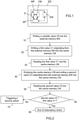
- a first one of these embodiments is comprised in the first example of algorithm illustrated in figure 2 . This first embodiment described below is excluded from the scope of the invention.
- this first algorithm starts with a sub step 10 during which the external memory EM is filled with a variable value V0 representative of an action.
- the first step (i) of the protection method comprises the sub step 20 and possibly the sub step 10.
- the first algorithm comprises a sub step 30 during which the first value V1 is read into the dedicated address of the cache memory CM.
- the second step (ii) of the protection method comprises this sub step 30.
- the reading of the value V1 may serve in a calculation that will be redundantly performed later.
- the first algorithm comprises a sub step 40 during which the cache memory CM is emptied (or voided) at the above mentioned dedicated address, and then this cache memory CM is filled again into the same dedicated address with a second value V2 originating from the external memory EM (and supposed to be the variable value V0).
- the first value V1 stored in cache memory is systematically regarded as different from the value V0 stored into the external memory EM. It is thus deleted.
- the cache memory CM is systematically emptied (or voided) after the first value V1 has been read into the cache memory CM. This implies a new filling of the cache memory with a value read in the external memory and thus corrected if ever the first copying was attacked. The redundant reading will thus extract a genuine value from the cache memory.
- the first value V1 could be first compared with the variable value V0, preferably through hardware operations.
- the first algorithm comprises a sub step 50 during which the second value V2 is read into the dedicated address of the cache memory CM.
- the first algorithm may follow with a sub step 60 during which the second value V2 is compared with the first value V1 or a redundant calculation is performed using the value V2 stored in the cache memory CM and the result is compared to a same previously performed calculation.
- the first algorithm comprises a sub step 70 during which a security action is triggered because it is considered that the electronic device ED has been subject to a fault attack. So no other sensitive action may be carried out with the electronic device ED.
- the first algorithm comprises a sub step 80 during which the redundancy check (and therefore the protection method) comes to an end because it is considered that the electronic device ED has not yet been subject to a fault attack. So other sensitive actions, such as a transaction or an user authentication, may be possibly carried out with the electronic device ED.
- the third step (iii) of the protection method comprises the sub steps 40 to 80.
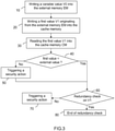
- a second embodiment is comprised in the second example of algorithm illustrated in figure 3 .
- This second embodiment is in accordance with the invention.
- this second algorithm starts with a sub step 10 during which the external memory EM is filled with a variable value V0 representative of an action.
- a sub step 20 during which a first value V1 originating from the external memory EM (and supposed to be the variable value V0) is written into a dedicated address of the cache memory CM of the electronic device ED.
- the first step (i) of the protection method comprises the sub step 20 and possibly the sub step 10.
- the second algorithm comprises a sub step 30 during which the first value V1 is read into the dedicated address of the cache memory CM.
- the second step (ii) of the protection method comprises this sub step 30.
- the second algorithm comprises a sub step 40 during which the integrity of the first value V1 is checked.
- This check is like and indirect comparison with the variable value V0 (stored into the external memory EM).
- the second algorithm may follow with a sub step 50 during which a security action is triggered because it is considered that the electronic device ED has been subject to a fault attack.
- the second algorithm may follow with a sub step 60 where a redundancy check is performed using the value V1 stored in the cache memory CM.
- the redundancy check is thus classically performed through a comparison with the value previously read in the cache memory CM or through a comparison of the result of a redundant calculation using the value read in cache memory CM.
- the second algorithm comprises a sub step 70 during which a security action is triggered because it is considered that the electronic device ED has been subject to a fault attack. So no other sensitive action may be carried out with the electronic device ED.
- the second algorithm comprises a sub step 80 during which the cache check (and therefore the protection method) comes to an end because it is considered that the electronic device ED has not yet been subject to a fault attack. So other sensitive actions, such as a transaction or an user authentication, may be possibly carried out with the electronic device ED.
- the third step (iii) of the protection method comprises the sub steps 40 to 80.
- the invention offers a low cost solution to by-pass a hardware cache mechanism that induces incontrollable and weak data manipulation/storage regarding fault attack.
Landscapes
- Engineering & Computer Science (AREA)
- Theoretical Computer Science (AREA)
- Computer Hardware Design (AREA)
- Computer Security & Cryptography (AREA)
- Physics & Mathematics (AREA)
- General Engineering & Computer Science (AREA)
- Software Systems (AREA)
- General Physics & Mathematics (AREA)
- Mathematical Physics (AREA)
- Computer Networks & Wireless Communication (AREA)
- Signal Processing (AREA)
- Memory System Of A Hierarchy Structure (AREA)
- Techniques For Improving Reliability Of Storages (AREA)
Claims (8)
- Verfahren zum Schützen vor (einem) Fehlerangriff(en) einer elektronischen Vorrichtung (ED), umfassend Hardware und Software, die in der Lage ist, einen sensiblen Prozess (SP) unter Verwendung eines Cache-Speichers (CM) auszuführen und Redundanzprüfungen zu implementieren, das Verfahren umfassend mindestens einen Schritt (i), während dessen der Cache-Speicher (CM) mit einem ersten Wert gefüllt wird, der von einem externen Speicher (EM) stammt, einen Schritt (ii), während dessen der erste Wert in den Cache-Speicher (CM) gelesen wird, und einen Schritt (iii), der mindestens eine Redundanzprüfung implementiert, dadurch gekennzeichnet, dass es ferner einen grundlegenden Schritt umfasst, um sicherzustellen, dass ein redundantes Lesen innerhalb der Redundanzprüfung einen Wert aus dem Cache-Speicher (CM) extrahiert, der numerisch dem wahren Wert im externen Speicher (EM) entspricht, wobei der grundlegende Schritt derart ist, dass die Vorrichtung Hardwareintegritätsprüfungen implementiert, wobei die Integrität des im Cache-Speicher gespeicherten Werts überprüft wird, wobei der grundlegende Schritt zwischen einem Lesen und und seiner Redundanz eine Verzögerung einer ausgewählten Dauer, die länger als die Dauer zwischen zwei Integritätsprüfungen ist, einführt.
- Verfahren nach Anspruch 1, dadurch gekennzeichnet, dass, im Fall, dass der erste Wert während der Integritätsprüfung nicht als beschädigt erkannt wird, der Wert im Cache-Speicher (CM) zur Redundanzprüfung gelesen wird.
- Verfahren nach einem der Ansprüche 1 bis 2, dadurch gekennzeichnet, dass, im Fall, dass eine Redundanzprüfung fehlschlägt, eine Sicherheitsaktion ausgelöst wird.
- Verfahren nach einem der Ansprüche 1 bis 3, dadurch gekennzeichnet, dass Redundanzprüfungen periodisch implementiert werden.
- Verfahren nach einem der Ansprüche 1 bis 3, dadurch gekennzeichnet, dass Redundanzprüfungen zufällig implementiert werden.
- Schutzvorrichtung (D) für eine elektronische Vorrichtung (ED), umfassend Hardware und Software, die in der Lage ist, einen sensiblen Prozess (SP) unter Verwendung eines Cache-Speichers (CM) auszuführen, wobei die Schutzvorrichtung (D) zum Implementieren von Redundanzprüfungen, zum Füllen des Cache-Speichers (CM) mit einem ersten Wert, der von einem externen Speicher (EM) stammt, zum Lesen des ersten Werts in den Cache-Speicher (CM) angeordnet ist, dadurch gekennzeichnet, dass sie angeordnet ist, um sicherzustellen, dass ein redundantes Lesen innerhalb der Redundanzprüfung einen Wert aus dem Cache-Speicher (CM) extrahiert, der numerisch dem wahren Wert im externen Speicher (EM) entspricht, wobei die Schutzvorrichtung angeordnet ist zum Implementieren von Hardwareintegritätsprüfungen, wobei die Integrität des im Cache-Speicher gespeicherten Werts überprüft wird, und zum Einführen, zwischen einem Lesen und seiner Redundanz, einer Verzögerung einer ausgewählten Dauer, die länger als die Dauer zwischen zwei Integritätsprüfungen ist.
- Elektronische Vorrichtung (ED), umfassend Hardware und Software, die in der Lage ist, einen sensiblen Prozess (SP) unter Verwendung eines Cache-Speichers (CM) auszuführen, dadurch gekennzeichnet, dass sie ferner eine Schutzvorrichtung (D) nach Anspruch 6 umfasst.
- Elektronische Vorrichtung nach Anspruch 7, dadurch gekennzeichnet, dass sie ausgewählt ist aus einer Gruppe, umfassend mindestens eine Smartcard, einen Speicherkartenleser, eine Kommunikationsvorrichtung und ein tragbares Speichermittel. s
Applications Claiming Priority (2)
| Application Number | Priority Date | Filing Date | Title |
|---|---|---|---|
| EP12305919.8A EP2690579A1 (de) | 2012-07-27 | 2012-07-27 | Verfahren und Vorrichtung zum Schutz vor Fehlerangriffen in einem elektronischen Gerät mit Cache-Speicher |
| PCT/EP2013/065311 WO2014016218A1 (en) | 2012-07-27 | 2013-07-19 | Method and device for protecting against fault attack(s) an electronic device using a cache memory |
Publications (3)
| Publication Number | Publication Date |
|---|---|
| EP2877957A1 EP2877957A1 (de) | 2015-06-03 |
| EP2877957B1 EP2877957B1 (de) | 2019-05-15 |
| EP2877957B2 true EP2877957B2 (de) | 2022-03-09 |
Family
ID=47178531
Family Applications (2)
| Application Number | Title | Priority Date | Filing Date |
|---|---|---|---|
| EP12305919.8A Withdrawn EP2690579A1 (de) | 2012-07-27 | 2012-07-27 | Verfahren und Vorrichtung zum Schutz vor Fehlerangriffen in einem elektronischen Gerät mit Cache-Speicher |
| EP13739694.1A Active EP2877957B2 (de) | 2012-07-27 | 2013-07-19 | Verfahren und vorrichtung zum schutz vor fehlerangriffen in einem elektronischen gerät mit cache-speicher |
Family Applications Before (1)
| Application Number | Title | Priority Date | Filing Date |
|---|---|---|---|
| EP12305919.8A Withdrawn EP2690579A1 (de) | 2012-07-27 | 2012-07-27 | Verfahren und Vorrichtung zum Schutz vor Fehlerangriffen in einem elektronischen Gerät mit Cache-Speicher |
Country Status (2)
| Country | Link |
|---|---|
| EP (2) | EP2690579A1 (de) |
| WO (1) | WO2014016218A1 (de) |
Family Cites Families (5)
| Publication number | Priority date | Publication date | Assignee | Title |
|---|---|---|---|---|
| US6247151B1 (en) * | 1998-06-30 | 2001-06-12 | Intel Corporation | Method and apparatus for verifying that data stored in a memory has not been corrupted |
| JP2001043139A (ja) | 1999-07-29 | 2001-02-16 | Pioneer Electronic Corp | 信号処理装置及びそれに用いる情報記録媒体 |
| KR100476892B1 (ko) * | 2002-04-29 | 2005-03-17 | 삼성전자주식회사 | 데이터의 부정조작을 방지하는 방법 및 그것을 이용한데이터 처리 시스템 |
| JP2009259126A (ja) | 2008-04-18 | 2009-11-05 | Dainippon Printing Co Ltd | 故障攻撃の検知方法、及び、セキュリティデバイス |
| WO2009138892A1 (en) * | 2008-05-15 | 2009-11-19 | Nxp B.V. | A method for secure data reading and a data handling system |
-
2012
- 2012-07-27 EP EP12305919.8A patent/EP2690579A1/de not_active Withdrawn
-
2013
- 2013-07-19 EP EP13739694.1A patent/EP2877957B2/de active Active
- 2013-07-19 WO PCT/EP2013/065311 patent/WO2014016218A1/en not_active Ceased
Also Published As
| Publication number | Publication date |
|---|---|
| EP2690579A1 (de) | 2014-01-29 |
| EP2877957B1 (de) | 2019-05-15 |
| WO2014016218A1 (en) | 2014-01-30 |
| EP2877957A1 (de) | 2015-06-03 |
Similar Documents
| Publication | Publication Date | Title |
|---|---|---|
| CN103679932B (zh) | 一种能读写银行卡的电脑系统 | |
| EP2629447A1 (de) | Verfahren und Vorrichtung zum Schutz einer elektronischen Vorrichtung gegen Fehlerangriff(e) | |
| CN103198347A (zh) | 安全设备防篡改电路 | |
| US20070006224A1 (en) | Controlled execution of a program used for a virtual machine on a portable data carrier | |
| CN102855161A (zh) | 用于安全微控制器的外部存储器的数据交织方案 | |
| Barbu et al. | Java card operand stack: fault attacks, combined attacks and countermeasures | |
| CN111666574A (zh) | 一种bios和主板、硬盘相互绑定的方法 | |
| US10148671B2 (en) | Method for protecting a chip card against a physical attack intended to modify the logical behaviour of a functional program | |
| EP2877957B2 (de) | Verfahren und vorrichtung zum schutz vor fehlerangriffen in einem elektronischen gerät mit cache-speicher | |
| US9652232B2 (en) | Data processing arrangement and method for data processing | |
| CN100395733C (zh) | 提高金融税控专用soc芯片安全性的方法 | |
| US20130268934A1 (en) | Dynamic method for controlling the integrity of the execution of an executable code | |
| US8819449B2 (en) | Event counter in a system adapted to the JavaCard language | |
| Köylü et al. | Instruction flow-based detectors against fault injection attacks | |
| CN113127940A (zh) | 一种智能卡抗侧信道攻击防护方法和装置 | |
| CN103105783A (zh) | 嵌入式元件与控制方法 | |
| EP4213443A1 (de) | Verfahren zur erkennung einer fehlerinjektion in einem datenverarbeitungssystem | |
| US20140289874A1 (en) | Integrated circuit (ic) chip and method of verifying data thereof | |
| JP6396119B2 (ja) | Icモジュール、icカード、及びicカードの製造方法 | |
| JP2007004456A (ja) | 携帯可能電子装置及び携帯可能電子装置のデータ出力方法 | |
| CN102148054A (zh) | 闪存储存系统及其控制器与防数据篡改方法 | |
| US7806319B2 (en) | System and method for protection of data contained in an integrated circuit | |
| JP2008204085A (ja) | 半導体記憶装置 | |
| JP5949357B2 (ja) | セキュリティトークン、データ改竄検知方法およびコンピュータプログラム | |
| CN108256356B (zh) | 一种抵抗芯片寄存器故障注入的方法 |
Legal Events
| Date | Code | Title | Description |
|---|---|---|---|
| PUAI | Public reference made under article 153(3) epc to a published international application that has entered the european phase |
Free format text: ORIGINAL CODE: 0009012 |
|
| 17P | Request for examination filed |
Effective date: 20150227 |
|
| AK | Designated contracting states |
Kind code of ref document: A1 Designated state(s): AL AT BE BG CH CY CZ DE DK EE ES FI FR GB GR HR HU IE IS IT LI LT LU LV MC MK MT NL NO PL PT RO RS SE SI SK SM TR |
|
| AX | Request for extension of the european patent |
Extension state: BA ME |
|
| DAX | Request for extension of the european patent (deleted) | ||
| STAA | Information on the status of an ep patent application or granted ep patent |
Free format text: STATUS: EXAMINATION IS IN PROGRESS |
|
| 17Q | First examination report despatched |
Effective date: 20180119 |
|
| GRAP | Despatch of communication of intention to grant a patent |
Free format text: ORIGINAL CODE: EPIDOSNIGR1 |
|
| STAA | Information on the status of an ep patent application or granted ep patent |
Free format text: STATUS: GRANT OF PATENT IS INTENDED |
|
| RIC1 | Information provided on ipc code assigned before grant |
Ipc: H04L 9/00 20060101ALI20181115BHEP Ipc: G06F 21/55 20130101ALN20181115BHEP Ipc: G06F 12/08 20160101ALI20181115BHEP Ipc: G06F 21/75 20130101ALI20181115BHEP Ipc: G06F 21/77 20130101ALI20181115BHEP Ipc: G06F 12/14 20060101ALI20181115BHEP Ipc: G06F 21/79 20130101AFI20181115BHEP |
|
| INTG | Intention to grant announced |
Effective date: 20181206 |
|
| GRAS | Grant fee paid |
Free format text: ORIGINAL CODE: EPIDOSNIGR3 |
|
| GRAA | (expected) grant |
Free format text: ORIGINAL CODE: 0009210 |
|
| STAA | Information on the status of an ep patent application or granted ep patent |
Free format text: STATUS: THE PATENT HAS BEEN GRANTED |
|
| AK | Designated contracting states |
Kind code of ref document: B1 Designated state(s): AL AT BE BG CH CY CZ DE DK EE ES FI FR GB GR HR HU IE IS IT LI LT LU LV MC MK MT NL NO PL PT RO RS SE SI SK SM TR |
|
| REG | Reference to a national code |
Ref country code: CH Ref legal event code: EP |
|
| REG | Reference to a national code |
Ref country code: DE Ref legal event code: R096 Ref document number: 602013055416 Country of ref document: DE |
|
| REG | Reference to a national code |
Ref country code: IE Ref legal event code: FG4D |
|
| RAP2 | Party data changed (patent owner data changed or rights of a patent transferred) |
Owner name: THALES DIS FRANCE SA |
|
| REG | Reference to a national code |
Ref country code: NL Ref legal event code: MP Effective date: 20190515 |
|
| REG | Reference to a national code |
Ref country code: LT Ref legal event code: MG4D |
|
| PG25 | Lapsed in a contracting state [announced via postgrant information from national office to epo] |
Ref country code: LT Free format text: LAPSE BECAUSE OF FAILURE TO SUBMIT A TRANSLATION OF THE DESCRIPTION OR TO PAY THE FEE WITHIN THE PRESCRIBED TIME-LIMIT Effective date: 20190515 Ref country code: HR Free format text: LAPSE BECAUSE OF FAILURE TO SUBMIT A TRANSLATION OF THE DESCRIPTION OR TO PAY THE FEE WITHIN THE PRESCRIBED TIME-LIMIT Effective date: 20190515 Ref country code: FI Free format text: LAPSE BECAUSE OF FAILURE TO SUBMIT A TRANSLATION OF THE DESCRIPTION OR TO PAY THE FEE WITHIN THE PRESCRIBED TIME-LIMIT Effective date: 20190515 Ref country code: AL Free format text: LAPSE BECAUSE OF FAILURE TO SUBMIT A TRANSLATION OF THE DESCRIPTION OR TO PAY THE FEE WITHIN THE PRESCRIBED TIME-LIMIT Effective date: 20190515 Ref country code: NO Free format text: LAPSE BECAUSE OF FAILURE TO SUBMIT A TRANSLATION OF THE DESCRIPTION OR TO PAY THE FEE WITHIN THE PRESCRIBED TIME-LIMIT Effective date: 20190815 Ref country code: SE Free format text: LAPSE BECAUSE OF FAILURE TO SUBMIT A TRANSLATION OF THE DESCRIPTION OR TO PAY THE FEE WITHIN THE PRESCRIBED TIME-LIMIT Effective date: 20190515 Ref country code: PT Free format text: LAPSE BECAUSE OF FAILURE TO SUBMIT A TRANSLATION OF THE DESCRIPTION OR TO PAY THE FEE WITHIN THE PRESCRIBED TIME-LIMIT Effective date: 20190915 Ref country code: ES Free format text: LAPSE BECAUSE OF FAILURE TO SUBMIT A TRANSLATION OF THE DESCRIPTION OR TO PAY THE FEE WITHIN THE PRESCRIBED TIME-LIMIT Effective date: 20190515 Ref country code: NL Free format text: LAPSE BECAUSE OF FAILURE TO SUBMIT A TRANSLATION OF THE DESCRIPTION OR TO PAY THE FEE WITHIN THE PRESCRIBED TIME-LIMIT Effective date: 20190515 |
|
| PG25 | Lapsed in a contracting state [announced via postgrant information from national office to epo] |
Ref country code: RS Free format text: LAPSE BECAUSE OF FAILURE TO SUBMIT A TRANSLATION OF THE DESCRIPTION OR TO PAY THE FEE WITHIN THE PRESCRIBED TIME-LIMIT Effective date: 20190515 Ref country code: BG Free format text: LAPSE BECAUSE OF FAILURE TO SUBMIT A TRANSLATION OF THE DESCRIPTION OR TO PAY THE FEE WITHIN THE PRESCRIBED TIME-LIMIT Effective date: 20190815 Ref country code: LV Free format text: LAPSE BECAUSE OF FAILURE TO SUBMIT A TRANSLATION OF THE DESCRIPTION OR TO PAY THE FEE WITHIN THE PRESCRIBED TIME-LIMIT Effective date: 20190515 Ref country code: GR Free format text: LAPSE BECAUSE OF FAILURE TO SUBMIT A TRANSLATION OF THE DESCRIPTION OR TO PAY THE FEE WITHIN THE PRESCRIBED TIME-LIMIT Effective date: 20190816 |
|
| REG | Reference to a national code |
Ref country code: AT Ref legal event code: MK05 Ref document number: 1134290 Country of ref document: AT Kind code of ref document: T Effective date: 20190515 |
|
| PG25 | Lapsed in a contracting state [announced via postgrant information from national office to epo] |
Ref country code: EE Free format text: LAPSE BECAUSE OF FAILURE TO SUBMIT A TRANSLATION OF THE DESCRIPTION OR TO PAY THE FEE WITHIN THE PRESCRIBED TIME-LIMIT Effective date: 20190515 Ref country code: AT Free format text: LAPSE BECAUSE OF FAILURE TO SUBMIT A TRANSLATION OF THE DESCRIPTION OR TO PAY THE FEE WITHIN THE PRESCRIBED TIME-LIMIT Effective date: 20190515 Ref country code: SK Free format text: LAPSE BECAUSE OF FAILURE TO SUBMIT A TRANSLATION OF THE DESCRIPTION OR TO PAY THE FEE WITHIN THE PRESCRIBED TIME-LIMIT Effective date: 20190515 Ref country code: DK Free format text: LAPSE BECAUSE OF FAILURE TO SUBMIT A TRANSLATION OF THE DESCRIPTION OR TO PAY THE FEE WITHIN THE PRESCRIBED TIME-LIMIT Effective date: 20190515 Ref country code: RO Free format text: LAPSE BECAUSE OF FAILURE TO SUBMIT A TRANSLATION OF THE DESCRIPTION OR TO PAY THE FEE WITHIN THE PRESCRIBED TIME-LIMIT Effective date: 20190515 Ref country code: CZ Free format text: LAPSE BECAUSE OF FAILURE TO SUBMIT A TRANSLATION OF THE DESCRIPTION OR TO PAY THE FEE WITHIN THE PRESCRIBED TIME-LIMIT Effective date: 20190515 |
|
| REG | Reference to a national code |
Ref country code: DE Ref legal event code: R026 Ref document number: 602013055416 Country of ref document: DE |
|
| PLBI | Opposition filed |
Free format text: ORIGINAL CODE: 0009260 |
|
| PG25 | Lapsed in a contracting state [announced via postgrant information from national office to epo] |
Ref country code: SM Free format text: LAPSE BECAUSE OF FAILURE TO SUBMIT A TRANSLATION OF THE DESCRIPTION OR TO PAY THE FEE WITHIN THE PRESCRIBED TIME-LIMIT Effective date: 20190515 Ref country code: MC Free format text: LAPSE BECAUSE OF FAILURE TO SUBMIT A TRANSLATION OF THE DESCRIPTION OR TO PAY THE FEE WITHIN THE PRESCRIBED TIME-LIMIT Effective date: 20190515 Ref country code: IT Free format text: LAPSE BECAUSE OF FAILURE TO SUBMIT A TRANSLATION OF THE DESCRIPTION OR TO PAY THE FEE WITHIN THE PRESCRIBED TIME-LIMIT Effective date: 20190515 |
|
| REG | Reference to a national code |
Ref country code: CH Ref legal event code: PL |
|
| PLAX | Notice of opposition and request to file observation + time limit sent |
Free format text: ORIGINAL CODE: EPIDOSNOBS2 |
|
| 26 | Opposition filed |
Opponent name: ALTMANN STOESSEL DICK PATENTANWAELTE PARTG MBB Effective date: 20200217 |
|
| PG25 | Lapsed in a contracting state [announced via postgrant information from national office to epo] |
Ref country code: TR Free format text: LAPSE BECAUSE OF FAILURE TO SUBMIT A TRANSLATION OF THE DESCRIPTION OR TO PAY THE FEE WITHIN THE PRESCRIBED TIME-LIMIT Effective date: 20190515 |
|
| REG | Reference to a national code |
Ref country code: BE Ref legal event code: MM Effective date: 20190731 |
|
| PG25 | Lapsed in a contracting state [announced via postgrant information from national office to epo] |
Ref country code: PL Free format text: LAPSE BECAUSE OF FAILURE TO SUBMIT A TRANSLATION OF THE DESCRIPTION OR TO PAY THE FEE WITHIN THE PRESCRIBED TIME-LIMIT Effective date: 20190515 |
|
| PG25 | Lapsed in a contracting state [announced via postgrant information from national office to epo] |
Ref country code: CH Free format text: LAPSE BECAUSE OF NON-PAYMENT OF DUE FEES Effective date: 20190731 Ref country code: BE Free format text: LAPSE BECAUSE OF NON-PAYMENT OF DUE FEES Effective date: 20190731 Ref country code: SI Free format text: LAPSE BECAUSE OF FAILURE TO SUBMIT A TRANSLATION OF THE DESCRIPTION OR TO PAY THE FEE WITHIN THE PRESCRIBED TIME-LIMIT Effective date: 20190515 Ref country code: LU Free format text: LAPSE BECAUSE OF NON-PAYMENT OF DUE FEES Effective date: 20190719 Ref country code: LI Free format text: LAPSE BECAUSE OF NON-PAYMENT OF DUE FEES Effective date: 20190731 |
|
| PLBB | Reply of patent proprietor to notice(s) of opposition received |
Free format text: ORIGINAL CODE: EPIDOSNOBS3 |
|
| PG25 | Lapsed in a contracting state [announced via postgrant information from national office to epo] |
Ref country code: IE Free format text: LAPSE BECAUSE OF NON-PAYMENT OF DUE FEES Effective date: 20190719 |
|
| PLAB | Opposition data, opponent's data or that of the opponent's representative modified |
Free format text: ORIGINAL CODE: 0009299OPPO |
|
| R26 | Opposition filed (corrected) |
Opponent name: ALTMANN STOESSEL DICK PATENTANWAELTE PARTG MBB Effective date: 20200217 |
|
| PG25 | Lapsed in a contracting state [announced via postgrant information from national office to epo] |
Ref country code: CY Free format text: LAPSE BECAUSE OF FAILURE TO SUBMIT A TRANSLATION OF THE DESCRIPTION OR TO PAY THE FEE WITHIN THE PRESCRIBED TIME-LIMIT Effective date: 20190515 |
|
| PG25 | Lapsed in a contracting state [announced via postgrant information from national office to epo] |
Ref country code: IS Free format text: LAPSE BECAUSE OF FAILURE TO SUBMIT A TRANSLATION OF THE DESCRIPTION OR TO PAY THE FEE WITHIN THE PRESCRIBED TIME-LIMIT Effective date: 20190915 |
|
| PG25 | Lapsed in a contracting state [announced via postgrant information from national office to epo] |
Ref country code: HU Free format text: LAPSE BECAUSE OF FAILURE TO SUBMIT A TRANSLATION OF THE DESCRIPTION OR TO PAY THE FEE WITHIN THE PRESCRIBED TIME-LIMIT; INVALID AB INITIO Effective date: 20130719 Ref country code: MT Free format text: LAPSE BECAUSE OF FAILURE TO SUBMIT A TRANSLATION OF THE DESCRIPTION OR TO PAY THE FEE WITHIN THE PRESCRIBED TIME-LIMIT Effective date: 20190515 |
|
| RAP2 | Party data changed (patent owner data changed or rights of a patent transferred) |
Owner name: THALES DIS FRANCE SAS |
|
| PUAH | Patent maintained in amended form |
Free format text: ORIGINAL CODE: 0009272 |
|
| STAA | Information on the status of an ep patent application or granted ep patent |
Free format text: STATUS: PATENT MAINTAINED AS AMENDED |
|
| 27A | Patent maintained in amended form |
Effective date: 20220309 |
|
| AK | Designated contracting states |
Kind code of ref document: B2 Designated state(s): AL AT BE BG CH CY CZ DE DK EE ES FI FR GB GR HR HU IE IS IT LI LT LU LV MC MK MT NL NO PL PT RO RS SE SI SK SM TR |
|
| REG | Reference to a national code |
Ref country code: DE Ref legal event code: R102 Ref document number: 602013055416 Country of ref document: DE |
|
| PG25 | Lapsed in a contracting state [announced via postgrant information from national office to epo] |
Ref country code: MK Free format text: LAPSE BECAUSE OF FAILURE TO SUBMIT A TRANSLATION OF THE DESCRIPTION OR TO PAY THE FEE WITHIN THE PRESCRIBED TIME-LIMIT Effective date: 20190515 |
|
| P01 | Opt-out of the competence of the unified patent court (upc) registered |
Effective date: 20230517 |
|
| PGFP | Annual fee paid to national office [announced via postgrant information from national office to epo] |
Ref country code: GB Payment date: 20250619 Year of fee payment: 13 |
|
| PGFP | Annual fee paid to national office [announced via postgrant information from national office to epo] |
Ref country code: FR Payment date: 20250620 Year of fee payment: 13 |
|
| PGFP | Annual fee paid to national office [announced via postgrant information from national office to epo] |
Ref country code: DE Payment date: 20250620 Year of fee payment: 13 |