EP2876835A2 - Internal jitter tolerance tester with an internal jitter generator - Google Patents
Internal jitter tolerance tester with an internal jitter generator Download PDFInfo
- Publication number
- EP2876835A2 EP2876835A2 EP14191248.5A EP14191248A EP2876835A2 EP 2876835 A2 EP2876835 A2 EP 2876835A2 EP 14191248 A EP14191248 A EP 14191248A EP 2876835 A2 EP2876835 A2 EP 2876835A2
- Authority
- EP
- European Patent Office
- Prior art keywords
- jitter
- internal
- generator
- accumulated
- sinusoid
- Prior art date
- Legal status (The legal status is an assumption and is not a legal conclusion. Google has not performed a legal analysis and makes no representation as to the accuracy of the status listed.)
- Withdrawn
Links
Images





Classifications
-
- G—PHYSICS
- G01—MEASURING; TESTING
- G01R—MEASURING ELECTRIC VARIABLES; MEASURING MAGNETIC VARIABLES
- G01R29/00—Arrangements for measuring or indicating electric quantities not covered by groups G01R19/00 - G01R27/00
- G01R29/02—Measuring characteristics of individual pulses, e.g. deviation from pulse flatness, rise time or duration
-
- H—ELECTRICITY
- H04—ELECTRIC COMMUNICATION TECHNIQUE
- H04L—TRANSMISSION OF DIGITAL INFORMATION, e.g. TELEGRAPHIC COMMUNICATION
- H04L1/00—Arrangements for detecting or preventing errors in the information received
- H04L1/20—Arrangements for detecting or preventing errors in the information received using signal quality detector
- H04L1/205—Arrangements for detecting or preventing errors in the information received using signal quality detector jitter monitoring
-
- G—PHYSICS
- G01—MEASURING; TESTING
- G01R—MEASURING ELECTRIC VARIABLES; MEASURING MAGNETIC VARIABLES
- G01R29/00—Arrangements for measuring or indicating electric quantities not covered by groups G01R19/00 - G01R27/00
- G01R29/26—Measuring noise figure; Measuring signal-to-noise ratio
-
- G—PHYSICS
- G01—MEASURING; TESTING
- G01R—MEASURING ELECTRIC VARIABLES; MEASURING MAGNETIC VARIABLES
- G01R31/00—Arrangements for testing electric properties; Arrangements for locating electric faults; Arrangements for electrical testing characterised by what is being tested not provided for elsewhere
- G01R31/28—Testing of electronic circuits, e.g. by signal tracer
- G01R31/317—Testing of digital circuits
- G01R31/31708—Analysis of signal quality
- G01R31/31709—Jitter measurements; Jitter generators
-
- H—ELECTRICITY
- H04—ELECTRIC COMMUNICATION TECHNIQUE
- H04L—TRANSMISSION OF DIGITAL INFORMATION, e.g. TELEGRAPHIC COMMUNICATION
- H04L1/00—Arrangements for detecting or preventing errors in the information received
- H04L1/24—Testing correct operation
- H04L1/242—Testing correct operation by comparing a transmitted test signal with a locally generated replica
- H04L1/244—Testing correct operation by comparing a transmitted test signal with a locally generated replica test sequence generators
Definitions
- Exemplary embodiments of the present invention relate to a jitter tolerance test.
- the input jitter of a clock and data recovery can be modeled as the sum of the accumulated and non-accumulative jitter.
- the non-accumulative period jitter does not accumulate over time and has bounded variance in general.
- Data-dependent deterministic jitter is a subset of the non-accumulative jitter.
- the accumulated jitter is unbounded in nature and increases indefinitely with time.
- a jitter tolerance mask provides the information on the accumulated and random non-accumulative jitter of a serial link.
- the jitter tolerance specification is defined with sinusoids for testing purpose.
- the jitter in serial links carrying real traffic is more like random noise.
- An exemplary embodiment of the present invention discloses An internal jitter tolerance tester with an internal jitter generator, the jitter tolerance tester comprising a loop filter with a predetermined gain and a predetermined delay, an internal accumulated jitter generator to generate an accumulated jitter, a gain multiplier to be connected to the loop filter and the internal accumulated jitter generator, and a phase rotator controller to be connected to the gain multiplier.
- the internal accumulated jitter generator comprises a pseudorandom binary sequence (PRBS) generator to generate 1 and -1 randomly.
- PRBS pseudorandom binary sequence
- the internal accumulated jitter generator further comprises a subsequent accumulator to accumulate a random signal.
- the internal accumulated jitter generator further comprises a lowpass filter to eliminate a high frequency spur and a quantization noise.
- the internal accumulated jitter generator further comprises a gain controller to control an amount of the accumulated jitter.
- an internal jitter tolerance tester with an internal jitter generator, the jitter tolerance tester comprising a loop filter with a predetermined gain and a predetermined delay, an internal sinusoid jitter generator to generate a sinusoid jitter, a gain multiplier to be connected to the loop filter and the sinusoid jitter generator, and a phase rotator controller to be connected to the gain multiplier.
- the sinusoid jitter generator comprises a counter to select a frequency of a jitter from a sinusoid jitter profile lookup table.
- the sinusoid jitter generator further comprises a gain controller to control amplitude of the jitter.
- Another exemplary embodiment of the present invention discloses an internal jitter tolerance tester with a DCO (digitally controlled oscillator), the jitter tolerance tester comprising a loop filter with a predetermined gain and a predetermined delay, an internal accumulated jitter generator to generate an accumulated jitter, a gain multiplier to be connected to the loop filter and the internal accumulated jitter generator, and a DCO to be connected to the gain multiplier.
- a DCO digital controlled oscillator
- the internal accumulated jitter generator comprises a PRBS generator to generate 1 and -1 randomly.
- the internal accumulated jitter generator further comprises a lowpass filter to eliminate a high frequency spur and a quantization noise.
- the internal accumulated jitter generator further comprises a gain controller to control an amount of the accumulated jitter.
- FIG. 1 shows a Z-domain block diagram of a typical rotator-based CDR with a clock generator.
- the clock generator may provide frequency locked clocks to a digitally controlled phase rotator.
- the CDR model may consist of a phase detector, a loop filter with a gain ⁇ and a delay D , respectively, and the digitally controlled phase rotator.
- the gain of a phase rotator ⁇ pr may be related to its resolution, as given by the following Equation 1.
- ⁇ pr 1 ⁇ UI Rotator resolution wherein the rotator resolution may be a reciprocal number of the phase rotator's minimum step size.
- An input jitter of the CDR may be modeled as a sum of an accumulated and a non-accumulative period jitter.
- the non-accumulative period jitter may not accumulate over time and have bounded variance in general.
- a data-dependent deterministic jitter may be a subset of the non-accumulative jitter.
- the accumulated jitter on the contrary, may be unbounded in nature and increase indefinitely with time, thus the CDR may have to track it for bit-error-free operation.
- FIG. 2 shows a discrete time model of input jitter of the CDR.
- ⁇ d,n and N n may denote the accumulated and non-accumulative period jitter, respectively, at time index n.
- the accumulated jitter may be modeled by a discrete time random walk process.
- a power spectral density of the accumulated jitter may given by the following Equation 2.
- Equation 2 may be simplified to the following Equation 3 by the bilinear transformation.
- S f E W 2 ⁇ 1 + f ⁇ / f Data 2 2 ⁇ f ⁇ / f Data wherein S(f) may decrease by -20dB/decade as frequency increases.
- FIG. 3 show a typical shape of jitter tolerance mask.
- the jitter tolerance mask may provide an information on the accumulated and a random non-accumulative period jitter of a serial link.
- the accumulated jitter may dominate at low frequencies and decrease by -20dB/decade as frequency increases.
- a magnitude of the random non-accumulative period jitter may intersect with the accumulated jitter at 1/2500th of the data rate.
- a magnitude of S(f) may be estimated with the jitter tolerance mask since the jitter tolerance mask may represent the maximum permissible jitter present in a communication link. Even if a practical jitter in the communication link may be hardly composed of sinusoids, the jitter tolerance specification may be defined with sinusoids for testing purposes. In practice, the jitter in serial links carrying real traffic may be more like random noise.
- Appropriate values for ⁇ W and ⁇ N may be estimated by matching the variances of the modeled jitter in the above Fig. 2 with the variances of a sinusoid defined in the jitter tolerance mask.
- the magnitude of the jitter tolerance mask may be J(f), and W and N may be white Gaussian processes.
- may satisfy
- ⁇ W may be 0.6 ⁇ ⁇ 2 ⁇ 10 - 4 ⁇ U ⁇ I rms and ⁇ N may be 0.053 UI rms , respectively, wherein ⁇ N >> ⁇ W .
- a creation of real world data traffic containing random accumulated jitter may be challenging in a lab enviromment.
- the input jitter is a relative value between an input data phase and a recovered clock phase
- a combination of a jittery recovered clock and a clean input data and a combination of a jittery input data and a clean recovered clock may be in an unity inverse relationship, which magnitude may be same but direction may be opposite.
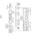
- FIG. 4 is a view illustrating an example of an internal jitter tolerance tester with internal accumulated jitter generator according to an exemplary embodiment of the present invention.
- a pseudorandom binary sequence (PRBS) generator may generate 1 and -1 randomly and a subsequent accumulator may accumulate a random signal.
- a lowpass filter may be used to eliminate a high frequency spur and a quantization noise.
- a pattern checker generates jitter-less input data and a pattern checker confirms the recovered data. By monitoring the bit-error-rate of the recovered data, the jitter tolerance specification of the CDR can be measured.
- the internal jitter tolerance tester with an internal jitter generator may include a loop filter with a predetermined gain ⁇ and a predetermined delay D , the internal accumulated jitter generator to generate an accumulated jitter, a gain multiplier to be connected to the loop filter and the internal accumulated jitter generator, and the phase rotator controller to be connected to the gain multiplier.
- FIG. 5 is a view illustrating an example of a power spectral density function of a phase rotator output phase with and without the lowpass filter according to an exemplary embodiment of the present invention.
- the lowpass filter may be located between the PRBS generator and the accumulator or after the accumulator.
- a gain controller may control an amount of the accumulated jitter.
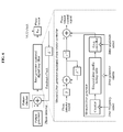
- FIG. 6 is a view illustrating an example of a sinusoid jitter generator equipped phase rotator controller according to an exemplary embodiment of the present invention.
- the accumulated jitter generator also may be replaced with the sinusoid jitter generator.
- a various CDRs' jitter tolerance performance under various conditions may be checked by selecting a frequency and an amplitude of the jitter.
- a pattern checker generates jitter-less input data and a pattern checker confirms the recovered data. By monitoring the bit-error-rate of the recovered data, the jitter tolerance specification of the CDR can be measured.
- the internal jitter tolerance tester with the internal jitter generator may include the loop filter with the predetermined gain ⁇ and the predetermined delay D , a sinusoid jitter generator to generate an accumulated jitter, the gain multiplier to be connected to the loop filter and the sinusoid jitter generator, and the phase rotator controller to be connected to the gain multiplier.
- a proposed archetecture may also be applied to any digitally-controlled-oscillator (DCO) based type-2 designs since a second order loop may be often overdamped and hence behave very similarly to a first-order loop.
- DCO digitally-controlled-oscillator
- FIG. 7 is a view illustration an example of a Z-domain block diagram of a DCO-based type-2 digital CDR according to an exemplary embodiment of the present invention.
- the phase step of the loop may be given by the following Equation 4.
- ⁇ vco K vco f 0 UI
- K vco may denote a DCO gain
- f 0 may denote a nominal frequency, respectively.
- ⁇ 0, only difference between a phase rotator-based CDR and a DCO-based CDR may be a location of the phase accumulator.
- FIG. 8 is a view illustration an example of an accumulated jitter generator equipped DCO controller according to an exemplary embodiment of the present invention.
- the accumulator may be eliminated from the accumulated jitter generator equipped phase rotator controller, since a DCO may operate as the phase accumulator.
- the internal jitter tolerance tester with a DCO may include the loop filter with a predetermined gain ⁇ and a predetermined delay D , the internal accumulated jitter generator to generate the accumulated jitter, the gain multiplier to be connected to the loop filter and the internal accumulated jitter generator, and the DCO to be connected to the gain multiplier.
- the internal jitter tolerance tester may include a digital loop filter consisting of a cyclic accumulator which accumulates a phase detector's output, a gain multiplier, an internal accumulated jitter generator (or internal sinusoid jitter generator), and a phase rotator (or DCO) controller.
- a digital loop filter consisting of a cyclic accumulator which accumulates a phase detector's output, a gain multiplier, an internal accumulated jitter generator (or internal sinusoid jitter generator), and a phase rotator (or DCO) controller.
- the internal accumulated jitter generator may include the PRBS generator, the digital loop filter, the accumulator, and the gain controller.
- the PRBS generator may generate 1 and -1 randomly and the subsequent accumulator may accumulate the random signal.
- the lowpass filter may be used to eliminate the high frequency spur and the quantization noise.
- the gain controller may control the amount of the accumulated jitter.
- the accumulated jitter generator also may be replaced with the sinusoid jitter generator.
- the internal sinusoid jitter generator may include a counter to select a frequency of a jitter from a sinusoid jitter profile lookup table, the sinusoid jitter profile lookup table, and a gain controller.
- the size of the counter may be proportional to a maximum period of the sinusoid jitter and the frequency of the sinusoid jitter may be controlled by selecting a size of the counter's counting step, while maintaining the clock frequency.
- the counter number may select a value of the jitter from the sinusoid jitter profile lookup table, and the gain controller may control the amplitude of the jitter.
- the exemplary embodiments according to the present invention may be recorded in computer-readable media including program instructions to implement various operations embodied by a computer.
- the media may also include, alone or in combination with the program instructions, data files, data structures, and the like.
- the media and program instructions may be those specially designed and constructed for the purposes of the present invention, or they may be of the kind well-known and available to those having skill in the computer software arts.
- the internal jitter generator also may be used as a jitter-equipped pattern generator.
- FIG. 9 is a view illustration an example of a jitter tolerance test method by using the accumulated jitter-equipped pattern generator.
- the jitter generator equipped digital loop filter and a phase rotator can generate a jitter-equipped clock signal and the jitter-equipped pattern can generated by using the clock as the sync clock of a pattern generator.
- the jitter tolerance spec of a target CDR can be measured by using the jitter-equipped pattern.
Landscapes
- Engineering & Computer Science (AREA)
- Physics & Mathematics (AREA)
- Computer Networks & Wireless Communication (AREA)
- Signal Processing (AREA)
- General Physics & Mathematics (AREA)
- Quality & Reliability (AREA)
- Nonlinear Science (AREA)
- General Engineering & Computer Science (AREA)
- Stabilization Of Oscillater, Synchronisation, Frequency Synthesizers (AREA)
- Dc Digital Transmission (AREA)
- Manipulation Of Pulses (AREA)
- Synchronisation In Digital Transmission Systems (AREA)
Abstract
Description
- Exemplary embodiments of the present invention relate to a jitter tolerance test.
- The input jitter of a clock and data recovery (CDR) can be modeled as the sum of the accumulated and non-accumulative jitter. The non-accumulative period jitter does not accumulate over time and has bounded variance in general. Data-dependent deterministic jitter is a subset of the non-accumulative jitter. The accumulated jitter, on the contrary, is unbounded in nature and increases indefinitely with time.
- A jitter tolerance mask provides the information on the accumulated and random non-accumulative jitter of a serial link.
- Even if the practical jitter in a link is hardly composed of sinusoids, the jitter tolerance specification is defined with sinusoids for testing purpose. In practice, the jitter in serial links carrying real traffic is more like random noise.
- An exemplary embodiment of the present invention discloses An internal jitter tolerance tester with an internal jitter generator, the jitter tolerance tester comprising a loop filter with a predetermined gain and a predetermined delay, an internal accumulated jitter generator to generate an accumulated jitter, a gain multiplier to be connected to the loop filter and the internal accumulated jitter generator, and a phase rotator controller to be connected to the gain multiplier.
- The internal accumulated jitter generator comprises a pseudorandom binary sequence (PRBS) generator to generate 1 and -1 randomly.
- The internal accumulated jitter generator further comprises a subsequent accumulator to accumulate a random signal.
- The internal accumulated jitter generator further comprises a lowpass filter to eliminate a high frequency spur and a quantization noise.
- The internal accumulated jitter generator further comprises a gain controller to control an amount of the accumulated jitter.
- Another exemplary embodiment of the present invention discloses an internal jitter tolerance tester with an internal jitter generator, the jitter tolerance tester comprising a loop filter with a predetermined gain and a predetermined delay, an internal sinusoid jitter generator to generate a sinusoid jitter, a gain multiplier to be connected to the loop filter and the sinusoid jitter generator, and a phase rotator controller to be connected to the gain multiplier.
- The sinusoid jitter generator comprises a counter to select a frequency of a jitter from a sinusoid jitter profile lookup table.
- The sinusoid jitter generator further comprises a gain controller to control amplitude of the jitter.
- Another exemplary embodiment of the present invention discloses an internal jitter tolerance tester with a DCO (digitally controlled oscillator), the jitter tolerance tester comprising a loop filter with a predetermined gain and a predetermined delay, an internal accumulated jitter generator to generate an accumulated jitter, a gain multiplier to be connected to the loop filter and the internal accumulated jitter generator, and a DCO to be connected to the gain multiplier.
- The internal accumulated jitter generator comprises a PRBS generator to generate 1 and -1 randomly.
- The internal accumulated jitter generator further comprises a lowpass filter to eliminate a high frequency spur and a quantization noise.
- The internal accumulated jitter generator further comprises a gain controller to control an amount of the accumulated jitter.
- The accompanying drawings, which are included to provide a further understanding of the invention and are incorporated in and constitute a part of this specification, illustrate embodiments of the invention, and together with the description serve to explain the principles of the invention.
-
FIG. 1 shows a Z-domain block diagram of a typical rotator-based CDR with a clock generator. -
FIG. 2 shows a discrete time model of input jitter. -
FIG. 3 show a typical shape of jitter tolerance mask. -
FIG. 4 is a view illustrating an example of an internal jitter tolerance tester with internal accumulated jitter generator according to an exemplary embodiment of the present invention. -
FIG. 5 is a view illustrating an example of a power spectral density function of a phase rotator output phase with and without the lowpass filter according to an exemplary embodiment of the present invention. -
FIG. 6 is a view illustrating an example of an internal jitter tolerance tester with internal sinusoid jitter generator according to an exemplary embodiment of the present invention. -
FIG. 7 is a view illustration an example of a Z-domain block diagram of a DCO-based type-2 digital CDR according to an exemplary embodiment of the present invention. -
FIG. 8 is a view illustration an example of an accumulated jitter generator equipped DCO controller according to an exemplary embodiment of the present invention. -
FIG. 9 is a view illustration an example of a jitter tolerance test method by using the accumulated jitter-equipped pattern generator. - The invention is described more fully hereinafter with reference to the accompanying drawings, in which exemplary embodiments of the invention are shown. This invention may, however, be embodied in many different forms and should not be construed as limited to the embodiments set forth herein. Rather, these exemplary embodiments are provided so that this disclosure is thorough, and will fully convey the scope of the invention to those skilled in the art. In the drawings, the size and relative sizes of layers and regions may be exaggerated for clarity. Like reference numerals in the drawings denote like elements.
-
FIG. 1 shows a Z-domain block diagram of a typical rotator-based CDR with a clock generator. The clock generator may provide frequency locked clocks to a digitally controlled phase rotator. The CDR model may consist of a phase detector, a loop filter with a gain β and a delay D, respectively, and the digitally controlled phase rotator. The gain of a phase rotator θ pr may be related to its resolution, as given by the followingEquation 1.
wherein the rotator resolution may be a reciprocal number of the phase rotator's minimum step size. - An input jitter of the CDR may be modeled as a sum of an accumulated and a non-accumulative period jitter. The non-accumulative period jitter may not accumulate over time and have bounded variance in general. A data-dependent deterministic jitter may be a subset of the non-accumulative jitter. The accumulated jitter, on the contrary, may be unbounded in nature and increase indefinitely with time, thus the CDR may have to track it for bit-error-free operation.
-
FIG. 2 shows a discrete time model of input jitter of the CDR. φ d,n and Nn may denote the accumulated and non-accumulative period jitter, respectively, at time index n. The accumulated jitter may be modeled by a discrete time random walk process. By using the Z-transform, a power spectral density of the accumulated jitter may given by the following Equation 2.
wherein E[W 2] may be a variance of random period jitter W, and fData may be a data rate. The Equation 2 may be simplified to the followingEquation 3 by the bilinear transformation.
wherein S(f) may decrease by -20dB/decade as frequency increases. -
FIG. 3 show a typical shape of jitter tolerance mask. The jitter tolerance mask may provide an information on the accumulated and a random non-accumulative period jitter of a serial link. The accumulated jitter may dominate at low frequencies and decrease by -20dB/decade as frequency increases. In a SONET jitter tolerance mask, a magnitude of the random non-accumulative period jitter may intersect with the accumulated jitter at 1/2500th of the data rate. - A magnitude of S(f) may be estimated with the jitter tolerance mask since the jitter tolerance mask may represent the maximum permissible jitter present in a communication link. Even if a practical jitter in the communication link may be hardly composed of sinusoids, the jitter tolerance specification may be defined with sinusoids for testing purposes. In practice, the jitter in serial links carrying real traffic may be more like random noise.
- Appropriate values for σ W and σ N may be estimated by matching the variances of the modeled jitter in the above
Fig. 2 with the variances of a sinusoid defined in the jitter tolerance mask. The magnitude of the jitter tolerance mask may be J(f), and W and N may be white Gaussian processes. |S(f)| may satisfy |S(f)| = |J(f)|2/8. ForaSONETjitter mask, σ W may be
- A creation of real world data traffic containing random accumulated jitter may be challenging in a lab enviromment. However, since the input jitter is a relative value between an input data phase and a recovered clock phase, a combination of a jittery recovered clock and a clean input data, and a combination of a jittery input data and a clean recovered clock may be in an unity inverse relationship, which magnitude may be same but direction may be opposite.
-
FIG. 4 is a view illustrating an example of an internal jitter tolerance tester with internal accumulated jitter generator according to an exemplary embodiment of the present invention. A pseudorandom binary sequence (PRBS) generator may generate 1 and -1 randomly and a subsequent accumulator may accumulate a random signal. A lowpass filter may be used to eliminate a high frequency spur and a quantization noise. A pattern checker generates jitter-less input data and a pattern checker confirms the recovered data. By monitoring the bit-error-rate of the recovered data, the jitter tolerance specification of the CDR can be measured. - In accordance with an example of the present invention, the internal jitter tolerance tester with an internal jitter generator may include a loop filter with a predetermined gain β and a predetermined delay D, the internal accumulated jitter generator to generate an accumulated jitter, a gain multiplier to be connected to the loop filter and the internal accumulated jitter generator, and the phase rotator controller to be connected to the gain multiplier.
-
FIG. 5 is a view illustrating an example of a power spectral density function of a phase rotator output phase with and without the lowpass filter according to an exemplary embodiment of the present invention. The lowpass filter may be located between the PRBS generator and the accumulator or after the accumulator. A gain controller may control an amount of the accumulated jitter. -
FIG. 6 is a view illustrating an example of a sinusoid jitter generator equipped phase rotator controller according to an exemplary embodiment of the present invention. The accumulated jitter generator also may be replaced with the sinusoid jitter generator. A various CDRs' jitter tolerance performance under various conditions may be checked by selecting a frequency and an amplitude of the jitter. A pattern checker generates jitter-less input data and a pattern checker confirms the recovered data. By monitoring the bit-error-rate of the recovered data, the jitter tolerance specification of the CDR can be measured. - In accordance with an example of the present invention, the internal jitter tolerance tester with the internal jitter generator may include the loop filter with the predetermined gain β and the predetermined delay D, a sinusoid jitter generator to generate an accumulated jitter, the gain multiplier to be connected to the loop filter and the sinusoid jitter generator, and the phase rotator controller to be connected to the gain multiplier.
- A proposed archetecture may also be applied to any digitally-controlled-oscillator (DCO) based type-2 designs since a second order loop may be often overdamped and hence behave very similarly to a first-order loop.
-
FIG. 7 is a view illustration an example of a Z-domain block diagram of a DCO-based type-2 digital CDR according to an exemplary embodiment of the present invention. The phase step of the loop may be given by the followingEquation 4.
wherein Kvco may denote a DCO gain and f 0 may denote a nominal frequency, respectively. In the case of α = 0, only difference between a phase rotator-based CDR and a DCO-based CDR may be a location of the phase accumulator. -
FIG. 8 is a view illustration an example of an accumulated jitter generator equipped DCO controller according to an exemplary embodiment of the present invention.. The accumulator may be eliminated from the accumulated jitter generator equipped phase rotator controller, since a DCO may operate as the phase accumulator. - In accordance with an example of the present invention, the internal jitter tolerance tester with a DCO (digitally controlled oscillator) may include the loop filter with a predetermined gain β and a predetermined delay D, the internal accumulated jitter generator to generate the accumulated jitter, the gain multiplier to be connected to the loop filter and the internal accumulated jitter generator, and the DCO to be connected to the gain multiplier.
- The internal jitter tolerance tester may include a digital loop filter consisting of a cyclic accumulator which accumulates a phase detector's output, a gain multiplier, an internal accumulated jitter generator (or internal sinusoid jitter generator), and a phase rotator (or DCO) controller.
- The internal accumulated jitter generator may include the PRBS generator, the digital loop filter, the accumulator, and the gain controller. The PRBS generator may generate 1 and -1 randomly and the subsequent accumulator may accumulate the random signal. The lowpass filter may be used to eliminate the high frequency spur and the quantization noise. The gain controller may control the amount of the accumulated jitter.
- The accumulated jitter generator also may be replaced with the sinusoid jitter generator. The internal sinusoid jitter generator may include a counter to select a frequency of a jitter from a sinusoid jitter profile lookup table, the sinusoid jitter profile lookup table, and a gain controller. The size of the counter may be proportional to a maximum period of the sinusoid jitter and the frequency of the sinusoid jitter may be controlled by selecting a size of the counter's counting step, while maintaining the clock frequency. The counter number may select a value of the jitter from the sinusoid jitter profile lookup table, and the gain controller may control the amplitude of the jitter.
- The exemplary embodiments according to the present invention may be recorded in computer-readable media including program instructions to implement various operations embodied by a computer. The media may also include, alone or in combination with the program instructions, data files, data structures, and the like. The media and program instructions may be those specially designed and constructed for the purposes of the present invention, or they may be of the kind well-known and available to those having skill in the computer software arts.
- It will be apparent to those skilled in the art that various modifications and variation can be made in the present invention without departing from the spirit or scope of the invention. Thus, it is intended that the present invention cover the modifications and variations of this invention provided they come within the scope of the appended claims and their equivalents.
- The internal jitter generator also may be used as a jitter-equipped pattern generator.
FIG. 9 is a view illustration an example of a jitter tolerance test method by using the accumulated jitter-equipped pattern generator. The jitter generator equipped digital loop filter and a phase rotator can generate a jitter-equipped clock signal and the jitter-equipped pattern can generated by using the clock as the sync clock of a pattern generator. The jitter tolerance spec of a target CDR can be measured by using the jitter-equipped pattern.
Claims (12)
- An internal jitter tolerance tester with an internal jitter generator, the jitter tolerance tester comprising:a loop filter with a predetermined gain and a predetermined delay;an internal accumulated jitter generator to generate an accumulated jitter;a gain multiplier to be connected to the loop filter and the internal accumulated jitter generator; anda phase rotator controller to be connected to the gain multiplier.
- The internal jitter tolerance tester of claim 1, wherein the internal accumulated jitter generator comprises,
a pseudorandom binary sequence (PRBS) generator to generate 1 and -1 randomly. - The internal jitter tolerance tester of claim 2, wherein the internal accumulated jitter generator further comprises,
a subsequent accumulator to accumulate a random signal. - The internal jitter tolerance tester of claim 3, wherein the internal accumulated jitter generator further comprises,
a lowpass filter to eliminate a high frequency spur and a quantization noise. - The internal jitter tolerance tester of claim 4, wherein the internal accumulated jitter generator further comprises,
a gain controller to control an amount of the accumulated jitter. - An internal jitter tolerance tester with an internal jitter generator, the jitter tolerance tester comprising:a loop filter with a predetermined gain and a predetermined delay;an internal sinusoid jitter generator to generate a sinusoid jitter;a gain multiplier to be connected to the loop filter and the sinusoid jitter generator; anda phase rotator controller to be connected to the gain multiplier.
- The internal jitter tolerance tester of claim 6, wherein the sinusoid jitter generator comprises,
a counter to select a frequency of a jitter from a sinusoid jitter profile lookup table. - The internal jitter tolerance tester of claim 7, wherein the sinusoid jitter generator further comprises,
a gain controller to control an amplitude of the jitter. - An internal jitter tolerance tester with a DCO (digitally controlled oscillator), the jitter tolerance tester comprising:a loop filter with a predetermined gain and a predetermined delay;an internal accumulated jitter generator to generate an accumulated jitter;a gain multiplier to be connected to the loop filter and the internal accumulated jitter generator; anda DCO to be connected to the gain multiplier.
- The internal jitter tolerance tester of claim 9, wherein the internal accumulated jitter generator comprises,
a PRBS generator to generate 1 and -1 randomly. - The internal jitter tolerance tester of claim 10, wherein the internal accumulated jitter generator further comprises,
a lowpass filter to eliminate a high frequency spur and a quantization noise. - The internal jitter tolerance tester of claim 11, wherein the internal accumulated jitter generator further comprises,
a gain controller to control an amount of the accumulated jitter.
Applications Claiming Priority (1)
| Application Number | Priority Date | Filing Date | Title |
|---|---|---|---|
| US14/070,249 US9065653B2 (en) | 2013-11-01 | 2013-11-01 | Internal jitter tolerance tester with an internal jitter generator |
Publications (2)
| Publication Number | Publication Date |
|---|---|
| EP2876835A2 true EP2876835A2 (en) | 2015-05-27 |
| EP2876835A3 EP2876835A3 (en) | 2015-09-30 |
Family
ID=51900111
Family Applications (1)
| Application Number | Title | Priority Date | Filing Date |
|---|---|---|---|
| EP14191248.5A Withdrawn EP2876835A3 (en) | 2013-11-01 | 2014-10-31 | Internal jitter tolerance tester with an internal jitter generator |
Country Status (5)
| Country | Link |
|---|---|
| US (1) | US9065653B2 (en) |
| EP (1) | EP2876835A3 (en) |
| JP (1) | JP5993918B2 (en) |
| KR (1) | KR101584454B1 (en) |
| CN (1) | CN104617938A (en) |
Families Citing this family (5)
| Publication number | Priority date | Publication date | Assignee | Title |
|---|---|---|---|---|
| US7917798B2 (en) | 2005-10-04 | 2011-03-29 | Hypres, Inc. | Superconducting digital phase rotator |
| CN113691241B (en) * | 2021-08-11 | 2022-03-15 | 电子科技大学 | High-precision digital jitter injection device based on amplitude conversion time sequence |
| KR102833443B1 (en) | 2021-09-13 | 2025-07-10 | 삼성전자주식회사 | Pattern generator and built-in-self test device including the same |
| CN114785712B (en) * | 2022-06-16 | 2022-09-20 | 中星联华科技(北京)有限公司 | Error code meter-based jitter tolerance testing method and device and electronic equipment |
| CN116248542B (en) * | 2023-05-12 | 2023-08-08 | 芯耀辉科技有限公司 | Device, method and system for jitter tolerance test in digital communication |
Family Cites Families (10)
| Publication number | Priority date | Publication date | Assignee | Title |
|---|---|---|---|---|
| NL8800119A (en) * | 1988-01-19 | 1989-08-16 | Catena Microelect Bv | VOLTAGE CONTROLLED OSCILLATOR. |
| JPH10224213A (en) * | 1997-02-03 | 1998-08-21 | Anritsu Corp | Jitter generator using pll circuit |
| JP2005198120A (en) * | 2004-01-09 | 2005-07-21 | Yokogawa Electric Corp | Jitter generator |
| CN100347962C (en) * | 2004-03-31 | 2007-11-07 | 清华大学 | Method for removing phase noise for time domain synchronous or thogonal frequency-division multiplex receiver and system and thereof |
| WO2008115968A1 (en) * | 2007-03-20 | 2008-09-25 | Rambus Incorporated | Integrated circuit having receiver jitter tolerance ('jtol') measurement |
| US8045670B2 (en) * | 2007-06-22 | 2011-10-25 | Texas Instruments Incorporated | Interpolative all-digital phase locked loop |
| DE112008002591B4 (en) * | 2007-09-28 | 2016-12-15 | Anritsu Corp. | Jitter generating device, device testing system using the same, and jitter generating method |
| US8269563B2 (en) * | 2008-06-10 | 2012-09-18 | Qualcomm Incorporated | Dithering a digitally-controlled oscillator output in a phase-locked loop |
| JP2010199934A (en) * | 2009-02-25 | 2010-09-09 | Yokogawa Electric Corp | Jitter generating apparatus |
| US8938043B2 (en) * | 2012-03-29 | 2015-01-20 | Terasquare Co., Ltd. | Adaptive optimum CDR bandwidth estimation by using a kalman gain extractor |
-
2013
- 2013-11-01 US US14/070,249 patent/US9065653B2/en active Active
-
2014
- 2014-10-20 KR KR1020140141667A patent/KR101584454B1/en active Active
- 2014-10-30 CN CN201410601545.8A patent/CN104617938A/en active Pending
- 2014-10-31 EP EP14191248.5A patent/EP2876835A3/en not_active Withdrawn
- 2014-10-31 JP JP2014223499A patent/JP5993918B2/en active Active
Non-Patent Citations (1)
| Title |
|---|
| None |
Also Published As
| Publication number | Publication date |
|---|---|
| JP2015089139A (en) | 2015-05-07 |
| CN104617938A (en) | 2015-05-13 |
| KR20150051313A (en) | 2015-05-12 |
| KR101584454B1 (en) | 2016-01-25 |
| US9065653B2 (en) | 2015-06-23 |
| JP5993918B2 (en) | 2016-09-14 |
| EP2876835A3 (en) | 2015-09-30 |
| US20150124861A1 (en) | 2015-05-07 |
Similar Documents
| Publication | Publication Date | Title |
|---|---|---|
| US9065653B2 (en) | Internal jitter tolerance tester with an internal jitter generator | |
| US8284886B2 (en) | Radio frequency built-in self test for quality monitoring of local oscillator and transmitter | |
| Da Dalt | Linearized analysis of a digital bang-bang PLL and its validity limits applied to jitter transfer and jitter generation | |
| Mojiri et al. | Processing of harmonics and interharmonics using an adaptive notch filter | |
| Da Dalt | Markov chains-based derivation of the phase detector gain in bang-bang PLLs | |
| Park et al. | Pseudo-linear analysis of bang-bang controlled timing circuits | |
| US20130259178A1 (en) | Adaptive optimum cdr bandwidth estimation by using a kalman gain extractor | |
| Yang et al. | On-chip jitter measurement for true random number generators | |
| Chen et al. | Single-event transient induced harmonic errors in digitally controlled ring oscillators | |
| WO2020112277A1 (en) | Systems and methods for mitigation of nonlinearity related phase noise degradations | |
| CN110739964A (en) | Self-testing phase-locked loops using pseudo-random noise | |
| US20230184828A1 (en) | Method and Apparatus for Analyzing Phase Noise in a Signal from an Electronic Device | |
| US10069502B2 (en) | Method for PPL and CDR designs for achieving specific bandwidth and phase margin requirements | |
| Tertinek et al. | Statistical analysis of first-order bang-bang phase-locked loops using sign-dependent random-walk theory | |
| DE102005050621B4 (en) | Phase-locked loop and method for operating a phase locked loop | |
| WO2006000512A1 (en) | Reduction of the settling time and compensation of phase errors of frequency synthesizers based on phase-locking loops | |
| Muhammad et al. | Verification of digital RF processors: RF, analog, baseband, and software | |
| CN104426543A (en) | Output clock generation method and device thereof | |
| CN1838584B (en) | Signal jitter measuring method and device | |
| DE102013213385A1 (en) | Method for evaluating an output of a random number generator | |
| DE102013213392A1 (en) | Method for evaluating an output of a random number generator | |
| Ugarte et al. | High-order PLL design with constant phase margin | |
| Hungenberg et al. | Automatic relocking of an FPGA-based PID controller using a bandpass-filtering approach | |
| Vamvakos et al. | Discrete-time, cyclostationary phase-locked loop model for jitter analysis | |
| Chowdhury et al. | A probabilistic test instrument using a ΣΔ-encoded amplitude/phase-signal generation technique |
Legal Events
| Date | Code | Title | Description |
|---|---|---|---|
| PUAI | Public reference made under article 153(3) epc to a published international application that has entered the european phase |
Free format text: ORIGINAL CODE: 0009012 |
|
| 17P | Request for examination filed |
Effective date: 20141119 |
|
| AK | Designated contracting states |
Kind code of ref document: A2 Designated state(s): AL AT BE BG CH CY CZ DE DK EE ES FI FR GB GR HR HU IE IS IT LI LT LU LV MC MK MT NL NO PL PT RO RS SE SI SK SM TR |
|
| AX | Request for extension of the european patent |
Extension state: BA ME |
|
| PUAL | Search report despatched |
Free format text: ORIGINAL CODE: 0009013 |
|
| AK | Designated contracting states |
Kind code of ref document: A3 Designated state(s): AL AT BE BG CH CY CZ DE DK EE ES FI FR GB GR HR HU IE IS IT LI LT LU LV MC MK MT NL NO PL PT RO RS SE SI SK SM TR |
|
| AX | Request for extension of the european patent |
Extension state: BA ME |
|
| RIC1 | Information provided on ipc code assigned before grant |
Ipc: G01R 31/317 20060101ALI20150821BHEP Ipc: H04L 1/20 20060101AFI20150821BHEP Ipc: H04L 1/24 20060101ALI20150821BHEP |
|
| RAP1 | Party data changed (applicant data changed or rights of an application transferred) |
Owner name: KOREA ADVANCED INSTITUTE OF SCIENCE AND TECHNOLOGY Owner name: GIGOPTIX-TERASQUARE KOREA CO., LTD. |
|
| RBV | Designated contracting states (corrected) |
Designated state(s): AL AT BE BG CH CY CZ DE DK EE ES FI FR GB GR HR HU IE IS IT LI LT LU LV MC MK MT NL NO PL PT RO RS SE SI SK SM TR |
|
| RAP3 | Party data changed (applicant data changed or rights of an application transferred) |
Owner name: KOREA ADVANCED INSTITUTE OF SCIENCE AND TECHNOLOGY Owner name: GIGOPTIX-TERASQUARE KOREA CO., LTD. |
|
| GRAP | Despatch of communication of intention to grant a patent |
Free format text: ORIGINAL CODE: EPIDOSNIGR1 |
|
| STAA | Information on the status of an ep patent application or granted ep patent |
Free format text: STATUS: GRANT OF PATENT IS INTENDED |
|
| INTG | Intention to grant announced |
Effective date: 20180813 |
|
| STAA | Information on the status of an ep patent application or granted ep patent |
Free format text: STATUS: THE APPLICATION IS DEEMED TO BE WITHDRAWN |
|
| 18D | Application deemed to be withdrawn |
Effective date: 20190103 |