EP2871747A1 - Charging apparatus - Google Patents
Charging apparatus Download PDFInfo
- Publication number
- EP2871747A1 EP2871747A1 EP20130812460 EP13812460A EP2871747A1 EP 2871747 A1 EP2871747 A1 EP 2871747A1 EP 20130812460 EP20130812460 EP 20130812460 EP 13812460 A EP13812460 A EP 13812460A EP 2871747 A1 EP2871747 A1 EP 2871747A1
- Authority
- EP
- European Patent Office
- Prior art keywords
- current
- charging
- small
- charging circuit
- storage battery
- Prior art date
- Legal status (The legal status is an assumption and is not a legal conclusion. Google has not performed a legal analysis and makes no representation as to the accuracy of the status listed.)
- Granted
Links
Images

Classifications
-
- H—ELECTRICITY
- H02—GENERATION; CONVERSION OR DISTRIBUTION OF ELECTRIC POWER
- H02J—ELECTRIC POWER NETWORKS; CIRCUIT ARRANGEMENTS OR SYSTEMS FOR SUPPLYING OR DISTRIBUTING ELECTRIC POWER; SYSTEMS FOR STORING ELECTRIC ENERGY
- H02J7/00—Circuit arrangements for charging or discharging batteries or for supplying loads from batteries
-
- H—ELECTRICITY
- H02—GENERATION; CONVERSION OR DISTRIBUTION OF ELECTRIC POWER
- H02J—ELECTRIC POWER NETWORKS; CIRCUIT ARRANGEMENTS OR SYSTEMS FOR SUPPLYING OR DISTRIBUTING ELECTRIC POWER; SYSTEMS FOR STORING ELECTRIC ENERGY
- H02J7/00—Circuit arrangements for charging or discharging batteries or for supplying loads from batteries
- H02J7/02—Circuit arrangements for charging or discharging batteries or for supplying loads from batteries for charging batteries from AC mains by converters
- H02J7/04—Regulation of charging current or voltage
-
- H—ELECTRICITY
- H02—GENERATION; CONVERSION OR DISTRIBUTION OF ELECTRIC POWER
- H02J—ELECTRIC POWER NETWORKS; CIRCUIT ARRANGEMENTS OR SYSTEMS FOR SUPPLYING OR DISTRIBUTING ELECTRIC POWER; SYSTEMS FOR STORING ELECTRIC ENERGY
- H02J7/00—Circuit arrangements for charging or discharging batteries or for supplying loads from batteries
- H02J7/90—Regulation of charging or discharging current or voltage
-
- H—ELECTRICITY
- H02—GENERATION; CONVERSION OR DISTRIBUTION OF ELECTRIC POWER
- H02J—ELECTRIC POWER NETWORKS; CIRCUIT ARRANGEMENTS OR SYSTEMS FOR SUPPLYING OR DISTRIBUTING ELECTRIC POWER; SYSTEMS FOR STORING ELECTRIC ENERGY
- H02J2207/00—Details of circuit arrangements for charging or discharging batteries or supplying loads from batteries
- H02J2207/20—Charging or discharging characterised by the power electronics converter
Definitions
- the present invention relates to a charging apparatus that charges a storage battery of an electric device or the like.
- a known charging apparatus includes a large-current charging circuit, which charges a storage battery with a large current, and a small-current charging circuit, which charges a storage battery with a small current (e.g., refer to patent document 1).
- a charging apparatus of patent document 1 includes two independent transformers, each including two types of secondary coils to selectively generate large and small charging currents. Subsequent stages of the two transformers include a large number of switching elements, which switches charging lines so that the charging current supplied to a storage battery can be selectively switched between large and small currents.
- Patent Document 1 Japanese Laid-Open Patent Publication No. 56-53550
- such a charging apparatus that is described above includes two independent transformers, each including two types of secondary coils. This results in the two transformers having complicated and enlarged structures, which, in turn, results in the charging apparatus having a completed and enlarged structure.
- the charging apparatus includes a charging terminal used to connect a storage battery, a large-current charging circuit that generates a first charging current, a small-current charging circuit that generates a second charging current that is smaller than the first charging current, a switching element selectively connecting the large-current charging circuit to the charging terminal, and a power terminal.
- the large-current charging circuit and the small-current charging circuit are connected in series between the power terminal and the charging terminal.
- the charging apparatus includes a line switching controller that detects a voltage of the storage battery.
- the line switching controller activates the switching element when a detected voltage is smaller than a predetermined value, and deactivates the switching element when the detected voltage is larger than or equal to the predetermined value.
- the small-current charging circuit includes a current controlling IC that detects the voltage of the storage battery and variably controls a charging current in a linear manner in accordance with a detected voltage.
- the small-current charging circuit includes a current controlling IC that detects the voltage of the storage battery and variably controls a charging current in a plurality of steps in accordance with a detected voltage.
- the small-current charging circuit includes a resistor connected between the large-current charging circuit and the charging terminal.
- the small-current charging circuit includes a small-current switching element connected between the large-current charging circuit and the charging terminal, and the line switching controller PWM-controls the small-current switching element to vary a charging current in a linear manner.
- the small-current charging circuit includes a small-current switching element connected between the large-current charging circuit and the charging terminal, and the line switching controller PWM-controls the small-current switching element to vary a charging current in a plurality of steps.
- the present invention provides a charging apparatus that performs charging selectively with a large current and a small current, while allowing for reduction in size and a simplified structure.
- a charging apparatus includes a large-current charging circuit 1, a small-current charging circuit 2, a switch unit 3, and a line switching controller 4.
- the large-current charging circuit 1 and the small-current charging circuit 2 are connected in series between two power terminals 5a and 5b and two charging terminals 6a and 6b.
- the large-current charging circuit 1 includes an adapter having a transformer (not shown). A primary coil of the transformer is connected to an alternating current power supply 7 through the two power terminals 5a and 5b.
- a secondary coil of the transformer includes a first terminal, which is connected to the small-current charging circuit 2 by a high-potential wire 8 and a Schottky diode D, and a second terminal, which is connected to the small-current charging circuit 2 and the low-potential charging terminal 6b by a low-potential wire 9.
- the small-current charging circuit 2 includes a current controlling IC 10.
- the current controlling IC 10 is connected to the high-potential charging terminal 6a by the high-potential wire 8.
- the current controlling IC 10 is connected to the low-potential charging terminal 6b by the low-potential wire 9.
- the current controlling IC 10 converts a large charging current received from the large-current charging circuit 1 to a small charging current to supply the charging current to the two charging terminals 6a and 6b.
- the current controlling IC 10 detects the voltage of a storage battery 11, which is connected to the two charging terminals 6a and 6b, and variably controls the charging current in a non-stepped (linear) manner in accordance with a detected voltage. More specifically, the current controlling IC 10 supplies the two charging terminals 6a and 6b and, ultimately, the storage battery 11 with a smaller charging current as the detected voltage increases.
- the large-current charging circuit 1 is connected to the charging terminal 6a by the switch unit 3.
- the switch unit 3 includes a p-channel field-effect transistor (FET) 12, which serves as a switching element.
- FET field-effect transistor
- the cathode of the Schottky diode D is connected to the small-current charging circuit 2 by the high-potential wire 8.
- a connection point of the Schottky diode D and the small-current charging circuit 2 is connected to the high-potential charging terminal 6a by the FET 12.
- a resistor R1 is connected between the gate and the source of the FET 12.
- the gate of the FET 12 is connected to the low-potential wire 9 (charging terminal 6b) by a transistor 13, which will be described later.
- the line switching controller 4 includes an NPN-type transistor 13 and a microcontroller 14.
- the line switching controller 4 detects the voltage of the storage battery 11.
- the line switching controller 4 activates the FET 12 when the detected voltage is smaller than a predetermined value, and deactivates the FET 12 when the detected voltage is larger than or equal to the predetermined value.
- the microcontroller 14 is connected to the two charging terminals 6a and 6b and also connected to the base of the transistor 13 by a resistor R2.
- the microcontroller 14 detects the voltage of the storage battery 11.
- the microcontroller 14 supplies a base current to the transistor 13, only when the detected voltage is smaller than the predetermined value, to activate the transistor 13 in order to activate the FET 12.
- a resistor R3 is connected between the base and the emitter of the transistor 13.
- the storage battery 11 having an extremely low state of charge is connected to the two charging terminals 6a and 6b.
- the microcontroller 14 supplies the base current to the transistor 13. This activates the transistor 13, which, in turn, activates the FET 12.
- the large-current charging circuit 1 directly supplies the storage battery 11 with a large charging current through the FET 12 (without the current flowing through the small-current charging circuit 2).
- the storage battery 11 is charged with a large charging current.
- the storage battery 11 having a relatively large state of charge may be connected to the two charging terminals 6a and 6b, or a predetermined time may elapse after the storage battery 11 is charged with a large charging current as described above.
- the microcontroller 14 stops supplying the base current to the transistor 13. This deactivates the transistor 13, which, in turn, activates the FET 12.
- the current controlling IC 10 converts a large charging current received from the large-current charging circuit 1 to a small charging current (i.e., the current controlling IC 10 uses the output of the large-current charging circuit 1 as a power supply) to supply the small charging current to the storage battery 11.
- the storage battery 11 is charged with a small charging current.
- the current controlling IC 10 detects the voltage of the storage battery 11 and variably controls the charging current in a non-stepped manner in accordance with the detected voltage. More specifically, the current controlling IC 10 supplies the storage battery 11 with a smaller charging current as the detected voltage of the storage battery 11 increases.
- the small-current charging circuit 2 includes the current controlling IC 10.
- a different structure may be used as long as it has the same function.
- a small-current charging circuit 21 includes a resistor R11 connected between the large-current charging circuit 1 and the charging terminal 6a, a p-channel field-effect transistor (FET) 22 serving as a small-current switching element, and an NPN-type transistor 23 used to control the FET 22.
- FET field-effect transistor
- the high-potential wire 8 is connected to the high-potential charging terminal 6a by the FET 22 and the resistor R11.
- a resistor R12 is connected between the gate and the source of the FET 22.
- the gate of the FET 22 is connected to the low-potential wire 9 (charging terminal 6b) through the transistor 23.
- a transistor R13 is connected between the base and the emitter of the transistor 23.
- the microcontroller 14 is connected to the base of the transistor 23 through a transistor R14.
- the microcontroller 14 of this example supplies the base current to the transistor 23 to activate the transistor 23, which, in turn, activates the FET 22, only when the detected voltage of the storage battery 11 is larger than or equal to the predetermined value.
- the microcontroller 14 of this example PWM-controls the FET 22 based on the detected voltage of the storage battery 11 to variably control the charging current in a non-stepped manner. More specifically, as the detected voltage increases, the microcontroller 14 uses a smaller duty ratio to activate the FET 22 so that the storage battery 11 is charged with a small charging current.
- the small-current charging circuit 21 includes the resistor R1 connected between the large-current charging circuit 1 and the charging terminal 6a.
- a simple structure may be used to convert the large-current supplied from the large-current charging circuit 1 to a small charging current.
- the small-current charging circuit 21 includes the FET 22 connected between the large-current charging circuit 1 and the charging terminal 6a.
- the storage battery 11 may be charged in a further optimal manner as compared to when the storage battery 11 is charged with a constant small charging current.
- the cost may be reduced as compared to, for example, a structure using the dedicated current controlling IC 10 (refer to Fig. 1 ) to obtain the same advantages.
- the above embodiment includes the line switching controller 4 that activates the FET 12 (switching element) when the detected voltage of the storage battery 11 is smaller than the predetermined value, and deactivates the FET 12 when the detected voltage of the storage battery 11 is larger than or equal to the predetermined value.
- the configuration is not limited in such a manner and may be changed so that the FET 12 (switching element) is controlled by a different means.
- the configuration may be changed to include a controller that controls the switching element (FET 12) in accordance with the time elapsed from when charging is started.
- the configuration may be changed to allow a user to freely select and control the switching element (FET 12).
- the small-current charging circuit 2 (21) can variably control the charging current in a non-stepped manner in accordance with the detected voltage of the storage battery 11.
- the configuration is not limited in such a manner and may be changed to, for example, a small-current charging circuit that charges the storage battery 11 with a charging current of a constant small current value.
- the small-current charging circuit 2 (21) may be modified to variably control the charging current in a plurality of steps in accordance with the detected voltage of the storage battery 11.
- the above embodiment uses the FET 12 as the switching element, however, it may be changed to use a different switching element that has the same function.
Landscapes
- Engineering & Computer Science (AREA)
- Power Engineering (AREA)
- Charge And Discharge Circuits For Batteries Or The Like (AREA)
- Secondary Cells (AREA)
Abstract
Description
- The present invention relates to a charging apparatus that charges a storage battery of an electric device or the like.
- A known charging apparatus includes a large-current charging circuit, which charges a storage battery with a large current, and a small-current charging circuit, which charges a storage battery with a small current (e.g., refer to patent document 1). A charging apparatus of
patent document 1 includes two independent transformers, each including two types of secondary coils to selectively generate large and small charging currents. Subsequent stages of the two transformers include a large number of switching elements, which switches charging lines so that the charging current supplied to a storage battery can be selectively switched between large and small currents. - Patent Document 1: Japanese Laid-Open Patent Publication No.
56-53550 - However, such a charging apparatus that is described above includes two independent transformers, each including two types of secondary coils. This results in the two transformers having complicated and enlarged structures, which, in turn, results in the charging apparatus having a completed and enlarged structure.
- It is an object of the present invention to provide a charging apparatus that performs charging selectively with a large current and a small current, while allowing for reduction in size and a simplified structure.
- One aspect of the present invention is a charging apparatus. The charging apparatus includes a charging terminal used to connect a storage battery, a large-current charging circuit that generates a first charging current, a small-current charging circuit that generates a second charging current that is smaller than the first charging current, a switching element selectively connecting the large-current charging circuit to the charging terminal, and a power terminal. The large-current charging circuit and the small-current charging circuit are connected in series between the power terminal and the charging terminal.
- Preferably, the charging apparatus includes a line switching controller that detects a voltage of the storage battery. The line switching controller activates the switching element when a detected voltage is smaller than a predetermined value, and deactivates the switching element when the detected voltage is larger than or equal to the predetermined value.
- Preferably, in the charging apparatus, the small-current charging circuit includes a current controlling IC that detects the voltage of the storage battery and variably controls a charging current in a linear manner in accordance with a detected voltage.
- Preferably, in the charging apparatus, the small-current charging circuit includes a current controlling IC that detects the voltage of the storage battery and variably controls a charging current in a plurality of steps in accordance with a detected voltage.
- Preferably, in the charging apparatus, the small-current charging circuit includes a resistor connected between the large-current charging circuit and the charging terminal.
- Preferably, in the charging apparatus, the small-current charging circuit includes a small-current switching element connected between the large-current charging circuit and the charging terminal, and the line switching controller PWM-controls the small-current switching element to vary a charging current in a linear manner.
- Preferably, in the charging apparatus, the small-current charging circuit includes a small-current switching element connected between the large-current charging circuit and the charging terminal, and the line switching controller PWM-controls the small-current switching element to vary a charging current in a plurality of steps.
- The present invention provides a charging apparatus that performs charging selectively with a large current and a small current, while allowing for reduction in size and a simplified structure.
-
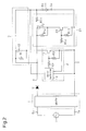
Fig. 1 is a circuit diagram showing one embodiment of a charging apparatus. -
Fig. 2 is a circuit diagram showing one example of a charging apparatus. - One embodiment of a charging apparatus according to the present invention will now be described with reference to
Fig. 1 . - As shown in
Fig. 1 , a charging apparatus includes a large-current charging circuit 1, a small-current charging circuit 2, aswitch unit 3, and aline switching controller 4. The large-current charging circuit 1 and the small-current charging circuit 2 are connected in series between twopower terminals charging terminals - More specifically, the large-
current charging circuit 1 includes an adapter having a transformer (not shown). A primary coil of the transformer is connected to an alternatingcurrent power supply 7 through the twopower terminals - A secondary coil of the transformer includes a first terminal, which is connected to the small-
current charging circuit 2 by a high-potential wire 8 and a Schottky diode D, and a second terminal, which is connected to the small-current charging circuit 2 and the low-potential charging terminal 6b by a low-potential wire 9. - The small-
current charging circuit 2 includes a current controllingIC 10. The current controlling IC 10 is connected to the high-potential charging terminal 6a by the high-potential wire 8. The current controllingIC 10 is connected to the low-potential charging terminal 6b by the low-potential wire 9. The current controllingIC 10 converts a large charging current received from the large-current charging circuit 1 to a small charging current to supply the charging current to the twocharging terminals IC 10 detects the voltage of astorage battery 11, which is connected to the twocharging terminals charging terminals storage battery 11 with a smaller charging current as the detected voltage increases. - The large-
current charging circuit 1 is connected to thecharging terminal 6a by theswitch unit 3. Theswitch unit 3 includes a p-channel field-effect transistor (FET) 12, which serves as a switching element. - More specifically, the cathode of the Schottky diode D is connected to the small-
current charging circuit 2 by the high-potential wire 8. A connection point of the Schottky diode D and the small-current charging circuit 2 is connected to the high-potential charging terminal 6a by the FET 12. A resistor R1 is connected between the gate and the source of theFET 12. The gate of theFET 12 is connected to the low-potential wire 9 (charging terminal 6b) by atransistor 13, which will be described later. - The
line switching controller 4 includes an NPN-type transistor 13 and amicrocontroller 14. Theline switching controller 4 detects the voltage of thestorage battery 11. Theline switching controller 4 activates theFET 12 when the detected voltage is smaller than a predetermined value, and deactivates theFET 12 when the detected voltage is larger than or equal to the predetermined value. - More specifically, the
microcontroller 14 is connected to the twocharging terminals transistor 13 by a resistor R2. Themicrocontroller 14 detects the voltage of thestorage battery 11. Themicrocontroller 14 supplies a base current to thetransistor 13, only when the detected voltage is smaller than the predetermined value, to activate thetransistor 13 in order to activate theFET 12. A resistor R3 is connected between the base and the emitter of thetransistor 13. - The operation of the charging apparatus will now be described.
- For example, the
storage battery 11 having an extremely low state of charge is connected to the twocharging terminals storage battery 11 is smaller than the predetermined value, themicrocontroller 14 supplies the base current to thetransistor 13. This activates thetransistor 13, which, in turn, activates theFET 12. - Then, the large-
current charging circuit 1 directly supplies thestorage battery 11 with a large charging current through the FET 12 (without the current flowing through the small-current charging circuit 2). Thus, thestorage battery 11 is charged with a large charging current. - For example, the
storage battery 11 having a relatively large state of charge may be connected to the twocharging terminals storage battery 11 is charged with a large charging current as described above. In such a case, when determining that the voltage of thestorage battery 11 is larger than or equal to the predetermined value, themicrocontroller 14 stops supplying the base current to thetransistor 13. This deactivates thetransistor 13, which, in turn, activates theFET 12. - Then, the current controlling
IC 10 converts a large charging current received from the large-current charging circuit 1 to a small charging current (i.e., the current controllingIC 10 uses the output of the large-current charging circuit 1 as a power supply) to supply the small charging current to thestorage battery 11. Thus, thestorage battery 11 is charged with a small charging current. In this case, the current controllingIC 10 detects the voltage of thestorage battery 11 and variably controls the charging current in a non-stepped manner in accordance with the detected voltage. More specifically, the current controlling IC 10 supplies thestorage battery 11 with a smaller charging current as the detected voltage of thestorage battery 11 increases. - Accordingly, the above embodiment has the advantages described below.
- (1) The large-
current charging circuit 1 and the small-current charging circuit 2, which are connected in series, are arranged between the twopower terminals charging terminals current charging circuit 1 and thecharging terminal 6a are connected by theFET 12, which functions as a switching element. Thus, for example, when theFET 12 is activated, thestorage battery 11 is directly charged with a large charging current from the large-current charging circuit 1. In contrast, when theFET 12 is deactivated, thestorage battery 11 is charged with a small charging current through the small-current charging circuit 2. In such a structure, the large-current charging circuit 1 only needs to use a general transformer (including one secondary coil). Thus, the charging apparatus may be reduced in size and have a simplified structure. - (2) The
line switching controller 4 is arranged to detect the voltage of thestorage battery 11. Theline switching controller 4 activates theFET 12 when the detected voltage is smaller than the predetermined value, and deactivates theFET 12 when the detected voltage is larger than or equal to the predetermined value. Thus, optimal charging may be performed as compared to when a switching element (FET 12) is simply controlled in accordance with the time elapsed from when charging is started. That is, when the voltage of thestorage battery 11 is small, thestorage battery 11 is directly charged with a large charging current from the large-current charging circuit 1 regardless of the state of charge of thestorage battery 11 when charging is started. In contrast, when the voltage of thestorage battery 11 is large, thestorage battery 11 is charged with a small charging current through the small-current charging circuit 2. This allows for quick charging to be performed automatically and accurately while preventing overcharging. - (3) The small-
current charging circuit 2, which detects the voltage of thestorage battery 11, includes the current controllingIC 10, which variably controls the charging current in a non-stepped manner in accordance with the detected voltage. Thus, thestorage battery 11 may be charged in a further optimal manner in comparison to when thestorage battery 11 is charged with a constant and small charging current. For example, the use of the (current controlling) IC simplifies the circuit configuration without combining a plurality of elements. - The above embodiment may be modified as follows.
- In the above embodiment, the small-
current charging circuit 2 includes the current controllingIC 10. However, a different structure may be used as long as it has the same function. - One modified example is shown in
Fig. 2 . In this example, in lieu of the current controlling IC 10 (refer toFig. 1 ) of the above embodiment, a small-current charging circuit 21 includes a resistor R11 connected between the large-current charging circuit 1 and the charging terminal 6a, a p-channel field-effect transistor (FET) 22 serving as a small-current switching element, and an NPN-type transistor 23 used to control theFET 22. - More specifically, the high-
potential wire 8 is connected to the high-potential charging terminal 6a by theFET 22 and the resistor R11. A resistor R12 is connected between the gate and the source of theFET 22. The gate of theFET 22 is connected to the low-potential wire 9 (charging terminal 6b) through thetransistor 23. A transistor R13 is connected between the base and the emitter of thetransistor 23. - In this example, the
microcontroller 14 is connected to the base of thetransistor 23 through a transistor R14. In addition to the operation of the above embodiment, themicrocontroller 14 of this example supplies the base current to thetransistor 23 to activate thetransistor 23, which, in turn, activates theFET 22, only when the detected voltage of thestorage battery 11 is larger than or equal to the predetermined value. Themicrocontroller 14 of this example PWM-controls theFET 22 based on the detected voltage of thestorage battery 11 to variably control the charging current in a non-stepped manner. More specifically, as the detected voltage increases, themicrocontroller 14 uses a smaller duty ratio to activate theFET 22 so that thestorage battery 11 is charged with a small charging current. - This example obtains substantially the same advantages as (1) and (2) of the above embodiment.
- The small-
current charging circuit 21 includes the resistor R1 connected between the large-current charging circuit 1 and the charging terminal 6a. Thus, a simple structure may be used to convert the large-current supplied from the large-current charging circuit 1 to a small charging current. - The small-
current charging circuit 21 includes theFET 22 connected between the large-current charging circuit 1 and the charging terminal 6a. Themicrocontroller 14, which is a component of theline switching controller 4, PWM-controls theFET 22 to variably control the charging current (small current) in a non-stepped manner. Thus, thestorage battery 11 may be charged in a further optimal manner as compared to when thestorage battery 11 is charged with a constant small charging current. The cost may be reduced as compared to, for example, a structure using the dedicated current controlling IC 10 (refer toFig. 1 ) to obtain the same advantages. - The above embodiment includes the
line switching controller 4 that activates the FET 12 (switching element) when the detected voltage of thestorage battery 11 is smaller than the predetermined value, and deactivates theFET 12 when the detected voltage of thestorage battery 11 is larger than or equal to the predetermined value. However, the configuration is not limited in such a manner and may be changed so that the FET 12 (switching element) is controlled by a different means. - For example, the configuration may be changed to include a controller that controls the switching element (FET 12) in accordance with the time elapsed from when charging is started. For example, the configuration may be changed to allow a user to freely select and control the switching element (FET 12).
- In the above embodiment, the small-current charging circuit 2 (21) can variably control the charging current in a non-stepped manner in accordance with the detected voltage of the
storage battery 11. The configuration is not limited in such a manner and may be changed to, for example, a small-current charging circuit that charges thestorage battery 11 with a charging current of a constant small current value. For example, the small-current charging circuit 2 (21) may be modified to variably control the charging current in a plurality of steps in accordance with the detected voltage of thestorage battery 11. - The above embodiment uses the
FET 12 as the switching element, however, it may be changed to use a different switching element that has the same function.
Claims (7)
- A charging apparatus comprising:a charging terminal (6a, 6b) used to connect a storage battery (11);a large-current charging circuit (1) that generates a first charging current;a small-current charging circuit (2) that generates a second charging current that is smaller than the first charging current;a switching element (12) selectively connecting the large-current charging circuit (1) to the charging terminal (6a, 6b); anda power terminal (5a, 5b),wherein the large-current charging circuit (1) and the small-current charging circuit (2) are connected in series between the power terminal (5a, 5b) and the charging terminal (6a, 6b).
- The charging apparatus according to claim 1, comprising a line switching controller that detects a voltage of the storage battery (11), wherein
the line switching controller (4) activates the switching element (12) when a detected voltage is smaller than a predetermined value, and deactivates the switching element (12) when the detected voltage is larger than or equal to the predetermined value. - The charging apparatus according to claim 2, wherein the small-current charging circuit (2) includes a current controlling IC that detects the voltage of the storage battery (11) and variably controls a charging current in a linear manner in accordance with a detected voltage.
- The charging apparatus according to claim 2, wherein the small-current charging circuit (2) includes a current controlling IC that detects the voltage of the storage battery (11) and variably controls a charging current in a plurality of steps in accordance with a detected voltage.
- The charging apparatus according to claim 2, wherein the small-current charging circuit (2) includes a resistor connected between the large-current charging circuit (1) and the charging terminal (6a, 6b).
- The charging apparatus according to claim 5, wherein
the small-current charging circuit (2) includes a small-current switching element (12) connected between the large-current charging circuit (1) and the charging terminal (6a, 6b), and
the line switching controller (4) PWM-controls the small-current switching element (12) to vary a charging current in a linear manner. - The charging apparatus according to claim 5, wherein the small-current charging circuit (2) includes a small-current switching element (12) connected between the large-current charging circuit (1) and the charging terminal (6a, 6b), and
the line switching controller (4) PWM-controls the small-current switching element (12) to vary a charging current in a plurality of steps.
Applications Claiming Priority (2)
| Application Number | Priority Date | Filing Date | Title |
|---|---|---|---|
| JP2012149577A JP6090642B2 (en) | 2012-07-03 | 2012-07-03 | Charger |
| PCT/JP2013/003187 WO2014006810A1 (en) | 2012-07-03 | 2013-05-20 | Charging apparatus |
Publications (3)
| Publication Number | Publication Date |
|---|---|
| EP2871747A1 true EP2871747A1 (en) | 2015-05-13 |
| EP2871747A4 EP2871747A4 (en) | 2015-07-08 |
| EP2871747B1 EP2871747B1 (en) | 2019-10-02 |
Family
ID=49881587
Family Applications (1)
| Application Number | Title | Priority Date | Filing Date |
|---|---|---|---|
| EP13812460.7A Active EP2871747B1 (en) | 2012-07-03 | 2013-05-20 | Charging apparatus |
Country Status (3)
| Country | Link |
|---|---|
| EP (1) | EP2871747B1 (en) |
| JP (1) | JP6090642B2 (en) |
| WO (1) | WO2014006810A1 (en) |
Family Cites Families (12)
| Publication number | Priority date | Publication date | Assignee | Title |
|---|---|---|---|---|
| JPS5653550A (en) | 1979-09-29 | 1981-05-13 | Matsushita Electric Works Ltd | Charging circuit |
| JP3384027B2 (en) * | 1993-05-14 | 2003-03-10 | ソニー株式会社 | Charging method and charger |
| JPH08140281A (en) * | 1994-11-09 | 1996-05-31 | Mitsubishi Electric Corp | Charger |
| JPH08162165A (en) * | 1994-11-30 | 1996-06-21 | Sanyo Electric Co Ltd | Battery charger |
| JPH08237880A (en) * | 1995-02-28 | 1996-09-13 | Ricoh Co Ltd | Charger |
| JP3490245B2 (en) * | 1997-03-28 | 2004-01-26 | 三菱電機株式会社 | Charger interface circuit and portable device |
| JP2001136670A (en) * | 1999-11-02 | 2001-05-18 | Matsushita Electric Ind Co Ltd | Charger and vacuum cleaner using the same |
| JP5020530B2 (en) * | 2006-04-14 | 2012-09-05 | パナソニック株式会社 | Charging method, battery pack and charger thereof |
| JP2008301638A (en) * | 2007-05-31 | 2008-12-11 | Sanyo Electric Co Ltd | Charging circuit |
| CN101557118B (en) * | 2008-04-09 | 2012-05-30 | 鹏智科技(深圳)有限公司 | Charging control circuit for secondary battery |
| JP4702403B2 (en) * | 2008-06-06 | 2011-06-15 | ミツミ電機株式会社 | Semiconductor integrated circuit for charge control |
| JP5506498B2 (en) * | 2010-03-30 | 2014-05-28 | パナソニック株式会社 | Secondary battery charging device and charging method |
-
2012
- 2012-07-03 JP JP2012149577A patent/JP6090642B2/en active Active
-
2013
- 2013-05-20 WO PCT/JP2013/003187 patent/WO2014006810A1/en not_active Ceased
- 2013-05-20 EP EP13812460.7A patent/EP2871747B1/en active Active
Also Published As
| Publication number | Publication date |
|---|---|
| JP6090642B2 (en) | 2017-03-08 |
| EP2871747B1 (en) | 2019-10-02 |
| WO2014006810A1 (en) | 2014-01-09 |
| JP2014014198A (en) | 2014-01-23 |
| EP2871747A4 (en) | 2015-07-08 |
Similar Documents
| Publication | Publication Date | Title |
|---|---|---|
| US9584016B2 (en) | USB power supply apparatus | |
| US8143815B2 (en) | DC/DC converter | |
| US9898021B2 (en) | Dual-mode regulator circuit | |
| US20150291088A1 (en) | Power supply device and illumination device for vehicle using same | |
| US11962234B2 (en) | Power stealing using a current transformer | |
| US20140184154A1 (en) | Electronic component, power receiving device, and power feeding system | |
| US9768623B2 (en) | Wireless power receiver circuit | |
| TW201238388A (en) | LED driving circuit and short-circuit protection circuit | |
| CN105162313B (en) | A kind of inverse-excitation type switch power-supply | |
| CN107000600B (en) | Apparatus for charging battery cells and operating load cells via an inverter | |
| CN101752832B (en) | Electric-leakage circuit breaker | |
| US10615681B2 (en) | Switching power supply circuit | |
| JP6673801B2 (en) | Gate pulse generation circuit and pulse power supply device | |
| JP2007042638A (en) | Electronic trip device with power supply circuit including boosting means and circuit breaker including such trip device | |
| EP2871747B1 (en) | Charging apparatus | |
| US9246379B1 (en) | Current limit protection circuits for use with depletion MOSFET | |
| US9077256B2 (en) | Method of forming a low power dissipation regulator and structure therefor | |
| CN119452553A (en) | FET-Based AC-to-DC Converter Utilizing Negative Cycle Gate Pre-Charging | |
| CN101331660A (en) | Circuit for small electrical equipment | |
| US8872388B2 (en) | Discharge apparatus for auxiliary power | |
| KR101458766B1 (en) | An input line selector system for battery chargers | |
| CN113169675B (en) | Power supply unit and method for supplying power to an electronic motor vehicle control device | |
| CN108886864B (en) | Power supply device and method thereof | |
| KR20170061484A (en) | Apparatus for internal power supply using Buck Converter and apparatus for LED power supply | |
| JP2018174178A (en) | Instantaneous operation magnetization device |
Legal Events
| Date | Code | Title | Description |
|---|---|---|---|
| PUAI | Public reference made under article 153(3) epc to a published international application that has entered the european phase |
Free format text: ORIGINAL CODE: 0009012 |
|
| 17P | Request for examination filed |
Effective date: 20141215 |
|
| AK | Designated contracting states |
Kind code of ref document: A1 Designated state(s): AL AT BE BG CH CY CZ DE DK EE ES FI FR GB GR HR HU IE IS IT LI LT LU LV MC MK MT NL NO PL PT RO RS SE SI SK SM TR |
|
| AX | Request for extension of the european patent |
Extension state: BA ME |
|
| RA4 | Supplementary search report drawn up and despatched (corrected) |
Effective date: 20150605 |
|
| RIC1 | Information provided on ipc code assigned before grant |
Ipc: H01M 10/48 20060101ALI20150529BHEP Ipc: H01M 10/44 20060101ALI20150529BHEP Ipc: H02J 7/10 20060101AFI20150529BHEP |
|
| DAX | Request for extension of the european patent (deleted) | ||
| STAA | Information on the status of an ep patent application or granted ep patent |
Free format text: STATUS: EXAMINATION IS IN PROGRESS |
|
| 17Q | First examination report despatched |
Effective date: 20180823 |
|
| REG | Reference to a national code |
Ref country code: DE Ref legal event code: R079 Ref document number: 602013061276 Country of ref document: DE Free format text: PREVIOUS MAIN CLASS: H02J0007100000 Ipc: H02J0007000000 |
|
| GRAP | Despatch of communication of intention to grant a patent |
Free format text: ORIGINAL CODE: EPIDOSNIGR1 |
|
| STAA | Information on the status of an ep patent application or granted ep patent |
Free format text: STATUS: GRANT OF PATENT IS INTENDED |
|
| RIC1 | Information provided on ipc code assigned before grant |
Ipc: H02J 7/04 20060101ALI20190426BHEP Ipc: H02J 7/00 20060101AFI20190426BHEP |
|
| INTG | Intention to grant announced |
Effective date: 20190515 |
|
| RIN1 | Information on inventor provided before grant (corrected) |
Inventor name: IBUKI, YASUO Inventor name: NISHIMURA, SHINJI Inventor name: ASAKAWA, KOJI |
|
| GRAS | Grant fee paid |
Free format text: ORIGINAL CODE: EPIDOSNIGR3 |
|
| GRAA | (expected) grant |
Free format text: ORIGINAL CODE: 0009210 |
|
| STAA | Information on the status of an ep patent application or granted ep patent |
Free format text: STATUS: THE PATENT HAS BEEN GRANTED |
|
| AK | Designated contracting states |
Kind code of ref document: B1 Designated state(s): AL AT BE BG CH CY CZ DE DK EE ES FI FR GB GR HR HU IE IS IT LI LT LU LV MC MK MT NL NO PL PT RO RS SE SI SK SM TR |
|
| REG | Reference to a national code |
Ref country code: GB Ref legal event code: FG4D |
|
| REG | Reference to a national code |
Ref country code: CH Ref legal event code: EP Ref country code: AT Ref legal event code: REF Ref document number: 1187280 Country of ref document: AT Kind code of ref document: T Effective date: 20191015 |
|
| REG | Reference to a national code |
Ref country code: DE Ref legal event code: R096 Ref document number: 602013061276 Country of ref document: DE |
|
| REG | Reference to a national code |
Ref country code: IE Ref legal event code: FG4D |
|
| REG | Reference to a national code |
Ref country code: NL Ref legal event code: MP Effective date: 20191002 |
|
| REG | Reference to a national code |
Ref country code: LT Ref legal event code: MG4D |
|
| REG | Reference to a national code |
Ref country code: AT Ref legal event code: MK05 Ref document number: 1187280 Country of ref document: AT Kind code of ref document: T Effective date: 20191002 |
|
| PG25 | Lapsed in a contracting state [announced via postgrant information from national office to epo] |
Ref country code: LV Free format text: LAPSE BECAUSE OF FAILURE TO SUBMIT A TRANSLATION OF THE DESCRIPTION OR TO PAY THE FEE WITHIN THE PRESCRIBED TIME-LIMIT Effective date: 20191002 Ref country code: SE Free format text: LAPSE BECAUSE OF FAILURE TO SUBMIT A TRANSLATION OF THE DESCRIPTION OR TO PAY THE FEE WITHIN THE PRESCRIBED TIME-LIMIT Effective date: 20191002 Ref country code: PL Free format text: LAPSE BECAUSE OF FAILURE TO SUBMIT A TRANSLATION OF THE DESCRIPTION OR TO PAY THE FEE WITHIN THE PRESCRIBED TIME-LIMIT Effective date: 20191002 Ref country code: AT Free format text: LAPSE BECAUSE OF FAILURE TO SUBMIT A TRANSLATION OF THE DESCRIPTION OR TO PAY THE FEE WITHIN THE PRESCRIBED TIME-LIMIT Effective date: 20191002 Ref country code: BG Free format text: LAPSE BECAUSE OF FAILURE TO SUBMIT A TRANSLATION OF THE DESCRIPTION OR TO PAY THE FEE WITHIN THE PRESCRIBED TIME-LIMIT Effective date: 20200102 Ref country code: FI Free format text: LAPSE BECAUSE OF FAILURE TO SUBMIT A TRANSLATION OF THE DESCRIPTION OR TO PAY THE FEE WITHIN THE PRESCRIBED TIME-LIMIT Effective date: 20191002 Ref country code: PT Free format text: LAPSE BECAUSE OF FAILURE TO SUBMIT A TRANSLATION OF THE DESCRIPTION OR TO PAY THE FEE WITHIN THE PRESCRIBED TIME-LIMIT Effective date: 20200203 Ref country code: NO Free format text: LAPSE BECAUSE OF FAILURE TO SUBMIT A TRANSLATION OF THE DESCRIPTION OR TO PAY THE FEE WITHIN THE PRESCRIBED TIME-LIMIT Effective date: 20200102 Ref country code: GR Free format text: LAPSE BECAUSE OF FAILURE TO SUBMIT A TRANSLATION OF THE DESCRIPTION OR TO PAY THE FEE WITHIN THE PRESCRIBED TIME-LIMIT Effective date: 20200103 Ref country code: LT Free format text: LAPSE BECAUSE OF FAILURE TO SUBMIT A TRANSLATION OF THE DESCRIPTION OR TO PAY THE FEE WITHIN THE PRESCRIBED TIME-LIMIT Effective date: 20191002 Ref country code: ES Free format text: LAPSE BECAUSE OF FAILURE TO SUBMIT A TRANSLATION OF THE DESCRIPTION OR TO PAY THE FEE WITHIN THE PRESCRIBED TIME-LIMIT Effective date: 20191002 Ref country code: NL Free format text: LAPSE BECAUSE OF FAILURE TO SUBMIT A TRANSLATION OF THE DESCRIPTION OR TO PAY THE FEE WITHIN THE PRESCRIBED TIME-LIMIT Effective date: 20191002 |
|
| PG25 | Lapsed in a contracting state [announced via postgrant information from national office to epo] |
Ref country code: HR Free format text: LAPSE BECAUSE OF FAILURE TO SUBMIT A TRANSLATION OF THE DESCRIPTION OR TO PAY THE FEE WITHIN THE PRESCRIBED TIME-LIMIT Effective date: 20191002 Ref country code: RS Free format text: LAPSE BECAUSE OF FAILURE TO SUBMIT A TRANSLATION OF THE DESCRIPTION OR TO PAY THE FEE WITHIN THE PRESCRIBED TIME-LIMIT Effective date: 20191002 Ref country code: IS Free format text: LAPSE BECAUSE OF FAILURE TO SUBMIT A TRANSLATION OF THE DESCRIPTION OR TO PAY THE FEE WITHIN THE PRESCRIBED TIME-LIMIT Effective date: 20200224 Ref country code: CZ Free format text: LAPSE BECAUSE OF FAILURE TO SUBMIT A TRANSLATION OF THE DESCRIPTION OR TO PAY THE FEE WITHIN THE PRESCRIBED TIME-LIMIT Effective date: 20191002 |
|
| PG25 | Lapsed in a contracting state [announced via postgrant information from national office to epo] |
Ref country code: AL Free format text: LAPSE BECAUSE OF FAILURE TO SUBMIT A TRANSLATION OF THE DESCRIPTION OR TO PAY THE FEE WITHIN THE PRESCRIBED TIME-LIMIT Effective date: 20191002 |
|
| REG | Reference to a national code |
Ref country code: DE Ref legal event code: R097 Ref document number: 602013061276 Country of ref document: DE |
|
| PG2D | Information on lapse in contracting state deleted |
Ref country code: IS |
|
| PG25 | Lapsed in a contracting state [announced via postgrant information from national office to epo] |
Ref country code: RO Free format text: LAPSE BECAUSE OF FAILURE TO SUBMIT A TRANSLATION OF THE DESCRIPTION OR TO PAY THE FEE WITHIN THE PRESCRIBED TIME-LIMIT Effective date: 20191002 Ref country code: EE Free format text: LAPSE BECAUSE OF FAILURE TO SUBMIT A TRANSLATION OF THE DESCRIPTION OR TO PAY THE FEE WITHIN THE PRESCRIBED TIME-LIMIT Effective date: 20191002 Ref country code: DK Free format text: LAPSE BECAUSE OF FAILURE TO SUBMIT A TRANSLATION OF THE DESCRIPTION OR TO PAY THE FEE WITHIN THE PRESCRIBED TIME-LIMIT Effective date: 20191002 Ref country code: IS Free format text: LAPSE BECAUSE OF FAILURE TO SUBMIT A TRANSLATION OF THE DESCRIPTION OR TO PAY THE FEE WITHIN THE PRESCRIBED TIME-LIMIT Effective date: 20200202 |
|
| PLBE | No opposition filed within time limit |
Free format text: ORIGINAL CODE: 0009261 |
|
| STAA | Information on the status of an ep patent application or granted ep patent |
Free format text: STATUS: NO OPPOSITION FILED WITHIN TIME LIMIT |
|
| PG25 | Lapsed in a contracting state [announced via postgrant information from national office to epo] |
Ref country code: SK Free format text: LAPSE BECAUSE OF FAILURE TO SUBMIT A TRANSLATION OF THE DESCRIPTION OR TO PAY THE FEE WITHIN THE PRESCRIBED TIME-LIMIT Effective date: 20191002 Ref country code: IT Free format text: LAPSE BECAUSE OF FAILURE TO SUBMIT A TRANSLATION OF THE DESCRIPTION OR TO PAY THE FEE WITHIN THE PRESCRIBED TIME-LIMIT Effective date: 20191002 Ref country code: SM Free format text: LAPSE BECAUSE OF FAILURE TO SUBMIT A TRANSLATION OF THE DESCRIPTION OR TO PAY THE FEE WITHIN THE PRESCRIBED TIME-LIMIT Effective date: 20191002 |
|
| 26N | No opposition filed |
Effective date: 20200703 |
|
| PG25 | Lapsed in a contracting state [announced via postgrant information from national office to epo] |
Ref country code: SI Free format text: LAPSE BECAUSE OF FAILURE TO SUBMIT A TRANSLATION OF THE DESCRIPTION OR TO PAY THE FEE WITHIN THE PRESCRIBED TIME-LIMIT Effective date: 20191002 |
|
| PG25 | Lapsed in a contracting state [announced via postgrant information from national office to epo] |
Ref country code: LI Free format text: LAPSE BECAUSE OF NON-PAYMENT OF DUE FEES Effective date: 20200531 Ref country code: CH Free format text: LAPSE BECAUSE OF NON-PAYMENT OF DUE FEES Effective date: 20200531 Ref country code: MC Free format text: LAPSE BECAUSE OF FAILURE TO SUBMIT A TRANSLATION OF THE DESCRIPTION OR TO PAY THE FEE WITHIN THE PRESCRIBED TIME-LIMIT Effective date: 20191002 |
|
| REG | Reference to a national code |
Ref country code: BE Ref legal event code: MM Effective date: 20200531 |
|
| GBPC | Gb: european patent ceased through non-payment of renewal fee |
Effective date: 20200520 |
|
| PG25 | Lapsed in a contracting state [announced via postgrant information from national office to epo] |
Ref country code: LU Free format text: LAPSE BECAUSE OF NON-PAYMENT OF DUE FEES Effective date: 20200520 |
|
| PG25 | Lapsed in a contracting state [announced via postgrant information from national office to epo] |
Ref country code: GB Free format text: LAPSE BECAUSE OF NON-PAYMENT OF DUE FEES Effective date: 20200520 Ref country code: IE Free format text: LAPSE BECAUSE OF NON-PAYMENT OF DUE FEES Effective date: 20200520 Ref country code: FR Free format text: LAPSE BECAUSE OF NON-PAYMENT OF DUE FEES Effective date: 20200531 |
|
| PG25 | Lapsed in a contracting state [announced via postgrant information from national office to epo] |
Ref country code: BE Free format text: LAPSE BECAUSE OF NON-PAYMENT OF DUE FEES Effective date: 20200531 |
|
| PG25 | Lapsed in a contracting state [announced via postgrant information from national office to epo] |
Ref country code: TR Free format text: LAPSE BECAUSE OF FAILURE TO SUBMIT A TRANSLATION OF THE DESCRIPTION OR TO PAY THE FEE WITHIN THE PRESCRIBED TIME-LIMIT Effective date: 20191002 Ref country code: MT Free format text: LAPSE BECAUSE OF FAILURE TO SUBMIT A TRANSLATION OF THE DESCRIPTION OR TO PAY THE FEE WITHIN THE PRESCRIBED TIME-LIMIT Effective date: 20191002 Ref country code: CY Free format text: LAPSE BECAUSE OF FAILURE TO SUBMIT A TRANSLATION OF THE DESCRIPTION OR TO PAY THE FEE WITHIN THE PRESCRIBED TIME-LIMIT Effective date: 20191002 |
|
| PG25 | Lapsed in a contracting state [announced via postgrant information from national office to epo] |
Ref country code: MK Free format text: LAPSE BECAUSE OF FAILURE TO SUBMIT A TRANSLATION OF THE DESCRIPTION OR TO PAY THE FEE WITHIN THE PRESCRIBED TIME-LIMIT Effective date: 20191002 |
|
| PGFP | Annual fee paid to national office [announced via postgrant information from national office to epo] |
Ref country code: DE Payment date: 20250521 Year of fee payment: 13 |