EP2870465B1 - Thermal conductivity detector (tcd) for applications in fast gas-chromatography (gc) - Google Patents
Thermal conductivity detector (tcd) for applications in fast gas-chromatography (gc) Download PDFInfo
- Publication number
- EP2870465B1 EP2870465B1 EP13756701.2A EP13756701A EP2870465B1 EP 2870465 B1 EP2870465 B1 EP 2870465B1 EP 13756701 A EP13756701 A EP 13756701A EP 2870465 B1 EP2870465 B1 EP 2870465B1
- Authority
- EP
- European Patent Office
- Prior art keywords
- resistor
- sample
- along
- cell direction
- gas
- Prior art date
- Legal status (The legal status is an assumption and is not a legal conclusion. Google has not performed a legal analysis and makes no representation as to the accuracy of the status listed.)
- Active
Links
Images


Classifications
-
- G—PHYSICS
- G01—MEASURING; TESTING
- G01N—INVESTIGATING OR ANALYSING MATERIALS BY DETERMINING THEIR CHEMICAL OR PHYSICAL PROPERTIES
- G01N27/00—Investigating or analysing materials by the use of electric, electrochemical, or magnetic means
- G01N27/02—Investigating or analysing materials by the use of electric, electrochemical, or magnetic means by investigating impedance
- G01N27/04—Investigating or analysing materials by the use of electric, electrochemical, or magnetic means by investigating impedance by investigating resistance
- G01N27/14—Investigating or analysing materials by the use of electric, electrochemical, or magnetic means by investigating impedance by investigating resistance of an electrically-heated body in dependence upon change of temperature
- G01N27/18—Investigating or analysing materials by the use of electric, electrochemical, or magnetic means by investigating impedance by investigating resistance of an electrically-heated body in dependence upon change of temperature caused by changes in the thermal conductivity of a surrounding material to be tested
-
- G—PHYSICS
- G01—MEASURING; TESTING
- G01N—INVESTIGATING OR ANALYSING MATERIALS BY DETERMINING THEIR CHEMICAL OR PHYSICAL PROPERTIES
- G01N30/00—Investigating or analysing materials by separation into components using adsorption, absorption or similar phenomena or using ion-exchange, e.g. chromatography or field flow fractionation
- G01N30/02—Column chromatography
- G01N30/62—Detectors specially adapted therefor
- G01N30/64—Electrical detectors
- G01N30/66—Thermal conductivity detectors
Definitions
- the present invention concerns a thermal conductivity detector (TCD) for fast gas-chromatographic (GC) applications.
- TCD thermal conductivity detector
- GC gas-chromatographic
- the present invention concerns a new Thermal Conductivity Detector (TCD) specifically suited for fast Gas Chromatographic (GC) applications.
- TCD Thermal Conductivity Detector
- GC Gas Chromatographic
- micro-electromechanical processing technique is used to fabricate a miniaturized device, which consists of two couples of platinum resistors put in a Wheatstone bridge configuration and suspended upon dielectric membranes at the centre of two flowing channels (reference channel and analytical channel).
- the novel aspect of the proposed layout design consists in locating each couple of resistors over a single dielectric membrane, in order to minimize the area occupied by the couple of resistors as a function of the gas packet length.
- the fast GC column produces shorter gas packet lengths and decreases the time between two peaks of different gas species.
- the proposed layout design for the innovative TCD reduces the length of the channel, so improving the capability to detect all the gas peaks out-coming from fast GC column without artifacts. Taking advantage of the proposed layout, unwanted phenomena like band broadening with overlapping of different gas peaks are avoided by using length of the area occupied by the resistors shorter than each single gas packet length: for this reason, the proposed TCD layout makes the invention device suitable for applications like fast-GC.
- the proposed solution locates the two resistors extremely close each other, so that they are subjected to the same mechanism of thermal exchange with the incoming flow (both spatially and temporally), increasing the sensitivity and accuracy of the detector.
- a detector is an essential part of a gas chromatographic system.
- TCD thermal conductivity detector
- a TCD operates on relative changes in the thermal conductivity of gas flowing through separate sample and reference cells of the TCD.
- a conventional TCD typically contains, in the sample and reference cells, pairs of electrically heated filaments whose temperature at constant electrical power depends upon the thermal conductivity of the surrounding gas.
- TCDs which are several orders of magnitude smaller than conventional hot-wire or thermistor-bead TCDs have been developed in order to fabricate miniature GC system.
- TCD flame ionization detector
- FID flame ionization detector
- TCDs are concentration sensitive devices while detectors of higher sensitivities are mass sensitive, like the ionization detectors. As the detector size is reduced, the detector volume decreases, but the gas concentration is not greatly affected. Thus TCDs are at a large advantage in a miniature GC system compared to other types of GC detectors.
- the TCD is identified as a physical detector, since it responds to some difference in the thermal conductivity (a physical property) of a "carrier gas" caused by the presence of the eluted components.
- TCD time division multiplexing-distance-sensitive diode
- R T R 0 ⁇ 1 + TCR ⁇ T being TCR the temperature coefficient of resistance for the wire filament and R 0 the resistance at the reference temperature of 0°C.
- the TCD is commonly operated using helium or hydrogen as the carrier gas, since the thermal conductivity of these gases (respectively 0.142 W/m ⁇ K and 0.160 W/m ⁇ K @ 298K) is higher than that of all the typical solutes.
- the previously described working principle of the TCD is clearly suitable for implementing a differential measurement scheme: the presence of the sample component, in fact, can be better revealed by comparing the thermal conductivity of the pure carrier gas with the thermal conductivity of the mixture represented by the carrier gas in addition with the analyte.
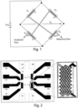
- TCD a typical arrangement of a TCD suited for environmental analysis by means of GC techniques is reported in figure 1 .
- the TCD is formed by two couples of resistors, put in a Wheatstone bridge configuration: the pure carrier gas (reference) flow enters resistors R 1 and R 4 , while the flow from analytical column (carrier gas + eluted sample component) enters resistors R 2 and R 3 .
- thermal conductivity of the analytical flow differs from thermal conductivity of the carrier gas that enters R 1 and R 4 ; for this reason, the temperature of R 2 and R 3 will differ from the temperature of R 1 and R 4 and, since a resistance is a temperature-dependent device, eq. (1) is not satisfied and a nonzero voltage measurement is obtained (V B ⁇ 0 V), revealing the presence of the sample substance.
- Patent document US 2010/0242573 A1 discloses a detector according to preamble of claim 1.
- the arrangement herein disclosed in detail is such that, like patent TW494233 , in each cell the two resistors are fabricated on two membranes located in two near, but different positions in the flow of the gas (see e.g. Fig. 5 reported on the patent document US 2010/0242573 A1 ), and therefore artifacts are introduced in the measurement. Indeed, due to this very geometrical construction, artifacts are introduced (see Fig. 7 ):
- TCD Silicon micro-machined thermal conductivity detector
- GC Gas-Chromatographic
- TCD thermal conductivity detector
- GC gas-chromatographic
- the two resistors of each cell are substantially located in the same position along the gas flow, so that they are subjected to the same mechanism of thermal exchange with the accuracy of the detector, and ii) the capability to detect all the gas peaks out-coming from fast GC column without artifacts is improved.
- said first and fourth resistors are fabricated on a same suspended membrane and said second and third resistors are fabricated on a same different suspended membranes.
- said first and fourth resistors are defined over a same suspended dielectric membrane and interdigitated, and said second and third resistors are defined over a same suspended dielectric membrane and interdigitated.
- said first and fourth resistors are overlapped on two different metallization layers and electrically insulated by means of a passivation layer and said second and third resistors are overlapped on two different metallization layers and electrically insulated by means of a passivation layer.
- the present invention further relates to a method of fast gas-chromatographic analysis of a gas sample composed by a carrier gas mixed with an eluted sample component, characterized in that the detector of the invention is used and in that the following steps are executed:
- TCD Thermal Conductivity Detector
- the two resistors of the considered cell are subject to the same mechanism of thermal exchange with the incoming flow, both spatially and temporally, so increasing the sensitivity and accuracy of the detector.
- L T in a TCD where the resistor segments are positioned sequentially along the sample flow direction, the length L T is the sum of the length of both resistors (L R + L R ), plus the void distance (L V ) between the two resistors.
- L T is at most L T + L R /10 (see Fig. 10 ) .
- the length of the resistor segments L T generating the TCD response should be comparable or smaller than the length of the peak inside the TCD detector chamber, L P .
- L P PD ⁇ FV ⁇ CCS TCS being:
- L P is very small compared to a standard GC peak, and therefore a TCD with a L R shorter than 858 microns, as proposed in this invention, is required to acquire the signal without artifacts.
- the proposed solution ensures a reduction of the overall dimensions of the device and, as a consequence, of dead volumes, which are one of the most common sources of extra-column band broadening that affect the fast GC analysis of gaseous compounds [11] .
- the invention micro-fabricated TCD is formed by two couples of nominally equal platinum resistors, put in a Wheatstone bridge configuration, defined over suspended dielectric membranes obtained through silicon micromachining techniques.
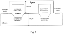
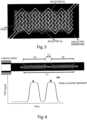
- the silicon chip containing the suspended structures is surrounded by a pyrex cover forming two ultra-low-volume micro-chambers (the reference channel and the analytical channel) where the device is encapsulated: a picture of the device cross-section is illustrated in figure 2 .
- each resistor of the bridge is defined over a single suspended membrane, as illustrated in figure 3 taken from the patent TW494233 by Hsien Wen Ko and Li Hsu (2002).
- the novel aspect of the proposed TCD is represented by the fact that the device layout has been designed so that BOTH resistors of a single channel are defined over a SINGLE suspended membrane, made e.g. of a stress-compensated SiO2 - Si3N4 - SiO2 stack.
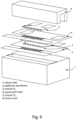
- both the two resistors of the reference channel and the two resistors of the analytical channel are interdigitated and defined by using a single metallization layer (e.g. platinum), while in a second embodiment (see Fig. 9 ) both the two resistors of the reference channel and the two resistors of the analytical channel are defined by using two overlapped metallization layers (e.g. platinum) electrically insulated by means of a passivation layer.
- a single metallization layer e.g. platinum
- both the two resistors of the reference channel and the two resistors of the analytical channel are defined by using two overlapped metallization layers (e.g. platinum) electrically insulated by means of a passivation layer.
- the references are (only the analytical channel is illustrated):
- each pair of resistors (L T ) as taken along the gas flow does not exceed 10% of the length of a single resistor (L R ), so that they are substantially located in the same position along the gas flow.
- the configuration optimized by reduced length of the area occupied by the resistors contributes in eliminating artifacts induced by short gas packet, characteristic of the fast GC.
- Locating the two resistors extremely close to each other makes them subjected to the same mechanism of thermal exchange with the incoming flow, both spatially and temporally, increasing the sensitivity and accuracy of the detector.
- the proposed configuration is characterized by a reduction of the overall dimensions with respect to the solution with a single resistor over a single membrane: this fact is of great advantage especially for GC applications where rapid analysis cycles are required (FAST-GC applications), since one of the mandatory issues that must be satisfied for such analysis relies on the reduction of dead volumes as much as possible.
- Fig. 9 shows the disassembled view of the most compact version of the TCD innovative layout: this solution prefigures the deposition, over the single suspended membrane, of a first metallization layer (resistor R 2 ) followed by a passivation layer (Low Thermal Oxide, thickness ⁇ 1 ⁇ m) characterized by the presence of two via holes to permit the electrical connection with the bonding pads.
- a first metallization layer resistor R 2
- a passivation layer Low Thermal Oxide, thickness ⁇ 1 ⁇ m
- the presence of the passivation layer ensures the electrical insulation between resistor R 2 and the second metallization layer corresponding to resistor R 3 , thus avoiding any shortcut between the two resistors of the single branch.
- TCD time-Gas Chromatography
- the first case refers to the "state-of-the-art" of conventional GC, where the innovation of the proposed patent is not strictly necessary. Characteristics of the column:
- the second case refers to the more recent FAST-GC applications, and shows the problem which needs to be addressed.
- the resistors of a micro-machined TCD are preferably realized in a material with the following features:
- the TCR complying with the first requirement could be both a metal (positive TCR) and a semiconductor (negative TCR).
- the preferred used gases are helium and Hydrogen since:
Landscapes
- Chemical & Material Sciences (AREA)
- Chemical Kinetics & Catalysis (AREA)
- Electrochemistry (AREA)
- Physics & Mathematics (AREA)
- Health & Medical Sciences (AREA)
- Life Sciences & Earth Sciences (AREA)
- Analytical Chemistry (AREA)
- Biochemistry (AREA)
- General Health & Medical Sciences (AREA)
- General Physics & Mathematics (AREA)
- Immunology (AREA)
- Pathology (AREA)
- Investigating Or Analyzing Materials By The Use Of Electric Means (AREA)
Description
- The present invention concerns a thermal conductivity detector (TCD) for fast gas-chromatographic (GC) applications.
- More in detail, the present invention concerns a new Thermal Conductivity Detector (TCD) specifically suited for fast Gas Chromatographic (GC) applications. In the TCD of the invention, micro-electromechanical processing technique is used to fabricate a miniaturized device, which consists of two couples of platinum resistors put in a Wheatstone bridge configuration and suspended upon dielectric membranes at the centre of two flowing channels (reference channel and analytical channel). The novel aspect of the proposed layout design consists in locating each couple of resistors over a single dielectric membrane, in order to minimize the area occupied by the couple of resistors as a function of the gas packet length. In fact, with respect to the standard GC, the fast GC column produces shorter gas packet lengths and decreases the time between two peaks of different gas species. The proposed layout design for the innovative TCD reduces the length of the channel, so improving the capability to detect all the gas peaks out-coming from fast GC column without artifacts. Taking advantage of the proposed layout, unwanted phenomena like band broadening with overlapping of different gas peaks are avoided by using length of the area occupied by the resistors shorter than each single gas packet length: for this reason, the proposed TCD layout makes the invention device suitable for applications like fast-GC.
- Moreover, the proposed solution locates the two resistors extremely close each other, so that they are subjected to the same mechanism of thermal exchange with the incoming flow (both spatially and temporally), increasing the sensitivity and accuracy of the detector.
- A detector is an essential part of a gas chromatographic system. Of the various detectors that have been developed for GC instruments, the thermal conductivity detector (TCD) is probably the first and the mostly widely used detection system in general gas analysis and in environmental testing. A TCD operates on relative changes in the thermal conductivity of gas flowing through separate sample and reference cells of the TCD. A conventional TCD typically contains, in the sample and reference cells, pairs of electrically heated filaments whose temperature at constant electrical power depends upon the thermal conductivity of the surrounding gas. However, using the photolithography technique and chemical or physical deposition processes developed for fabricating microelectronics devices, TCDs which are several orders of magnitude smaller than conventional hot-wire or thermistor-bead TCDs have been developed in order to fabricate miniature GC system.
- Although the TCD is not as sensitive as solute property detectors such as the flame ionization detector (FID), it is particularly suited for miniaturization. TCDs are concentration sensitive devices while detectors of higher sensitivities are mass sensitive, like the ionization detectors. As the detector size is reduced, the detector volume decreases, but the gas concentration is not greatly affected. Thus TCDs are at a large advantage in a miniature GC system compared to other types of GC detectors.
- Extensive studies of conventional TCDs have been carried out and published in various books (e.g. [1]) and technical journals (e.g. [2-5]). On the other hand, few research results on micro TCDs (pTCD) fabricated using the lithography technique were published [6-10] despite the fact that silicon-based µTCDs have become commercially available since several years.
- The TCD is identified as a physical detector, since it responds to some difference in the thermal conductivity (a physical property) of a "carrier gas" caused by the presence of the eluted components.
- The most common example of TCD is represented by a wire filament heated by the electrical current flowing through it: using a wire with a temperature dependent resistance, the temperature of the wire can be measured according to the well known relation:

- If the filament is surrounded by a reference gas, small changes in gas thermal conductivity due to the presence of sample components (different from the reference gas) cause variations in temperature T, that can be detected by the change in wire filament resistance.
- The TCD is commonly operated using helium or hydrogen as the carrier gas, since the thermal conductivity of these gases (respectively 0.142 W/m·K and 0.160 W/m·K @ 298K) is higher than that of all the typical solutes.
- The previously described working principle of the TCD is clearly suitable for implementing a differential measurement scheme: the presence of the sample component, in fact, can be better revealed by comparing the thermal conductivity of the pure carrier gas with the thermal conductivity of the mixture represented by the carrier gas in addition with the analyte.
- A typical arrangement of a TCD suited for environmental analysis by means of GC techniques is reported in
figure 1 . The TCD is formed by two couples of resistors, put in a Wheatstone bridge configuration: the pure carrier gas (reference) flow enters resistors R1 and R4, while the flow from analytical column (carrier gas + eluted sample component) enters resistors R2 and R3. - The four resistor are designed such that, in absence of sample eluted from the column, the Wheatstone bridge results balanced, that is:

- As a substance elutes from the column and enters R2 and R3 (together with the carrier gas), thermal conductivity of the analytical flow differs from thermal conductivity of the carrier gas that enters R1 and R4; for this reason, the temperature of R2 and R3 will differ from the temperature of R1 and R4 and, since a resistance is a temperature-dependent device, eq. (1) is not satisfied and a nonzero voltage measurement is obtained (VB ≠ 0 V), revealing the presence of the sample substance.
- Here we focus on micro-fabricated TCD detectors with one sample and one reference cell made each one of a pair of resistors fabricated on suspended membranes. In the sample cell the pair of resistors is located in the flow of the carrier gas containing solutes coming from the analytical column, while in the reference cell the pair of resistors is located in the flow of the carrier gas. As carrier gas containing solutes passes through the sample cell, a change of the resistance occurs due to the change of the temperature of the resistor. A comparison is made with the resistances of the reference cell by using a Wheatstone bridge circuit. This approach is proposed in the patent
TW494233 Fig. 2 ). - Patent document
US 2010/0242573 A1 discloses a detector according to preamble ofclaim 1. However, the arrangement herein disclosed in detail is such that, like patentTW494233 Fig. 5 reported on the patent documentUS 2010/0242573 A1 ), and therefore artifacts are introduced in the measurement. Indeed, due to this very geometrical construction, artifacts are introduced (seeFig. 7 ): - Peaks are detected two times;
- Peaks are partially superimposed.
- It is the object of the present invention to provide a Silicon micro-machined thermal conductivity detector (TCD), in particular for fast Gas-Chromatographic (GC) applications, which solves the problems and overcomes the drawbacks of the prior art.
- The present invention is defined in the claims and provide a thermal conductivity detector (TCD) for fast gas-chromatographic (GC) analysis of a gas sample composed by a carrier gas mixed with an eluted sample component, comprising:
- A reference cell through which said carrier gas flows along a reference cell direction, comprising:
- o a first resistor occupying a first resistor segment along said reference cell direction, the first resistor being sensitive to temperature and having resistance value R1,
- o a fourth resistor occupying a fourth resistor segment along said reference cell direction, the fourth resistor being sensitive to temperature and having resistance value R4,
- A sample cell through which said carrier gas flows along a sample cell direction, comprising:
- o a second resistor occupying a second resistor segment along said sample cell direction, the second resistor being sensitive to temperature and having resistance value R2,
- o a third resistor occupying a third resistor segment along said sample cell direction, the third resistor being sensitive to temperature and having resistance value R3,
the position of said first resistor segment (R1) along said reference cell direction substantially coincides with the position of said fourth resistor segment (R4) along said reference cell direction;- the position of said second resistor segment along said reference cell direction substantially coincides with the position of said third resistor segment along said reference cell direction;
- the positions of said first and fourth resistor segments along said reference cell direction is such that their total length taken up along said reference cell direction exceeds at most for the 10% the length;
- of the single first or fourth resistor segments; and
- the positions of said second and third resistor segments along said sample cell direction is such that their total length taken up along said sample cell direction exceeds at most for the 10% the length of the single second or third resistor segments.
- In such geometrical arrangement, i) the two resistors of each cell are substantially located in the same position along the gas flow, so that they are subjected to the same mechanism of thermal exchange with the accuracy of the detector, and ii) the capability to detect all the gas peaks out-coming from fast GC column without artifacts is improved.
- Preferably according to the invention, said first and fourth resistors are fabricated on a same suspended membrane and said second and third resistors are fabricated on a same different suspended membranes.
- Preferably according to the invention, said first and fourth resistors are defined over a same suspended dielectric membrane and interdigitated, and said second and third resistors are defined over a same suspended dielectric membrane and interdigitated.
- Preferably according to the invention, said first and fourth resistors are overlapped on two different metallization layers and electrically insulated by means of a passivation layer and said second and third resistors are overlapped on two different metallization layers and electrically insulated by means of a passivation layer.
- The present invention further relates to a method of fast gas-chromatographic analysis of a gas sample composed by a carrier gas mixed with an eluted sample component, characterized in that the detector of the invention is used and in that the following steps are executed:
- A. selecting the gas sample;
- B. providing the detector of the invention with first, second, third, fourth resistor segments such that the total length of the first and fourth segment along said reference cell direction, and the total length of the second and third segment along said sample cell direction, are smaller than the length of a gas packet of the gas sample;
- C. sending said gas sample in the detector;
- D. measuring thermal conductivity of the gas sample.
- The invention will be now described by way of illustration but not by way of limitation, with particular reference to the figures of the annexed drawings, wherein:
-
figure 1 shows a typical prior art arrangement of a TCD suited for environmental analysis by means of GC techniques; -
figure 2 shows a silicon chip containing the suspended structures, surrounded by a pyrex cover forming two ultra-low-volume micro-chambers (the reference channel and the analytical channel) where the device is encapsulated, for a TCD device; -
figure 3 shows a commonly used miniaturized TCD according to patentTW494233 by Hsien Wen Ko and Li Hsu (2002 -
figure 4 shows a layout of an embodiment of the TCD according to the present invention; -
figure 5 shows an optical micrograph of the micro-fabricated element located in one of the channels of the invention device offigure 4 ; -
figure 6 shows the effect of a standard GC column (i.e. not fast GC) on conventional prior art TCD; -
figure 7 shows the effect of a FAST-GC column on conventional prior art TCD, wherein artifacts appear; -
figure 8 shows the effect of a FAST-GC column on the device according to the invention, wherein artifacts are eliminated; -
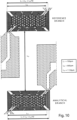
figure 9 shows the most compact version of the proposed solution, wherein the two metallization layers corresponding to the two resistors of a single branch of the TCD are overlapped and electrically insulated by means of a passivation layer; and -
Fig. 10 shows the mutual position of each pair of resistors in one embodiment of the TCD according to the present invention, together with the main geometrical features. - Taking into account the electrical configuration of the four resistances in the Wheatstone bridge circuit, such a geometrical arrangement is improved according to the invention by locating the two resistors of each cell in the same position in the gas flow. In particular, the innovation provided by the layout design of the developed Thermal Conductivity Detector (TCD) consists in the definition, both for the reference channel and the analytical channel, of a couple of platinum resistors over a single suspended dielectric membrane. In this way, the area occupied by each couple of resistors as a function of the gas packet length is optimized and, as a consequence, the sensitivity and the accuracy of the detector are increased.
- Moreover, the two resistors of the considered cell are subject to the same mechanism of thermal exchange with the incoming flow, both spatially and temporally, so increasing the sensitivity and accuracy of the detector.
- In order to show that, consider the length of the area occupied by the resistors generating the TCD response, LT: in a TCD where the resistor segments are positioned sequentially along the sample flow direction, the length LT is the sum of the length of both resistors (LR + LR), plus the void distance (LV) between the two resistors.
- In the TCD of the present invention, where the area occupied by both resistor segments coincide, LT is at most LT + LR/10 (see
Fig. 10 ) . - For a GC peak to be detected without artifacts, as a general rule, the length of the resistor segments LT generating the TCD response should be comparable or smaller than the length of the peak inside the TCD detector chamber, LP.
- The parameter LP is a function of the injection time and of the geometrical features of the GC column, as explained by the formula:

- PD the peak duration (or injection time) (sec)
- FV the flow velocity in column (m/sec)
- CCS the column cross section (m2)
- TCS the TCD chamber cross section (m2).
- In the following, three cases of ratios between LR and LP are reported together with the expected analysis quality:
- ▪ LT/LP > 1: artifacts as described in
fig. 7 . - ▪ LT/LP ≤ 1: no artifacts, and a very high temporal resolution is possible (see
Fig. 8 ). - In the following, some typical figures of STANDARD GC peaks vs. FAST-GC peaks are reported, as they are eluted into a couple of TCD sensor chambers (reference branch and analytical branch) of 0.2mm x 0.2mm cross section.
- Case A) Typical peak of a standard GC analysis:
- Optimal linear flow velocity in column: 350 mm/s
- Column inner diameter: 350 microns
- Column cross section 0.096 mm2
- Typical peak duration: 1 second
- Peak length inside the TCD detector chamber LP:

- Case B) Typical FAST-GC peak:
- Optimal linear flow velocity in column: 350 mm/s
- Column inner diameter: 50 microns
- Column cross section 0.00196 mm2
- Typical peak duration: 0.05 seconds
- Peak length inside the TCD detector chamber LP:

- As can be easily disclosed, in the case of a FAST-GC peak, LP is very small compared to a standard GC peak, and therefore a TCD with a LR shorter than 858 microns, as proposed in this invention, is required to acquire the signal without artifacts.
- Moreover, the proposed solution ensures a reduction of the overall dimensions of the device and, as a consequence, of dead volumes, which are one of the most common sources of extra-column band broadening that affect the fast GC analysis of gaseous compounds [11] .
- In particular, the invention micro-fabricated TCD is formed by two couples of nominally equal platinum resistors, put in a Wheatstone bridge configuration, defined over suspended dielectric membranes obtained through silicon micromachining techniques. The silicon chip containing the suspended structures is surrounded by a pyrex cover forming two ultra-low-volume micro-chambers (the reference channel and the analytical channel) where the device is encapsulated: a picture of the device cross-section is illustrated in
figure 2 . In the most commonly used miniaturized TCDs, each resistor of the bridge is defined over a single suspended membrane, as illustrated infigure 3 taken from the patentTW494233 - On the contrary, the novel aspect of the proposed TCD is represented by the fact that the device layout has been designed so that BOTH resistors of a single channel are defined over a SINGLE suspended membrane, made e.g. of a stress-compensated SiO2 - Si3N4 - SiO2 stack.
- On the contrary, the novel aspect of the proposed TCD is
- represented by the fact that the device layout has been designed so that
- 5 BOTH resistors of a single channel are defined over a SINGLE suspended
- membrane, made e.g. of a stress-compensated SiO2 - Si3N4 - SiO2
- stack.
- In order to achieve the target, two different solutions were adopted: in a first embodiment (see
Figs. 4 ,5 ,10 ) both the two resistors of the reference channel and the two resistors of the analytical channel are interdigitated and defined by using a single metallization layer (e.g. platinum), while in a second embodiment (seeFig. 9 ) both the two resistors of the reference channel and the two resistors of the analytical channel are defined by using two overlapped metallization layers (e.g. platinum) electrically insulated by means of a passivation layer. Infigure 9 the references are (only the analytical channel is illustrated): - 1 - Silicon Chip
- 2 - Dielectric membrane
- 3 - Resistor R2 (Resistor area = 600umX170um) 20 4 - Passivation Layer
- 5 - Resistor R3 (Resistor Area = 600umX170um)
- 6 - Pyrex covering.
- In any case, the length of each pair of resistors (LT) as taken along the gas flow does not exceed 10% of the length of a single resistor (LR), so that they are substantially located in the same position along the gas flow.
- The configuration optimized by reduced length of the area occupied by the resistors contributes in eliminating artifacts induced by short gas packet, characteristic of the fast GC.
- Locating the two resistors extremely close to each other makes them subjected to the same mechanism of thermal exchange with the incoming flow, both spatially and temporally, increasing the sensitivity and accuracy of the detector.
- Moreover, the proposed configuration is characterized by a reduction of the overall dimensions with respect to the solution with a single resistor over a single membrane: this fact is of great advantage especially for GC applications where rapid analysis cycles are required (FAST-GC applications), since one of the mandatory issues that must be satisfied for such analysis relies on the reduction of dead volumes as much as possible.
- On this purpose,
Fig. 9 shows the disassembled view of the most compact version of the TCD innovative layout: this solution prefigures the deposition, over the single suspended membrane, of a first metallization layer (resistor R2) followed by a passivation layer (Low Thermal Oxide, thickness ~ 1 µm) characterized by the presence of two via holes to permit the electrical connection with the bonding pads. - The presence of the passivation layer ensures the electrical insulation between resistor R2 and the second metallization layer corresponding to resistor R3, thus avoiding any shortcut between the two resistors of the single branch.
- This configuration allows a maximal reduction of the overall dimensions of the device, since the two interdigitated resistors (defined on the same metallization layer) are replaced by two superimposed resistors (defined on two different metallization layers), so that the lateral distance between the resistors is equal to zero (LT = LR).
- The different requirement for normal and fast GC are given in the following table.
Conventional GC: FAST-GC: column length: 10 - 60 m column length: 2 - 10 m column ID: 150 - 530 um column ID: 50 - 100 um column flow: 1 - 6 sccm column flow: 0.1 - 0.5 sccm analysis cycle: 10 - 30 min analysis cycle: 1 - 5 min - A great advantage of the proposed TCD consists in the use of silicon micromachining techniques to fabricate, at wafer level, a miniaturized device characterized by extremely small dimensions and, as a consequence, extremely reduced dead volumes: this is an important issue for applications like fast-Gas Chromatography (fast-GC), where low flow-rates are required.
- To illustrate this in greater detail, three examples are reported in
figures 6-8 : - "Standard" GC column (= not FAST) on conventional TCD (
figure 6 ); - FAST-GC column on conventional TCD: artifacts (
figure 7 ); - FAST-GC column on the device according to the invention (
figure 8 ). - The first case refers to the "state-of-the-art" of conventional GC, where the innovation of the proposed patent is not strictly necessary.
Characteristics of the column: - - The "standard" GC column works with a rather high flow rates
- - The peaks have a relatively long duration.
- - The temporal separation between two peaks is relatively large.
- In this case the peaks are correctly separated without artifacts.
- The second case refers to the more recent FAST-GC applications, and shows the problem which needs to be addressed.
- Characteristics of the column:
- The FAST-GC column works with very low flow rates.
- The peaks have a very short duration.
- The temporal separation between two peaks is low.
- A prior art detector with a spatial separation between the resistors is not suitable to acquire the chromatogram. Indeed, due to this very geometrical construction, artifacts are introduced:
- Peaks are detected two times;
- Peaks are partially superimposed.
- In the third case, with reference to
figure 8 , a FAST-GC column on invention TCD is used. Characteristics of the column: - The FAST-GC column works with very low flow rates.
- The peaks have a very short duration.
- The temporal separation between two peaks is low.
- The peaks in this case are correctly separated without any artifacts.
- Moreover, the reduction of overall dimensions allows very low power consumptions needed to operate the device.
- The resistors of a micro-machined TCD are preferably realized in a material with the following features:
- 1. TCR module as large as possible;
- 2. good resistance to temperature during use, up to and beyond 400°C: the material should not change the electric and mechanical properties at these temperatures;
- 3. no irreversible chemical interaction with the sample to be analyzed (in other words "chemically inert")
- 4. possibility to be deposed and defined with microelectronics processes;
- The TCR complying with the first requirement could be both a metal (positive TCR) and a semiconductor (negative TCR).
- Many of the typical metals used in microelectronics (Al, Au, Cu) do not satisfy
points - The material best satisfying all the four points has been individuated in the Pt.
- The preferred used gases are helium and Hydrogen since:
- both ones are optimal carrier gases typically used in GC, because they do not damage the stationary phase of the column;
- among the carrier gases typically used in GC (helium, Hydrogen and Nitrogen), only Helium and Hydrogen have a very high thermal conductivity and very different from the thermal conductivities of the typical samples to be analyzed, what maximizes the response of the del TCD.
-
- [1] H.A. Daynes, "Gas Analysis by Measurement of Thermal Conductivity", Cambridge University Press, Cambridge, Great Britain, pp. 1-302 (1933).
- [2] W.A. Wiseman, "Katharometer behavior", Ann. N.Y. Acad. Sci. 72, pp. 685-697 (1959).
- [3] D.M. Rosie, "Quantization of thermal conductivity detectors", J.Chromatogr. Sci. 11, pp. 237-250 (1973).
- [4] J. Sevcik, "Detectors in gas chromatography", J. Chromatogr. ).
- [5] Y. Huang, H.H. Bau, "The effects of forced convection on the power dissipation of constant-temperature thermal conductivity sensors", ASME J. Heat Transfer 119, pp. 30-37 (1997).
- [6] S.C. Terry, J.H. Jerman, J.B. Angell, "A gas chromatographic air analyzer fabricated on a silicon wafer", IEEE Trans. Electr. Devices ED-26 (12), pp. 1880-1886 (1979).
- [7] Wu Y E, Chen K, Chen C W and Hsu K H, "Fabrication and characterization of thermal conductivity detectors (TCDs) of different flow channel and heater designs", Sensors & Actuators A 100, pp. 37-45 (2002).
- [8] Cruz D, Chang J P, Showalter S K, Gelbrad F, Manginell R P and Blain M G, "Microfabricated thermal conductivity detector for the micro-ChemLab", Sensors & Actuators B 121, pp. 414 - 422 (2007).
- [9] J. A. Dziuban, J. Mroz, M. Szczygielska, A. Gorecka-Drzazga, R. Walczak, W. Bula, D. Zalewzki, L. Nieradko, J. Lysko, J. Koszur, P. Kowalski, "Portable gas chromatograph with integrated components", Sensors & Actuators A 115, pp. 318-330 (2004).
- [10] B. C. Kaanta, H. Chen, X. Zhang, "Effect of forced convection on thermal distribution in micro thermal conductivity detectors", J. Micromech. ).
- [11] V. R. Reid, R. E. Synovec, "High-speed gas chromatography: The importance of instrumentation optimization and the elimination of extra-column band broadening", Talanta 76, pp. 703-717 (2008).
Claims (4)
- Thermal conductivity detector (TCD) for fast gas-chromatographic (GC) analysis of a gas sample composed by a carrier gas mixed with an eluted sample component, comprising:- A reference cell through which said carrier gas flows along a reference cell direction, comprising:o a first resistor (R1) occupying a first resistor segment along said reference cell direction, the first resistor being sensitive to temperature and having resistance value R1,o a fourth resistor (R4) occupying a fourth resistor segment along said reference cell direction, the fourth resistor being sensitive to temperature and having resistance value R4,- A sample cell through which said carrier gas flows along a sample cell direction, comprising:o a second resistor (R2) occupying a second resistor segment along said sample cell direction, the second resistor being sensitive to temperature and having resistance value R2,o a third resistor (R3) occupying a third resistor segment along said sample cell direction, the third resistor being sensitive to temperature and having resistance value R3,the first, second, third and fourth resistors being disposed together in a Wheatstone bridge configuration, such that, in absence of said sample eluted, the Wheatstone bridge results balanced, that is R1·R4 = R2·R3, the thermal conductivity detector being characterised in that:- the position of said first resistor segment (R1) along said reference cell direction substantially coincides with the position of said fourth resistor segment (R4) along said reference cell direction;- the position of said second resistor segment along said reference cell direction substantially coincides with the position of said third resistor segment along said reference cell direction;- the positions of said first and fourth resistor segments along said reference cell direction is such that their total length taken up along said reference cell direction exceeds at most for the 10% the length of the single first or fourth resistor segments; and- the positions of said second and third resistor segments along said sample cell direction is such that their total length taken up along said sample cell direction exceeds at most for the 10% the length of the single second or third resistor segments.
- Detector according to claim 1, characterised in that said first and fourth resistors (R1,R4) are defined over a same suspended dielectric membrane and interdigitated, and said second and third resistors (R2,R3) are defined over a same suspended dielectric membrane and interdigitated.
- Detector according to claim 1, characterised in that said first and fourth resistors (R1,R4) are overlapped on two different metallization layers and electrically insulated by means of a passivation layer and said second and third resistors (R2,R3) are overlapped on two different metallization layers and electrically insulated by means of a passivation layer.
- Method of fast gas-chromatographic (GC) analysis of a gas sample composed by a carrier gas mixed with an eluted sample component, characterized in that the detector of any one claim 1 to 3 is used and in that the following steps are executed:A. selecting the gas sample;B. providing the detector of the invention with first, second, third, fourth resistor (R1, R2, R3, R4) segments such that the total length of the first and fourth segment along said reference cell direction, and the total length of the second and third segment along said sample cell direction, are smaller than the length of a gas packet of the gas sample;C. sending said gas sample in the detector;D. measuring thermal conductivity of the gas sample.
Applications Claiming Priority (2)
| Application Number | Priority Date | Filing Date | Title |
|---|---|---|---|
| IT000311A ITRM20120311A1 (en) | 2012-07-04 | 2012-07-04 | THERMAL CONDUCTIVITY DETECTOR (TCD) FOR FAST GAS-CHROMATOGRAPHY APPLICATIONS (GC). |
| PCT/IT2013/000178 WO2014006648A1 (en) | 2012-07-04 | 2013-06-27 | Thermal conductivity detector (tcd) for applications in fast gas- chromatographic (gc) |
Publications (3)
| Publication Number | Publication Date |
|---|---|
| EP2870465A1 EP2870465A1 (en) | 2015-05-13 |
| EP2870465C0 EP2870465C0 (en) | 2023-12-06 |
| EP2870465B1 true EP2870465B1 (en) | 2023-12-06 |
Family
ID=46800293
Family Applications (1)
| Application Number | Title | Priority Date | Filing Date |
|---|---|---|---|
| EP13756701.2A Active EP2870465B1 (en) | 2012-07-04 | 2013-06-27 | Thermal conductivity detector (tcd) for applications in fast gas-chromatography (gc) |
Country Status (3)
| Country | Link |
|---|---|
| EP (1) | EP2870465B1 (en) |
| IT (1) | ITRM20120311A1 (en) |
| WO (1) | WO2014006648A1 (en) |
Families Citing this family (12)
| Publication number | Priority date | Publication date | Assignee | Title |
|---|---|---|---|---|
| DE102014016712B4 (en) * | 2014-11-13 | 2022-12-01 | Dräger Safety AG & Co. KGaA | Transportable chip measurement system and method for operating a transportable chip measurement system |
| GB201421102D0 (en) | 2014-11-27 | 2015-01-14 | Cambridge Entpr Ltd | Thermal conductivity sensing device, methods for operation and uses of the same |
| CN105891394B (en) * | 2014-12-09 | 2018-05-29 | 山东鲁南瑞虹化工仪器有限公司 | A kind of thermal conductivity cell detector |
| CN108700533B (en) * | 2016-03-07 | 2021-04-20 | 株式会社岛津制作所 | Thermal conductivity detector |
| DE102016205776A1 (en) * | 2016-04-07 | 2017-10-12 | Robert Bosch Gmbh | Calorimetric determination of a gas concentration |
| FR3053793A1 (en) * | 2017-01-19 | 2018-01-12 | Commissariat Energie Atomique | GAS ANALYSIS DEVICE BY CATHAROMETRIC DETECTION |
| JP7040092B2 (en) * | 2018-02-13 | 2022-03-23 | 横河電機株式会社 | Detector for gas chromatograph |
| DE102020214581A1 (en) * | 2020-11-19 | 2022-05-19 | Robert Bosch Gesellschaft mit beschränkter Haftung | Sensor for detecting at least one property of a fluid medium in at least one measuring space |
| JP7578218B2 (en) * | 2021-03-11 | 2024-11-06 | Mmiセミコンダクター株式会社 | Thermal Sensor Chip |
| US11867648B2 (en) * | 2021-06-22 | 2024-01-09 | Flusso Limited | Thermal fluid sensor with encapsulated fluid region |
| CN114839307B (en) * | 2022-04-26 | 2024-05-03 | 华中农业大学 | Gas-sensitive detection chip based on thermal conductivity cell array and application of gas-sensitive detection chip in food freshness detection |
| CN117783401B (en) * | 2023-12-26 | 2025-06-27 | 中国科学院上海微系统与信息技术研究所 | Single-channel micro-thermal conductivity detector and preparation method thereof |
Family Cites Families (5)
| Publication number | Priority date | Publication date | Assignee | Title |
|---|---|---|---|---|
| US6502983B2 (en) * | 1999-03-30 | 2003-01-07 | The Regents Of The University Of California | Micro-machined thermo-conductivity detector |
| TW494233B (en) | 2000-02-25 | 2002-07-11 | Chung Shan Inst Of Science | Thermal conductivity detector |
| GR1004040B (en) * | 2001-07-31 | 2002-10-31 | Method for the fabrication of suspended porous silicon microstructures and application in gas sensors | |
| US7021821B2 (en) * | 2004-05-28 | 2006-04-04 | Honeywell International Inc. | Differential thermal sensors |
| US8302459B2 (en) * | 2009-03-27 | 2012-11-06 | Horiba, Ltd. | Thermal conductivity sensor |
-
2012
- 2012-07-04 IT IT000311A patent/ITRM20120311A1/en unknown
-
2013
- 2013-06-27 WO PCT/IT2013/000178 patent/WO2014006648A1/en not_active Ceased
- 2013-06-27 EP EP13756701.2A patent/EP2870465B1/en active Active
Also Published As
| Publication number | Publication date |
|---|---|
| WO2014006648A1 (en) | 2014-01-09 |
| EP2870465C0 (en) | 2023-12-06 |
| EP2870465A1 (en) | 2015-05-13 |
| ITRM20120311A1 (en) | 2014-01-05 |
Similar Documents
| Publication | Publication Date | Title |
|---|---|---|
| WO2014006648A1 (en) | Thermal conductivity detector (tcd) for applications in fast gas- chromatographic (gc) | |
| EP3523646B1 (en) | Multi-channel multi-dimensional comprehensive gas chromatography | |
| EP3292401B1 (en) | Microfluidic photoionization detector | |
| Akbar et al. | GC-on-chip: integrated column and photoionization detector | |
| Tian et al. | Microfabricated preconcentrator-focuser for a microscale gas chromatograph | |
| US9128028B2 (en) | Thermal conductivity detectors | |
| EP1994405B1 (en) | A three-wafer channel structure for a fluid analyzer | |
| US20040255643A1 (en) | High-performance separation microcolumn assembly and method of making same | |
| WO2005068996A2 (en) | Phased micro analyzer iv | |
| Lee et al. | In situ calibration of micro-photoionization detectors in a multi-dimensional micro-gas chromatography system | |
| CA2775583A1 (en) | Micro-thermal conductivity detector, method to fabricate such and chromatography system using such | |
| Gràcia et al. | Sub-ppm gas sensor detection via spiral μ-preconcentrator | |
| EP2706353B1 (en) | Gas chromatograph with thermal conductivity detectors in series | |
| WO2007081416A1 (en) | Ionization-based detection | |
| Lorenzelli et al. | Development of a gas chromatography silicon-based microsystem in clinical diagnostics | |
| WO2000058723A2 (en) | Micro-machined thermal conductivity detector | |
| US9116160B2 (en) | Method and arrangement for gas chromatographic analysis of a gas sample | |
| EP1876453A1 (en) | Integrated chip temperature control | |
| US4067227A (en) | Hydrogen transfer system for gas chromatograph | |
| WO1998015823A1 (en) | Poly-capillary chromatographic column | |
| US10481135B1 (en) | Separation devices and sensors including two dimensional materials that change properties when exposed to components separated from a sample | |
| CN117783401A (en) | Single-channel micro-thermal conductivity detector and preparation method thereof | |
| RU2266534C2 (en) | Thermal conductivity detector for gas chromatography | |
| Han et al. | Micro-fabricated packed metal gas preconcentrator for low detection limit exhaled VOC gas measurements | |
| Jurdit et al. | Investigating the variation of thermal conductivity with temperature to improve a portable gas chromatography (GC) system's specificity |
Legal Events
| Date | Code | Title | Description |
|---|---|---|---|
| PUAI | Public reference made under article 153(3) epc to a published international application that has entered the european phase |
Free format text: ORIGINAL CODE: 0009012 |
|
| 17P | Request for examination filed |
Effective date: 20150128 |
|
| AK | Designated contracting states |
Kind code of ref document: A1 Designated state(s): AL AT BE BG CH CY CZ DE DK EE ES FI FR GB GR HR HU IE IS IT LI LT LU LV MC MK MT NL NO PL PT RO RS SE SI SK SM TR |
|
| AX | Request for extension of the european patent |
Extension state: BA ME |
|
| DAX | Request for extension of the european patent (deleted) | ||
| STAA | Information on the status of an ep patent application or granted ep patent |
Free format text: STATUS: EXAMINATION IS IN PROGRESS |
|
| 17Q | First examination report despatched |
Effective date: 20190612 |
|
| REG | Reference to a national code |
Ref country code: DE Ref legal event code: R079 Free format text: PREVIOUS MAIN CLASS: G01N0025180000 Ipc: G01N0027180000 Ref country code: DE Ref legal event code: R079 Ref document number: 602013085024 Country of ref document: DE Free format text: PREVIOUS MAIN CLASS: G01N0025180000 Ipc: G01N0027180000 |
|
| GRAP | Despatch of communication of intention to grant a patent |
Free format text: ORIGINAL CODE: EPIDOSNIGR1 |
|
| STAA | Information on the status of an ep patent application or granted ep patent |
Free format text: STATUS: GRANT OF PATENT IS INTENDED |
|
| RIC1 | Information provided on ipc code assigned before grant |
Ipc: G01N 30/88 20060101ALN20230406BHEP Ipc: G01N 30/66 20060101ALI20230406BHEP Ipc: G01N 27/18 20060101AFI20230406BHEP |
|
| INTG | Intention to grant announced |
Effective date: 20230424 |
|
| GRAJ | Information related to disapproval of communication of intention to grant by the applicant or resumption of examination proceedings by the epo deleted |
Free format text: ORIGINAL CODE: EPIDOSDIGR1 |
|
| STAA | Information on the status of an ep patent application or granted ep patent |
Free format text: STATUS: EXAMINATION IS IN PROGRESS |
|
| GRAP | Despatch of communication of intention to grant a patent |
Free format text: ORIGINAL CODE: EPIDOSNIGR1 |
|
| STAA | Information on the status of an ep patent application or granted ep patent |
Free format text: STATUS: GRANT OF PATENT IS INTENDED |
|
| INTC | Intention to grant announced (deleted) | ||
| RIC1 | Information provided on ipc code assigned before grant |
Ipc: G01N 30/88 20060101ALN20230718BHEP Ipc: G01N 30/66 20060101ALI20230718BHEP Ipc: G01N 27/18 20060101AFI20230718BHEP |
|
| INTG | Intention to grant announced |
Effective date: 20230801 |
|
| GRAS | Grant fee paid |
Free format text: ORIGINAL CODE: EPIDOSNIGR3 |
|
| GRAJ | Information related to disapproval of communication of intention to grant by the applicant or resumption of examination proceedings by the epo deleted |
Free format text: ORIGINAL CODE: EPIDOSDIGR1 |
|
| GRAL | Information related to payment of fee for publishing/printing deleted |
Free format text: ORIGINAL CODE: EPIDOSDIGR3 |
|
| STAA | Information on the status of an ep patent application or granted ep patent |
Free format text: STATUS: EXAMINATION IS IN PROGRESS |
|
| GRAP | Despatch of communication of intention to grant a patent |
Free format text: ORIGINAL CODE: EPIDOSNIGR1 |
|
| STAA | Information on the status of an ep patent application or granted ep patent |
Free format text: STATUS: GRANT OF PATENT IS INTENDED |
|
| INTC | Intention to grant announced (deleted) | ||
| RIC1 | Information provided on ipc code assigned before grant |
Ipc: G01N 30/88 20060101ALN20230918BHEP Ipc: G01N 30/66 20060101ALI20230918BHEP Ipc: G01N 27/18 20060101AFI20230918BHEP |
|
| INTG | Intention to grant announced |
Effective date: 20231002 |
|
| GRAA | (expected) grant |
Free format text: ORIGINAL CODE: 0009210 |
|
| STAA | Information on the status of an ep patent application or granted ep patent |
Free format text: STATUS: THE PATENT HAS BEEN GRANTED |
|
| AK | Designated contracting states |
Kind code of ref document: B1 Designated state(s): AL AT BE BG CH CY CZ DE DK EE ES FI FR GB GR HR HU IE IS IT LI LT LU LV MC MK MT NL NO PL PT RO RS SE SI SK SM TR |
|
| REG | Reference to a national code |
Ref country code: GB Ref legal event code: FG4D |
|
| REG | Reference to a national code |
Ref country code: CH Ref legal event code: EP |
|
| REG | Reference to a national code |
Ref country code: DE Ref legal event code: R096 Ref document number: 602013085024 Country of ref document: DE |
|
| REG | Reference to a national code |
Ref country code: IE Ref legal event code: FG4D |
|
| U01 | Request for unitary effect filed |
Effective date: 20231206 |
|
| U07 | Unitary effect registered |
Designated state(s): AT BE BG DE DK EE FI FR IT LT LU LV MT NL PT SE SI Effective date: 20231212 |
|
| PG25 | Lapsed in a contracting state [announced via postgrant information from national office to epo] |
Ref country code: GR Free format text: LAPSE BECAUSE OF FAILURE TO SUBMIT A TRANSLATION OF THE DESCRIPTION OR TO PAY THE FEE WITHIN THE PRESCRIBED TIME-LIMIT Effective date: 20240307 |
|
| PG25 | Lapsed in a contracting state [announced via postgrant information from national office to epo] |
Ref country code: ES Free format text: LAPSE BECAUSE OF FAILURE TO SUBMIT A TRANSLATION OF THE DESCRIPTION OR TO PAY THE FEE WITHIN THE PRESCRIBED TIME-LIMIT Effective date: 20231206 |
|
| PG25 | Lapsed in a contracting state [announced via postgrant information from national office to epo] |
Ref country code: GR Free format text: LAPSE BECAUSE OF FAILURE TO SUBMIT A TRANSLATION OF THE DESCRIPTION OR TO PAY THE FEE WITHIN THE PRESCRIBED TIME-LIMIT Effective date: 20240307 Ref country code: ES Free format text: LAPSE BECAUSE OF FAILURE TO SUBMIT A TRANSLATION OF THE DESCRIPTION OR TO PAY THE FEE WITHIN THE PRESCRIBED TIME-LIMIT Effective date: 20231206 |
|
| PG25 | Lapsed in a contracting state [announced via postgrant information from national office to epo] |
Ref country code: RS Free format text: LAPSE BECAUSE OF FAILURE TO SUBMIT A TRANSLATION OF THE DESCRIPTION OR TO PAY THE FEE WITHIN THE PRESCRIBED TIME-LIMIT Effective date: 20231206 Ref country code: NO Free format text: LAPSE BECAUSE OF FAILURE TO SUBMIT A TRANSLATION OF THE DESCRIPTION OR TO PAY THE FEE WITHIN THE PRESCRIBED TIME-LIMIT Effective date: 20240306 Ref country code: HR Free format text: LAPSE BECAUSE OF FAILURE TO SUBMIT A TRANSLATION OF THE DESCRIPTION OR TO PAY THE FEE WITHIN THE PRESCRIBED TIME-LIMIT Effective date: 20231206 |
|
| PG25 | Lapsed in a contracting state [announced via postgrant information from national office to epo] |
Ref country code: IS Free format text: LAPSE BECAUSE OF FAILURE TO SUBMIT A TRANSLATION OF THE DESCRIPTION OR TO PAY THE FEE WITHIN THE PRESCRIBED TIME-LIMIT Effective date: 20240406 |
|
| U1N | Appointed representative for the unitary patent procedure changed after the registration of the unitary effect |
Representative=s name: DALL'OLIO, CHRISTIAN; IT |
|
| PG25 | Lapsed in a contracting state [announced via postgrant information from national office to epo] |
Ref country code: CZ Free format text: LAPSE BECAUSE OF FAILURE TO SUBMIT A TRANSLATION OF THE DESCRIPTION OR TO PAY THE FEE WITHIN THE PRESCRIBED TIME-LIMIT Effective date: 20231206 |
|
| U20 | Renewal fee for the european patent with unitary effect paid |
Year of fee payment: 12 Effective date: 20240619 |
|
| PG25 | Lapsed in a contracting state [announced via postgrant information from national office to epo] |
Ref country code: SK Free format text: LAPSE BECAUSE OF FAILURE TO SUBMIT A TRANSLATION OF THE DESCRIPTION OR TO PAY THE FEE WITHIN THE PRESCRIBED TIME-LIMIT Effective date: 20231206 |
|
| PG25 | Lapsed in a contracting state [announced via postgrant information from national office to epo] |
Ref country code: SM Free format text: LAPSE BECAUSE OF FAILURE TO SUBMIT A TRANSLATION OF THE DESCRIPTION OR TO PAY THE FEE WITHIN THE PRESCRIBED TIME-LIMIT Effective date: 20231206 Ref country code: SK Free format text: LAPSE BECAUSE OF FAILURE TO SUBMIT A TRANSLATION OF THE DESCRIPTION OR TO PAY THE FEE WITHIN THE PRESCRIBED TIME-LIMIT Effective date: 20231206 Ref country code: RO Free format text: LAPSE BECAUSE OF FAILURE TO SUBMIT A TRANSLATION OF THE DESCRIPTION OR TO PAY THE FEE WITHIN THE PRESCRIBED TIME-LIMIT Effective date: 20231206 Ref country code: IS Free format text: LAPSE BECAUSE OF FAILURE TO SUBMIT A TRANSLATION OF THE DESCRIPTION OR TO PAY THE FEE WITHIN THE PRESCRIBED TIME-LIMIT Effective date: 20240406 Ref country code: CZ Free format text: LAPSE BECAUSE OF FAILURE TO SUBMIT A TRANSLATION OF THE DESCRIPTION OR TO PAY THE FEE WITHIN THE PRESCRIBED TIME-LIMIT Effective date: 20231206 |
|
| PG25 | Lapsed in a contracting state [announced via postgrant information from national office to epo] |
Ref country code: PL Free format text: LAPSE BECAUSE OF FAILURE TO SUBMIT A TRANSLATION OF THE DESCRIPTION OR TO PAY THE FEE WITHIN THE PRESCRIBED TIME-LIMIT Effective date: 20231206 |
|
| PG25 | Lapsed in a contracting state [announced via postgrant information from national office to epo] |
Ref country code: PL Free format text: LAPSE BECAUSE OF FAILURE TO SUBMIT A TRANSLATION OF THE DESCRIPTION OR TO PAY THE FEE WITHIN THE PRESCRIBED TIME-LIMIT Effective date: 20231206 |
|
| REG | Reference to a national code |
Ref country code: DE Ref legal event code: R097 Ref document number: 602013085024 Country of ref document: DE |
|
| PLBE | No opposition filed within time limit |
Free format text: ORIGINAL CODE: 0009261 |
|
| STAA | Information on the status of an ep patent application or granted ep patent |
Free format text: STATUS: NO OPPOSITION FILED WITHIN TIME LIMIT |
|
| 26N | No opposition filed |
Effective date: 20240909 |
|
| PG25 | Lapsed in a contracting state [announced via postgrant information from national office to epo] |
Ref country code: MC Free format text: LAPSE BECAUSE OF FAILURE TO SUBMIT A TRANSLATION OF THE DESCRIPTION OR TO PAY THE FEE WITHIN THE PRESCRIBED TIME-LIMIT Effective date: 20231206 |
|
| REG | Reference to a national code |
Ref country code: CH Ref legal event code: PL |
|
| PG25 | Lapsed in a contracting state [announced via postgrant information from national office to epo] |
Ref country code: IE Free format text: LAPSE BECAUSE OF NON-PAYMENT OF DUE FEES Effective date: 20240627 |
|
| PG25 | Lapsed in a contracting state [announced via postgrant information from national office to epo] |
Ref country code: CH Free format text: LAPSE BECAUSE OF NON-PAYMENT OF DUE FEES Effective date: 20240630 |
|
| PGFP | Annual fee paid to national office [announced via postgrant information from national office to epo] |
Ref country code: GB Payment date: 20250617 Year of fee payment: 13 |
|
| U20 | Renewal fee for the european patent with unitary effect paid |
Year of fee payment: 13 Effective date: 20250618 |
|
| PG25 | Lapsed in a contracting state [announced via postgrant information from national office to epo] |
Ref country code: CY Free format text: LAPSE BECAUSE OF FAILURE TO SUBMIT A TRANSLATION OF THE DESCRIPTION OR TO PAY THE FEE WITHIN THE PRESCRIBED TIME-LIMIT; INVALID AB INITIO Effective date: 20130627 |
|
| PG25 | Lapsed in a contracting state [announced via postgrant information from national office to epo] |
Ref country code: HU Free format text: LAPSE BECAUSE OF FAILURE TO SUBMIT A TRANSLATION OF THE DESCRIPTION OR TO PAY THE FEE WITHIN THE PRESCRIBED TIME-LIMIT; INVALID AB INITIO Effective date: 20130627 |