EP2869413A1 - Method of manufacturing spark plug - Google Patents
Method of manufacturing spark plug Download PDFInfo
- Publication number
- EP2869413A1 EP2869413A1 EP20140189873 EP14189873A EP2869413A1 EP 2869413 A1 EP2869413 A1 EP 2869413A1 EP 20140189873 EP20140189873 EP 20140189873 EP 14189873 A EP14189873 A EP 14189873A EP 2869413 A1 EP2869413 A1 EP 2869413A1
- Authority
- EP
- European Patent Office
- Prior art keywords
- insulator
- assembly
- forward end
- metallic shell
- discharge
- Prior art date
- Legal status (The legal status is an assumption and is not a legal conclusion. Google has not performed a legal analysis and makes no representation as to the accuracy of the status listed.)
- Granted
Links
Images


Classifications
-
- H—ELECTRICITY
- H01—ELECTRIC ELEMENTS
- H01T—SPARK GAPS; OVERVOLTAGE ARRESTERS USING SPARK GAPS; SPARKING PLUGS; CORONA DEVICES; GENERATING IONS TO BE INTRODUCED INTO NON-ENCLOSED GASES
- H01T13/00—Sparking plugs
- H01T13/58—Testing
- H01T13/60—Testing of electrical properties
-
- H—ELECTRICITY
- H01—ELECTRIC ELEMENTS
- H01T—SPARK GAPS; OVERVOLTAGE ARRESTERS USING SPARK GAPS; SPARKING PLUGS; CORONA DEVICES; GENERATING IONS TO BE INTRODUCED INTO NON-ENCLOSED GASES
- H01T21/00—Apparatus or processes specially adapted for the manufacture or maintenance of spark gaps or sparking plugs
- H01T21/02—Apparatus or processes specially adapted for the manufacture or maintenance of spark gaps or sparking plugs of sparking plugs
Definitions
- the present invention relates to a method of manufacturing a spark plug.
- spark plugs have been used for internal combustion engines.
- Such a spark plug includes a center electrode extending in an axial direction thereof; an insulator having an axial hole extending in the axial direction and holding a center electrode inserted into a forward end portion of the axial hole; a metallic shell disposed around the insulator; and a ground electrode electrically communicating with the metallic shell.
- the spark plug may be inspected to judge whether or not the spark plug is defective.
- a method of testing the insulation performance (i.e., withstand voltage) of the insulator by producing a potential difference between the metallic shell and the center electrode in a state in which the spark plug is exposed to an atmosphere whose pressure is higher than the atmospheric pressure so as to suppress discharge.
- a judgment as to whether or not a discharge which penetrates the insulator (hereinafter referred to "penetration discharge") has occurred is made by utilizing a change in current at the time when a potential difference is produced between the metallic shell and the center electrode.
- Patent Document 1 Japanese Patent Application Laid-Open ( kokai ) No. 2012-185963
- a main object of the present invention is to improve the accuracy of a judgment as to whether or not a discharge penetrating an insulator has occurred.
- the present invention has been accomplished so as to solve, at least partially, the above-described problem, and the present invention can be embodied in the following application examples.
- a method of manufacturing a spark plug which includes a center electrode extending in an axial direction; an insulator having an axial hole which extends in the axial direction and in which the center electrode is disposed; a metallic shell disposed around the insulator; and a ground electrode electrically connected to the metallic shell and forming a gap between the ground electrode and the center electrode, the method being characterized by comprising:
- the judgment as to whether or not a discharge penetrating the insulator has occurred is made by using the output value from the optical sensor. Accordingly, in the case where a discharge creeping along the surface of the insulator without penetrating the insulator has occurred, it possible to prevent this state from being erroneously judged that a discharge penetrating the insulator has occurred. As a result, the accuracy of the judgment as to whether or not a discharge penetrating the insulator has occurred can be improved.
- the manufacturing method described in the application example 1 is characterized in that
- the manufacturing method described in the application example 1 or 2 is characterized in that, in the judgment step, a plurality of optical sensors are used, the plurality of optical sensors including a front sensor which is an optical sensor located on the center axis of the assembly and directed toward the forward end portion of the assembly, and a side sensor which is an optical sensor located at a position separated from the center axis of the assembly and directed toward the forward end portion of the assembly.
- the accuracy of the judgment as to whether or not a discharge penetrating the insulator has occurred can be improved by using the output value from the front sensor and the output value from the side sensor.
- the accuracy of the judgment as to whether or not a discharge penetrating the insulator has occurred can be improved by using the output value from the first side sensor and the output value from the second side sensor.
- the front sensor can properly output an output value which reflects the brightness of discharge irrespective of the position of the discharge. Therefore, the accuracy of the judgment as to whether or not a discharge penetrating the insulator has occurred can be improved
- the manufacturing method described in any of the application examples 1 to 6 is characterized by further comprising a step of bending the ground electrode to thereby form the gap between the ground electrode and the center electrode in the case where it is judged in the judgment step that a discharge penetrating the insulator has not occurred.
- the gap is formed by bending the ground electrode. Therefore, the glow plug can be manufactured properly.
- the manufacturing method described in any of the application examples 1 to 7 is characterized in that conditions for judging, in the judgment step, that a discharge penetrating the insulator has occurred include a condition that the output value indicates that brightness is equal to or less than a predetermined threshold.
- the present invention can be realized in various forms.
- the present invention can be realized, for example, as a method of testing an assembly for a spark plug, a method of manufacturing a spark plug, or a spark plug manufactured by this manufacturing method.
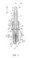
- FIG. 1 is a sectional view of an example of a spark plug manufactured by a manufacturing method of an embodiment.
- a line CL shown in FIG. 1 represents the center axis of the spark plug 100.
- the illustrated section contains the center axis CL.
- the center axis CL will also be referred to as the "axial line CL”
- the direction parallel to the center axis CL will also be referred to as the "axial direction.”
- the radial direction of a circle whose center is located at the center axis CL will simply be referred to the "radial direction”
- the circumferential direction of a circle whose center is located at the center axis CL will simply be referred to the "circumferential direction.”
- the forward direction D1 is a direction from a metallic terminal 40 toward electrodes 20 and 30 which will be described later.
- the forward direction D1 side of FIG. 1 will be referred to as the forward end side of the spark plug 100, and the rearward direction D2 side of FIG. 1 will be referred to as the rear end side of the spark plug 100.
- the spark plug 100 includes an insulator 10 (hereinafter also referred to as the "ceramic insulator 10"), a center electrode 20, a ground electrode 30, a metallic terminal 40, a metallic shell 50, an electrically conductive first seal portion 60, a resistor 70, a covering portion 290, an electrically conductive second seal portion 80, a forward-end-side packing 8, talc 9, a first rear-end-side packing 6, and a second rear-end-side packing 7.
- the insulator 10 is a generally cylindrical member having a through hole 12 (hereinafter also referred to as the "axial hole 12") extending along the center axis CL and penetrating the insulator 10.
- the insulator 10 is formed by firing alumina (other insulating materials can be employed).
- the insulator 10 has a leg portion 13, a first outer-diameter decreasing portion 15, a forward-end-side trunk portion 17, a flange portion 19, a second outer-diameter decreasing portion 11, and a rear-end-side trunk portion 18, which are arranged in this order from the forward end side toward the rearward direction D2 side.
- the outer diameter of the first outer-diameter decreasing portion 15 decreases gradually from the rear end side toward the forward end side.
- An inner-diameter decreasing portion 16 whose inner diameter decreases gradually from the rear end side toward the forward end side is formed in the vicinity of the first outer-diameter decreasing portion 15 of the insulator 10 (at the forward-end-side trunk portion 17 in the example of FIG. 1 ).
- the outer diameter of the second outer-diameter decreasing portion 11 decreases gradually from the forward end side toward the rear end side.
- the rod-shaped center electrode 20 extending along the center axis CL is inserted into a forward end portion of the axial hole 12 of the insulator 10.
- the center electrode 20 has a leg portion 25, a flange portion 24, and a head portion 23 which are arranged in this order from the forward end side toward the rearward direction D2 side.
- a forward end portion of the leg portion 25 projects from the axial hole 12 on the forward end side of the insulator 10.
- the remaining portion of the center electrode 20 is disposed in the axial hole 12.
- a surface of the flange portion 24 on the forward direction D1 side is supported by the inner-diameter decreasing portion 16 of the insulator 10.
- the center electrode 20 includes an electrode base member 21 and a core 22 embedded in the electrode base member 21.
- the electrode base member 21 is formed of, for example, Inconel (registered trademark) which is an alloy containing nickel as a main component.
- the core 22 is formed of a material (for example, an alloy containing copper) which is higher in thermal conductivity than the electrode base member 21.
- the metallic terminal 40 is inserted into a rear end portion of the axial hole 12 of the insulator 10.
- the metallic terminal 40 is formed of an electrically conductive material (for example, metal such as low-carbon steel).
- the metallic terminal 40 has a cap attachment portion 41, a flange portion 42, and a leg portion 43 which are arranged in this order from the rear end side toward the forward direction D1 side.
- the cap attachment portion 41 projects from the axial hole 12 on the rear end side of the insulator 10.
- the leg portion 43 is inserted into the axial hole 12 of the insulator 10.
- the circular columnar resistor 70 for suppressing electrical noise is disposed in the axial hole 12 of the insulator 10 to be located between the metallic terminal 40 and the center electrode 20.
- the electrically conductive first seal portion 60 is disposed between the resistor 70 and the center electrode 20, and the electrically conductive second seal portion 80 is disposed between the resistor 70 and the metallic terminal 40.
- the center electrode 20 and the metallic terminal 40 are electrically connected through the resistor 70 and the seal portions 60 and 80. Since the seal portions 60 and 80 are provided, the contact resistances among the stacked members 20, 60, 70, 80, and 40 become stable, and the electrical resistance between the center electrode 20 and the metallic terminal 40 becomes stable.
- the resistor 70 is formed through use of, for example, particles of glass (e.g., B 2 O 3 -SiO 2 glass) (main component), particles of ceramic (e.g., TiO 2 ), and an electrically conductive material (e.g., Mg).
- the seal portions 60 and 80 are formed through use of, for example, particles of glass similar to that used for the resistor 70 and particles of metal (e.g., Cu).
- the metallic shell 50 is a generally cylindrical member having a through hole 59 which extends along the center axis CL and penetrates the metallic shell 50.
- the metallic shell 50 is formed of low-carbon steel (other electrically conductive materials (e.g., metallic material) can be employed).
- the insulator 10 is inserted into the through hole 59 of the metallic shell 50.
- the metallic shell 50 is fixed to the outer periphery of the insulator 10.
- a forward end of the insulator 10 projects from the through hole 59.
- a rear end of the insulator 10 projects from the through hole 59.
- the metallic shell 50 has a trunk portion 55, a seat portion 54, a deformable portion 58, a tool engagement portion 51, and a crimp portion 53 arranged in this order from the forward end side toward the rear end side.
- the seat portion 54 is a flange-shaped portion.
- a screw portion 52 for screw engagement with an attachment hole of an internal combustion engine (e.g., gasoline engine) is formed on the outer circumferential surface of the trunk portion 55.
- An annular gasket 5 formed by bending a metal plate is fitted between the seat portion 54 and the screw portion 52.
- the metallic shell 50 has an inner-diameter decreasing portion 56 disposed on the forward direction D1 side of the deformable portion 58.
- the inner diameter of the inner-diameter decreasing portion 56 decreases gradually from the rear end side toward the forward end side.
- the forward-end-side packing 8 is sandwiched between the inner-diameter decreasing portion 56 of the metallic shell 50 and the first outer-diameter decreasing portion 15 of the insulator 10.
- the forward-end-side packing 8 is an 0-ring formed of iron (other materials (e.g., metallic material such as copper) can be employed).
- the tool engagement portion 51 has a shape (e.g., a hexagonal column) suitable for engagement with a spark plug wrench.
- the crimp portion 53 is provided on the rear end side of the tool engagement portion 51.
- the crimp portion 53 is disposed on the rear end side of the second outer-diameter decreasing portion 11 of the insulator 10, and forms a rear end (an end on the rearward direction D2 side) of the metallic shell 50.
- the crimp portion 53 is bent radially inward.
- an annular space SP is formed between the inner circumferential surface of the metallic shell 50 and the outer circumferential surface of the insulator 10.
- this space SP is a space surrounded by the crimp portion 53 and the tool engagement portion 51 of the metallic shell 50 and the second outer-diameter decreasing portion 11 and the rear-end-side trunk portion 18 of the insulator 10.
- the first rear-end-side packing 6 is disposed in the space SP to be located on the rear end side thereof.
- the second rear-end-side packing 7 is disposed in the space SP to be located on the forward end side thereof.
- these rear-end-side packings 6 and 7 are C-rings formed of irons (other materials can be employed). Powder of the talc 9 is changed between the two rear-end-side packings 6 and 7 within the space SP.
- the spark plug 100 When the spark plug 100 is manufactured, crimping is performed such that the crimp portion 53 is bent inward. Thus, the crimp portion 53 is pressed toward the forward direction D1 side. As a result, the deformable portion 58 deforms, and the insulator 10 is pressed forward within the metallic shell 50 via the packings 6 and 7 and the talc 9.
- the forward-end-side packing 8 is pressed between the first outer-diameter decreasing portion 15 and the inner-diameter decreasing portion 56 to thereby establish a seal between the metallic shell 50 and the insulator 10.
- the ground electrode 30 is joined to a forward end (an end on the forward direction D1 side) of the metallic shell 50.
- the ground electrode 30 is a rod-shaped electrode.
- the ground electrode 30 extends in the forward direction D1 from the metallic shell 50, bends toward the center axis CL, and has a distal end portion 31.
- the distal end portion 31 forms a gap g in cooperation with a forward end surface 20s1 of the center electrode 20 (the surface 20s1 is located on the forward direction D1 side).
- the ground electrode 30 is joined to the metallic shell 50 such that the ground electrode 30 electrically communicates with the metallic shell 50 (for example, laser welding).
- the ground electrode 30 has a base member 35 which forms the surface of the ground electrode 30, and a core 36 embedded in the base member 35.
- the base member 35 is formed of, for example, Inconel, and the core 36 is formed of a material (e.g., pure copper) which is higher in thermal conductivity than the base member 35.
- annular space Sf is formed between the metallic shell 50 (the trunk portion 55 in the present embodiment) and the insulator 10 (the leg portion 13 in the present embodiment).
- the center of the annular space Sf coincides with the center axis CL, and the annular space Sf opens toward the forward direction D1 side.
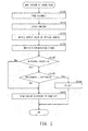
- FIG. 2 is a flowchart showing an example of a manufacturing method of the embodiment.
- an assembly is formed.
- the assembly is a semi-finished produce of the completed spark plug 100 shown in FIG. 1 in a state before the ground electrode 30 is bent.
- Various known methods can be employed so as to form the assembly. For example, a method described below can be employed.
- the insulator 10, the center electrode 20, the ground electrode 30, the metallic terminal 40, and the metallic shell 50 are manufactured.
- a straight, unbent member is manufactured as the ground electrode 30.
- Various known methods can be employed so as to manufacture these members 10, 20, 30, 40, and 50, and their detailed descriptions are omitted. Notably, at least some members may be prepared by purchasing them rather than manufacturing them.
- the center electrode 20 is disposed in the axial hole 12 at a position at which the center electrode 20 is supported by the inner-diameter decreasing portion 16 ( FIG. 1 ).
- material powder of the first seal portion 60, material powder of the resistor 70, and material powder of the second seal portion 80 are charged into the axial hole 12 in this order.
- the insulator 10 is heated to a predetermined temperature higher than the softening points of the glass components contained in the material powders.
- the metallic terminal 40 is inserted into the axial hole 12 from an opening of the axial hole 12 on the rearward direction D2 side.
- the material powders are compressed and fired, whereby the first seal portion 60, the resistor 70, and the second seal portion 80 are formed.
- the metallic shell 50 is fixed to the insulator 10.
- the method described with reference to FIG. 1 can be employed for the fixation.
- the straight, unbent ground electrode 30 is fixed to the forward end of the metallic shell 50.
- welding can be employed so as to fix the ground electrode 30.
- the metallic shell 50 may be fixed to the insulator 10 after fixing the ground electrode 30 to the metallic shell 50.
- the assembly is formed by the above-described procedure.
- FIG. 3 is a schematic view of a testing apparatus 900.
- the testing apparatus 900 has a test bench 200 to which an assembly 100x is attached, an optical sensor 300, a power supply apparatus 400 which applies a voltage to the assembly 100x, and a processing apparatus 500 which performs data processing.
- the power supply apparatus 400 has a voltage application circuit 410 which outputs a voltage for discharge, and a differentiating circuit 420 which obtains the time-differentiated value of the output voltage.
- the processing apparatus 500 has an AD converter 510 which converts an analog signal to digital data, and a data processing section 520 which executes data processing.
- the data processing section 520 is, for example, a computer including a CPU and a storage device.
- FIG. 3 a schematic sectional view of the test bench 200 is shown.
- the center axis CL and the directions D1 and D2 in FIG. 3 are shown to match the direction of the assembly 100x attached to the test bench 200.
- the cross section of the test bench 200 contains the center axis CL.
- the test bench 200 includes a container 210, a window member 220, and a window frame 230.
- the container 210 has an attachment hole 212 for attachment of the assembly 100x, an accommodation chamber 214 for accommodating a forward end portion of the assembly 100x attached to the attachment hole 212, and an opening 216 disposed at one end of the accommodation chamber 214 on the forward direction D1 side.
- the opening 216 is closed by the window member 220.
- the window member 220 is formed of a transparent material (glass in the present embodiment).
- the window frame 230 is disposed on the forward direction D1 side of the window member 220.
- the window frame 230 is a looped member for supporting the entire circumferential edge of the window member 220.
- the window member 220 is fixed to the container 210 while being sandwiched between the container 210 and the window frame 230. From the forward direction D1 side of the window member 220, the forward end portion of the assembly 100x can be observed through the window member 220.
- the optical sensor 300 is disposed on the forward direction D1 side of the window member 220.
- the optical sensor 300 is a sensor which outputs an output value corresponding to the intensity of light (i.e., brightness).
- the optical sensor 300 is a photo diode which outputs a current corresponding to the intensity of light.
- the optical sensor 300 is disposed on the forward direction D1 side of the window member 220 to be located on the center axis CL.
- the light receiving surface (not shown) of the optical sensor 300 on the center axis CL faces toward the rearward direction D2 side ; i.e., faces toward the forward end portion of the assembly 100x.
- High-voltage cables 431 and 432 are connected to the voltage application circuit 410 of the power supply apparatus 400. These high-voltage cables 431 and 432 are connected to the metallic terminal 40 and the metallic shell 50, respectively, of the assembly 100x.
- the voltage application circuit 410 applies a voltage between the metallic terminal 40 and the metallic shell 50 through the high-voltage cables 431 and 432. Since the metallic terminal 40 is electrically connected to the center electrode 20, the voltage is applied between the center electrode 20 and the metallic shell 50. When the voltage is applied between the center electrode 20 and the metallic shell 50, discharge may occur in the space Sf between the metallic shell 50 and the insulator 10 in some cases.
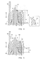
- FIGS. 4 and 5 are schematic sectional views showing paths of discharge which may occur in the forward end portion of the assembly 100x.
- Each of these drawings shows a cross section of the forward end portion of the assembly 100x (specifically, a cross section containing the center axis CL).
- Paths Pt1 and Pt2 indicated by thick lines show examples of the paths of discharge.
- FIG. 4 shows the first discharge path Pt1.
- the first discharge path Pt1 extends from an inner circumferential surface 50i of the metallic shell 50, reaches a surface 10o of the insulator 10, extends along the surface 10o of the insulator 10 toward the forward direction D1 side, passes over a forward end surface 101 of the insulator 10, and reaches the center electrode 20.
- This first discharge path Pt1 is an example of the path of creeping discharge.
- the space Sf between the inner circumferential surface 50i of the metallic shell 50 and the surface 10o of the insulator 10 is formed on the forward direction D1 side of a region where the forward-end-side packing 8 is provided as a seal.
- the distance between the inner circumferential surface 50i of the metallic shell 50 and the surface 10o of the insulator 10 is smaller than those in other regions within the space Sf.
- a discharge which passes through a discharge path which extends from a portion of the inner circumferential surface 50i of the metallic shell 50 located on the forward direction D1 side of the forward-end-side packing 8, extends along the surface 10o of the insulator 10, and reaches the center electrode 20; i.e., the first discharge path Pt1 of FIG. 4 .
- the metallic shell 50 has an inner-diameter increasing portion 57 which is located on the forward direction D1 side of the inner-diameter decreasing portion 56 and at which the inner diameter increases toward the forward direction D1 side.
- the inner diameter is approximately constant on the forward direction D1 side of the inner-diameter increasing portion 57.
- the inner diameter is approximately constant between the inner-diameter increasing portion 57 and the inner-diameter decreasing portion 56.
- the inner-diameter decreasing portion 56 and the inner-diameter increasing portion 57 form a projection which projects radially inward.
- an end of the inner-diameter increasing portion 57 on the rearward direction D2 side forms a projection 567.
- discharge which passes through the projection is likely to be generated.
- the first discharge path Pt1 of FIG. 4 passes through the projection 567.
- the ground electrode 30x of the assembly 100x is straight; i.e., in a state before being bent.
- the distance between the ground electrode 30x and the center electrode 20 is greater than the distance between the surface 10o of the insulator 10 and the center electrode 20. Discharge between the ground electrode 30x and the center electrode 20 is less likely to occur as compared with discharge between the metallic shell 50 and the center electrode 20. Also, creeping discharge as shown in FIG. 4 may occur even when the insulation performance of the insulator 10 is good.
- FIG. 5 shows the second discharge path Pt2.
- an unintended through hole 131 is formed in the leg portion 13 of the insulator 10 and extends between the surface 10o and the axial hole 12.
- This unintended through hole 131 is a hole formed by discharge.
- a voltage is applied between the center electrode 20 and the metallic shell 50, such a through hole 131 may be formed, and there may occur a discharge which passes through the through hole 131; i.e., a discharge which penetrates the insulator 10.
- This second discharge path Pt2 is an example of the path of penetration discharge.
- the fact that a penetration discharge occurs upon application of a voltage for test means that the insulation of the insulator 10 is easily broken; i.e., the insulation performance of the insulator 10 is low.
- the length of a portion of the discharge path Pt2 of penetration discharge ( FIG. 5 ), which portion is exposed to the outside of the insulator 10, is shorter than the length of a portion of the discharge path Pt1 of creeping discharge ( FIG. 4 ), which portion is exposed to the outside of the insulator 10. Accordingly, in the chase where a penetration discharge occurs, the discharge is observed to be darker as compared with the case where a creeping discharge occurs. As will be described later, in the procedure of FIG. 2 , the test for judging whether or not a penetration discharge has occurred; i.e., for testing the insulation performance of the insulator 10, is performed by making use of a difference in brightness at the time of discharge.
- step S110 of FIG. 2 first, the assembly 100x is attached to the test bench 200 ( FIG. 3 ).
- a carbon dioxide gas is supplied to the accommodation chamber 214 of the container 210 through an unillustrated gas flow passage, whereby the pressure within the accommodation chamber 214 is increased to 3 MPa.
- the voltage application circuit 410 of the power supply apparatus 400 applies a voltage between the metallic terminal 40 and the metallic shell 50 of the assembly 100x. In some cases, no discharge occurs even when the voltage is applied. Also, creeping discharge as shown in FIG. 4 may occur. Also, penetration discharge as shown in FIG. 5 may occur.
- the processing apparatus 500 obtains an output value from the optical sensor 300 at the time when the voltage is applied.
- the AD converter 510 converts an analog output signal (current value in the present embodiment) from the optical sensor 300 to digital data.
- the data processing section 520 obtains the digital data converted from the analog output signal.
- the digital data represents the output value output from the optical sensor 300; i.e., the intensity of light measured by the optical sensor 300. In the case where no discharge has occurred, digital data representing a low intensity (dark) is obtained. In the case where creeping discharge ( FIG. 4 ) has occurred, digital data representing a high intensity (bright) is obtained. When penetration discharge ( FIG. 5 ) has occurred, digital data representing an intensity between the two intensities is obtained.
- the data processing section 520 obtains an output value representing the highest intensity in a period between the start and end of voltage application (hereinafter referred to as the "voltage application period"), as an output value representing the brightness of discharge.
- the data processing section 520 of the processing apparatus 500 obtains a discrimination signal from the power supply apparatus 400.
- the differentiating circuit 420 of the power supply apparatus 400 obtains the absolute value of the differentiated value of the voltage output from the voltage application circuit 410 (hereinafter referred to as the "absolute differentiated value"). Subsequently, the differentiating circuit 420 supplies to the processing apparatus 500 a signal indicating whether or not the absolute differentiated value exceeds a predetermined derivative threshold in the voltage application period, as a discrimination signal. In the case where no discharge occurs, since the voltage changes gradually, the absolute differentiated value is equal to or less than the derivative threshold.
- the absolute differentiated value exceeds the derivative threshold.
- the fact that the absolute differentiated value exceeds the derivative threshold during the voltage application period means that a discharge has occurred, and the fact that the absolute differentiated value is equal to or less than the derivative threshold during the voltage application period means that no discharge has occurred.
- next step S130 the data processing section 520 of the processing apparatus 500 judges whether or not a discharged has occurred on the basis of the discrimination signal. In the case where no discharge has occurred (namely, the absolute differentiated value is equal to or less than the threshold), the insulation performance of the insulator 10 is presumed to be good. In this case, in the next step S150, the ground electrode 30 is bent toward the center electrode 20 and the gap g is formed. Thus, the park plug 100 is completed, and the processing of FIG. 2 ends.
- the data processing section 520 of the processing apparatus 500 judges whether or not the output value obtained in step S120 shows that the intensity of light is equal to or less than a predetermined brightness threshold.
- the output value (current value) of the optical sensor 300 has a positive correlation with the intensity of light. Accordingly, when the output value is equal to or less than a predetermined output threshold, the data processing section 520 judges that the output value shows that the intensity of light is equal to or less than the brightness threshold.
- the output threshold is a threshold value corresponding to the brightness threshold.
- the discharge is creeping discharge ( FIG. 4 ) and the insulation performance of the insulator 10 is presumed to be good.
- the ground electrode 30 is bent toward the center electrode 20 and the gap g is formed.
- the judgment as to whether or not a penetration discharge penetrating the insulator 10 has occurred is made through use of an output value which is output from the optical sensor 300 directed toward the forward end of the assembly 100x during a period during which a voltage is applied between the metallic shell 50 and the center electrode 20 of the assembly 100x. Accordingly, it is possible to prevent occurrence of a situation where an erroneous judgment that a penetration discharge has occurred is made despite that a creeping discharge has actually occurred. As a result, the accuracy of the judgment as to whether or not a penetration discharge has occurred can be increased.
- the gap g between the ground electrode 30 and the center electrode 20 is formed by bending the ground electrode 30x (S150). Accordingly, the spark plug 100 can be manufactured properly. Also, in the case where it is judged that a penetration discharge has occurred (S140: Yes), the assembly 100x is not employed for manufacture of the spark plug 100 (S160). Therefore, the possibility that a defective spark plug 100 is manufactured can be decreased. For example, it is possible to restrain manufacture of a spark plug 100 in which a penetration discharge is likely to occur.
- the conditions for judging occurrence of penetration discharge include a condition that the output value from the optical sensor 300 shows that the intensity of light (i.e., brightness) is equal to or less than the predetermined brightness threshold (S140). Accordingly, proper judgment can be realized.
- FIG. 6 is a graph showing the results of a first evaluation test performed by using samples of the assembly 100x.
- the horizontal axis shows the types of the samples of the assembly 100x, and the vertical axis shows the intensity of light.
- the intensity of light shows the output value from the optical sensor 300.
- the output value is shown as a ratio to a predetermined value. The output value was obtained by using the testing apparatus 900 of FIG. 3 under the following conditions.
- the presence/absence of an unintended through hole in the leg portion 13 of the insulator 10 was checked by a liquid penetrant flaw detection test.
- 100 samples in which no unintended through hole had been detected were obtained as 100 samples of an assembly in which no through hole was formed as a result of the test (hereinafter referred to the "assembly having no hole”).
- 100 samples in each of which an unintended through hole had been detected were obtained as 100 samples of an assembly in which a through hole was formed as a result of the test (hereinafter referred to the "assembly having a hole”).
- the graph of FIG. 6 shows the average, maximum value, and minimum value of the light intensity (output value) for the two types of samples obtained as described above.
- the light intensity of the assembly having no hole is greater than that of the assembly having a hole. This is because, as having been described with reference to FIGS. 4 and 5 , a creeping discharge occurred in the assembly having no hole, and a penetration discharge occurred in the assembly having a hole.
- the width of distribution of the light intensity of the assembly having no hole (the maximum value - the minimum value) is smaller than that of the assembly having a hole.
- this phenomenon has occurred for the following reason. Namely, in all the samples in which creeping discharges occurred, the discharge path of creeping discharge is approximately the same as the first discharge path Pt1 of FIG. 4 . Accordingly, the variation of the light intensity among the plurality of samples is relatively small. Meanwhile, in the samples in which penetration discharges occurred, the position of the through hole 131 (in particular, the position in the forward direction D1) differs among the samples. Accordingly, the length of a portion of the discharge path Pt2 ( FIG. 5 ) exposed to the outside of the insulator 10 also differs among the samples. As a result, the variation of the light intensity among the plurality of samples is relatively large.
- the minimum value VL of the light intensity of the assembly having no hole is greater than the maximum value VH of the light intensity of the assembly having a hole. Accordingly, the judgment as to whether or not a penetration discharge has occurred can be made accurately by employing, as the output threshold ( FIG. 2 : S140), a value which is greater than the maximum value VH and less than the minimum value VL. In the example of FIG. 6 , a value which is 0.5 times the average of the output values of the assembly having no hole can be employed as the output threshold.
- the distribution of the output value may change depending on the structure of the spark plug 100 and the spectral sensitivity characteristic of the optical sensor 300.
- the minimum value VL of the light intensity of the assembly having no hole is less than the maximum value VH of the light intensity of the assembly having a hole.
- various values can be employed as the brightness threshold (i.e., the output threshold).
- the lower the brightness threshold the lower the possibility that a creeping discharge is erroneously judged to be a penetration discharge.
- the brightness threshold is set to the minimum value VL of FIG. 6 , it is possible to reduce the possibility that the assembly having no hole is thrown away.
- the higher the brightness threshold the lower the possibility that a penetration discharge is erroneously judged to be a creeping discharge.
- the brightness threshold is set to the maximum value VH, it is possible to reduce the possibility that the spark plug 100 is manufactured using the assembly having a hole.
- FIG. 7 is a graph showing the results of a second evaluation test performed by using samples of the assembly 100x.
- the horizontal axis shows cover length LA (unit: mm) which will be described later, and the vertical axis shows penetration discharge detection ratio (unit: %).
- the second evaluation test the relation between the cover length LA and the detection ratio was determined by using four types of optical sensors which differed in measurement wavelength range (hereinafter also referred to as the "measurement wavelength band").
- the cover length LA is a length, as measured in parallel to the center axis CL, between the forward end 50f of the metallic shell 50 and the boundary 157 between the forward-end-side trunk portion 17 and the first outer-diameter decreasing portion 15 of the insulator 10.
- samples having cover lengths LA of 4, 5, 6, 8, 10, 12, 13, 14, 15, 16, and 17 were tested.
- These cover lengths LA were realized by changing the length of the trunk portion 55 of the metallic shell 50.
- a chamfered connection portion is present between the forward-end-side trunk portion 17 and the first outer-diameter decreasing portion 15.
- the boundary 157 is determined as follows.
- a straight portion 15L of the surface of the first outer-diameter decreasing portion 15 and a straight portion 17L of the surface of the forward-end-side trunk portion 17 are extended so that the two straight portions 15L and 17L intersect with each other at a certain point. This point of intersection is employed as the boundary 157.
- the configuration of the insulator 10 is common among the samples having the different cover lengths LA. In all the samples having the different cover lengths LA, the forward end surface 101 of the insulator 10 was located on the forward direction D1 side in relation to the forward end 50f of the metallic shell 50.
- the penetration discharge detection ratio was calculated as follows. As in the first evaluation test, of a plurality of samples which were judged by the discrimination signal to have generated discharge, 100 samples of the assembly having no hole were obtained through a flaw detection test. A value which was 0.5 times the average of the output values of the samples of the assembly having no hole was employed as the output threshold. Next, the output value of each of the samples which were judged by the discrimination signal to have generated discharge was compared with the output threshold in a manner similar to that in step S140 of FIG. 2 , to thereby judge, on the basis of the output value, whether or not a penetration discharge has occurred. Then, 100 samples which were judged on the basis of the output value to have suffered penetration discharge were obtained.
- a flaw detection test was performed on these 100 samples, and the number of assemblies (samples) having holes was counted. The ratio of the number of the assemblies (samples) having holes to the total number (100) of the samples was calculated as the penetration discharge detection ratio. The determination of the output threshold and the calculation of the detection ratio were performed for each of combinations of the wavelength ranges and the cover lengths LA.
- the four measurement wavelength ranges are as follows.
- the detection ratio tends to increase with the cover length LA. Presumably, this trend occurs for the following reason. Namely, as shown in FIG. 4 , creeping discharge creeps along the forward end surface 101 of the insulator 10. Accordingly, irrespective of the cover length LA, the discharge can be observed from the outside of the space Sf. As a result, when a creeping discharge occurs, a strong intensity is measured irrespective of the cover length LA. In contrast, as shown in FIG. 5 , a penetration discharge may occur in an inner part (i.e., a part on the rearward direction D2 side) of the space Sf. Accordingly, the greater the cover length LA, the greater the difficulty in observing the discharge from the outside of the apace Sf.
- the longer the cover length LA the lower the measured light intensity.
- the longer the cover length LA the greater the difference between the intensity of light produced as a result of creeping discharge and the intensity of light produced as a result of penetration discharge.
- the longer the cover length LA the higher the detection ratio.
- the detection ratio was satisfactory over a wider range of the cover length LA as compared with the case where other wavelength ranges (a range of 190 nm or grater and a range of 300 nm or greater) were used. Accordingly, in order to realize satisfactory detection ratios in a wide range of the cover length LA, it is preferred to use the wavelength range of 320 nm or greater as the measurement wavelength range.
- the upper limit of the measurement wavelength range is as follows.
- the upper limit of the second wavelength range which realized satisfactory detection ratios is 1000 nm. Accordingly, it is preferred that a range of 1000 nm or less be used as the measurement wavelength range.
- the first wavelength range and the third wavelength range are the same in the lower limit of the wavelength range and differ in the upper limit of the wavelength range. However, as shown in FIG. 7 , in the first wavelength range and the third wavelength range, substantially the same detection ratio is attained at each value of the cover length LA. Namely, even when the upper limit of the wavelength range changes between 1000 nm and 680 nm, presumably, a change in the detection ratio is small.
- the measurement wavelength range may be 320 nm to 1000 nm.
- the measurement wavelength range may be 320 nm to 680 nm.
- the cover lengths LA at which satisfactory detection ratios (70% or greater) are obtained through use of the second wavelength range were 5, 6, 8, 10, 12, 13, 14, 15, 16, and 17 (unit: mm).
- An arbitrary value of these values may be employed as the lower limit of a preferred range of the cover length LA.
- an arbitrary value which is selected from these values and is greater than the lower limit may be employed as the upper limit of the preferred range of the cover length LA.
- the detection ratio was less than 70% when the cover length LA was 13 mm or less.
- a satisfactory detection ratio can be realized by setting the measurement wavelength range to the above-mentioned preferred range.
- a range of 5 mm to 13 mm may be employed as a preferred range of the cover length LA.
- the above-mentioned preferred range of the measurement wavelength range and the above-mentioned preferred range of the cover length LA can be applied to the manufacturing method of FIG. 2 .
- FIG. 8 is a graph showing the results of a third evaluation test performed by using a sample of the assembly 100x.
- the horizontal axis shows symbols FA to FK representing layout configurations of an optical sensor(s) 300, and the vertical axis shows the penetration discharge detection ratio (unit: %).
- the third evaluation test the relation between the layout of one or more optical sensors 300 and the detection ratio was determined.
- the cover length LA of the sample was 11 mm.
- the measurement wavelength range of the optical sensors was 320 nm to 1000 nm.
- the length, as measured in parallel to the center axis CL, of a portion of the insulator 10 projecting from the forward end 50f of the metallic shell 50 toward the forward direction D1 side was 3 mm.
- FIG. 9 is a table showing, for each of the 11 layout configurations FA to FK, the number of optical sensor(s) 300, the position(s) of the optical sensor(s) 300, and judgment conditions using the output value(s) of the optical sensors 300.
- the six positions P1 to P6 shown in the table are relative positions of the optical sensor(s) 300 in relation to the assembly 100x.
- FIGS. 10 and 11 are views used for explaining the relative positions P1 to P6.
- FIG. 10 is a schematic view of a forward end portion of the assembly 100x as viewed toward the center axis CL from a position away from the center axis CL.
- the ground electrode 30x is not shown.
- FIG. 11 is a schematic view of the forward end portion of the assembly 100x as viewed in the rearward direction D2. In FIG. 11 , the forward end 50f of the metallic shell 50 and the ground electrode 30x are shown, and other components are omitted.
- the first position P1 is the position of the optical sensor 300 described with reference to FIG. 3 , and is a position on the center axis CL which is located on the forward direction D1 side of the assembly 100x.
- the first position P1 will also be referred to as the "front position P1," and the optical sensor 300 at the first position P1 will also be referred to as the "front sensor 301.”
- the light receiving surface (not shown) of the front sensor 301 on the center axis CL faces the forward end portion of the assembly 100x (specifically, toward the rearward direction D2 side).
- the second position P2 through the sixth positions P6 are positions separated from the center axis CL; specifically, positions separated from the forward end portion of the assembly 100x in directions perpendicular to the center axis CL.
- the positions P2 to P6 separated from the center axis CL will also be referred to the "side positions P2 to P6," and the optical sensor(s) 300 at the side position(s) will also be referred to as the "side sensor(s) 302.”
- the light receiving surface (not shown) of each side sensor 302 does not intersect with the center axis CL, and faces the forward end portion of the assembly 100x from a position separated from the center axis CL.
- the side positions P2 to P6 are positions separated radially outward from the projecting portion of the insulator 10.
- the light receiving surface of each side sensor 302 faces in a direction toward the center axis CL, which direction is perpendicular to the center axis CL.
- the fifth position P5 is a position in a direction in which the ground electrode 30x is disposed as viewed from the center axis CL. As viewed from the center axis CL, the fifth position P5 is located behind the ground electrode 30x. When the assembly 100x is observed from the fifth position P5, a portion of the insulator 10 hides behind the ground electrode 30x.
- the third position P3 is a position located opposite the fifth position P5 with respect to the center axis CL.
- the second position P2 is a position in a direction orthogonal to the direction toward the fifth position P5 as viewed from the center axis CL.
- the fourth position P4 is a position located opposite the second position P2 with respect to the center axis CL.
- the sixth position P6 is a position between the second position P2 and the fifth position P5 as viewed from the center axis CL.
- the angle Ag26 between the direction from the center axis CL toward the second position P2 and the direction from the center axis CL toward the sixth position P6 is 30 degrees. Also, the angle Ag36 between the direction from the center axis CL toward the third position P3 and the direction from the center axis CL toward the sixth position P6 is 120 degrees. In the following description, the angle between the directions from the center axis CL toward the two side positions will be referred to as the "inter-sensor angle.”
- the layout of the optical sensor(s) 300 according to each of the layout configurations FA to FK is represented by using these relative positions P1 to P6.
- the first layout configuration FA is formed by using the first position P1
- the fifth layout configuration FE is formed by using two positions P2 and P4
- the eleventh layout configuration FK is formed by using three positions P1, P2, and P4.
- the judgment conditions are conditions for judging that a penetration discharge has occurred.
- the first condition J1 is applied to the layout configurations FA to FD whose number of sensors is "1.”
- the second condition J2 is applied to the layout configurations FE to FJ whose number of sensors is “2.”
- the third condition J3 is applied to the layout configurations FK whose number of sensors is "3.”
- the conditions J1, J2, and J3 are as follows.
- an output value which is 50% of the output value at the time of occurrence of creeping discharge is used as the output threshold.
- the output value of the optical sensor 300 is equal to or less than the output threshold; i.e., the light intensity detected by the optical sensor 300 is equal to or less than the brightness threshold, it is judged that a penetration discharge has occurred.
- two or three single optical sensors 300 when the output values of all the optical sensors 300 are equal to or less than the output threshold; i.e., all the light intensities detected by the optical sensors 300 are equal to or less than the brightness threshold, it is judged that a penetration discharge has occurred.
- the output value of at least one optical sensor 300 is greater than the output threshold, it is judged that a creeping discharge has occurred.
- any of these conditions J1, J2, and J3 can be employed as the judgment condition of step S140 of FIG. 2 .
- the output threshold was determined as follows. First, there was prepared a test bench (not shown) which allows observation of the forward end portion of the assembly 100x from the side positions P2 to P6 in addition to the front position P1. The optical sensor 300 was fixedly disposed at each of the positions P1 to P6. Subsequently, the assembly 100x was attached to the test bench, and the pressure within the accommodation chamber accommodating the forward end portion of the assembly 100x was increased through use of a carbon dioxide gas. Also, the high voltage cables 431 and 432 from the power supply apparatus 400 ( FIG. 3 ) are connected to the metallic terminal 40 and the metallic shell 50 of the assembly 100x. The voltage applied by the power supply apparatus 400 and the pressure within the accommodation chamber were adjusted such that a creeping discharge occurs at all times.
- the penetration discharge detection ratio was calculated as follows.
- the assembly 100x was attached to the test bench, and the voltage and the pressure within the accommodation chamber (i.e., the pressure of the carbon dioxide gas) were adjusted in accordance with the condition under which creeping discharge occurred at all times. Subsequently, the pressure was increased. Thus, creeping discharge was restrained. In this state, a voltage was applied between the center electrode 20 and the metallic shell 50 of the assembly 100x. Subsequently, as in the case of the first evaluation test, the output value of each optical sensor 300 was obtained. In the case where the discrimination signal showed generation of a discharge, in accordance with the above-described conditions J1 to J3, the judgment as to whether a penetration discharge had occurred was made on the basis of the output value.
- the detection ratio of the first layout configuration FA formed by using the front position P1 is better than the detection ratios of the layout configurations FB to FD formed by using the side sensors.
- the reason for this result is as follows. In the case where a creeping discharge occurs behind the insulator 10 as viewed from the side sensor(s) 302, it is difficult for the side sensor(s) 302 to receive light generated as a result of the discharge. Further, at the fifth position P5, it is difficult to receive a sufficient amount of light when a creeping discharge occurs in a region which is located behind the ground electrode 30x as viewed from the corresponding side sensor 302.
- the output value of the side sensor 302 may show a low intensity in some cases.
- the detection ratio becomes relatively low.
- the front sensor can receive light from the entire circumference of the surface 10o of the insulator 10 surrounding the center axis CL. Accordingly, when a creeping discharge occurs, an output value showing a strong intensity can be obtained from the front sensor. As a result, the detection ratio becomes relatively high.
- the detection ratios of the three layout configurations FE, FI, and FJ were better than the detection ratios of the remaining layout configurations FF, FG, and FH. The reason of this will be described below.
- the reason of the low (or bad) detection ratio of the sixth layout configuration FF including the fifth position P5 is presumably that the field of view of the side sensor 302 at the fifth position P5 is blocked by the ground electrode 30x. Also, the reason of the high (or good) detection ratio of the tenth layout configuration FJ including the front sensor 301 is presumably that the front sensor 301 can receive light from the entire circumference of the surface 10o of the insulator 10 surrounding the center axis CL.
- the layout configurations FE to FI having two side sensors 302 are as follows.
- the respective inter-sensor angles of these layout configurations FE to FI are as follows (excluding the sixth layout configuration FF).
- the detection ratio of the eleventh layout configuration FK whose number of sensors is "3" is the best among the detection ratios of the tested layout configurations FA to FK.
- the reason for this is that the eleventh layout configuration FK includes the front position P1 from which the entire circumference of the surface 10o of the insulator 10 surrounding the center axis CL can be observed and the two side positions P2 and P4 the angle (inter-sensor angle) between which is 180 degrees.
- Each of these Configurations 1 to 3 determines the relative positional relations) of the optical sensor(s) 300 in relation to the assembly 100x in consideration of the field(s) of view of the optical sensor(s) 300. Accordingly, it is presumed that when at least one of these Configurations 1 to 3 is employed, the detection ratio can be improved irrespective of the structure of the spark plug 100 and the structure of the testing apparatus 900 (for example, the cover length LA and the measurement wavelength range of each optical sensor 300).
- a layout configuration arbitrarily chosen from the layout configurations FA to FK shown in FIG. 9 can be applied to the manufacturing method of FIG. 2 .
- a condition corresponding to the layout configuration can be applied to the step S140 of FIG. 2 .
- FIG. 12 is a graph showing the results of a fourth evaluation test performed by using samples of the assembly 100x.
- the horizontal axis shows the position LC (unit: mm) of an unintended through hole 131 ( FIG. 5 ) which will be described later, and the vertical axis shows creeping discharge detection ratio (unit: %).
- the fourth evaluation test the relation between the position LC of the unintended through hole 131 and the detection ratio was determined.
- the structures of the testing apparatus for example, the test bench), the optical sensor(s) 300, and the assembly 100x which were used in the test are the same as those employed in the third evaluation test.
- the position LC of the unintended through hole 131 is the length (measured in parallel to the center axis CL) between the position of the through hole 131 on the surface 10o of the insulator 10 and the boundary 157 between the forward-end-side trunk portion 17 and the first outer-diameter decreasing portion 15 of the insulator 10.
- the position LC of the through hole 131 will also be referred to as the "hole position LC.”
- the hole position LC of the through hole 131 formed as a result of penetration discharge changes in accordance with the pressure within the accommodation chamber which accommodates the forward end portion of the assembly 100x. Specifically, the higher the pressure, the lower the possibility of generation of discharge; namely, the shorter the distance of the discharge path.
- the cover length LA of the assembly 100x ( FIG. 4 ) used in the fourth evaluation test was 11 mm, and the leg length LB thereof was 14 mm.
- the leg length LB is a length (measured in parallel to the center axis CL) between the boundary 157 and the forward end of the insulator 10. Therefore, the hole position LC of 13 mm is a position corresponding to the forward end 50f of the metallic shell 50. In the case where the hole position LC is greater than 13 mm, the through hole 131 is located on the forward direction D1 side of the forward end 50f of the metallic shell 50. In the case where the hole position LC is less than 13 mm, the through hole 131 is located on the rearward direction D2 side of the forward end 50f of the metallic shell 50.
- the fourth evaluation test the first layout configuration FA and the fifth layout configuration FE described with reference to FIG. 9 were tested as the layout of the optical sensors 300.
- the method of determining the output threshold is the same as that employed in the third evaluation test.
- the method of calculating the creeping discharge detection ratio is as follows. As in the case of the third evaluation test, the assembly 100x was attached to the test bench, and a voltage was applied. The output value of each optical sensor 300 was obtained. When the discrimination signal showed generation of a discharge, in accordance with the above-described conditions J1 to J3, the judgment as to whether or not a penetration discharge has occurred was made on the basis of the output value.
- Discharge was repeatedly generated until it was judged on the basis of the output value that a penetration discharge has occurred. Such repetition of discharge was performed for 100 samples. A flaw detection test was performed on the 100 samples, and the number of unintended holes was counted for each sample. If the result of the judgment on each of the discharges repeatedly generated is correct, the number of holes is one. However, in the case where it was erroneously judged on the basis of the output value that a penetration discharge has not occurred despite the fact that a penetration discharge has occurred, the number of holes increases with the number of times of erroneous judgment. Namely, the number of holes which is equal to or greater than 2 means that erroneous judgment was made one or more times.
- the ratio of samples in which the number of holes was 1 (namely, samples for which erroneously judgment was not made presumably) to the total number (100) of the samples was calculated as the detection ratio.
- calculation of the detection ratio was performed for each of the seven hole positions LC; i.e., for each of the seven pressures.
- the horizontal axis of the graph of FIG. 12 shows the hole position LC presumed from the pressure.
- a value obtained by rounding off the first decimal place of the measurement value of the hole position LC of a hole actually formed at each pressure was the same as the hole position LC presumed from the pressure.
- the detection ratio was better as compared with the case where the hole position LC was located on the forward direction D1 side.
- the reason for this is as follows.
- the intensity of light produced as a result of occurrence of penetration discharge is apt to become low as compared with the case where the hole position LC is located on the forward direction D1 side. Accordingly, the difference in light intensity between penetration discharge and creeping discharge is apt to become large.
- a good detection ratio is realized in the case where the hole position LC is located on the rearward direction D2 side.
- the fifth layout configuration FE was able to realize a better detection ratio as compared with the first layout configuration FA.
- the reason for this is as follows. Namely, since penetration discharge hides behind the metallic shell 50 when viewed from the side sensors 302, it is difficult for the side sensors 302 to receive light produced as a result of occurrence of penetration discharge. In contrast, since creeping discharge passes through the forward direction D1 side of the forward end 50f of the metallic shell 50, the side sensors 302 can receive light produced as a result of occurrence of creeping discharge. Accordingly, the difference in light intensity between penetration discharge and creeping discharge is relatively large.
- the fifth layout configuration FE using two side sensors 302 can realize a good detection ratio.
- the inter-sensor angle of the fifth layout configuration FE is 180 degrees, a dead spot of the surface 10o of the insulator 10 is small. Accordingly, a good detection ratio can be realized easily.
- the front sensor 301 can receive both the light produced as a result of occurrence of penetration discharge and the light produced as a result of occurrence of creeping discharge. Accordingly, the difference in light intensity between penetration discharge and creeping discharge is relatively small.
- the detection ratio of the first layout configuration FA which uses the front sensor 301 without using the side sensors 302 can become lower than the detection ratio of the fifth layout configuration FE.
- Various positions within a range within which the light receiving surface of the front sensor 301 intersects with the center axis CL can be employed as the position of the front sensor 301.
- FIG. 13 is a schematic view of the forward end portion of the assembly 100x as viewed from a position on the center axis CL.
- the ceramic insulator 10, the center electrode 20, and the metallic shell 50 are shown, and the ground electrode 30x is not shown.
- the ceramic insulator 10, the center electrode 20, and the metallic shell 50 are observed to form concentric circles whose centers coincide with the center axis CL.
- contours 109 and 509 are shown by thick lines.
- the contour 109 is the outer contour of a region in which the insulator 10 is observed (hereinafter referred to as the "insulator contour 109").
- the contour 509 is the inner contour of the forward end 50f of the metallic shell 50 (hereinafter referred to as the "shell contour 509").
- the positions of the contours 109 and 509 on the cross section are shown.
- the insulator contour 109 corresponds to a position in the vicinity of the end of the space Sf on the rearward direction D2 side (here, a position in the vicinity of the end of the inner-diameter increasing portion 57 of the metallic shell 50, the end being located on the rearward direction D2 side).
- the shell contour 509 corresponds to the edge of the forward end 50f on the inner side in the radial direction.
- the insulator contour 109 and the shell contour 509 can be viewed in a mutually separated state over the entire circumference surrounding the center axis CL.
- the space Sf is formed between the insulator contour 109 and the shell contour 509. Namely, from a position on the center axis CL, the space Sf can be observed over the entire circumference surrounding the center axis CL. Also, from a position on the center axis CL, substantially the entirety of an exposed portion of the surface 10o of the insulator 10; i.e., substantially the entirety of a portion of the surface 10o of the insulator 10 on the forward direction D1 side of the forward-end-side packing 8, can be observed.
- the optical sensor 300 Accordingly, from a position on the center axis CL, it is possible to observe discharge generated at an arbitrary position on the surface 10o of a portion of the insulator 10, the portion being located on the forward direction D1 side of the forward-end-side packing 8. Accordingly, the accuracy of the judgment as to whether or not a penetration discharge has occurred can be improved by disposing the optical sensor 300 at a position from which the insulator contour 109 and the shell contour 509 can be viewed in a mutually separated state over the entire circumference surrounding the center axis CL.
- FIG. 14 is a schematic view of the forward end portion of the assembly 100x as viewed from a position slightly deviated from the center axis CL.
- the insulator 10, the center electrode 20, and the metallic shell 50 are observed to be inclined.
- the contour 109x indicated by a thick line is the outer contour of the region where the insulator 10 is observed (hereinafter referred to as the "insulator contour 109x").
- a portion of the shell contour 509 hides behind the insulator 10.
- the insulator contour 109x is in contact with the shell contour 509.
- a portion of the space Sf hides behind the insulator 10 and cannot be observed.
- a portion of the surface 10o of the insulator 10 cannot be observed. Accordingly, in the case where a discharge occurs on a hidden portion of the surface 10o of the insulator 10, there is a possibility that a correct judgment cannot be performed.
- the forward end portion of the assembly 100x is observed from the front sensor 301, it is preferred that a position from which the insulator contour and the shell contour 509 can be viewed in a mutually separated state over the entire circumference surrounding the center axis CL be employed as the position of the front sensor 301.
- a position from which the insulator contour and the shell contour 509 can be viewed in a mutually separated state over the entire circumference surrounding the center axis CL be employed as the position of the front sensor 301.
- a position at which the insulator contour and the shell contour 509 can be viewed in a mutually separated state it is preferred to employ a position at which the insulator contour and the shell contour 509 can be viewed in a mutually separated state.
- the center of the light receiving surface there can be employed the position of the center of gravity determined under the assumption that the mass is uniformly distributed within the light receiving surface.
- the distal end portion 31 of the ground electrode 30 faces the forward end surface 20s1 of the center electrode 20, which surface faces toward the forward direction D1 side, to thereby form the gap g.
- the distal end portion of the ground electrode 30 may face the outer circumferential surface of the center electrode 20 to thereby form a gap.
- another conductor may be disposed between the ground electrode 30 and the metallic shell 50. In this case as well, the ground electrode 30 is electrically connected to the metallic shell 50 through the conductor.
- second seal portion 100 ... spark plug, 100x ... assembly, 101 ... forward end surface, 109, 109x ... insulator contour, 131 ... through hole, 157 ... boundary, 200 ... test bench, 210 ... container, 212 ... attachment hole, 214 ... accommodation chamber, 216 ... opening, 220 ... window member, 230 ... window frame, 300 ... optical sensor, 301 ... front sensor, 302 ... side sensor, 400 ... power supply apparatus, 410 ... voltage application circuit, 420 ... differentiating circuit, 431, 432 ... high voltage cable, 500 ... processing apparatus, 509 ... shell contour, 520 ... data processing section, 567 ... projection, 900 ... testing apparatus, g ... gap, CL axial line (center axis)
Abstract
Description
- The present invention relates to a method of manufacturing a spark plug.
- Conventionally, spark plugs have been used for internal combustion engines. Such a spark plug includes a center electrode extending in an axial direction thereof; an insulator having an axial hole extending in the axial direction and holding a center electrode inserted into a forward end portion of the axial hole; a metallic shell disposed around the insulator; and a ground electrode electrically communicating with the metallic shell. When such a spark plug is manufactured, the spark plug may be inspected to judge whether or not the spark plug is defective. For example, there has been proposed a method of testing the insulation performance (i.e., withstand voltage) of the insulator by producing a potential difference between the metallic shell and the center electrode in a state in which the spark plug is exposed to an atmosphere whose pressure is higher than the atmospheric pressure so as to suppress discharge. A judgment as to whether or not a discharge which penetrates the insulator (hereinafter referred to "penetration discharge") has occurred is made by utilizing a change in current at the time when a potential difference is produced between the metallic shell and the center electrode.
-
Patent Document 1 Japanese Patent Application Laid-Open (kokai) No.2012-185963 - However, when a potential difference is produced between the metallic shell and the center electrode, in some cases, generated discharge creeps along the surface of the insulator without penetrating the insulator (hereinafter, the discharge creeping along the surface of the insulator will be referred to as "creeping discharge"). When such a creeping discharge occurs, the waveform of current or voltage changes as in the case where a penetration discharge occurs. Accordingly, even in the case where penetration discharge does not occur; i.e., when the insulation performance of the insulator is sufficiently high, an erroneous judgment that a discharge penetrating the insulator has occurred is made because of occurrence of creeping discharge.
- A main object of the present invention is to improve the accuracy of a judgment as to whether or not a discharge penetrating an insulator has occurred.
- The present invention has been accomplished so as to solve, at least partially, the above-described problem, and the present invention can be embodied in the following application examples.
- A method of manufacturing a spark plug which includes a center electrode extending in an axial direction; an insulator having an axial hole which extends in the axial direction and in which the center electrode is disposed; a metallic shell disposed around the insulator; and a ground electrode electrically connected to the metallic shell and forming a gap between the ground electrode and the center electrode, the method being characterized by comprising:
- an assembly step of forming an assembly by combining the metallic shell, the insulator, and the center electrode;
- an application step of applying a voltage between the metallic shell and the center electrode of the assembly; and
- a judgment step of judging, in a period during which the voltage is applied, whether or not a discharge penetrating the insulator has occurred, by using an output value output from an optical sensor directed toward a forward end portion of the assembly.
- According to this configuration, the judgment as to whether or not a discharge penetrating the insulator has occurred is made by using the output value from the optical sensor. Accordingly, in the case where a discharge creeping along the surface of the insulator without penetrating the insulator has occurred, it possible to prevent this state from being erroneously judged that a discharge penetrating the insulator has occurred. As a result, the accuracy of the judgment as to whether or not a discharge penetrating the insulator has occurred can be improved.
- The manufacturing method described in the application example 1 is characterized in that
- the insulator has an outer-diameter decreasing portion where the outer diameter of the insulator decreases toward the forward end side in the axial direction, and a large diameter portion provided on the rear end side of the outer-diameter decreasing portion;
- the metallic shell has an inner-diameter decreasing portion where the inner diameter of the metallic shell decreases toward the forward end side in the axial direction;
- the assembly has a packing sandwiched between the outer-diameter decreasing portion and the inner-diameter decreasing portion;
- a length of the insulator, measured in parallel to the axial direction, between a forward end of the metallic shell and a boundary between the large diameter portion and the outer-diameter decreasing portion falls within a range of 5 mm to 13 mm; and
- in the judgment step, the output value output by using a wavelength band of 320 nm or greater is used.
- According to this configuration, even when the length of a part of the portion of the insulator on the forward end side of the boundary, which part is covered by the metallic shell, is short (13 mm or less), the accuracy of the judgment as to whether or not a discharge penetrating the insulator has occurred can be improved.
- The manufacturing method described in the application example 1 or 2 is characterized in that, in the judgment step, a plurality of optical sensors are used, the plurality of optical sensors including a front sensor which is an optical sensor located on the center axis of the assembly and directed toward the forward end portion of the assembly, and a side sensor which is an optical sensor located at a position separated from the center axis of the assembly and directed toward the forward end portion of the assembly.
- According to this configuration, the accuracy of the judgment as to whether or not a discharge penetrating the insulator has occurred can be improved by using the output value from the front sensor and the output value from the side sensor.
- The manufacturing method described in any of the application examples 1 to 3 is characterized in that
- in the judgment step, a plurality of optical sensors are used, the plurality of optical sensors including first and second side sensors which are optical sensors located at positions separated from the center axis of the assembly and directed toward the forward end portion of the assembly; and
- an angle between a direction from the center axis toward the first side sensor and a direction from the center axis toward the second side sensor is equal to or greater than 120 degrees.
- According to this configuration, the accuracy of the judgment as to whether or not a discharge penetrating the insulator has occurred can be improved by using the output value from the first side sensor and the output value from the second side sensor.
- The manufacturing method described in any of the application examples 1 to 4 is characterized in that
- in the judgment step, a front sensor located on the center axis of the assembly and directed toward the forward end portion of the assembly is used as the optical sensor;
- in the forward end portion of the assembly, an annular space is formed between the metallic shell and the insulator, the space having a center coinciding with the center axis and being open toward the forward end side; and
- the front sensor is disposed at a position at which an inner contour of the forward end of the metallic shell and an outer contour of the insulator can be viewed separately from each other.
- According to this configuration, the front sensor can properly output an output value which reflects the brightness of discharge irrespective of the position of the discharge. Therefore, the accuracy of the judgment as to whether or not a discharge penetrating the insulator has occurred can be improved
- The manufacturing method described in any of the application examples 1 to 5 is characterized in that
- in the judgment step, a side sensor located at a position separated from the center axis of the assembly and directed toward the forward end portion of the assembly is used as the optical sensor; and
- as viewed from the center axis of the assembly, the side sensor is disposed in a direction different from a direction in which the
ground electrode 30 is disposed. - According to this configuration, it is possible to restrain occurrence of a situation where discharge hides behind the ground electrode as viewed from the side sensor. Therefore, the accuracy of the judgment as to whether or not a discharge penetrating the insulator has occurred can be improved
- The manufacturing method described in any of the application examples 1 to 6 is characterized by further comprising a step of bending the ground electrode to thereby form the gap between the ground electrode and the center electrode in the case where it is judged in the judgment step that a discharge penetrating the insulator has not occurred.
- According to this configuration, in the case where it is judged in the judgment step that a discharge penetrating the insulator has not occurred, the gap is formed by bending the ground electrode. Therefore, the glow plug can be manufactured properly.
- The manufacturing method described in any of the application examples 1 to 7 is characterized in that conditions for judging, in the judgment step, that a discharge penetrating the insulator has occurred include a condition that the output value indicates that brightness is equal to or less than a predetermined threshold.
- According to this configuration, proper judgment can be realized.
- Notably, the present invention can be realized in various forms. For example, the present invention can be realized, for example, as a method of testing an assembly for a spark plug, a method of manufacturing a spark plug, or a spark plug manufactured by this manufacturing method.
-
-
FIG. 1 Sectional view of an example of a spark plug. -
FIG. 2 Flowchart showing an example of a method of manufacturing thespark plug 100. -
FIG. 3 Schematic view of atesting apparatus 900. -
FIG. 4 Schematic view showing a first discharge path Pt1. -
FIG. 5 Schematic view showing a second discharge path Pt2. -
FIG. 6 Graph showing the results of a first evaluation test. -
FIG. 7 Graph showing the results of a second evaluation test. -
FIG. 8 Graph showing the results of a third evaluation test. -
FIG. 9 Table showing layout configurations FA to FK, positions ofoptical sen sors 300, and judgment conditions. -
FIG. 10 Schematic view of a forward end portion of anassembly 100x. -
FIG. 11 Explanatory view showing relative positions P1 to P6. -
FIG. 12 Graph showing the results of a fourth evaluation test. -
FIG. 13 Schematic view of the forward end portion of theassembly 100x as viewed from a position on the center axis CL. -
FIG. 14 Schematic view of the forward end portion of theassembly 100x as viewed from a position slightly deviated from the center axis CL. -
FIG. 1 is a sectional view of an example of a spark plug manufactured by a manufacturing method of an embodiment. A line CL shown inFIG. 1 represents the center axis of thespark plug 100. The illustrated section contains the center axis CL. In the following description, the center axis CL will also be referred to as the "axial line CL," and the direction parallel to the center axis CL will also be referred to as the "axial direction." The radial direction of a circle whose center is located at the center axis CL will simply be referred to the "radial direction," and the circumferential direction of a circle whose center is located at the center axis CL will simply be referred to the "circumferential direction." Of directions parallel to the center axis CL, the downward direction inFIG. 1 will be referred to as a forward direction D1, and the upward direction will be referred to as a rearward direction D2. The forward direction D1 is a direction from ametallic terminal 40 towardelectrodes FIG. 1 will be referred to as the forward end side of thespark plug 100, and the rearward direction D2 side ofFIG. 1 will be referred to as the rear end side of thespark plug 100. - The
spark plug 100 includes an insulator 10 (hereinafter also referred to as the "ceramic insulator 10"), acenter electrode 20, aground electrode 30, ametallic terminal 40, ametallic shell 50, an electrically conductivefirst seal portion 60, aresistor 70, a covering portion 290, an electrically conductivesecond seal portion 80, a forward-end-side packing 8,talc 9, a first rear-end-side packing 6, and a second rear-end-side packing 7. - The
insulator 10 is a generally cylindrical member having a through hole 12 (hereinafter also referred to as the "axial hole 12") extending along the center axis CL and penetrating theinsulator 10. Theinsulator 10 is formed by firing alumina (other insulating materials can be employed). Theinsulator 10 has aleg portion 13, a first outer-diameter decreasing portion 15, a forward-end-side trunk portion 17, aflange portion 19, a second outer-diameter decreasing portion 11, and a rear-end-side trunk portion 18, which are arranged in this order from the forward end side toward the rearward direction D2 side. The outer diameter of the first outer-diameter decreasing portion 15 decreases gradually from the rear end side toward the forward end side. An inner-diameter decreasing portion 16 whose inner diameter decreases gradually from the rear end side toward the forward end side is formed in the vicinity of the first outer-diameter decreasing portion 15 of the insulator 10 (at the forward-end-side trunk portion 17 in the example ofFIG. 1 ). The outer diameter of the second outer-diameter decreasing portion 11 decreases gradually from the forward end side toward the rear end side. - The rod-shaped
center electrode 20 extending along the center axis CL is inserted into a forward end portion of theaxial hole 12 of theinsulator 10. Thecenter electrode 20 has aleg portion 25, aflange portion 24, and ahead portion 23 which are arranged in this order from the forward end side toward the rearward direction D2 side. A forward end portion of theleg portion 25 projects from theaxial hole 12 on the forward end side of theinsulator 10. The remaining portion of thecenter electrode 20 is disposed in theaxial hole 12. A surface of theflange portion 24 on the forward direction D1 side is supported by the inner-diameter decreasing portion 16 of theinsulator 10. Thecenter electrode 20 includes anelectrode base member 21 and a core 22 embedded in theelectrode base member 21. Theelectrode base member 21 is formed of, for example, Inconel (registered trademark) which is an alloy containing nickel as a main component. The core 22 is formed of a material (for example, an alloy containing copper) which is higher in thermal conductivity than theelectrode base member 21. - The
metallic terminal 40 is inserted into a rear end portion of theaxial hole 12 of theinsulator 10. Themetallic terminal 40 is formed of an electrically conductive material (for example, metal such as low-carbon steel). Themetallic terminal 40 has acap attachment portion 41, aflange portion 42, and aleg portion 43 which are arranged in this order from the rear end side toward the forward direction D1 side. Thecap attachment portion 41 projects from theaxial hole 12 on the rear end side of theinsulator 10. Theleg portion 43 is inserted into theaxial hole 12 of theinsulator 10. - The circular
columnar resistor 70 for suppressing electrical noise is disposed in theaxial hole 12 of theinsulator 10 to be located between themetallic terminal 40 and thecenter electrode 20. The electrically conductivefirst seal portion 60 is disposed between theresistor 70 and thecenter electrode 20, and the electrically conductivesecond seal portion 80 is disposed between theresistor 70 and themetallic terminal 40. Thecenter electrode 20 and themetallic terminal 40 are electrically connected through theresistor 70 and theseal portions seal portions members center electrode 20 and themetallic terminal 40 becomes stable. Theresistor 70 is formed through use of, for example, particles of glass (e.g., B2O3-SiO2 glass) (main component), particles of ceramic (e.g., TiO2), and an electrically conductive material (e.g., Mg). Theseal portions resistor 70 and particles of metal (e.g., Cu). - The
metallic shell 50 is a generally cylindrical member having a throughhole 59 which extends along the center axis CL and penetrates themetallic shell 50. Themetallic shell 50 is formed of low-carbon steel (other electrically conductive materials (e.g., metallic material) can be employed). Theinsulator 10 is inserted into the throughhole 59 of themetallic shell 50. Themetallic shell 50 is fixed to the outer periphery of theinsulator 10. On the forward end side of themetallic shell 50, a forward end of the insulator 10 (a forward end portion of theleg portion 13 in the present embodiment) projects from the throughhole 59. On the rear end side of themetallic shell 50, a rear end of the insulator 10 (a rear end portion of the rear-end-side trunk portion 18 in the present embodiment) projects from the throughhole 59. - The
metallic shell 50 has atrunk portion 55, aseat portion 54, adeformable portion 58, atool engagement portion 51, and acrimp portion 53 arranged in this order from the forward end side toward the rear end side. Theseat portion 54 is a flange-shaped portion. Ascrew portion 52 for screw engagement with an attachment hole of an internal combustion engine (e.g., gasoline engine) is formed on the outer circumferential surface of thetrunk portion 55. Anannular gasket 5 formed by bending a metal plate is fitted between theseat portion 54 and thescrew portion 52. - The
metallic shell 50 has an inner-diameter decreasing portion 56 disposed on the forward direction D1 side of thedeformable portion 58. The inner diameter of the inner-diameter decreasing portion 56 decreases gradually from the rear end side toward the forward end side. The forward-end-side packing 8 is sandwiched between the inner-diameter decreasing portion 56 of themetallic shell 50 and the first outer-diameter decreasing portion 15 of theinsulator 10. The forward-end-side packing 8 is an 0-ring formed of iron (other materials (e.g., metallic material such as copper) can be employed). - The
tool engagement portion 51 has a shape (e.g., a hexagonal column) suitable for engagement with a spark plug wrench. Thecrimp portion 53 is provided on the rear end side of thetool engagement portion 51. Thecrimp portion 53 is disposed on the rear end side of the second outer-diameter decreasing portion 11 of theinsulator 10, and forms a rear end (an end on the rearward direction D2 side) of themetallic shell 50. Thecrimp portion 53 is bent radially inward. - On the rear end side of the
metallic shell 50, an annular space SP is formed between the inner circumferential surface of themetallic shell 50 and the outer circumferential surface of theinsulator 10. In the present embodiment, this space SP is a space surrounded by thecrimp portion 53 and thetool engagement portion 51 of themetallic shell 50 and the second outer-diameter decreasing portion 11 and the rear-end-side trunk portion 18 of theinsulator 10. The first rear-end-side packing 6 is disposed in the space SP to be located on the rear end side thereof. The second rear-end-side packing 7 is disposed in the space SP to be located on the forward end side thereof. In the present embodiment, these rear-end-side packings talc 9 is changed between the two rear-end-side packings - When the
spark plug 100 is manufactured, crimping is performed such that thecrimp portion 53 is bent inward. Thus, thecrimp portion 53 is pressed toward the forward direction D1 side. As a result, thedeformable portion 58 deforms, and theinsulator 10 is pressed forward within themetallic shell 50 via thepackings talc 9. The forward-end-side packing 8 is pressed between the first outer-diameter decreasing portion 15 and the inner-diameter decreasing portion 56 to thereby establish a seal between themetallic shell 50 and theinsulator 10. By virtue of the above-described configuration, a gas within a combustion chamber of the internal combustion engine is prevented from leaking to the outside through the space between themetallic shell 50 and theinsulator 10. Also, themetallic shell 50 is fixed to theinsulator 10. - The
ground electrode 30 is joined to a forward end (an end on the forward direction D1 side) of themetallic shell 50. In the present embodiment, theground electrode 30 is a rod-shaped electrode. Theground electrode 30 extends in the forward direction D1 from themetallic shell 50, bends toward the center axis CL, and has adistal end portion 31. Thedistal end portion 31 forms a gap g in cooperation with a forward end surface 20s1 of the center electrode 20 (the surface 20s1 is located on the forward direction D1 side). Theground electrode 30 is joined to themetallic shell 50 such that theground electrode 30 electrically communicates with the metallic shell 50 (for example, laser welding). Theground electrode 30 has abase member 35 which forms the surface of theground electrode 30, and a core 36 embedded in thebase member 35. Thebase member 35 is formed of, for example, Inconel, and thecore 36 is formed of a material (e.g., pure copper) which is higher in thermal conductivity than thebase member 35. - In a forward end portion of the
spark plug 100, an annular space Sf is formed between the metallic shell 50 (thetrunk portion 55 in the present embodiment) and the insulator 10 (theleg portion 13 in the present embodiment). The center of the annular space Sf coincides with the center axis CL, and the annular space Sf opens toward the forward direction D1 side. -
FIG. 2 is a flowchart showing an example of a manufacturing method of the embodiment. In the first step S100, an assembly is formed. The assembly is a semi-finished produce of the completedspark plug 100 shown inFIG. 1 in a state before theground electrode 30 is bent. Various known methods can be employed so as to form the assembly. For example, a method described below can be employed. - First, the
insulator 10, thecenter electrode 20, theground electrode 30, themetallic terminal 40, and themetallic shell 50 are manufactured. In this stage, a straight, unbent member is manufactured as theground electrode 30. Various known methods can be employed so as to manufacture thesemembers - Next, the
center electrode 20 is disposed in theaxial hole 12 at a position at which thecenter electrode 20 is supported by the inner-diameter decreasing portion 16 (FIG. 1 ). Subsequently, material powder of thefirst seal portion 60, material powder of theresistor 70, and material powder of thesecond seal portion 80 are charged into theaxial hole 12 in this order. Theinsulator 10 is heated to a predetermined temperature higher than the softening points of the glass components contained in the material powders. In a state in which theinsulator 10 is heated to the predetermined temperature, themetallic terminal 40 is inserted into theaxial hole 12 from an opening of theaxial hole 12 on the rearward direction D2 side. As a result, the material powders are compressed and fired, whereby thefirst seal portion 60, theresistor 70, and thesecond seal portion 80 are formed. - Next, the
metallic shell 50 is fixed to theinsulator 10. The method described with reference toFIG. 1 can be employed for the fixation. Next, the straight, unbentground electrode 30 is fixed to the forward end of themetallic shell 50. For example, welding can be employed so as to fix theground electrode 30. Notably, themetallic shell 50 may be fixed to theinsulator 10 after fixing theground electrode 30 to themetallic shell 50. The assembly is formed by the above-described procedure. - In steps S110 to S140 of
FIG. 2 , the insulation performance (withstand voltage) of theinsulator 10 is tested by a testing apparatus. In this test, a test is performed in order to judge whether or not the insulating performance of theinsulator 10 is maintained without being broken when a voltage is applied between thecenter electrode 20 and themetallic shell 50.FIG. 3 is a schematic view of atesting apparatus 900. Thetesting apparatus 900 has atest bench 200 to which anassembly 100x is attached, anoptical sensor 300, apower supply apparatus 400 which applies a voltage to theassembly 100x, and aprocessing apparatus 500 which performs data processing. Thepower supply apparatus 400 has avoltage application circuit 410 which outputs a voltage for discharge, and a differentiatingcircuit 420 which obtains the time-differentiated value of the output voltage. Theprocessing apparatus 500 has anAD converter 510 which converts an analog signal to digital data, and adata processing section 520 which executes data processing. Thedata processing section 520 is, for example, a computer including a CPU and a storage device. - In
FIG. 3 , a schematic sectional view of thetest bench 200 is shown. The center axis CL and the directions D1 and D2 inFIG. 3 are shown to match the direction of theassembly 100x attached to thetest bench 200. The cross section of thetest bench 200 contains the center axis CL. - The
test bench 200 includes acontainer 210, awindow member 220, and awindow frame 230. Thecontainer 210 has anattachment hole 212 for attachment of theassembly 100x, anaccommodation chamber 214 for accommodating a forward end portion of theassembly 100x attached to theattachment hole 212, and anopening 216 disposed at one end of theaccommodation chamber 214 on the forward direction D1 side. Theopening 216 is closed by thewindow member 220. Thewindow member 220 is formed of a transparent material (glass in the present embodiment). Thewindow frame 230 is disposed on the forward direction D1 side of thewindow member 220. Thewindow frame 230 is a looped member for supporting the entire circumferential edge of thewindow member 220. Thewindow member 220 is fixed to thecontainer 210 while being sandwiched between thecontainer 210 and thewindow frame 230. From the forward direction D1 side of thewindow member 220, the forward end portion of theassembly 100x can be observed through thewindow member 220. - The
optical sensor 300 is disposed on the forward direction D1 side of thewindow member 220. Theoptical sensor 300 is a sensor which outputs an output value corresponding to the intensity of light (i.e., brightness). In the present embodiment, theoptical sensor 300 is a photo diode which outputs a current corresponding to the intensity of light. Theoptical sensor 300 is disposed on the forward direction D1 side of thewindow member 220 to be located on the center axis CL. The light receiving surface (not shown) of theoptical sensor 300 on the center axis CL faces toward the rearward direction D2 side ; i.e., faces toward the forward end portion of theassembly 100x. - High-
voltage cables voltage application circuit 410 of thepower supply apparatus 400. These high-voltage cables metallic terminal 40 and themetallic shell 50, respectively, of theassembly 100x. Thevoltage application circuit 410 applies a voltage between themetallic terminal 40 and themetallic shell 50 through the high-voltage cables metallic terminal 40 is electrically connected to thecenter electrode 20, the voltage is applied between thecenter electrode 20 and themetallic shell 50. When the voltage is applied between thecenter electrode 20 and themetallic shell 50, discharge may occur in the space Sf between themetallic shell 50 and theinsulator 10 in some cases. -
FIGS. 4 and 5 are schematic sectional views showing paths of discharge which may occur in the forward end portion of theassembly 100x. Each of these drawings shows a cross section of the forward end portion of theassembly 100x (specifically, a cross section containing the center axis CL). Paths Pt1 and Pt2 indicated by thick lines show examples of the paths of discharge. -
FIG. 4 shows the first discharge path Pt1. The first discharge path Pt1 extends from an innercircumferential surface 50i of themetallic shell 50, reaches a surface 10o of theinsulator 10, extends along the surface 10o of theinsulator 10 toward the forward direction D1 side, passes over aforward end surface 101 of theinsulator 10, and reaches thecenter electrode 20. This first discharge path Pt1 is an example of the path of creeping discharge. - As shown in
FIG. 4 , the space Sf between the innercircumferential surface 50i of themetallic shell 50 and the surface 10o of theinsulator 10 is formed on the forward direction D1 side of a region where the forward-end-side packing 8 is provided as a seal. In the vicinity of the forward-end-side packing 8, the distance between the innercircumferential surface 50i of themetallic shell 50 and the surface 10o of theinsulator 10 is smaller than those in other regions within the space Sf. Accordingly, there may be generated a discharge which passes through a discharge path which extends from a portion of the innercircumferential surface 50i of themetallic shell 50 located on the forward direction D1 side of the forward-end-side packing 8, extends along the surface 10o of theinsulator 10, and reaches thecenter electrode 20; i.e., the first discharge path Pt1 ofFIG. 4 . - Also, in the example of
FIG. 4 , themetallic shell 50 has an inner-diameter increasing portion 57 which is located on the forward direction D1 side of the inner-diameter decreasing portion 56 and at which the inner diameter increases toward the forward direction D1 side. The inner diameter is approximately constant on the forward direction D1 side of the inner-diameter increasing portion 57. The inner diameter is approximately constant between the inner-diameter increasing portion 57 and the inner-diameter decreasing portion 56. The inner-diameter decreasing portion 56 and the inner-diameter increasing portion 57 form a projection which projects radially inward. For example, in the example ofFIG. 4 , an end of the inner-diameter increasing portion 57 on the rearward direction D2 side forms aprojection 567. When a voltage is applied to a conductor having such a projection, discharge which passes through the projection is likely to be generated. The first discharge path Pt1 ofFIG. 4 passes through theprojection 567. - Notably, the
ground electrode 30x of theassembly 100x is straight; i.e., in a state before being bent. The distance between theground electrode 30x and thecenter electrode 20 is greater than the distance between the surface 10o of theinsulator 10 and thecenter electrode 20. Discharge between theground electrode 30x and thecenter electrode 20 is less likely to occur as compared with discharge between themetallic shell 50 and thecenter electrode 20. Also, creeping discharge as shown inFIG. 4 may occur even when the insulation performance of theinsulator 10 is good. -
FIG. 5 shows the second discharge path Pt2. In the example ofFIG. 5 , an unintended throughhole 131 is formed in theleg portion 13 of theinsulator 10 and extends between the surface 10o and theaxial hole 12. This unintended throughhole 131 is a hole formed by discharge. When a voltage is applied between thecenter electrode 20 and themetallic shell 50, such a throughhole 131 may be formed, and there may occur a discharge which passes through the throughhole 131; i.e., a discharge which penetrates theinsulator 10. The second discharge path Pt2 inFIG. 5 extends from the innercircumferential surface 50i of themetallic shell 50, extends along the surface 10o of theinsulator 10, reaches the throughhole 131, passes through the throughhole 131, and reaches thecenter electrode 20 within theaxial hole 12, without passing through a region on the forward direction D1 side of the throughhole 131. This second discharge path Pt2 is an example of the path of penetration discharge. The fact that a penetration discharge occurs upon application of a voltage for test means that the insulation of theinsulator 10 is easily broken; i.e., the insulation performance of theinsulator 10 is low. - The length of a portion of the discharge path Pt2 of penetration discharge (
FIG. 5 ), which portion is exposed to the outside of theinsulator 10, is shorter than the length of a portion of the discharge path Pt1 of creeping discharge (FIG. 4 ), which portion is exposed to the outside of theinsulator 10. Accordingly, in the chase where a penetration discharge occurs, the discharge is observed to be darker as compared with the case where a creeping discharge occurs. As will be described later, in the procedure ofFIG. 2 , the test for judging whether or not a penetration discharge has occurred; i.e., for testing the insulation performance of theinsulator 10, is performed by making use of a difference in brightness at the time of discharge. - In step S110 of
FIG. 2 , first, theassembly 100x is attached to the test bench 200 (FIG. 3 ). A carbon dioxide gas is supplied to theaccommodation chamber 214 of thecontainer 210 through an unillustrated gas flow passage, whereby the pressure within theaccommodation chamber 214 is increased to 3 MPa. As a result, within theaccommodation chamber 214, occurrence of discharge becomes difficult. In this state, thevoltage application circuit 410 of thepower supply apparatus 400 applies a voltage between themetallic terminal 40 and themetallic shell 50 of theassembly 100x. In some cases, no discharge occurs even when the voltage is applied. Also, creeping discharge as shown inFIG. 4 may occur. Also, penetration discharge as shown inFIG. 5 may occur. - In the next step S120, the
processing apparatus 500 obtains an output value from theoptical sensor 300 at the time when the voltage is applied. Specifically, theAD converter 510 converts an analog output signal (current value in the present embodiment) from theoptical sensor 300 to digital data. Thedata processing section 520 obtains the digital data converted from the analog output signal. The digital data represents the output value output from theoptical sensor 300; i.e., the intensity of light measured by theoptical sensor 300. In the case where no discharge has occurred, digital data representing a low intensity (dark) is obtained. In the case where creeping discharge (FIG. 4 ) has occurred, digital data representing a high intensity (bright) is obtained. When penetration discharge (FIG. 5 ) has occurred, digital data representing an intensity between the two intensities is obtained. Notably, thedata processing section 520 obtains an output value representing the highest intensity in a period between the start and end of voltage application (hereinafter referred to as the "voltage application period"), as an output value representing the brightness of discharge. - In the next step S125, the
data processing section 520 of theprocessing apparatus 500 obtains a discrimination signal from thepower supply apparatus 400. The differentiatingcircuit 420 of thepower supply apparatus 400 obtains the absolute value of the differentiated value of the voltage output from the voltage application circuit 410 (hereinafter referred to as the "absolute differentiated value"). Subsequently, the differentiatingcircuit 420 supplies to the processing apparatus 500 a signal indicating whether or not the absolute differentiated value exceeds a predetermined derivative threshold in the voltage application period, as a discrimination signal. In the case where no discharge occurs, since the voltage changes gradually, the absolute differentiated value is equal to or less than the derivative threshold. In the case where a discharge occurs, since the voltage changes sharply at the time of occurrence of the discharge, the absolute differentiated value exceeds the derivative threshold. As described above, the fact that the absolute differentiated value exceeds the derivative threshold during the voltage application period means that a discharge has occurred, and the fact that the absolute differentiated value is equal to or less than the derivative threshold during the voltage application period means that no discharge has occurred. - In the next step S130, the
data processing section 520 of theprocessing apparatus 500 judges whether or not a discharged has occurred on the basis of the discrimination signal. In the case where no discharge has occurred (namely, the absolute differentiated value is equal to or less than the threshold), the insulation performance of theinsulator 10 is presumed to be good. In this case, in the next step S150, theground electrode 30 is bent toward thecenter electrode 20 and the gap g is formed. Thus, thepark plug 100 is completed, and the processing ofFIG. 2 ends. - In the case where the discrimination signal shows that a discharge occurred (S130: Yes), in the next step S140, the
data processing section 520 of theprocessing apparatus 500 judges whether or not the output value obtained in step S120 shows that the intensity of light is equal to or less than a predetermined brightness threshold. In the present embodiment, the output value (current value) of theoptical sensor 300 has a positive correlation with the intensity of light. Accordingly, when the output value is equal to or less than a predetermined output threshold, thedata processing section 520 judges that the output value shows that the intensity of light is equal to or less than the brightness threshold. The output threshold is a threshold value corresponding to the brightness threshold. - In the case where the intensity of light is judged to be greater than the brightness threshold (S140: No), the discharge is creeping discharge (
FIG. 4 ) and the insulation performance of theinsulator 10 is presumed to be good. In this case, in the next step S150, theground electrode 30 is bent toward thecenter electrode 20 and the gap g is formed. Thus, thepark plug 100 is completed, and the processing ofFIG. 2 ends. - In the case where the intensity of light is judged to be equal to or less than the threshold (S140: Yes), it is presumed that a penetration discharge (
FIG. 5 ) has occurred, and the insulation performance of theinsulator 10 is low. In this case, theassembly 100x is not employed for manufacture of the spark plug 100 (S160), and the processing ofFIG. 2 ends. - As described above, in the manufacturing method of
FIG. 2 , the judgment as to whether or not a penetration discharge penetrating theinsulator 10 has occurred is made through use of an output value which is output from theoptical sensor 300 directed toward the forward end of theassembly 100x during a period during which a voltage is applied between themetallic shell 50 and thecenter electrode 20 of theassembly 100x. Accordingly, it is possible to prevent occurrence of a situation where an erroneous judgment that a penetration discharge has occurred is made despite that a creeping discharge has actually occurred. As a result, the accuracy of the judgment as to whether or not a penetration discharge has occurred can be increased. - In the case where it is judged that no penetration discharge has occurred (S140: No), the gap g between the
ground electrode 30 and thecenter electrode 20 is formed by bending theground electrode 30x (S150). Accordingly, thespark plug 100 can be manufactured properly. Also, in the case where it is judged that a penetration discharge has occurred (S140: Yes), theassembly 100x is not employed for manufacture of the spark plug 100 (S160). Therefore, the possibility that adefective spark plug 100 is manufactured can be decreased. For example, it is possible to restrain manufacture of aspark plug 100 in which a penetration discharge is likely to occur. - Also, the conditions for judging occurrence of penetration discharge include a condition that the output value from the
optical sensor 300 shows that the intensity of light (i.e., brightness) is equal to or less than the predetermined brightness threshold (S140). Accordingly, proper judgment can be realized. -
FIG. 6 is a graph showing the results of a first evaluation test performed by using samples of theassembly 100x. The horizontal axis shows the types of the samples of theassembly 100x, and the vertical axis shows the intensity of light. The intensity of light shows the output value from theoptical sensor 300. InFIG. 6 , the output value is shown as a ratio to a predetermined value. The output value was obtained by using thetesting apparatus 900 ofFIG. 3 under the following conditions. - 1) Carbon dioxide was charged into the
accommodation chamber 214 so as to increase the pressure within theaccommodation chamber 214 to 3 MPa. - 2) An output value showing the greatest intensity in the voltage application period was employed as the above-mentioned output value.
- 3) The area of the light receiving surface of the
optical sensor 300 was 40 mm2 approximately equal to the area of a region (the area of a plane perpendicular to the center axis CL) surrounded by the innercircumferential surface 50i of themetallic shell 50. - For each of the samples judged, on the basis of the discrimination signal, that a discharge had occurred, the presence/absence of an unintended through hole in the
leg portion 13 of theinsulator 10 was checked by a liquid penetrant flaw detection test. 100 samples in which no unintended through hole had been detected were obtained as 100 samples of an assembly in which no through hole was formed as a result of the test (hereinafter referred to the "assembly having no hole"). 100 samples in each of which an unintended through hole had been detected were obtained as 100 samples of an assembly in which a through hole was formed as a result of the test (hereinafter referred to the "assembly having a hole"). The graph ofFIG. 6 shows the average, maximum value, and minimum value of the light intensity (output value) for the two types of samples obtained as described above. - As shown in
FIG. 6 , the light intensity of the assembly having no hole is greater than that of the assembly having a hole. This is because, as having been described with reference toFIGS. 4 and 5 , a creeping discharge occurred in the assembly having no hole, and a penetration discharge occurred in the assembly having a hole. - Also, as shown in
FIG. 6 , the width of distribution of the light intensity of the assembly having no hole (the maximum value - the minimum value) is smaller than that of the assembly having a hole. Presumably, this phenomenon has occurred for the following reason. Namely, in all the samples in which creeping discharges occurred, the discharge path of creeping discharge is approximately the same as the first discharge path Pt1 ofFIG. 4 . Accordingly, the variation of the light intensity among the plurality of samples is relatively small. Meanwhile, in the samples in which penetration discharges occurred, the position of the through hole 131 (in particular, the position in the forward direction D1) differs among the samples. Accordingly, the length of a portion of the discharge path Pt2 (FIG. 5 ) exposed to the outside of theinsulator 10 also differs among the samples. As a result, the variation of the light intensity among the plurality of samples is relatively large. - Also, in the example of
FIG. 6 , the minimum value VL of the light intensity of the assembly having no hole is greater than the maximum value VH of the light intensity of the assembly having a hole. Accordingly, the judgment as to whether or not a penetration discharge has occurred can be made accurately by employing, as the output threshold (FIG. 2 : S140), a value which is greater than the maximum value VH and less than the minimum value VL. In the example ofFIG. 6 , a value which is 0.5 times the average of the output values of the assembly having no hole can be employed as the output threshold. - Notably, the distribution of the output value (i.e., the intensity of light) may change depending on the structure of the
spark plug 100 and the spectral sensitivity characteristic of theoptical sensor 300. For example, there may be the case where the minimum value VL of the light intensity of the assembly having no hole is less than the maximum value VH of the light intensity of the assembly having a hole. In such a case, various values can be employed as the brightness threshold (i.e., the output threshold). In general, the lower the brightness threshold, the lower the possibility that a creeping discharge is erroneously judged to be a penetration discharge. For example, when the brightness threshold is set to the minimum value VL ofFIG. 6 , it is possible to reduce the possibility that the assembly having no hole is thrown away. Also, in general, the higher the brightness threshold, the lower the possibility that a penetration discharge is erroneously judged to be a creeping discharge. For example, when the brightness threshold is set to the maximum value VH, it is possible to reduce the possibility that thespark plug 100 is manufactured using the assembly having a hole. -
FIG. 7 is a graph showing the results of a second evaluation test performed by using samples of theassembly 100x. The horizontal axis shows cover length LA (unit: mm) which will be described later, and the vertical axis shows penetration discharge detection ratio (unit: %). In the second evaluation test, the relation between the cover length LA and the detection ratio was determined by using four types of optical sensors which differed in measurement wavelength range (hereinafter also referred to as the "measurement wavelength band"). - As shown in
FIG. 4 , the cover length LA is a length, as measured in parallel to the center axis CL, between theforward end 50f of themetallic shell 50 and theboundary 157 between the forward-end-side trunk portion 17 and the first outer-diameter decreasing portion 15 of theinsulator 10. In the second evaluation test, samples having cover lengths LA of 4, 5, 6, 8, 10, 12, 13, 14, 15, 16, and 17 (unit: mm) were tested. These cover lengths LA were realized by changing the length of thetrunk portion 55 of themetallic shell 50. As shown on the right side ofFIG. 4 , a chamfered connection portion is present between the forward-end-side trunk portion 17 and the first outer-diameter decreasing portion 15. In such a case, theboundary 157 is determined as follows. On a cross section including the center axis CL, astraight portion 15L of the surface of the first outer-diameter decreasing portion 15 and astraight portion 17L of the surface of the forward-end-side trunk portion 17 are extended so that the twostraight portions boundary 157. Notably, the configuration of theinsulator 10 is common among the samples having the different cover lengths LA. In all the samples having the different cover lengths LA, theforward end surface 101 of theinsulator 10 was located on the forward direction D1 side in relation to theforward end 50f of themetallic shell 50. - The penetration discharge detection ratio was calculated as follows. As in the first evaluation test, of a plurality of samples which were judged by the discrimination signal to have generated discharge, 100 samples of the assembly having no hole were obtained through a flaw detection test. A value which was 0.5 times the average of the output values of the samples of the assembly having no hole was employed as the output threshold. Next, the output value of each of the samples which were judged by the discrimination signal to have generated discharge was compared with the output threshold in a manner similar to that in step S140 of
FIG. 2 , to thereby judge, on the basis of the output value, whether or not a penetration discharge has occurred. Then, 100 samples which were judged on the basis of the output value to have suffered penetration discharge were obtained. A flaw detection test was performed on these 100 samples, and the number of assemblies (samples) having holes was counted. The ratio of the number of the assemblies (samples) having holes to the total number (100) of the samples was calculated as the penetration discharge detection ratio. The determination of the output threshold and the calculation of the detection ratio were performed for each of combinations of the wavelength ranges and the cover lengths LA. - Four types of photodiodes having different measurement wavelength ranges were used as the optical sensor. The four measurement wavelength ranges are as follows.
- First wavelength range: 190 nm to 1000 nm
- Second wavelength range: 320 nm to 1000 nm
- Third wavelength range: 190 nm to 680 nm
- Fourth wavelength range: 300 nm to 680 nm
- As shown in
FIG. 7 , the detection ratio tends to increase with the cover length LA. Presumably, this trend occurs for the following reason. Namely, as shown inFIG. 4 , creeping discharge creeps along theforward end surface 101 of theinsulator 10. Accordingly, irrespective of the cover length LA, the discharge can be observed from the outside of the space Sf. As a result, when a creeping discharge occurs, a strong intensity is measured irrespective of the cover length LA. In contrast, as shown inFIG. 5 , a penetration discharge may occur in an inner part (i.e., a part on the rearward direction D2 side) of the space Sf. Accordingly, the greater the cover length LA, the greater the difficulty in observing the discharge from the outside of the apace Sf. As a result, when a penetration discharge occurs, the longer the cover length LA, the lower the measured light intensity. For the above-described reason, the longer the cover length LA, the greater the difference between the intensity of light produced as a result of creeping discharge and the intensity of light produced as a result of penetration discharge. As a result, it is presumed that the longer the cover length LA, the higher the detection ratio. - Also, as shown in
FIG. 7 , when the second wavelength range (a range of 320 nm or greater) was used, the detection ratio was satisfactory over a wider range of the cover length LA as compared with the case where other wavelength ranges (a range of 190 nm or grater and a range of 300 nm or greater) were used. Accordingly, in order to realize satisfactory detection ratios in a wide range of the cover length LA, it is preferred to use the wavelength range of 320 nm or greater as the measurement wavelength range. - The upper limit of the measurement wavelength range is as follows. The upper limit of the second wavelength range which realized satisfactory detection ratios is 1000 nm. Accordingly, it is preferred that a range of 1000 nm or less be used as the measurement wavelength range. Also, the first wavelength range and the third wavelength range are the same in the lower limit of the wavelength range and differ in the upper limit of the wavelength range. However, as shown in
FIG. 7 , in the first wavelength range and the third wavelength range, substantially the same detection ratio is attained at each value of the cover length LA. Namely, even when the upper limit of the wavelength range changes between 1000 nm and 680 nm, presumably, a change in the detection ratio is small. Accordingly, it is presumed that even when a range of 680 nm or less is employed as the measurement wavelength range, satisfactory detection ratios are realized over a wide range of the cover length LA as in the case of the second wavelength range. For example, the measurement wavelength range may be 320 nm to 1000 nm. Alternatively, the measurement wavelength range may be 320 nm to 680 nm. - Also, as shown in
FIG. 7 , the cover lengths LA at which satisfactory detection ratios (70% or greater) are obtained through use of the second wavelength range were 5, 6, 8, 10, 12, 13, 14, 15, 16, and 17 (unit: mm). An arbitrary value of these values may be employed as the lower limit of a preferred range of the cover length LA. Also, an arbitrary value which is selected from these values and is greater than the lower limit may be employed as the upper limit of the preferred range of the cover length LA. - Notably, as shown in
FIG. 7 , in the case where a wavelength range other than the second wavelength range was used, the detection ratio was less than 70% when the cover length LA was 13 mm or less. In the case where a small spark plug in which the cover length LA is 13 mm or less is used, a satisfactory detection ratio can be realized by setting the measurement wavelength range to the above-mentioned preferred range. In the case, for example, a range of 5 mm to 13 mm may be employed as a preferred range of the cover length LA. - The above-mentioned preferred range of the measurement wavelength range and the above-mentioned preferred range of the cover length LA can be applied to the manufacturing method of
FIG. 2 . -
FIG. 8 is a graph showing the results of a third evaluation test performed by using a sample of theassembly 100x. The horizontal axis shows symbols FA to FK representing layout configurations of an optical sensor(s) 300, and the vertical axis shows the penetration discharge detection ratio (unit: %). In the third evaluation test, the relation between the layout of one or moreoptical sensors 300 and the detection ratio was determined. Notably, the cover length LA of the sample was 11 mm. The measurement wavelength range of the optical sensors was 320 nm to 1000 nm. The length, as measured in parallel to the center axis CL, of a portion of theinsulator 10 projecting from theforward end 50f of themetallic shell 50 toward the forward direction D1 side was 3 mm. -
FIG. 9 is a table showing, for each of the 11 layout configurations FA to FK, the number of optical sensor(s) 300, the position(s) of the optical sensor(s) 300, and judgment conditions using the output value(s) of theoptical sensors 300. The six positions P1 to P6 shown in the table are relative positions of the optical sensor(s) 300 in relation to theassembly 100x. -
FIGS. 10 and 11 are views used for explaining the relative positions P1 to P6.FIG. 10 is a schematic view of a forward end portion of theassembly 100x as viewed toward the center axis CL from a position away from the center axis CL. InFIG. 10 , theground electrode 30x is not shown.FIG. 11 is a schematic view of the forward end portion of theassembly 100x as viewed in the rearward direction D2. InFIG. 11 , theforward end 50f of themetallic shell 50 and theground electrode 30x are shown, and other components are omitted. - The first position P1 is the position of the
optical sensor 300 described with reference toFIG. 3 , and is a position on the center axis CL which is located on the forward direction D1 side of theassembly 100x. Hereinafter, the first position P1 will also be referred to as the "front position P1," and theoptical sensor 300 at the first position P1 will also be referred to as the "front sensor 301." The light receiving surface (not shown) of thefront sensor 301 on the center axis CL faces the forward end portion of theassembly 100x (specifically, toward the rearward direction D2 side). - The second position P2 through the sixth positions P6 are positions separated from the center axis CL; specifically, positions separated from the forward end portion of the
assembly 100x in directions perpendicular to the center axis CL. In the following description, the positions P2 to P6 separated from the center axis CL will also be referred to the "side positions P2 to P6," and the optical sensor(s) 300 at the side position(s) will also be referred to as the "side sensor(s) 302." The light receiving surface (not shown) of eachside sensor 302 does not intersect with the center axis CL, and faces the forward end portion of theassembly 100x from a position separated from the center axis CL. Notably, in the third evaluation test, in order to allow the side sensor(s) 302 to observe a portion of the surface 10o of theinsulator 10 located on the forward direction D1 side in relation to theforward end 50f of themetallic shell 50, the side positions P2 to P6 are positions separated radially outward from the projecting portion of theinsulator 10. The light receiving surface of eachside sensor 302 faces in a direction toward the center axis CL, which direction is perpendicular to the center axis CL. - As shown in
FIG. 11 , the fifth position P5 is a position in a direction in which theground electrode 30x is disposed as viewed from the center axis CL. As viewed from the center axis CL, the fifth position P5 is located behind theground electrode 30x. When theassembly 100x is observed from the fifth position P5, a portion of theinsulator 10 hides behind theground electrode 30x. The third position P3 is a position located opposite the fifth position P5 with respect to the center axis CL. The second position P2 is a position in a direction orthogonal to the direction toward the fifth position P5 as viewed from the center axis CL. The fourth position P4 is a position located opposite the second position P2 with respect to the center axis CL. The sixth position P6 is a position between the second position P2 and the fifth position P5 as viewed from the center axis CL. - The angle Ag26 between the direction from the center axis CL toward the second position P2 and the direction from the center axis CL toward the sixth position P6 is 30 degrees. Also, the angle Ag36 between the direction from the center axis CL toward the third position P3 and the direction from the center axis CL toward the sixth position P6 is 120 degrees. In the following description, the angle between the directions from the center axis CL toward the two side positions will be referred to as the "inter-sensor angle."
- In
FIG. 9 , the layout of the optical sensor(s) 300 according to each of the layout configurations FA to FK is represented by using these relative positions P1 to P6. For example, the first layout configuration FA is formed by using the first position P1, the fifth layout configuration FE is formed by using two positions P2 and P4, and the eleventh layout configuration FK is formed by using three positions P1, P2, and P4. - The judgment conditions are conditions for judging that a penetration discharge has occurred. The first condition J1 is applied to the layout configurations FA to FD whose number of sensors is "1." The second condition J2 is applied to the layout configurations FE to FJ whose number of sensors is "2." The third condition J3 is applied to the layout configurations FK whose number of sensors is "3." The conditions J1, J2, and J3 are as follows.
- First condition J1: the output value is equal to or less than 50% of the output value at the time of occurrence of creeping discharge.
- Second condition J2: The output value of each of the two sensors is equal to or less than 50% of the output value at the time of occurrence of creeping discharge.
- Third condition J3: The output value of each of the three sensors is equal to or less than 50% of the output value at the time of occurrence of creeping discharge.
- In each of the conditions J1, J2, and J3, an output value which is 50% of the output value at the time of occurrence of creeping discharge is used as the output threshold. In the case where a single
optical sensor 300 is used, when the output value of theoptical sensor 300 is equal to or less than the output threshold; i.e., the light intensity detected by theoptical sensor 300 is equal to or less than the brightness threshold, it is judged that a penetration discharge has occurred. In the case where two or three singleoptical sensors 300 are used, when the output values of all theoptical sensors 300 are equal to or less than the output threshold; i.e., all the light intensities detected by theoptical sensors 300 are equal to or less than the brightness threshold, it is judged that a penetration discharge has occurred. When the output value of at least oneoptical sensor 300 is greater than the output threshold, it is judged that a creeping discharge has occurred. Notably, any of these conditions J1, J2, and J3 can be employed as the judgment condition of step S140 ofFIG. 2 . - The output threshold was determined as follows. First, there was prepared a test bench (not shown) which allows observation of the forward end portion of the
assembly 100x from the side positions P2 to P6 in addition to the front position P1. Theoptical sensor 300 was fixedly disposed at each of the positions P1 to P6. Subsequently, theassembly 100x was attached to the test bench, and the pressure within the accommodation chamber accommodating the forward end portion of theassembly 100x was increased through use of a carbon dioxide gas. Also, thehigh voltage cables FIG. 3 ) are connected to themetallic terminal 40 and themetallic shell 50 of theassembly 100x. The voltage applied by thepower supply apparatus 400 and the pressure within the accommodation chamber were adjusted such that a creeping discharge occurs at all times. At that time, the lower the pressure, the greater the possibility of occurrence of creeping discharge. Of a plurality of samples which have generated creeping discharges, 100 samples of the assembly having no hole were obtained through a flaw detection test. A value which was 0.5 times the average of the output values of the samples of the assembly having no hole was employed as the output threshold. The output threshold is determined for eachoptical sensor 300. - The penetration discharge detection ratio was calculated as follows. The
assembly 100x was attached to the test bench, and the voltage and the pressure within the accommodation chamber (i.e., the pressure of the carbon dioxide gas) were adjusted in accordance with the condition under which creeping discharge occurred at all times. Subsequently, the pressure was increased. Thus, creeping discharge was restrained. In this state, a voltage was applied between thecenter electrode 20 and themetallic shell 50 of theassembly 100x. Subsequently, as in the case of the first evaluation test, the output value of eachoptical sensor 300 was obtained. In the case where the discrimination signal showed generation of a discharge, in accordance with the above-described conditions J1 to J3, the judgment as to whether a penetration discharge had occurred was made on the basis of the output value. Thus, 100 samples judged on the basis of the output value to have suffered penetration discharges were obtained. A flaw detection test was performed on these 100 samples, and the number of assemblies (samples) having holes was counted. The ratio of the number of the assemblies (samples) having holes to the total number (100) of the samples was calculated as the penetration discharge detection ratio. - As shown in
FIG. 8 , when the number of sensors is "1," the detection ratio of the first layout configuration FA formed by using the front position P1 is better than the detection ratios of the layout configurations FB to FD formed by using the side sensors. Presumably, the reason for this result is as follows. In the case where a creeping discharge occurs behind theinsulator 10 as viewed from the side sensor(s) 302, it is difficult for the side sensor(s) 302 to receive light generated as a result of the discharge. Further, at the fifth position P5, it is difficult to receive a sufficient amount of light when a creeping discharge occurs in a region which is located behind theground electrode 30x as viewed from thecorresponding side sensor 302. Accordingly, even when a creeping discharge occurs, the output value of theside sensor 302 may show a low intensity in some cases. As a result, the detection ratio becomes relatively low. In contrast, the front sensor can receive light from the entire circumference of the surface 10o of theinsulator 10 surrounding the center axis CL. Accordingly, when a creeping discharge occurs, an output value showing a strong intensity can be obtained from the front sensor. As a result, the detection ratio becomes relatively high. - As to the layout configurations FE to FJ whose number of sensors is "two," the detection ratios of the three layout configurations FE, FI, and FJ were better than the detection ratios of the remaining layout configurations FF, FG, and FH. The reason of this will be described below.
- The reason of the low (or bad) detection ratio of the sixth layout configuration FF including the fifth position P5 is presumably that the field of view of the
side sensor 302 at the fifth position P5 is blocked by theground electrode 30x. Also, the reason of the high (or good) detection ratio of the tenth layout configuration FJ including thefront sensor 301 is presumably that thefront sensor 301 can receive light from the entire circumference of the surface 10o of theinsulator 10 surrounding the center axis CL. - The layout configurations FE to FI having two
side sensors 302 are as follows. The respective inter-sensor angles of these layout configurations FE to FI are as follows (excluding the sixth layout configuration FF). - Fifth layout configuration FE: 180 degrees
- Seventh layout configuration FG: 90 degrees
- Eight layout configuration FH: 30 degrees
- Ninth layout configuration FI: 120 degrees
- The detection ratio of the eleventh layout configuration FK whose number of sensors is "3" is the best among the detection ratios of the tested layout configurations FA to FK. Presumably, the reason for this is that the eleventh layout configuration FK includes the front position P1 from which the entire circumference of the surface 10o of the
insulator 10 surrounding the center axis CL can be observed and the two side positions P2 and P4 the angle (inter-sensor angle) between which is 180 degrees. - As described above, in order to realize a good detection ratio, it is preferred to employ at least one of the following
Configurations 1 through 3. - Configuration 1: there are used a plurality of optical sensors including the
front sensor 301 which is located on the center axis CL of theassembly 100x and is directed toward the forward end portion of theassembly 100x, and a plurality ofside sensors 302 which are located at positions separated from the center axis CL and are directed toward the forward end portion of theassembly 100x. - Configuration 2: there are used a plurality of optical sensors including first and
second side sensors 302 which are located at positions separated from the center axis CL and are directed toward the forward end portion of theassembly 100x. The angle (inter-sensor angle) between the first and second side sensors is equal to or greater than 120 degrees. - Configuration 3: there is used a side sensor which is located at a position separated from the center axis CL and is directed toward the forward end portion of the
assembly 100x. The side sensor is disposed in a direction different from the direction in which theground electrode 30x is disposed as viewed from the center axis CL. - Each of these
Configurations 1 to 3 determines the relative positional relations) of the optical sensor(s) 300 in relation to theassembly 100x in consideration of the field(s) of view of the optical sensor(s) 300. Accordingly, it is presumed that when at least one of theseConfigurations 1 to 3 is employed, the detection ratio can be improved irrespective of the structure of thespark plug 100 and the structure of the testing apparatus 900 (for example, the cover length LA and the measurement wavelength range of each optical sensor 300). - Notably, a layout configuration arbitrarily chosen from the layout configurations FA to FK shown in
FIG. 9 can be applied to the manufacturing method ofFIG. 2 . In this case, of the above-described conditions J1 to J3, a condition corresponding to the layout configuration can be applied to the step S140 ofFIG. 2 . Notably, in order to reduce the possibility of erroneous judgment, it is preferred to employ a layout configuration which is shown inFIG. 8 and is high in detection ratio. For example, it is preferred to employ the layout configurations FE, FI, FJ, and FK whose detection ratios are 70% or greater. -
FIG. 12 is a graph showing the results of a fourth evaluation test performed by using samples of theassembly 100x. The horizontal axis shows the position LC (unit: mm) of an unintended through hole 131 (FIG. 5 ) which will be described later, and the vertical axis shows creeping discharge detection ratio (unit: %). In the fourth evaluation test, the relation between the position LC of the unintended throughhole 131 and the detection ratio was determined. The structures of the testing apparatus (for example, the test bench), the optical sensor(s) 300, and theassembly 100x which were used in the test are the same as those employed in the third evaluation test. - As shown in
FIG. 5 , the position LC of the unintended throughhole 131 is the length (measured in parallel to the center axis CL) between the position of the throughhole 131 on the surface 10o of theinsulator 10 and theboundary 157 between the forward-end-side trunk portion 17 and the first outer-diameter decreasing portion 15 of theinsulator 10. In the following description, the position LC of the throughhole 131 will also be referred to as the "hole position LC." The hole position LC of the throughhole 131 formed as a result of penetration discharge changes in accordance with the pressure within the accommodation chamber which accommodates the forward end portion of theassembly 100x. Specifically, the higher the pressure, the lower the possibility of generation of discharge; namely, the shorter the distance of the discharge path. Accordingly, the higher the pressure, the closer the hole position LC to theboundary 157. In the fourth evaluation test, by adjusting the pressure in seven stages (to seven levels), the test for seven hole positions LC of 1, 2, 4, 6, 8, 10, and 12 (unit: mm) was performed (which will be described in detail later). - The cover length LA of the
assembly 100x (FIG. 4 ) used in the fourth evaluation test was 11 mm, and the leg length LB thereof was 14 mm. The leg length LB is a length (measured in parallel to the center axis CL) between theboundary 157 and the forward end of theinsulator 10. Therefore, the hole position LC of 13 mm is a position corresponding to theforward end 50f of themetallic shell 50. In the case where the hole position LC is greater than 13 mm, the throughhole 131 is located on the forward direction D1 side of theforward end 50f of themetallic shell 50. In the case where the hole position LC is less than 13 mm, the throughhole 131 is located on the rearward direction D2 side of theforward end 50f of themetallic shell 50. - Also, as shown in
FIG. 12 , in the fourth evaluation test, the first layout configuration FA and the fifth layout configuration FE described with reference toFIG. 9 were tested as the layout of theoptical sensors 300. Also, the method of determining the output threshold is the same as that employed in the third evaluation test. The method of calculating the creeping discharge detection ratio is as follows. As in the case of the third evaluation test, theassembly 100x was attached to the test bench, and a voltage was applied. The output value of eachoptical sensor 300 was obtained. When the discrimination signal showed generation of a discharge, in accordance with the above-described conditions J1 to J3, the judgment as to whether or not a penetration discharge has occurred was made on the basis of the output value. Discharge was repeatedly generated until it was judged on the basis of the output value that a penetration discharge has occurred. Such repetition of discharge was performed for 100 samples. A flaw detection test was performed on the 100 samples, and the number of unintended holes was counted for each sample. If the result of the judgment on each of the discharges repeatedly generated is correct, the number of holes is one. However, in the case where it was erroneously judged on the basis of the output value that a penetration discharge has not occurred despite the fact that a penetration discharge has occurred, the number of holes increases with the number of times of erroneous judgment. Namely, the number of holes which is equal to or greater than 2 means that erroneous judgment was made one or more times. The ratio of samples in which the number of holes was 1 (namely, samples for which erroneously judgment was not made presumably) to the total number (100) of the samples was calculated as the detection ratio. Notably, calculation of the detection ratio was performed for each of the seven hole positions LC; i.e., for each of the seven pressures. The horizontal axis of the graph ofFIG. 12 shows the hole position LC presumed from the pressure. A value obtained by rounding off the first decimal place of the measurement value of the hole position LC of a hole actually formed at each pressure was the same as the hole position LC presumed from the pressure. - As shown in
FIG. 12 , in the case where the hole position LC was located on the rearward direction D2 side, the detection ratio was better as compared with the case where the hole position LC was located on the forward direction D1 side. Presumably, the reason for this is as follows. In the case where the hole position LC is located on the rearward direction D2 side, the intensity of light produced as a result of occurrence of penetration discharge is apt to become low as compared with the case where the hole position LC is located on the forward direction D1 side. Accordingly, the difference in light intensity between penetration discharge and creeping discharge is apt to become large. For the above-described reason, it is presumed that a good detection ratio is realized in the case where the hole position LC is located on the rearward direction D2 side. - Also, in the case where the hole position LC was located on the rearward direction D2 side of the
forward end 50f of themetallic shell 50, the fifth layout configuration FE was able to realize a better detection ratio as compared with the first layout configuration FA. Presumably, the reason for this is as follows. Namely, since penetration discharge hides behind themetallic shell 50 when viewed from theside sensors 302, it is difficult for theside sensors 302 to receive light produced as a result of occurrence of penetration discharge. In contrast, since creeping discharge passes through the forward direction D1 side of theforward end 50f of themetallic shell 50, theside sensors 302 can receive light produced as a result of occurrence of creeping discharge. Accordingly, the difference in light intensity between penetration discharge and creeping discharge is relatively large. As a result, the fifth layout configuration FE using twoside sensors 302 can realize a good detection ratio. In particular, since the inter-sensor angle of the fifth layout configuration FE is 180 degrees, a dead spot of the surface 10o of theinsulator 10 is small. Accordingly, a good detection ratio can be realized easily. In contrast, thefront sensor 301 can receive both the light produced as a result of occurrence of penetration discharge and the light produced as a result of occurrence of creeping discharge. Accordingly, the difference in light intensity between penetration discharge and creeping discharge is relatively small. As a result, the detection ratio of the first layout configuration FA which uses thefront sensor 301 without using theside sensors 302 can become lower than the detection ratio of the fifth layout configuration FE. - Notably, in general, it is presumed that the greater the total number of optical sensors disposed at different positions, the greater the degree to which the detection ratio can be improved.
- Various positions within a range within which the light receiving surface of the
front sensor 301 intersects with the center axis CL can be employed as the position of thefront sensor 301. In order to improve the accuracy of the judgment as to whether or not a penetration discharge has occurred, it is preferred to employ a position at which thefront sensor 301 can view the entire circumference of the surface 10o of theinsulator 10 surrounding the center axis CL. Also, a more preferred position will be described with reference toFIGS. 13 and14 . -
FIG. 13 is a schematic view of the forward end portion of theassembly 100x as viewed from a position on the center axis CL. InFIG. 13 , theceramic insulator 10, thecenter electrode 20, and themetallic shell 50 are shown, and theground electrode 30x is not shown. As shown inFIG. 13 , theceramic insulator 10, thecenter electrode 20, and themetallic shell 50 are observed to form concentric circles whose centers coincide with the center axis CL. InFIG. 13 ,contours contour 109 is the outer contour of a region in which theinsulator 10 is observed (hereinafter referred to as the "insulator contour 109"). Thecontour 509 is the inner contour of theforward end 50f of the metallic shell 50 (hereinafter referred to as the "shell contour 509"). - In
FIG. 5 , the positions of thecontours FIG. 5 , theinsulator contour 109 corresponds to a position in the vicinity of the end of the space Sf on the rearward direction D2 side (here, a position in the vicinity of the end of the inner-diameter increasing portion 57 of themetallic shell 50, the end being located on the rearward direction D2 side). Theshell contour 509 corresponds to the edge of theforward end 50f on the inner side in the radial direction. As shown inFIG. 13 , theinsulator contour 109 and theshell contour 509 can be viewed in a mutually separated state over the entire circumference surrounding the center axis CL. The space Sf is formed between theinsulator contour 109 and theshell contour 509. Namely, from a position on the center axis CL, the space Sf can be observed over the entire circumference surrounding the center axis CL. Also, from a position on the center axis CL, substantially the entirety of an exposed portion of the surface 10o of theinsulator 10; i.e., substantially the entirety of a portion of the surface 10o of theinsulator 10 on the forward direction D1 side of the forward-end-side packing 8, can be observed. Accordingly, from a position on the center axis CL, it is possible to observe discharge generated at an arbitrary position on the surface 10o of a portion of theinsulator 10, the portion being located on the forward direction D1 side of the forward-end-side packing 8. Accordingly, the accuracy of the judgment as to whether or not a penetration discharge has occurred can be improved by disposing theoptical sensor 300 at a position from which theinsulator contour 109 and theshell contour 509 can be viewed in a mutually separated state over the entire circumference surrounding the center axis CL. -
FIG. 14 is a schematic view of the forward end portion of theassembly 100x as viewed from a position slightly deviated from the center axis CL. Unlike the example ofFIG. 13 , theinsulator 10, thecenter electrode 20, and themetallic shell 50 are observed to be inclined. Thecontour 109x indicated by a thick line is the outer contour of the region where theinsulator 10 is observed (hereinafter referred to as the "insulator contour 109x"). As shown inFIG. 14 , a portion of theshell contour 509 hides behind theinsulator 10. Namely, theinsulator contour 109x is in contact with theshell contour 509. In this case, a portion of the space Sf hides behind theinsulator 10 and cannot be observed. Namely, a portion of the surface 10o of theinsulator 10 cannot be observed. Accordingly, in the case where a discharge occurs on a hidden portion of the surface 10o of theinsulator 10, there is a possibility that a correct judgment cannot be performed. - For the above-described reasons, in the case where the forward end portion of the
assembly 100x is observed from thefront sensor 301, it is preferred that a position from which the insulator contour and theshell contour 509 can be viewed in a mutually separated state over the entire circumference surrounding the center axis CL be employed as the position of thefront sensor 301. This improves the accuracy of the judgment as to whether or not a penetration discharge has occurred. In particular, in the case where the forward end portion of theassembly 100x is observed from a position at the center of the unillustrated light receiving surface of thefront sensor 301, it is preferred to employ a position at which the insulator contour and theshell contour 509 can be viewed in a mutually separated state. This further improves the accuracy of the judgment. Notably, as the center of the light receiving surface, there can be employed the position of the center of gravity determined under the assumption that the mass is uniformly distributed within the light receiving surface. -
- (1) The method of adjusting the measurement wavelength range to a preferred range is not limited to a method of employing an optical sensor which realizes the preferred measurement wavelength range, and other various methods can be employed. For example, an optical filter which allows passage of light within the preferred measurement wavelength range and blocks light outside the preferred measurement wavelength range may be disposed between the
assembly 100x and the light receiving surface of the optical sensor. - (2) The direction of each
side sensor 302 is not limited to the direction orthogonal to the center axis CL, and may be a direction obliquely intersecting with the center axis CL. In either case, it is preferred to employ, as the position and direction of eachside sensor 302, a position and a direction which allow observation of the surface 10o of the forward end portion of theinsulator 10. - (3) The method of manufacturing the
spark plug 100 is not limited to the method ofFIG. 2 , and various other methods can be employed. For example, the judgment as to whether or not a discharge has occurred may be made on the basis of a change in current rather than a change in voltage. Also, the insulation performance of theinsulator 10 may be tested under a condition under which discharge occurs at all times upon application of voltage. In this case, the steps S125 and S130 ofFIG. 2 may be omitted. Also, the differentiatingcircuit 420 ofFIG. 3 may be omitted.
In the step (FIG. 2 : S100) of forming theassembly 100x, the order of assembly of theinsulator 10, thecenter electrode 20, themetallic shell 50 may be changed freely. For example, thecenter electrode 20 may be attached to theinsulator 10 after attachment of themetallic shell 50 to theinsulator 10. Also, the step of joining theground electrode 30x to themetallic shell 50 may be performed in an arbitrary stage. For example, theground electrode 30 may be joined to themetallic shell 50 after completion of the test for testing the insulation performance of the insulator 10 (for example, between the steps S140 and S150 ofFIG. 2 ).
The structure of the testing apparatus for testing the insulation performance of theinsulator 10 is not limited to the structure shown inFIG. 3 , and an arbitrary structure which can realize the above-described test method can be employed. For example, instead of theAD converter 510, there may be employed a discriminator circuit which judges whether or not the strength of the signal from theoptical sensor 300 is equal to or less than a predetermined threshold. - (4) The structure of the spark plug is not limited to the structure described with reference to
FIG. 1 , and various structures can be employed. For example, a noble metal tip may be provided on a portion of thecenter electrode 20 which forms the gap g. Also, a noble metal tip may be provided on a portion of theground electrode 30 which forms the gap g. An alloy containing a noble metal such as iridium or platinum may be employed as a material for forming the noble metal tip. - Also, in the structure of
FIG. 1 , thedistal end portion 31 of theground electrode 30 faces the forward end surface 20s1 of thecenter electrode 20, which surface faces toward the forward direction D1 side, to thereby form the gap g. Alternatively, the distal end portion of theground electrode 30 may face the outer circumferential surface of thecenter electrode 20 to thereby form a gap. Also, another conductor may be disposed between theground electrode 30 and themetallic shell 50. In this case as well, theground electrode 30 is electrically connected to themetallic shell 50 through the conductor. - Although the present invention has been described on the basis of an embodiment and modifications thereof, the embodiment of the present invention is provided for facilitating an understanding of the present invention and does not limit the scope of the present invention. The present invention may be changed and improved without departing from the scope of the present invention, and encompasses equivalents thereof.
- 5 ... gasket, 6 ... first rear-end-side packing, 7 ... second rear-end-side packing, 8 ... forward-end-side packing, 9 ... talc, 10 ... insulator (ceramic insulator), 10o ... surface, 11 ... second outer-diameter decreasing portion, 12 ... axial hole (through hole), 13 ... leg portion, 15 ... first outer-diameter decreasing portion, 15L ... straight portion, 16 ... inner-diameter decreasing portion, 17 ... forward-end-side trunk portion, 17L ... straight portion, 18 ... rear-end-side trunk portion, 19... flange portion, 20 ... center electrode, 20s1 ... forward end surface, 21 ... electrode base member, 22 ... core, 23 ... head portion, 24 ... flange portion, 25 ... leg portion, 30 ... ground electrode, 30x ... ground electrode, 31 ... distal end portion, 35 ... base member, 36 ... core, 40 ... metallic terminal, 41 ... cap attachment portion, 42 ... flange portion, 43 ... leg portion, 50 ... metallic shell, 50f ... forward end, 50i ... inner circumferential surface, 51 ... tool engagement portion, 52 ... screw portion, 53 ... crimp portion, 54 ... seat portion, 55 ... trunk portion, 56 ... inner-diameter decreasing portion, 57 ... inner-diameter increasing portion, 58 ... deformable portion, 59 ... through hole, 60 ... first seal portion, 70 ... resistor, 80 ... second seal portion, 100 ... spark plug, 100x ... assembly, 101 ... forward end surface, 109, 109x ... insulator contour, 131 ... through hole, 157 ... boundary, 200 ... test bench, 210 ... container, 212 ... attachment hole, 214 ... accommodation chamber, 216 ... opening, 220 ... window member, 230 ... window frame, 300 ... optical sensor, 301 ... front sensor, 302 ... side sensor, 400 ... power supply apparatus, 410 ... voltage application circuit, 420 ... differentiating circuit, 431, 432 ... high voltage cable, 500 ... processing apparatus, 509 ... shell contour, 520 ... data processing section, 567 ... projection, 900 ... testing apparatus, g ... gap, CL ... axial line (center axis)
Claims (8)
- A method of manufacturing a spark plug (100) which includes a center electrode (20) extending in an axial direction (D1, D2); an insulator (10) having an axial hole (12) which extends in the axial direction (D1, D2) and in which the center electrode (20) is disposed; a metallic shell (50) disposed around the insulator (10); and a ground electrode (30) electrically connected to the metallic shell (50) and forming a gap (g) between the ground electrode (30) and the center electrode (20), the method being characterized by comprising:an assembly step (S100) of forming an assembly (100x) by combining the metallic shell (50), the insulator (10), and the center electrode (20);an application step (S110) of applying a voltage between the metallic shell (50) and the center electrode (20) of the assembly (100x); anda judgment step (S120, S140) of judging, in a period during which the voltage is applied, whether or not a discharge penetrating the insulator (10) has occurred, by using an output value output from an optical sensor (300) directed toward a forward end portion of the assembly (100x).
- A manufacturing method according to claim 1, wherein
the insulator (10) has an outer-diameter decreasing portion (15) where the outer diameter of the insulator (10) decreases toward the forward end side (D1) in the axial direction (D1, D2), and a large diameter portion (17) provided on the rear end side (D2) of the outer-diameter decreasing portion (15);
the metallic shell (50) has an inner-diameter decreasing portion (56) where the inner diameter of the metallic shell (50) decreases toward the forward end side (D1) in the axial direction (D1, D2);
the assembly (100x) has a packing (8) sandwiched between the outer-diameter decreasing portion (15) and the inner-diameter decreasing portion (56);
a length of the insulator (10), measured in parallel to the axial direction (D1, D2), between a forward end (50f) of the metallic shell (50) and a boundary (157) between the large diameter portion (17) and the outer-diameter decreasing portion (15) falls within a range of 5 mm to 13 mm; and
in the judgment step (S120, S140), the output value output by using a wavelength band of 320 nm or greater is used. - A manufacturing method according to claim 1 or 2, wherein
in the judgment step (S120, S140), a plurality of optical sensors (301, 302) are used, the plurality of optical sensors including a front sensor (301) which is an optical sensor (300) located on the center axis (CL) of the assembly (100x) and directed toward the forward end portion of the assembly (100x), and a side sensor (302) which is an optical sensor (300) located at a position separated from the center axis (CL) of the assembly (100x) and directed toward the forward end portion of the assembly (100x). - A manufacturing method according to any one of claims 1 to 3, wherein
in the judgment step (S120, S140), a plurality of optical sensors (300) are used, the plurality of optical sensors including first and second side sensors (302) which are optical sensors (300) located at positions separated from the center axis (CL) of the assembly (100x) and directed toward the forward end portion of the assembly (100x); and
an angle between a direction from the center axis (CL) toward the first side sensor (302) and a direction from the center axis (CL) toward the second side sensor (302) is equal to or greater than 120 degrees (layout configurations FE, FF, FI, FK). - A manufacturing method according to any one of claims 1 to 4, wherein
in the judgment step (S120, S140), a front sensor (301) located on the center axis (CL) of the assembly (100x) and directed toward the forward end portion of the assembly (100x) is used as the optical sensor (300);
in the forward end portion of the assembly (100x), an annular space (Sf) is formed between the metallic shell (50) and the insulator (10), the space (Sf) having a center coinciding with the center axis (CL) and being open toward the forward end side; and
the front sensor (301) is disposed at a position at which an inner contour (509) of the forward end (50f) of the metallic shell (50) and an outer contour (109) of the insulator (10) can be viewed separately from each other. - A manufacturing method according to any one of claims 1 to 5, wherein
in the judgment step (S120, S140), a side sensor (302) located at a position separated from the center axis (CL) of the assembly (100x) and directed toward the forward end portion of the assembly (100x) is used as the optical sensor (300); and
as viewed from the center axis (CL) of the assembly (100x), the side sensor (302) is disposed in a direction different from a direction in which the ground electrode 30 is disposed (layout configurations FB, FC, FE to FK). - A manufacturing method according to any one of claims 1 to 6, further comprising:a step (S150) of bending the ground electrode (30) to thereby form the gap (g) between the ground electrode (30) and the center electrode (20) in the case where it is judged in the judgment step (S120, S140) that a discharge penetrating the insulator (10) has not occurred (S140: No).
- A manufacturing method according to any one of claims 1 to 7, wherein conditions for judging, in the judgment step (S120, S140), that a discharge penetrating the insulator (10) has occurred include a condition that the output value indicates that brightness is equal to or less than a predetermined threshold (S140, FIG. 9: conditions J1 to J3).
Applications Claiming Priority (1)
| Application Number | Priority Date | Filing Date | Title |
|---|---|---|---|
| JP2013228834A JP5921516B2 (en) | 2013-11-01 | 2013-11-01 | Manufacturing method of spark plug |
Publications (2)
| Publication Number | Publication Date |
|---|---|
| EP2869413A1 true EP2869413A1 (en) | 2015-05-06 |
| EP2869413B1 EP2869413B1 (en) | 2019-12-04 |
Family
ID=51752038
Family Applications (1)
| Application Number | Title | Priority Date | Filing Date |
|---|---|---|---|
| EP14189873.4A Active EP2869413B1 (en) | 2013-11-01 | 2014-10-22 | Method of manufacturing spark plug |
Country Status (2)
| Country | Link |
|---|---|
| EP (1) | EP2869413B1 (en) |
| JP (1) | JP5921516B2 (en) |
Cited By (2)
| Publication number | Priority date | Publication date | Assignee | Title |
|---|---|---|---|---|
| EP3121914A1 (en) * | 2015-07-21 | 2017-01-25 | NGK Spark Plug Co., Ltd. | Method for manufacturing spark plug |
| CN111389985A (en) * | 2020-04-22 | 2020-07-10 | 福清市鸿远科技有限公司 | Spark plug side electrode bending device |
Citations (6)
| Publication number | Priority date | Publication date | Assignee | Title |
|---|---|---|---|---|
| DD150118A1 (en) * | 1980-04-09 | 1981-08-12 | Siegfried Schibilski | ARRANGEMENT FOR TESTING INSULATING BODIES |
| US4702553A (en) * | 1981-07-23 | 1987-10-27 | Bbc Brown, Boveri & Company, Limited | Fiber-optical sensor for detecting electric arc-discharges |
| DE4208533A1 (en) * | 1991-03-18 | 1992-09-24 | Nippon Denso Co | ERROR DETECTING DEVICE FOR AN ISOLATOR |
| JP2010217068A (en) * | 2009-03-18 | 2010-09-30 | Nippon Soken Inc | Ignition plug inspection apparatus |
| FR2968143A1 (en) * | 2010-11-30 | 2012-06-01 | Snecma | Device for monitoring ignition strength of spark plug under electromagnetic stress in ignition system, has modules for transmitting information regarding light emitted by spark plug during its breakdown, and acquiring and storing data |
| JP2012185963A (en) | 2011-03-04 | 2012-09-27 | Ngk Spark Plug Co Ltd | Spark plug manufacturing method |
-
2013
- 2013-11-01 JP JP2013228834A patent/JP5921516B2/en not_active Expired - Fee Related
-
2014
- 2014-10-22 EP EP14189873.4A patent/EP2869413B1/en active Active
Patent Citations (6)
| Publication number | Priority date | Publication date | Assignee | Title |
|---|---|---|---|---|
| DD150118A1 (en) * | 1980-04-09 | 1981-08-12 | Siegfried Schibilski | ARRANGEMENT FOR TESTING INSULATING BODIES |
| US4702553A (en) * | 1981-07-23 | 1987-10-27 | Bbc Brown, Boveri & Company, Limited | Fiber-optical sensor for detecting electric arc-discharges |
| DE4208533A1 (en) * | 1991-03-18 | 1992-09-24 | Nippon Denso Co | ERROR DETECTING DEVICE FOR AN ISOLATOR |
| JP2010217068A (en) * | 2009-03-18 | 2010-09-30 | Nippon Soken Inc | Ignition plug inspection apparatus |
| FR2968143A1 (en) * | 2010-11-30 | 2012-06-01 | Snecma | Device for monitoring ignition strength of spark plug under electromagnetic stress in ignition system, has modules for transmitting information regarding light emitted by spark plug during its breakdown, and acquiring and storing data |
| JP2012185963A (en) | 2011-03-04 | 2012-09-27 | Ngk Spark Plug Co Ltd | Spark plug manufacturing method |
Cited By (4)
| Publication number | Priority date | Publication date | Assignee | Title |
|---|---|---|---|---|
| EP3121914A1 (en) * | 2015-07-21 | 2017-01-25 | NGK Spark Plug Co., Ltd. | Method for manufacturing spark plug |
| US10008834B2 (en) | 2015-07-21 | 2018-06-26 | Ngk Spark Plug Co., Ltd. | Method for manufacturing spark plug |
| CN111389985A (en) * | 2020-04-22 | 2020-07-10 | 福清市鸿远科技有限公司 | Spark plug side electrode bending device |
| CN111389985B (en) * | 2020-04-22 | 2020-10-23 | 福清市鸿远科技有限公司 | Spark plug side electrode bending device |
Also Published As
| Publication number | Publication date |
|---|---|
| EP2869413B1 (en) | 2019-12-04 |
| JP2015088436A (en) | 2015-05-07 |
| JP5921516B2 (en) | 2016-05-24 |
Similar Documents
| Publication | Publication Date | Title |
|---|---|---|
| EP3051640B1 (en) | Method for inspecting insulator for spark plug | |
| US8294347B2 (en) | Spark plug having specific configuration of packing area | |
| US8388395B2 (en) | Method for manufacturing ignition plug | |
| EP2733799B1 (en) | Method for inspecting spark plug and method for manufacturing spark plug | |
| US9249773B2 (en) | Apparatus and method for static testing a spark plug assembled in an internal combustion engine including cracked ceramic insulator detection | |
| US8723406B2 (en) | Spark plug | |
| EP2733800B1 (en) | Method of manufacturing spark plug | |
| EP2388792A1 (en) | Spark plug | |
| US8672722B2 (en) | Spark plug manufacturing method | |
| EP3041094B1 (en) | Spark plug | |
| EP2654145A1 (en) | Spark plug | |
| EP2099106A2 (en) | Method for manufacturing ignition plug | |
| EP2869413B1 (en) | Method of manufacturing spark plug | |
| US9876332B2 (en) | Spark plug capable of restraining lateral sparking | |
| JP6328093B2 (en) | Spark plug | |
| US7847473B2 (en) | Spark plug | |
| US9989506B2 (en) | Gas sensor and gas sensor manufacturing method | |
| EP2876750B1 (en) | Spark plug | |
| CN110718860B (en) | Method for manufacturing spark plug | |
| JP6475145B2 (en) | Gas sensor | |
| US10644483B2 (en) | Method of inspecting spark plug and method of manufacturing spark plug |
Legal Events
| Date | Code | Title | Description |
|---|---|---|---|
| PUAI | Public reference made under article 153(3) epc to a published international application that has entered the european phase |
Free format text: ORIGINAL CODE: 0009012 |
|
| 17P | Request for examination filed |
Effective date: 20141022 |
|
| AK | Designated contracting states |
Kind code of ref document: A1 Designated state(s): AL AT BE BG CH CY CZ DE DK EE ES FI FR GB GR HR HU IE IS IT LI LT LU LV MC MK MT NL NO PL PT RO RS SE SI SK SM TR |
|
| AX | Request for extension of the european patent |
Extension state: BA ME |
|
| R17P | Request for examination filed (corrected) |
Effective date: 20150803 |
|
| RBV | Designated contracting states (corrected) |
Designated state(s): AL AT BE BG CH CY CZ DE DK EE ES FI FR GB GR HR HU IE IS IT LI LT LU LV MC MK MT NL NO PL PT RO RS SE SI SK SM TR |
|
| STAA | Information on the status of an ep patent application or granted ep patent |
Free format text: STATUS: EXAMINATION IS IN PROGRESS |
|
| 17Q | First examination report despatched |
Effective date: 20180327 |
|
| GRAP | Despatch of communication of intention to grant a patent |
Free format text: ORIGINAL CODE: EPIDOSNIGR1 |
|
| STAA | Information on the status of an ep patent application or granted ep patent |
Free format text: STATUS: GRANT OF PATENT IS INTENDED |
|
| INTG | Intention to grant announced |
Effective date: 20190617 |
|
| GRAS | Grant fee paid |
Free format text: ORIGINAL CODE: EPIDOSNIGR3 |
|
| GRAA | (expected) grant |
Free format text: ORIGINAL CODE: 0009210 |
|
| STAA | Information on the status of an ep patent application or granted ep patent |
Free format text: STATUS: THE PATENT HAS BEEN GRANTED |
|
| AK | Designated contracting states |
Kind code of ref document: B1 Designated state(s): AL AT BE BG CH CY CZ DE DK EE ES FI FR GB GR HR HU IE IS IT LI LT LU LV MC MK MT NL NO PL PT RO RS SE SI SK SM TR |
|
| REG | Reference to a national code |
Ref country code: GB Ref legal event code: FG4D |
|
| REG | Reference to a national code |
Ref country code: CH Ref legal event code: EP |
|
| REG | Reference to a national code |
Ref country code: AT Ref legal event code: REF Ref document number: 1210605 Country of ref document: AT Kind code of ref document: T Effective date: 20191215 |
|
| REG | Reference to a national code |
Ref country code: DE Ref legal event code: R096 Ref document number: 602014057735 Country of ref document: DE |
|
| REG | Reference to a national code |
Ref country code: IE Ref legal event code: FG4D |
|
| REG | Reference to a national code |
Ref country code: NL Ref legal event code: MP Effective date: 20191204 |
|
| REG | Reference to a national code |
Ref country code: LT Ref legal event code: MG4D |
|
| PG25 | Lapsed in a contracting state [announced via postgrant information from national office to epo] |
Ref country code: ES Free format text: LAPSE BECAUSE OF FAILURE TO SUBMIT A TRANSLATION OF THE DESCRIPTION OR TO PAY THE FEE WITHIN THE PRESCRIBED TIME-LIMIT Effective date: 20191204 Ref country code: GR Free format text: LAPSE BECAUSE OF FAILURE TO SUBMIT A TRANSLATION OF THE DESCRIPTION OR TO PAY THE FEE WITHIN THE PRESCRIBED TIME-LIMIT Effective date: 20200305 Ref country code: NO Free format text: LAPSE BECAUSE OF FAILURE TO SUBMIT A TRANSLATION OF THE DESCRIPTION OR TO PAY THE FEE WITHIN THE PRESCRIBED TIME-LIMIT Effective date: 20200304 Ref country code: FI Free format text: LAPSE BECAUSE OF FAILURE TO SUBMIT A TRANSLATION OF THE DESCRIPTION OR TO PAY THE FEE WITHIN THE PRESCRIBED TIME-LIMIT Effective date: 20191204 Ref country code: BG Free format text: LAPSE BECAUSE OF FAILURE TO SUBMIT A TRANSLATION OF THE DESCRIPTION OR TO PAY THE FEE WITHIN THE PRESCRIBED TIME-LIMIT Effective date: 20200304 Ref country code: LT Free format text: LAPSE BECAUSE OF FAILURE TO SUBMIT A TRANSLATION OF THE DESCRIPTION OR TO PAY THE FEE WITHIN THE PRESCRIBED TIME-LIMIT Effective date: 20191204 Ref country code: LV Free format text: LAPSE BECAUSE OF FAILURE TO SUBMIT A TRANSLATION OF THE DESCRIPTION OR TO PAY THE FEE WITHIN THE PRESCRIBED TIME-LIMIT Effective date: 20191204 Ref country code: SE Free format text: LAPSE BECAUSE OF FAILURE TO SUBMIT A TRANSLATION OF THE DESCRIPTION OR TO PAY THE FEE WITHIN THE PRESCRIBED TIME-LIMIT Effective date: 20191204 |
|
| PG25 | Lapsed in a contracting state [announced via postgrant information from national office to epo] |
Ref country code: HR Free format text: LAPSE BECAUSE OF FAILURE TO SUBMIT A TRANSLATION OF THE DESCRIPTION OR TO PAY THE FEE WITHIN THE PRESCRIBED TIME-LIMIT Effective date: 20191204 Ref country code: RS Free format text: LAPSE BECAUSE OF FAILURE TO SUBMIT A TRANSLATION OF THE DESCRIPTION OR TO PAY THE FEE WITHIN THE PRESCRIBED TIME-LIMIT Effective date: 20191204 |
|
| PG25 | Lapsed in a contracting state [announced via postgrant information from national office to epo] |
Ref country code: AL Free format text: LAPSE BECAUSE OF FAILURE TO SUBMIT A TRANSLATION OF THE DESCRIPTION OR TO PAY THE FEE WITHIN THE PRESCRIBED TIME-LIMIT Effective date: 20191204 |
|
| PG25 | Lapsed in a contracting state [announced via postgrant information from national office to epo] |
Ref country code: RO Free format text: LAPSE BECAUSE OF FAILURE TO SUBMIT A TRANSLATION OF THE DESCRIPTION OR TO PAY THE FEE WITHIN THE PRESCRIBED TIME-LIMIT Effective date: 20191204 Ref country code: PT Free format text: LAPSE BECAUSE OF FAILURE TO SUBMIT A TRANSLATION OF THE DESCRIPTION OR TO PAY THE FEE WITHIN THE PRESCRIBED TIME-LIMIT Effective date: 20200429 Ref country code: NL Free format text: LAPSE BECAUSE OF FAILURE TO SUBMIT A TRANSLATION OF THE DESCRIPTION OR TO PAY THE FEE WITHIN THE PRESCRIBED TIME-LIMIT Effective date: 20191204 Ref country code: CZ Free format text: LAPSE BECAUSE OF FAILURE TO SUBMIT A TRANSLATION OF THE DESCRIPTION OR TO PAY THE FEE WITHIN THE PRESCRIBED TIME-LIMIT Effective date: 20191204 Ref country code: EE Free format text: LAPSE BECAUSE OF FAILURE TO SUBMIT A TRANSLATION OF THE DESCRIPTION OR TO PAY THE FEE WITHIN THE PRESCRIBED TIME-LIMIT Effective date: 20191204 |
|
| PG25 | Lapsed in a contracting state [announced via postgrant information from national office to epo] |
Ref country code: SM Free format text: LAPSE BECAUSE OF FAILURE TO SUBMIT A TRANSLATION OF THE DESCRIPTION OR TO PAY THE FEE WITHIN THE PRESCRIBED TIME-LIMIT Effective date: 20191204 Ref country code: SK Free format text: LAPSE BECAUSE OF FAILURE TO SUBMIT A TRANSLATION OF THE DESCRIPTION OR TO PAY THE FEE WITHIN THE PRESCRIBED TIME-LIMIT Effective date: 20191204 Ref country code: IS Free format text: LAPSE BECAUSE OF FAILURE TO SUBMIT A TRANSLATION OF THE DESCRIPTION OR TO PAY THE FEE WITHIN THE PRESCRIBED TIME-LIMIT Effective date: 20200404 |
|
| REG | Reference to a national code |
Ref country code: DE Ref legal event code: R097 Ref document number: 602014057735 Country of ref document: DE |
|
| REG | Reference to a national code |
Ref country code: AT Ref legal event code: MK05 Ref document number: 1210605 Country of ref document: AT Kind code of ref document: T Effective date: 20191204 |
|
| PLBE | No opposition filed within time limit |
Free format text: ORIGINAL CODE: 0009261 |
|
| STAA | Information on the status of an ep patent application or granted ep patent |
Free format text: STATUS: NO OPPOSITION FILED WITHIN TIME LIMIT |
|
| PG25 | Lapsed in a contracting state [announced via postgrant information from national office to epo] |
Ref country code: DK Free format text: LAPSE BECAUSE OF FAILURE TO SUBMIT A TRANSLATION OF THE DESCRIPTION OR TO PAY THE FEE WITHIN THE PRESCRIBED TIME-LIMIT Effective date: 20191204 |
|
| 26N | No opposition filed |
Effective date: 20200907 |
|
| PG25 | Lapsed in a contracting state [announced via postgrant information from national office to epo] |
Ref country code: SI Free format text: LAPSE BECAUSE OF FAILURE TO SUBMIT A TRANSLATION OF THE DESCRIPTION OR TO PAY THE FEE WITHIN THE PRESCRIBED TIME-LIMIT Effective date: 20191204 Ref country code: PL Free format text: LAPSE BECAUSE OF FAILURE TO SUBMIT A TRANSLATION OF THE DESCRIPTION OR TO PAY THE FEE WITHIN THE PRESCRIBED TIME-LIMIT Effective date: 20191204 Ref country code: AT Free format text: LAPSE BECAUSE OF FAILURE TO SUBMIT A TRANSLATION OF THE DESCRIPTION OR TO PAY THE FEE WITHIN THE PRESCRIBED TIME-LIMIT Effective date: 20191204 |
|
| PG25 | Lapsed in a contracting state [announced via postgrant information from national office to epo] |
Ref country code: IT Free format text: LAPSE BECAUSE OF FAILURE TO SUBMIT A TRANSLATION OF THE DESCRIPTION OR TO PAY THE FEE WITHIN THE PRESCRIBED TIME-LIMIT Effective date: 20191204 |
|
| REG | Reference to a national code |
Ref country code: CH Ref legal event code: PL |
|
| GBPC | Gb: european patent ceased through non-payment of renewal fee |
Effective date: 20201022 |
|
| PG25 | Lapsed in a contracting state [announced via postgrant information from national office to epo] |
Ref country code: LU Free format text: LAPSE BECAUSE OF NON-PAYMENT OF DUE FEES Effective date: 20201022 Ref country code: MC Free format text: LAPSE BECAUSE OF FAILURE TO SUBMIT A TRANSLATION OF THE DESCRIPTION OR TO PAY THE FEE WITHIN THE PRESCRIBED TIME-LIMIT Effective date: 20191204 |
|
| REG | Reference to a national code |
Ref country code: BE Ref legal event code: MM Effective date: 20201031 |
|
| PG25 | Lapsed in a contracting state [announced via postgrant information from national office to epo] |
Ref country code: FR Free format text: LAPSE BECAUSE OF NON-PAYMENT OF DUE FEES Effective date: 20201031 |
|
| PG25 | Lapsed in a contracting state [announced via postgrant information from national office to epo] |
Ref country code: GB Free format text: LAPSE BECAUSE OF NON-PAYMENT OF DUE FEES Effective date: 20201022 Ref country code: LI Free format text: LAPSE BECAUSE OF NON-PAYMENT OF DUE FEES Effective date: 20201031 Ref country code: CH Free format text: LAPSE BECAUSE OF NON-PAYMENT OF DUE FEES Effective date: 20201031 Ref country code: BE Free format text: LAPSE BECAUSE OF NON-PAYMENT OF DUE FEES Effective date: 20201031 |
|
| PG25 | Lapsed in a contracting state [announced via postgrant information from national office to epo] |
Ref country code: IE Free format text: LAPSE BECAUSE OF NON-PAYMENT OF DUE FEES Effective date: 20201022 |
|
| PGFP | Annual fee paid to national office [announced via postgrant information from national office to epo] |
Ref country code: DE Payment date: 20210914 Year of fee payment: 8 |
|
| PG25 | Lapsed in a contracting state [announced via postgrant information from national office to epo] |
Ref country code: TR Free format text: LAPSE BECAUSE OF FAILURE TO SUBMIT A TRANSLATION OF THE DESCRIPTION OR TO PAY THE FEE WITHIN THE PRESCRIBED TIME-LIMIT Effective date: 20191204 Ref country code: MT Free format text: LAPSE BECAUSE OF FAILURE TO SUBMIT A TRANSLATION OF THE DESCRIPTION OR TO PAY THE FEE WITHIN THE PRESCRIBED TIME-LIMIT Effective date: 20191204 Ref country code: CY Free format text: LAPSE BECAUSE OF FAILURE TO SUBMIT A TRANSLATION OF THE DESCRIPTION OR TO PAY THE FEE WITHIN THE PRESCRIBED TIME-LIMIT Effective date: 20191204 |
|
| PG25 | Lapsed in a contracting state [announced via postgrant information from national office to epo] |
Ref country code: MK Free format text: LAPSE BECAUSE OF FAILURE TO SUBMIT A TRANSLATION OF THE DESCRIPTION OR TO PAY THE FEE WITHIN THE PRESCRIBED TIME-LIMIT Effective date: 20191204 |
|
| REG | Reference to a national code |
Ref country code: DE Ref legal event code: R119 Ref document number: 602014057735 Country of ref document: DE |
|
| PG25 | Lapsed in a contracting state [announced via postgrant information from national office to epo] |
Ref country code: DE Free format text: LAPSE BECAUSE OF NON-PAYMENT OF DUE FEES Effective date: 20230503 |