EP2869347A1 - Group III-V device including a buffer termination body - Google Patents
Group III-V device including a buffer termination body Download PDFInfo
- Publication number
- EP2869347A1 EP2869347A1 EP20140189359 EP14189359A EP2869347A1 EP 2869347 A1 EP2869347 A1 EP 2869347A1 EP 20140189359 EP20140189359 EP 20140189359 EP 14189359 A EP14189359 A EP 14189359A EP 2869347 A1 EP2869347 A1 EP 2869347A1
- Authority
- EP
- European Patent Office
- Prior art keywords
- iii
- nitride
- layer
- buffer
- bandgap
- Prior art date
- Legal status (The legal status is an assumption and is not a legal conclusion. Google has not performed a legal analysis and makes no representation as to the accuracy of the status listed.)
- Ceased
Links
Images





Classifications
-
- H—ELECTRICITY
- H10—SEMICONDUCTOR DEVICES; ELECTRIC SOLID-STATE DEVICES NOT OTHERWISE PROVIDED FOR
- H10D—INORGANIC ELECTRIC SEMICONDUCTOR DEVICES
- H10D30/00—Field-effect transistors [FET]
- H10D30/40—FETs having zero-dimensional [0D], one-dimensional [1D] or two-dimensional [2D] charge carrier gas channels
- H10D30/47—FETs having zero-dimensional [0D], one-dimensional [1D] or two-dimensional [2D] charge carrier gas channels having two-dimensional [2D] charge carrier gas channels, e.g. nanoribbon FETs or high electron mobility transistors [HEMT]
-
- H—ELECTRICITY
- H10—SEMICONDUCTOR DEVICES; ELECTRIC SOLID-STATE DEVICES NOT OTHERWISE PROVIDED FOR
- H10D—INORGANIC ELECTRIC SEMICONDUCTOR DEVICES
- H10D62/00—Semiconductor bodies, or regions thereof, of devices having potential barriers
- H10D62/80—Semiconductor bodies, or regions thereof, of devices having potential barriers characterised by the materials
- H10D62/82—Heterojunctions
- H10D62/824—Heterojunctions comprising only Group III-V materials heterojunctions, e.g. GaN/AlGaN heterojunctions
-
- H—ELECTRICITY
- H10—SEMICONDUCTOR DEVICES; ELECTRIC SOLID-STATE DEVICES NOT OTHERWISE PROVIDED FOR
- H10D—INORGANIC ELECTRIC SEMICONDUCTOR DEVICES
- H10D30/00—Field-effect transistors [FET]
- H10D30/01—Manufacture or treatment
- H10D30/015—Manufacture or treatment of FETs having heterojunction interface channels or heterojunction gate electrodes, e.g. HEMT
-
- H—ELECTRICITY
- H10—SEMICONDUCTOR DEVICES; ELECTRIC SOLID-STATE DEVICES NOT OTHERWISE PROVIDED FOR
- H10D—INORGANIC ELECTRIC SEMICONDUCTOR DEVICES
- H10D30/00—Field-effect transistors [FET]
- H10D30/40—FETs having zero-dimensional [0D], one-dimensional [1D] or two-dimensional [2D] charge carrier gas channels
- H10D30/47—FETs having zero-dimensional [0D], one-dimensional [1D] or two-dimensional [2D] charge carrier gas channels having two-dimensional [2D] charge carrier gas channels, e.g. nanoribbon FETs or high electron mobility transistors [HEMT]
- H10D30/471—High electron mobility transistors [HEMT] or high hole mobility transistors [HHMT]
- H10D30/473—High electron mobility transistors [HEMT] or high hole mobility transistors [HHMT] having confinement of carriers by multiple heterojunctions, e.g. quantum well HEMT
- H10D30/4732—High electron mobility transistors [HEMT] or high hole mobility transistors [HHMT] having confinement of carriers by multiple heterojunctions, e.g. quantum well HEMT using Group III-V semiconductor material
-
- H—ELECTRICITY
- H10—SEMICONDUCTOR DEVICES; ELECTRIC SOLID-STATE DEVICES NOT OTHERWISE PROVIDED FOR
- H10D—INORGANIC ELECTRIC SEMICONDUCTOR DEVICES
- H10D30/00—Field-effect transistors [FET]
- H10D30/40—FETs having zero-dimensional [0D], one-dimensional [1D] or two-dimensional [2D] charge carrier gas channels
- H10D30/47—FETs having zero-dimensional [0D], one-dimensional [1D] or two-dimensional [2D] charge carrier gas channels having two-dimensional [2D] charge carrier gas channels, e.g. nanoribbon FETs or high electron mobility transistors [HEMT]
- H10D30/471—High electron mobility transistors [HEMT] or high hole mobility transistors [HHMT]
- H10D30/474—High electron mobility transistors [HEMT] or high hole mobility transistors [HHMT] having multiple parallel 2D charge carrier gas channels
-
- H—ELECTRICITY
- H10—SEMICONDUCTOR DEVICES; ELECTRIC SOLID-STATE DEVICES NOT OTHERWISE PROVIDED FOR
- H10D—INORGANIC ELECTRIC SEMICONDUCTOR DEVICES
- H10D62/00—Semiconductor bodies, or regions thereof, of devices having potential barriers
- H10D62/80—Semiconductor bodies, or regions thereof, of devices having potential barriers characterised by the materials
- H10D62/85—Semiconductor bodies, or regions thereof, of devices having potential barriers characterised by the materials being Group III-V materials, e.g. GaAs
- H10D62/8503—Nitride Group III-V materials, e.g. AlN or GaN
-
- H—ELECTRICITY
- H10—SEMICONDUCTOR DEVICES; ELECTRIC SOLID-STATE DEVICES NOT OTHERWISE PROVIDED FOR
- H10D—INORGANIC ELECTRIC SEMICONDUCTOR DEVICES
- H10D62/00—Semiconductor bodies, or regions thereof, of devices having potential barriers
- H10D62/80—Semiconductor bodies, or regions thereof, of devices having potential barriers characterised by the materials
- H10D62/85—Semiconductor bodies, or regions thereof, of devices having potential barriers characterised by the materials being Group III-V materials, e.g. GaAs
- H10D62/852—Semiconductor bodies, or regions thereof, of devices having potential barriers characterised by the materials being Group III-V materials, e.g. GaAs being Group III-V materials comprising three or more elements, e.g. AlGaN or InAsSbP
Definitions
- III-Nitride or “III-N” refers to a compound semiconductor that includes nitrogen and at least one group III element such as aluminum (Al), gallium (Ga), indium (In), and boron (B), and including but not limited to any of its alloys, such as aluminum gallium nitride (Al x Ga (1-x) N), indium gallium nitride (In y Ga (1-y) N), aluminum indium gallium nitride (Al x In y Ga (1-x-y) N), gallium arsenide phosphide nitride (GaAs a P b N (1-a-b) ), aluminum indium gallium arsenide phosphide nitride (Al x In y Ga (1-x-y) As a P b N (1-a-b) ), for example.
- group III element such as aluminum (Al), gallium (Ga), indium (In), and boron (B)
- III-N also refers generally to any polarity including but not limited to Ga-polar, N-polar, semi-polar, or non-polar crystal orientations.
- a III-N material may also include either the Wurtzitic, Zincblende, or mixed polytypes, and may include single-crystal, monocrystalline, polycrystalline, or amorphous structures.
- Gallium nitride or GaN refers to a III-N compound semiconductor wherein the group III element or elements include some or a substantial amount of gallium, but may also include other group III elements in addition to gallium.
- a III-N or a GaN transistor may also refer to a composite high voltage enhancement mode transistor that is formed by connecting the III-N or the GaN transistor in cascode with a lower voltage group IV transistor.
- group IV refers to a semiconductor that includes at least one group IV element such as silicon (Si), germanium (Ge), and carbon (C), and may also include compound semiconductors such as silicon germanium (SiGe) and silicon carbide (SiC), for example.
- group IV also refers to semiconductor materials which include more than one layer of group IV elements, or doping of group IV elements to produce strained group IV materials, and may also include group IV based composite substrates such as single-crystal or polycrystalline SiC on silicon, silicon on insulator (SOI), separation by implantation of oxygen (SIMOX) process substrates, and silicon on sapphire (SOS), for example.
- the terms “low voltage” or “LV” in reference to a transistor or switch describes a transistor or switch with a voltage range of up to approximately fifty volts (50V). It is further noted that use of the term “midvoltage” or “MV” refers to a voltage range from approximately fifty volts to approximately two hundred volts (approximately 50V to 200V). Moreover, the term “high voltage” or “HV,” as used herein, refers to a voltage range from approximately two hundred volts to approximately twelve hundred volts (approximately 200V to 1200V), or higher.
- III-V heterostructure field-effect transistors such as gallium nitride (GaN) or other III-Nitride based high mobility electron transistors (HEMTs)
- HFETs Group III-V heterostructure field-effect transistors
- GaN gallium nitride
- HEMTs III-Nitride based high mobility electron transistors
- III-Nitride and other group III-V HEMTs operate using polarization fields to generate a two-dimensional electron gas (2DEG) allowing for high current densities with low resistive losses. Because the 2DEG can arise naturally near the interface of a III-Nitride channel layer and an overlying III-Nitride barrier layer having a larger bandgap than the channel layer, III-Nitride HEMTS typically conduct without the application of a gate potential.
- 2DEG two-dimensional electron gas
- a buffer layer underlying the III-Nitride channel and barrier layers using a III-Nitride material also having a larger bandgap than the channel layer.
- use of a larger bandgap buffer layer under the channel layer may reduce the conductivity of the buffer layer, thereby reducing leakage current through the HEMT.
- such an implementation may undesirably result in a naturally arising secondary 2DEG at the interface of the channel layer and the underlying buffer layer having the larger bandgap.
- the present disclosure is directed to a group III-V device including a buffer termination body, substantially as shown in and/or described in connection with at least one of the figures, and as set forth more completely in the claims.
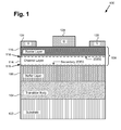
- FIG. 1 shows a cross-sectional view of a conventional high electron mobility transistor (HEMT), depicting its conducting or ON state.
- HEMT 100 includes substrate 102, transition body 104, buffer layer 106, heterostructure 108 including channel layer 114 and overlying barrier layer 116, source electrode 124, drain electrode 126, and gate 128.
- 2DEG two-dimensional electron gas
- 2DEG 118 is generated in heterostructure 108 at or near the interface of channel layer 114 and barrier layer 116 having a larger bandgap than channel layer 114.
- secondary 2DEG 119 which, in some implementations may be undesirably generated at or near the interface of channel layer 114 and buffer layer 106. It is noted that, in some instances, the undesirable conduction channel depicted as secondary 2DEG 119 may in fact take the form of a two-dimensional hole gas (2DHG) of positive charge carriers.
- 2DEG 118 produced by heterostructure 108 can provide a desired, continuous, uninterrupted channel for the flow of current between source electrode 124 and drain electrode 126.
- 2DEG 118 may arise naturally, without the application of a gate potential to gate 126, resulting in HEMT 100 being a normally ON, depletion mode, device.
- buffer layer 106 it may be advantageous or desirable to implement buffer layer 106 using a semiconductor material having a larger bandgap than channel layer 114.
- buffer layer 106 having a larger bandgap than channel layer 114 may reduce the conductivity of buffer layer 106 and provide a barrier for conduction between drain electrode 126 and the layer or layers underlying buffer layer 106, thereby reducing the level of leakage current through HEMT 100.
- undesirable secondary 2DEG 119, or a corresponding undesirable 2DHG appearing as a naturally arising feature at or near the interface of channel layer 114 and buffer layer 106.
- the present application is directed to group III-V heterostructure field-effect transistors (HFETs), such as III-Nitride or other group III-V HEMTs, configured to reduce or substantially suppress formation of an undesirable secondary 2DEG, or an undesirable 2DHG, corresponding to secondary 2DEG 119, in Figure 1 .
- the present inventive concepts include formation of a buffer termination body to mediate the interface of a heterostructure channel layer and an underlying buffer layer having a larger bandgap than the channel layer.
- the buffer termination body is situated between the channel layer and the buffer layer having the larger bandgap, and is formed such that polarization charges at the interface of the channel layer and buffer termination body do not form an effective 2DEG or 2DHG.
- the buffer termination body and underlying buffer layer(s) are configured to have larger bandgaps than the channel layer in order to continue to provide improved punch-through capability and reduced device leakage.
- Figure 2 shows flowchart 200 presenting an exemplary method for forming a group III-V device including a buffer termination body configured to overcome the drawbacks and deficiencies associated with HEMT 100, in Figure 1 .
- Certain details and features have been left out of flowchart 200 that are apparent to a person of ordinary skill in the art in order not to obscure the discussion of the inventive features in the present application.
- Figure 3A shows a cross-sectional view of substrate 310.
- substrate 310 is selected so as to be suitable for use as a support substrate for a group III-V HEMT.
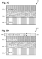
- structures 320, and 330 show the result of forming a transition body (220) and forming an aluminum gallium nitride (AlGaN) buffer layer (230), respectively, over substrate 310.
- Figures 3D , 3F , and 3H show continued formation of the group III-V HEMT having a buffer termination body according to a first exemplary implementation
- Figures 3E , 3G , and 3I show formation of such a device according to a second exemplary implementation.
- Figures 3A through 3I are provided as specific implementations of the present inventive principles, and are shown with such specificity for the purposes of conceptual clarity. It should also be understood that particular details such as the materials used to form the structures shown in Figures 3A through 3I , and the techniques used to produce the various depicted features, are being provided merely as examples, and should not be interpreted as limitations.
- substrate 310 may include any material suitable for use as a substrate for fabrication of a group III-V device.
- substrate 310 may be formed of a group IV material such as silicon (Si), or may be a silicon carbide (SiC) or sapphire substrate.
- substrate 310 may be a native substrate for the materials from which the group III-V device is to be fabricated, such as a native gallium nitride (GaN) or other III-Nitride substrate, for instance.
- GaN native gallium nitride
- substrate 310 is shown as a substantially unitary substrate, in other implementations, substrate 310 may correspond to a silicon on insulator (SOI) substrate, a separation by implantation of oxygen (SIMOX) process substrate, a silicon on sapphire (SOS) substrate, or a single-crystal or polycrystalline SiC on silicon substrate, for example.
- SOI silicon on insulator
- SIMOX separation by implantation of oxygen
- SOS silicon on sapphire
- SiC single-crystal or polycrystalline SiC on silicon substrate
- transition body 322 may be formed over substrate 310 (220).
- substrate 310 is not a native substrate for fabrication of a group III-V HEMT
- transition body 322 may be formed over substrate 310.
- substrate 310 is a silicon substrate
- transition body 322 may correspond to multiple distinguishable layers mediating the lattice transition from substrate 310 to a group III-V material layer.
- transition body 322 may include a nucleation layer (nucleation layer not shown in Figure 3B ), in addition to layers formed so as to reduce the net mismatch in thermal coefficient of expansion between substrate 310 and later formed group III-V active layers.
- a nucleation layer nucleation layer not shown in Figure 3B
- transition body 322 may include an aluminum nitride (AlN) layer formed on substrate 310, or on a stress reducing layer and/or a nucleation layer formed on substrate 310, and may further include a series of AlGaN layers having a progressively reduced aluminum content relative to their gallium content, until a suitable transition to an overlying buffer layer is achieved.
- transition body 322 may take the form of a compositionally graded body having different group III-V alloy compositions at respective top and bottom surfaces.
- Patent Number 6,649,287 entitled “Gallium Nitride Materials and Methods", and issued on November 18, 2003
- U.S. Patent Number 6,617,060 also entitled “Gallium Nitride Materials and Methods", and issued on September 9, 2003
- U.S. Patent Number 7,339,205 entitled “Gallium Nitride Materials and Methods Associated with the Same", and issued on March 4, 2008
- U.S. Patent Application Number 12/928,946 entitled “Stress Modulated Group III-V Semiconductor Device and Related Method", and filed on December 21, 2010
- Patent Application Number 13/397,190 entitled “III-Nitride Heterojunction Devices Having a Multilayer Spacer", and filed on February 15, 2012
- U.S. Patent Application Number 11/531,508 entitled “Process for Manufacture of Super Lattice Using Alternating High and Low Temperature Layers to Block Parasitic Current Path", and filed on September 13, 2006
- U.S. Patent Application Number 13/405,180 entitled “III-Nitride Semiconductor Structures with Strain Absorbing Interlayer Transition Modules", and filed on February 24, 2012.
- AlGaN buffer layer 332 may be formed over transition body 322 (230), as shown by structure 330.
- AlGaN buffer layer 332 may be formed over transition body 322 using any of a number of known growth techniques.
- AlGaN buffer layer may be formed over transition body 322 using molecular-beam epitaxy (MBE), metalorganic chemical vapor deposition (MOCVD), or hydride vapor phase epitaxy (HVPE), to name a few suitable approaches.
- MBE molecular-beam epitaxy
- MOCVD metalorganic chemical vapor deposition
- HVPE hydride vapor phase epitaxy
- AlGaN buffer termination body 342 over AlGaN buffer layer 332 (240), as shown in a first exemplary implementation by structure 340-1.
- AlGaN buffer termination body 342 has bottom surface 343 situated over AlGaN buffer layer 332, top surface 347 opposite bottom surface 343, and thickness 348.
- AlGaN buffer termination body 342 may be formed over AlGaN buffer layer 332 using any of MBE, MOCVD, or HVPE, for example. It is reiterated that AlGaN buffer termination body 342 is represented as an AlGaN body for merely exemplary purposes. More generally, a buffer termination body corresponding to AlGaN buffer termination body 342 may be formed of any suitable III-Nitride or other group III-V material.
- AlGaN buffer termination body 342 may take the form of a single AlGaN layer of substantially uniform composition.
- AlGaN buffer termination body 342 may be formed as a compositionally graded layer, such as a compositionally graded AlGaN or other III-Nitride or group III-V layer having a smaller bandgap at top surface 347 and a larger bandgap at bottom surface 343.
- AlGaN buffer termination body 342 may be formed as a compositionally graded AlGaN layer having a lower aluminum concentration at top surface 347 and a greater aluminum concentration at bottom surface 343.
- structure 340-2 shows formation of AlGaN buffer termination body 342 over AlGaN buffer layer 332 (240), according to a second exemplary implementation.
- a buffer termination body corresponding to AlGaN buffer termination body 342 may include multiple AlGaN or other III-Nitride layers.
- AlGaN buffer termination body 342 may include first AlGaN or other III-Nitride or group III-V layer 344 having a first alloy composition and second AlGaN or other III-Nitride or group III-V layer 346 having a second alloy composition.
- AlGaN buffer termination body 342 may include first AlGaN or other III-Nitride or group III-V layer 344 and second AlGaN or other III-Nitride or group III-V layer 346 situated over first layer 344, wherein a bandgap of first layer 344 is larger than a bandgap of second layer 346.
- first AlGaN layer 344 may have an aluminum concentration that is greater than the aluminum concentration of overlying second AlGaN layer 346.
- impurity graded layers are disclosed in U.S. Patent Number 8,796,738 , entitled “Group III-V Device Structure Having a Selectively Reduced Impurity Concentration", and issued on August 5, 2014. This patent is hereby incorporated fully by reference into the present application.
- flowchart 200 continues with forming GaN based heterostructure 352 including GaN channel layer 354 and AlGaN barrier layer 356 over AlGaN buffer termination body 342 (250), as shown in the first exemplary implementation of structure 350-1.
- heterostructure 352 is configured to produce 2DEG 355 at or near the interface of GaN channel layer 354 and AlGaN barrier layer 356.
- GaN channel layer 354 has thickness 358.
- GaN channel layer 354 and AlGaN barrier layer 356 may be formed using any of MBE, MOCVD, or HVPE, for example.
- AlGaN barrier layer 356 it may be desirable to form AlGaN barrier layer 356 over a spacer layer (or layers) disposed between AlGaN barrier layer 356 and GaN channel layer 354.
- spacer layer(s) examples of using such spacer layer(s) are disclosed in U.S. Patent Number 8,659,030 , entitled “III-Nitride Heterojunction Devices Having a Multilayer Spacer", and issued on February 25, 2014. This patent is hereby incorporated fully by reference into the present application.
- Channel layer 354 and barrier layer 356 are depicted as respective GaN and AlGaN layers for exemplary purposes only. More generally, channel layer 354 and barrier layer 356 can be implemented using any suitable III-Nitride or other group III-V layers for which barrier layer 356 has a bandgap sufficiently larger than the bandgap of channel layer 354 to produce 2DEG 355. In addition, and to reduce or substantially suppress an undesirable secondary 2DEG, or an undesirable 2DHG, from forming in heterostructure 352, buffer termination body 342 is situated between buffer layer 332 and channel layer 354, and has a bandgap smaller than the bandgap of buffer layer 332 and larger than the bandgap of channel layer 354.
- buffer layer 332 may be implemented as an AlGaN buffer layer having an aluminum concentration of approximately four percent (4%), or greater.
- buffer termination body 342 may be a compositionally graded AlGaN layer having an aluminum concentration of approximately 1% or less at top surface 347 and an aluminum concentration of from approximately 2% to approximately 4% at bottom surface 343.
- the expression “substantially suppress an undesirable secondary 2DEG” refers to the fact although a secondary 2DEG, or a 2DHG, may appear at or near the interface of channel layer 354 and buffer termination body 342, that secondary 2DEG, or 2DHG, is not an effective conduction channel. That is to say, the available density of charge carrier states that could be filled at or near the interface of channel layer 354 and buffer termination body 342 is less than approximately 10% of the available density of electron states formed in desirable 2DEG 355. As a result, that weak (or ineffective) secondary 2DEG, or 2DHG, has negligible affect on the performance of the resulting HEMT, and is therefore characterized as being substantially suppressed.
- AlGaN buffer termination body 342 may include multiple AlGaN layers having different aluminum concentrations.
- channel layer 354 takes the form of a GaN channel layer including substantially no aluminum
- buffer layer 332 is implemented as an AlGaN buffer layer having an aluminum concentration of approximately 4%, or greater
- first AlGaN layer 344 may have an aluminum concentration of approximately 2%, or between approximately 2% and approximately 4%
- second AlGaN layer 346 may have an aluminum concentration of approximately 1% or less.
- buffer termination body 342 may be advantageous or desirable to form buffer termination body 342 of either or both of structures 350-1 and 350-2 so as to have a thin sharp grade.
- buffer termination body 342 and channel layer 354 may be formed such that thickness 348 of buffer termination body 342 is less than or approximately equal to thickness 358 of channel layer 354.
- the sum of thickness 348 and thickness 358 may be expected to be sufficiently thin to be punch-through resistant.
- buffer termination body 342 can be configured such that it reduces or substantially suppresses the undesirable formation of a secondary 2DEG at or near its interface with channel layer 354, while concurrently providing improved punch-through capability and reduced device leakage.
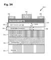
- Source electrode 364 and drain electrode 366 may be formed of any suitable conductive material, and are formed so as to make ohmic contact with heterojunction 352.
- Gate 368 may be implemented as a Schottky gate making Schottky contact with barrier layer 356, or as an insulated gate including a gate dielectric (gate dielectric not shown in Figures 3H and 3I ) and being capacitively coupled to barrier layer 356.
- the resulting HEMT corresponding to either or both of structures 360-1 and 360-2 may be implemented as a midvoltage or high voltage device, as defined above in the Definition section of the present application.
- the present application discloses group III-V HEMTs configured to reduce or substantially suppress formation of an undesirable secondary 2DEG.
- reduction or substantial suppression is achieved by situating a buffer termination body having a bandgap larger than that of a channel layer and smaller than that of a buffer layer, between the channel layer and the buffer layer.
- the buffer termination body is configured to have a larger bandgap than the channel layer in order to continue to provide improved punch-through capability and reduced device leakage.
Landscapes
- Junction Field-Effect Transistors (AREA)
Abstract
Description
- The present application claims the benefit of and priority to a provisional application entitled "Compositionally Graded HEMT Buffer Termination," Serial No.
61/897,525 filed on October 30, 2013 - As used herein, "III-Nitride" or "III-N" refers to a compound semiconductor that includes nitrogen and at least one group III element such as aluminum (Al), gallium (Ga), indium (In), and boron (B), and including but not limited to any of its alloys, such as aluminum gallium nitride (AlxGa(1-x)N), indium gallium nitride (InyGa(1-y)N), aluminum indium gallium nitride (AlxInyGa(1-x-y)N), gallium arsenide phosphide nitride (GaAsaPbN(1-a-b)), aluminum indium gallium arsenide phosphide nitride (AlxInyGa(1-x-y)AsaPbN(1-a-b)), for example. III-N also refers generally to any polarity including but not limited to Ga-polar, N-polar, semi-polar, or non-polar crystal orientations. A III-N material may also include either the Wurtzitic, Zincblende, or mixed polytypes, and may include single-crystal, monocrystalline, polycrystalline, or amorphous structures. Gallium nitride or GaN, as used herein, refers to a III-N compound semiconductor wherein the group III element or elements include some or a substantial amount of gallium, but may also include other group III elements in addition to gallium. A III-N or a GaN transistor may also refer to a composite high voltage enhancement mode transistor that is formed by connecting the III-N or the GaN transistor in cascode with a lower voltage group IV transistor.
- In addition, as used herein, the phrase "group IV" refers to a semiconductor that includes at least one group IV element such as silicon (Si), germanium (Ge), and carbon (C), and may also include compound semiconductors such as silicon germanium (SiGe) and silicon carbide (SiC), for example. Group IV also refers to semiconductor materials which include more than one layer of group IV elements, or doping of group IV elements to produce strained group IV materials, and may also include group IV based composite substrates such as single-crystal or polycrystalline SiC on silicon, silicon on insulator (SOI), separation by implantation of oxygen (SIMOX) process substrates, and silicon on sapphire (SOS), for example.
- It is noted that, as used herein, the terms "low voltage" or "LV" in reference to a transistor or switch describes a transistor or switch with a voltage range of up to approximately fifty volts (50V). It is further noted that use of the term "midvoltage" or "MV" refers to a voltage range from approximately fifty volts to approximately two hundred volts (approximately 50V to 200V). Moreover, the term "high voltage" or "HV," as used herein, refers to a voltage range from approximately two hundred volts to approximately twelve hundred volts (approximately 200V to 1200V), or higher.
- Group III-V heterostructure field-effect transistors (HFETs), such as gallium nitride (GaN) or other III-Nitride based high mobility electron transistors (HEMTs), may be desirable for use in high power and high performance circuit applications due to their high efficiency and high-voltage capability. III-Nitride and other group III-V HEMTs operate using polarization fields to generate a two-dimensional electron gas (2DEG) allowing for high current densities with low resistive losses. Because the 2DEG can arise naturally near the interface of a III-Nitride channel layer and an overlying III-Nitride barrier layer having a larger bandgap than the channel layer, III-Nitride HEMTS typically conduct without the application of a gate potential.
- In some implementations, it may be advantageous or desirable to implement a buffer layer underlying the III-Nitride channel and barrier layers using a III-Nitride material also having a larger bandgap than the channel layer. For example, use of a larger bandgap buffer layer under the channel layer may reduce the conductivity of the buffer layer, thereby reducing leakage current through the HEMT. However, such an implementation may undesirably result in a naturally arising secondary 2DEG at the interface of the channel layer and the underlying buffer layer having the larger bandgap.
- The present disclosure is directed to a group III-V device including a buffer termination body, substantially as shown in and/or described in connection with at least one of the figures, and as set forth more completely in the claims.
-
-
Figure 1 shows a cross-sectional view of a conventional group III-V high electron mobility transistor (HEMT), depicting its ON state. -
Figure 2 shows a flowchart presenting an exemplary method for forming a group III-V device including a buffer termination body, according to one implementation. -
Figure 3A shows a cross-sectional view of a structure corresponding to an initial formation stage, according to one implementation of the flowchart ofFigure 2 . -
Figure 3B shows a cross-sectional view of the structure ofFigure 3A at a subsequent formation stage, according to one implementation of the flowchart ofFigure 2 . -
Figure 3C shows a cross-sectional view of the structure ofFigure 3B at a subsequent formation stage, according to one implementation of the flowchart ofFigure 2 . -
Figure 3D shows a cross-sectional view of the structure ofFigure 3C at a subsequent formation stage, according to a first exemplary implementation of the flowchart ofFigure 2 . -
Figure 3E shows a cross-sectional view of the structure ofFigure 3C at a subsequent formation stage, according to a second exemplary implementation of the flowchart ofFigure 2 . -
Figure 3F shows a cross-sectional view of the structure ofFigure 3D at a subsequent formation stage, according to the first exemplary implementation of the flowchart ofFigure 2 . -
Figure 3G shows a cross-sectional view of the structure ofFigure 3E at a subsequent formation stage, according to the second exemplary implementation of the flowchart ofFigure 2 . -
Figure 3H shows a cross-sectional view of the structure ofFigure 3F at a subsequent formation stage, according to the first exemplary implementation of the flowchart ofFigure 2 . -
Figure 3I shows a cross-sectional view of the structure ofFigure 3G at a subsequent formation stage, according to the second exemplary implementation of the flowchart ofFigure 2 . - The following description contains specific information pertaining to implementations in the present disclosure. One skilled in the art will recognize that the present disclosure may be implemented in a manner different from that specifically discussed herein. The drawings in the present application and their accompanying detailed description are directed to merely exemplary implementations. Unless noted otherwise, like or corresponding elements among the figures may be indicated by like or corresponding reference numerals. Moreover, the drawings and illustrations in the present application are generally not to scale, and are not intended to correspond to actual relative dimensions.
-
Figure 1 shows a cross-sectional view of a conventional high electron mobility transistor (HEMT), depicting its conducting or ON state. HEMT 100 includessubstrate 102,transition body 104,buffer layer 106,heterostructure 108 includingchannel layer 114 and overlyingbarrier layer 116,source electrode 124,drain electrode 126, andgate 128. As shown inFigure 1 , in its ON state, HEMT 100 includes two-dimensional electron gas (2DEG) 118 providing a desired conduction channel for the charge carriers of HEMT 100 betweensource electrode 124 anddrain electrode 126, which are ohmic contacts. As further shown inFigure 1 ,2DEG 118 is generated inheterostructure 108 at or near the interface ofchannel layer 114 andbarrier layer 116 having a larger bandgap thanchannel layer 114. Also shown inFigure 1 issecondary 2DEG 119, which, in some implementations may be undesirably generated at or near the interface ofchannel layer 114 andbuffer layer 106. It is noted that, in some instances, the undesirable conduction channel depicted assecondary 2DEG 119 may in fact take the form of a two-dimensional hole gas (2DHG) of positive charge carriers. - As illustrated by
Figure 1 , 2DEG 118 produced byheterostructure 108 can provide a desired, continuous, uninterrupted channel for the flow of current betweensource electrode 124 anddrain electrode 126. As known in the art,2DEG 118 may arise naturally, without the application of a gate potential togate 126, resulting in HEMT 100 being a normally ON, depletion mode, device. Moreover, and as noted above, in some implementations, it may be advantageous or desirable to implementbuffer layer 106 using a semiconductor material having a larger bandgap thanchannel layer 114. For example, and as further noted above, use ofbuffer layer 106 having a larger bandgap thanchannel layer 114 may reduce the conductivity ofbuffer layer 106 and provide a barrier for conduction betweendrain electrode 126 and the layer or layers underlyingbuffer layer 106, thereby reducing the level of leakage current through HEMT 100. However, such an implementation may result in undesirablesecondary 2DEG 119, or a corresponding undesirable 2DHG, appearing as a naturally arising feature at or near the interface ofchannel layer 114 andbuffer layer 106. - The present application is directed to group III-V heterostructure field-effect transistors (HFETs), such as III-Nitride or other group III-V HEMTs, configured to reduce or substantially suppress formation of an undesirable secondary 2DEG, or an undesirable 2DHG, corresponding to
secondary 2DEG 119, inFigure 1 . The present inventive concepts include formation of a buffer termination body to mediate the interface of a heterostructure channel layer and an underlying buffer layer having a larger bandgap than the channel layer. The buffer termination body is situated between the channel layer and the buffer layer having the larger bandgap, and is formed such that polarization charges at the interface of the channel layer and buffer termination body do not form an effective 2DEG or 2DHG. Moreover, the buffer termination body and underlying buffer layer(s) are configured to have larger bandgaps than the channel layer in order to continue to provide improved punch-through capability and reduced device leakage. - Referring to
Figure 2, Figure 2 showsflowchart 200 presenting an exemplary method for forming a group III-V device including a buffer termination body configured to overcome the drawbacks and deficiencies associated withHEMT 100, inFigure 1 . Certain details and features have been left out offlowchart 200 that are apparent to a person of ordinary skill in the art in order not to obscure the discussion of the inventive features in the present application. - Referring now to
Figure 3A, Figure 3A shows a cross-sectional view ofsubstrate 310. In particular,substrate 310 is selected so as to be suitable for use as a support substrate for a group III-V HEMT. Proceeding on toFigures 3B and3C ,structures substrate 310. Moreover,Figures 3D ,3F , and3H show continued formation of the group III-V HEMT having a buffer termination body according to a first exemplary implementation, whileFigures 3E ,3G , and3I show formation of such a device according to a second exemplary implementation. - It is noted that the structures shown in
Figures 3A, 3B ,3C, 3D ,3E ,3F ,3G ,3H , and3I (hereinafter "Figures 3A through 3I ") are provided as specific implementations of the present inventive principles, and are shown with such specificity for the purposes of conceptual clarity. It should also be understood that particular details such as the materials used to form the structures shown inFigures 3A through 3I , and the techniques used to produce the various depicted features, are being provided merely as examples, and should not be interpreted as limitations. - Referring to
Figure 3A in conjunction withFigure 2 ,flowchart 200 begins with providingsubstrate 310 for fabrication of a III-Nitride or other group III-V device (210).Substrate 310 may include any material suitable for use as a substrate for fabrication of a group III-V device. For example,substrate 310 may be formed of a group IV material such as silicon (Si), or may be a silicon carbide (SiC) or sapphire substrate. Alternatively, in some implementations,substrate 310 may be a native substrate for the materials from which the group III-V device is to be fabricated, such as a native gallium nitride (GaN) or other III-Nitride substrate, for instance. Moreover, althoughsubstrate 310 is shown as a substantially unitary substrate, in other implementations,substrate 310 may correspond to a silicon on insulator (SOI) substrate, a separation by implantation of oxygen (SIMOX) process substrate, a silicon on sapphire (SOS) substrate, or a single-crystal or polycrystalline SiC on silicon substrate, for example. - Turning to
Figure 3B with further reference toFigure 2 ,flowchart 200 continues with formingtransition body 322 over substrate 310 (220). As shown bystructure 320 inFigure 3B , in implementations in whichsubstrate 310 is not a native substrate for fabrication of a group III-V HEMT,transition body 322 may be formed oversubstrate 310. As a specific example, wheresubstrate 310 is a silicon substrate,transition body 322 may correspond to multiple distinguishable layers mediating the lattice transition fromsubstrate 310 to a group III-V material layer. - In one implementation,
transition body 322 may include a nucleation layer (nucleation layer not shown inFigure 3B ), in addition to layers formed so as to reduce the net mismatch in thermal coefficient of expansion betweensubstrate 310 and later formed group III-V active layers. For instance, when forming a GaN based HEMT,transition body 322 may include an aluminum nitride (AlN) layer formed onsubstrate 310, or on a stress reducing layer and/or a nucleation layer formed onsubstrate 310, and may further include a series of AlGaN layers having a progressively reduced aluminum content relative to their gallium content, until a suitable transition to an overlying buffer layer is achieved. Moreover, in some implementations,transition body 322 may take the form of a compositionally graded body having different group III-V alloy compositions at respective top and bottom surfaces. - Examples of using a compositionally graded transition body, as well as use of intermediate layers, stress reducing layers, and various interlayers are disclosed in U.S.
- Patent Number
6,649,287 , entitled "Gallium Nitride Materials and Methods", and issued on November 18, 2003;U.S. Patent Number 6,617,060 , also entitled "Gallium Nitride Materials and Methods", and issued on September 9, 2003;U.S. Patent Number 7,339,205 , entitled "Gallium Nitride Materials and Methods Associated with the Same", and issued on March 4, 2008;U.S. Patent Application Number 12/928,946 U.S. Patent Application Number 13/397,190 U.S. Patent Application Number 11/531,508 U.S. Patent Application Number 13/405,180 - Moving to
Figure 3C with further reference toFigure 2 ,flowchart 200 continues with formingAlGaN buffer layer 332 over transition body 322 (230), as shown bystructure 330.AlGaN buffer layer 332 may be formed overtransition body 322 using any of a number of known growth techniques. For example, AlGaN buffer layer may be formed overtransition body 322 using molecular-beam epitaxy (MBE), metalorganic chemical vapor deposition (MOCVD), or hydride vapor phase epitaxy (HVPE), to name a few suitable approaches. - Continuing to
Figure 3D ,flowchart 200 continues with forming AlGaNbuffer termination body 342 over AlGaN buffer layer 332 (240), as shown in a first exemplary implementation by structure 340-1. As shown inFigure 3D , AlGaNbuffer termination body 342 hasbottom surface 343 situated overAlGaN buffer layer 332,top surface 347 oppositebottom surface 343, andthickness 348. AlGaNbuffer termination body 342 may be formed overAlGaN buffer layer 332 using any of MBE, MOCVD, or HVPE, for example. It is reiterated that AlGaNbuffer termination body 342 is represented as an AlGaN body for merely exemplary purposes. More generally, a buffer termination body corresponding to AlGaNbuffer termination body 342 may be formed of any suitable III-Nitride or other group III-V material. - In one implementation, AlGaN
buffer termination body 342 may take the form of a single AlGaN layer of substantially uniform composition. However, in other implementations, AlGaNbuffer termination body 342 may be formed as a compositionally graded layer, such as a compositionally graded AlGaN or other III-Nitride or group III-V layer having a smaller bandgap attop surface 347 and a larger bandgap atbottom surface 343. For example, in implementations in which the buffer termination body is formed of AlGaN, as depicted inFigure 3D , AlGaNbuffer termination body 342 may be formed as a compositionally graded AlGaN layer having a lower aluminum concentration attop surface 347 and a greater aluminum concentration atbottom surface 343. - Referring to
Figure 3E , structure 340-2 shows formation of AlGaNbuffer termination body 342 over AlGaN buffer layer 332 (240), according to a second exemplary implementation. As shown inFigure 3E , a buffer termination body corresponding to AlGaNbuffer termination body 342 may include multiple AlGaN or other III-Nitride layers. For example, AlGaNbuffer termination body 342 may include first AlGaN or other III-Nitride or group III-V layer 344 having a first alloy composition and second AlGaN or other III-Nitride or group III-V layer 346 having a second alloy composition. - In some implementations, as shown in
Figure 3E , AlGaNbuffer termination body 342 may include first AlGaN or other III-Nitride or group III-V layer 344 and second AlGaN or other III-Nitride or group III-V layer 346 situated overfirst layer 344, wherein a bandgap offirst layer 344 is larger than a bandgap ofsecond layer 346. For example, in implementations in which a buffer termination body corresponding to buffertermination body 342 is formed of AlGaN, as depicted inFigure 3E ,first AlGaN layer 344 may have an aluminum concentration that is greater than the aluminum concentration of overlyingsecond AlGaN layer 346. - In some implementations, it may be advantageous or desirable to include one or more impurity graded layers in AlGaN
buffer termination body 342 of either or both of structures 340-1 and 340-2 and/or AlGaN buffer layer(s) 332. Examples of impurity graded layers are disclosed inU.S. Patent Number 8,796,738 , entitled "Group III-V Device Structure Having a Selectively Reduced Impurity Concentration", and issued on August 5, 2014. This patent is hereby incorporated fully by reference into the present application. - Moving to
Figure 3F ,flowchart 200 continues with forming GaN basedheterostructure 352 includingGaN channel layer 354 andAlGaN barrier layer 356 over AlGaN buffer termination body 342 (250), as shown in the first exemplary implementation of structure 350-1. As shown inFigure 3F , heterostructure 352 is configured to produce2DEG 355 at or near the interface ofGaN channel layer 354 andAlGaN barrier layer 356. As further shown inFigure 3F ,GaN channel layer 354 hasthickness 358.GaN channel layer 354 andAlGaN barrier layer 356 may be formed using any of MBE, MOCVD, or HVPE, for example. - It is noted that in certain implementations, it may be desirable to form
AlGaN barrier layer 356 over a spacer layer (or layers) disposed betweenAlGaN barrier layer 356 andGaN channel layer 354. Examples of using such spacer layer(s) are disclosed inU.S. Patent Number 8,659,030 , entitled "III-Nitride Heterojunction Devices Having a Multilayer Spacer", and issued on February 25, 2014. This patent is hereby incorporated fully by reference into the present application. Moreover, in some implementations, it may be advantageous or desirable to use a thin layer of AlN or high Al content AlGaN in conjunction withAlGaN barrier layer 356 to aid in confinement of2DEG 355. -
Channel layer 354 andbarrier layer 356 are depicted as respective GaN and AlGaN layers for exemplary purposes only. More generally,channel layer 354 andbarrier layer 356 can be implemented using any suitable III-Nitride or other group III-V layers for whichbarrier layer 356 has a bandgap sufficiently larger than the bandgap ofchannel layer 354 to produce2DEG 355. In addition, and to reduce or substantially suppress an undesirable secondary 2DEG, or an undesirable 2DHG, from forming inheterostructure 352,buffer termination body 342 is situated betweenbuffer layer 332 andchannel layer 354, and has a bandgap smaller than the bandgap ofbuffer layer 332 and larger than the bandgap ofchannel layer 354. - For example, in implementations in which
channel layer 354 takes the form of a GaN channel layer including substantially no aluminum, leakage inbuffer layer 332 may be advantageously reduced whenbuffer layer 332 is implemented as an AlGaN buffer layer having an aluminum concentration of approximately four percent (4%), or greater. In such an implementation,buffer termination body 342 may be a compositionally graded AlGaN layer having an aluminum concentration of approximately 1% or less attop surface 347 and an aluminum concentration of from approximately 2% to approximately 4% atbottom surface 343. - It is noted that, as used herein, the expression "substantially suppress an undesirable secondary 2DEG" refers to the fact although a secondary 2DEG, or a 2DHG, may appear at or near the interface of
channel layer 354 andbuffer termination body 342, that secondary 2DEG, or 2DHG, is not an effective conduction channel. That is to say, the available density of charge carrier states that could be filled at or near the interface ofchannel layer 354 andbuffer termination body 342 is less than approximately 10% of the available density of electron states formed indesirable 2DEG 355. As a result, that weak (or ineffective) secondary 2DEG, or 2DHG, has negligible affect on the performance of the resulting HEMT, and is therefore characterized as being substantially suppressed. - Referring to
Figure 3G , structure 350-2 shows formation of GaN basedheterostructure 352 over AlGaN buffer termination body 342 (250), according to the second exemplary implementation. As shown inFigure 3G , AlGaNbuffer termination body 342 may include multiple AlGaN layers having different aluminum concentrations. For example, in implementations in whichchannel layer 354 takes the form of a GaN channel layer including substantially no aluminum, as described above, andbuffer layer 332 is implemented as an AlGaN buffer layer having an aluminum concentration of approximately 4%, or greater,first AlGaN layer 344 may have an aluminum concentration of approximately 2%, or between approximately 2% and approximately 4%, whilesecond AlGaN layer 346 may have an aluminum concentration of approximately 1% or less. - In some implementations, it may be advantageous or desirable to form
buffer termination body 342 of either or both of structures 350-1 and 350-2 so as to have a thin sharp grade. For example,buffer termination body 342 andchannel layer 354 may be formed such thatthickness 348 ofbuffer termination body 342 is less than or approximately equal tothickness 358 ofchannel layer 354. In such implementations, the sum ofthickness 348 andthickness 358 may be expected to be sufficiently thin to be punch-through resistant. Thus,buffer termination body 342 can be configured such that it reduces or substantially suppresses the undesirable formation of a secondary 2DEG at or near its interface withchannel layer 354, while concurrently providing improved punch-through capability and reduced device leakage. - Moving to
Figure 3H andFigure 3I ,flowchart 200 concludes with formingsource electrode 364,drain electrode 366, andgate 368 over heterostructure 352 (260), as shown in the first and second exemplary implementations of respective structures 360-1 and 360-2.Source electrode 364 anddrain electrode 366 may be formed of any suitable conductive material, and are formed so as to make ohmic contact withheterojunction 352.Gate 368 may be implemented as a Schottky gate making Schottky contact withbarrier layer 356, or as an insulated gate including a gate dielectric (gate dielectric not shown inFigures 3H and3I ) and being capacitively coupled tobarrier layer 356. The resulting HEMT corresponding to either or both of structures 360-1 and 360-2 may be implemented as a midvoltage or high voltage device, as defined above in the Definition section of the present application. - Thus, the present application discloses group III-V HEMTs configured to reduce or substantially suppress formation of an undesirable secondary 2DEG. Such reduction or substantial suppression is achieved by situating a buffer termination body having a bandgap larger than that of a channel layer and smaller than that of a buffer layer, between the channel layer and the buffer layer. As a result, the polarization charges at the interface of the channel layer and buffer termination body do not form an effective secondary 2DEG. Moreover, the buffer termination body is configured to have a larger bandgap than the channel layer in order to continue to provide improved punch-through capability and reduced device leakage.
- From the above description it is manifest that various techniques can be used for implementing the concepts described in the present application without departing from the scope of those concepts. Moreover, while the concepts have been described with specific reference to certain implementations, a person of ordinary skill in the art would recognize that changes can be made in form and detail without departing from the scope of those concepts. As such, the described implementations are to be considered in all respects as illustrative and not restrictive. It should also be understood that the present application is not limited to the particular implementations described herein, but many rearrangements, modifications, and substitutions are possible without departing from the scope of the present disclosure.
Claims (15)
- A III-Nitride device comprising:a III-Nitride buffer layer situated over a substrate, said III-Nitride buffer layer having a first bandgap;a III-Nitride heterostructure situated over said III-Nitride buffer layer and configured to produce a two-dimensional electron gas (2DEG), said III-Nitride heterostructure including a channel layer having a second bandgap smaller than said first bandgap;a buffer termination body situated between said III-Nitride buffer layer and said channel layer, said buffer termination body comprising a III-Nitride material having a third bandgap smaller than said first bandgap and larger than said second bandgap.
- The III-Nitride device of claim 1, wherein said buffer termination body comprises a compositionally graded III-Nitride layer.
- The III-Nitride device of claim 1, wherein said buffer termination body comprises a compositionally graded III-Nitride layer having a smaller bandgap at a top surface and a larger bandgap at a bottom surface.
- The III-Nitride device of claim 1, wherein said buffer termination body comprises at least a first III-Nitride layer having a first III-Nitride composition and a second III-Nitride layer having a second III-Nitride composition.
- The III-Nitride device of claim 1, wherein said buffer termination body comprises at least a first III-Nitride layer and a second III-Nitride layer situated over said first III-Nitride layer, wherein a bandgap of said first III-Nitride layer is larger than a bandgap of said second III-Nitride layer.
- The III-Nitride device of claim 1, wherein a thickness of said buffer termination body is less than or approximately equal to a thickness of said channel layer.
- The III-Nitride device of claim 1, wherein said III-Nitride buffer layer and said buffer termination body comprise aluminum gallium nitride (AlGaN).
- A III-Nitride device comprising:a III-Nitride buffer layer formed over a substrate, said III-Nitride buffer layer having a first aluminum concentration;a III-Nitride heterostructure situated over said III-Nitride buffer layer and configured to produce a two-dimensional electron gas (2DEG), said III-Nitride heterostructure including a channel layer comprising substantially no aluminum;a buffer termination body situated between said III-Nitride buffer layer and said channel layer, said buffer termination body comprising aluminum and having a second aluminum concentration less than said first aluminum concentration.
- The III-Nitride device of claim 8, wherein said buffer termination body comprises a compositionally graded III-Nitride layer.
- The III-Nitride device of claim 8, wherein said buffer termination body comprises a compositionally graded III-Nitride layer having a lower aluminum concentration at a top surface and a greater aluminum concentration at a bottom surface.
- The III-Nitride device of claim 8, wherein said buffer termination body comprises at least a first III-Nitride layer having a first III-Nitride composition and a second III-Nitride layer having a second III-Nitride composition.
- The III-Nitride device of claim 8, wherein said buffer termination body comprises at least a first III-Nitride layer and a second III-Nitride layer situated over said first III-Nitride layer, wherein an aluminum concentration of said first III-Nitride layer is greater than an aluminum concentration of said second III-Nitride layer.
- The III-Nitride device of claim 8, wherein a thickness of said buffer termination body is less than or approximately equal to a thickness of said channel layer.
- The III-Nitride device of claim 8, wherein said III-Nitride buffer layer and said buffer termination body comprise aluminum gallium nitride (AlGaN).
- A method of forming a III-Nitride device, said method comprising:forming a III-Nitride buffer layer having a first bandgap over a substrate;forming a buffer termination body over said III-Nitride buffer layer;forming a III-Nitride heterostructure over said buffer termination body, said III-Nitride heterostructure configured to produce a two-dimensional electron gas (2DEG), said III-Nitride heterostructure including a channel layer having a second bandgap smaller than said first bandgap;wherein said buffer termination body has a third bandgap smaller than said first bandgap and larger than said second bandgap.
Applications Claiming Priority (2)
| Application Number | Priority Date | Filing Date | Title |
|---|---|---|---|
| US201361897525P | 2013-10-30 | 2013-10-30 | |
| US14/505,252 US20150115327A1 (en) | 2013-10-30 | 2014-10-02 | Group III-V Device Including a Buffer Termination Body |
Publications (1)
| Publication Number | Publication Date |
|---|---|
| EP2869347A1 true EP2869347A1 (en) | 2015-05-06 |
Family
ID=51730415
Family Applications (1)
| Application Number | Title | Priority Date | Filing Date |
|---|---|---|---|
| EP20140189359 Ceased EP2869347A1 (en) | 2013-10-30 | 2014-10-17 | Group III-V device including a buffer termination body |
Country Status (2)
| Country | Link |
|---|---|
| US (1) | US20150115327A1 (en) |
| EP (1) | EP2869347A1 (en) |
Cited By (1)
| Publication number | Priority date | Publication date | Assignee | Title |
|---|---|---|---|---|
| EP3321968A1 (en) * | 2016-11-15 | 2018-05-16 | Infineon Technologies Austria AG | High electron mobility transistor with graded back-barrier region |
Families Citing this family (8)
| Publication number | Priority date | Publication date | Assignee | Title |
|---|---|---|---|---|
| JP5781292B2 (en) * | 2010-11-16 | 2015-09-16 | ローム株式会社 | Nitride semiconductor device and nitride semiconductor package |
| WO2017071635A1 (en) * | 2015-10-30 | 2017-05-04 | The Hong Kong University Of Science And Technology | Semiconductor device with iii-nitride channel region and silicon carbide drift region |
| US11094814B2 (en) * | 2017-09-29 | 2021-08-17 | Epistar Corporation | Semiconductor power device |
| US11515407B2 (en) * | 2018-12-26 | 2022-11-29 | Intel Corporation | High breakdown voltage structure for high performance GaN-based HEMT and MOS devices to enable GaN C-MOS |
| CN111739960B (en) * | 2020-05-14 | 2022-07-26 | 中山大学 | Gain type heterojunction ultraviolet photoelectric detector |
| US11515397B2 (en) * | 2020-07-21 | 2022-11-29 | Globalfoundries U.S. Inc. | III-V compound semiconductor layer stacks with electrical isolation provided by a trap-rich layer |
| US12027615B2 (en) | 2020-12-18 | 2024-07-02 | Innoscience (Suzhou) Technology Co., Ltd. | Semiconductor device and method for manufacturing the same |
| CN113130644B (en) * | 2020-12-18 | 2023-03-24 | 英诺赛科(苏州)科技有限公司 | Semiconductor device and method of manufacturing semiconductor device |
Citations (5)
| Publication number | Priority date | Publication date | Assignee | Title |
|---|---|---|---|---|
| US6617060B2 (en) | 2000-12-14 | 2003-09-09 | Nitronex Corporation | Gallium nitride materials and methods |
| US7339205B2 (en) | 2004-06-28 | 2008-03-04 | Nitronex Corporation | Gallium nitride materials and methods associated with the same |
| US20110073911A1 (en) * | 2009-09-26 | 2011-03-31 | Sanken Electric Co., Ltd. | Semiconductor device |
| US8659030B2 (en) | 2011-02-28 | 2014-02-25 | International Rectifier Corporation | III-nitride heterojunction devices having a multilayer spacer |
| US8796738B2 (en) | 2011-09-21 | 2014-08-05 | International Rectifier Corporation | Group III-V device structure having a selectively reduced impurity concentration |
Family Cites Families (15)
| Publication number | Priority date | Publication date | Assignee | Title |
|---|---|---|---|---|
| JP3393602B2 (en) * | 2000-01-13 | 2003-04-07 | 松下電器産業株式会社 | Semiconductor device |
| US7098490B2 (en) * | 2003-06-02 | 2006-08-29 | Hrl Laboratories, Llc | GaN DHFET |
| US8853666B2 (en) * | 2005-12-28 | 2014-10-07 | Renesas Electronics Corporation | Field effect transistor, and multilayered epitaxial film for use in preparation of field effect transistor |
| KR100756841B1 (en) * | 2006-03-13 | 2007-09-07 | 서울옵토디바이스주식회사 | Light Emitting Diode Having Al-An-Bn Buffer Layer And Method Of Manufacturing The Same |
| JP4592742B2 (en) * | 2007-12-27 | 2010-12-08 | Dowaエレクトロニクス株式会社 | Semiconductor material, method for manufacturing semiconductor material, and semiconductor element |
| US8159004B2 (en) * | 2008-08-26 | 2012-04-17 | Sanken Electric Co., Ltd. | Compound semiconductor device having dopant concentration gradient |
| US8748244B1 (en) * | 2010-01-13 | 2014-06-10 | Hrl Laboratories, Llc | Enhancement and depletion mode GaN HMETs on the same substrate |
| KR101774933B1 (en) * | 2010-03-02 | 2017-09-06 | 삼성전자 주식회사 | High Electron Mobility Transistor representing dual depletion and method of manufacturing the same |
| US8686473B1 (en) * | 2010-06-02 | 2014-04-01 | Hrl Laboratories, Llc | Apparatus and method for reducing the interface resistance in GaN heterojunction FETs |
| JP5781292B2 (en) * | 2010-11-16 | 2015-09-16 | ローム株式会社 | Nitride semiconductor device and nitride semiconductor package |
| JP5665676B2 (en) * | 2011-07-11 | 2015-02-04 | Dowaエレクトロニクス株式会社 | Group III nitride epitaxial substrate and manufacturing method thereof |
| US9165766B2 (en) * | 2012-02-03 | 2015-10-20 | Transphorm Inc. | Buffer layer structures suited for III-nitride devices with foreign substrates |
| US8860091B2 (en) * | 2012-04-16 | 2014-10-14 | Hrl Laboratories, Llc | Group III-N HFET with a graded barrier layer |
| JP5421442B1 (en) * | 2012-09-26 | 2014-02-19 | 株式会社東芝 | Nitride semiconductor wafer, nitride semiconductor device, and method of manufacturing nitride semiconductor wafer |
| JP6119165B2 (en) * | 2012-09-28 | 2017-04-26 | 富士通株式会社 | Semiconductor device |
-
2014
- 2014-10-02 US US14/505,252 patent/US20150115327A1/en not_active Abandoned
- 2014-10-17 EP EP20140189359 patent/EP2869347A1/en not_active Ceased
Patent Citations (6)
| Publication number | Priority date | Publication date | Assignee | Title |
|---|---|---|---|---|
| US6617060B2 (en) | 2000-12-14 | 2003-09-09 | Nitronex Corporation | Gallium nitride materials and methods |
| US6649287B2 (en) | 2000-12-14 | 2003-11-18 | Nitronex Corporation | Gallium nitride materials and methods |
| US7339205B2 (en) | 2004-06-28 | 2008-03-04 | Nitronex Corporation | Gallium nitride materials and methods associated with the same |
| US20110073911A1 (en) * | 2009-09-26 | 2011-03-31 | Sanken Electric Co., Ltd. | Semiconductor device |
| US8659030B2 (en) | 2011-02-28 | 2014-02-25 | International Rectifier Corporation | III-nitride heterojunction devices having a multilayer spacer |
| US8796738B2 (en) | 2011-09-21 | 2014-08-05 | International Rectifier Corporation | Group III-V device structure having a selectively reduced impurity concentration |
Non-Patent Citations (1)
| Title |
|---|
| PENG ENCHAO ET AL: "Bipolar characteristics of AlGaN/AlN/GaN/AlGaN double heterojunction structure with AlGaN as buffer layer", JOURNAL OF ALLOYS AND COMPOUNDS, vol. 576, 22 April 2013 (2013-04-22), pages 48 - 53, XP028681940, ISSN: 0925-8388, DOI: 10.1016/J.JALLCOM.2013.04.085 * |
Cited By (2)
| Publication number | Priority date | Publication date | Assignee | Title |
|---|---|---|---|---|
| EP3321968A1 (en) * | 2016-11-15 | 2018-05-16 | Infineon Technologies Austria AG | High electron mobility transistor with graded back-barrier region |
| US10636899B2 (en) | 2016-11-15 | 2020-04-28 | Infineon Technologies Austria Ag | High electron mobility transistor with graded back-barrier region |
Also Published As
| Publication number | Publication date |
|---|---|
| US20150115327A1 (en) | 2015-04-30 |
Similar Documents
| Publication | Publication Date | Title |
|---|---|---|
| US9837522B2 (en) | III-nitride bidirectional device | |
| US9343562B2 (en) | Dual-gated group III-V merged transistor | |
| US20150115327A1 (en) | Group III-V Device Including a Buffer Termination Body | |
| US9196614B2 (en) | Inverted III-nitride P-channel field effect transistor with hole carriers in the channel | |
| US10211329B2 (en) | Charge trapping prevention III-Nitride transistor | |
| US10109728B2 (en) | Transistor structure including a scandium gallium nitride back-barrier layer | |
| KR101809329B1 (en) | Seed layer structure for growth of iii-v materials on silicon | |
| US20180097072A1 (en) | Group III-V Device Structure with Variable Impurity Concentration | |
| EP2533292A2 (en) | Enhancement mode group III-V high electron mobility transistor (HEMT) and method for fabrication | |
| US20150340483A1 (en) | Group III-V Device Including a Shield Plate | |
| US9673286B2 (en) | Group III-V transistor with semiconductor field plate | |
| US20160005816A1 (en) | Group III-V Transistor with Voltage Controlled Substrate | |
| US20130015498A1 (en) | Composite Semiconductor Device with Integrated Diode | |
| KR20190058668A (en) | Semiconductor device and method of designing semiconductor device | |
| US7728355B2 (en) | Nitrogen polar III-nitride heterojunction JFET | |
| CN102292812A (en) | Semiconductor structure, integrated circuit including semiconductor structure, and method of manufacturing semiconductor structure | |
| CN101300669B (en) | Field effect transistor with enhanced insulator structure | |
| EP3022771A1 (en) | Hemt device and method | |
| US10411124B2 (en) | Semiconductor component with protrusion propagation body and corresponding methods of manufacture | |
| US9761672B1 (en) | Semiconductor component including aluminum silicon nitride layers | |
| KR20140112272A (en) | High Electron Mobility Transistor and method of manufacturing the same | |
| KR20150091703A (en) | Nitride semiconductor and method thereof | |
| EP3405979A1 (en) | Semiconductor device, electronic part, electronic apparatus, and method for fabricating semiconductor device |
Legal Events
| Date | Code | Title | Description |
|---|---|---|---|
| PUAI | Public reference made under article 153(3) epc to a published international application that has entered the european phase |
Free format text: ORIGINAL CODE: 0009012 |
|
| 17P | Request for examination filed |
Effective date: 20141017 |
|
| AK | Designated contracting states |
Kind code of ref document: A1 Designated state(s): AL AT BE BG CH CY CZ DE DK EE ES FI FR GB GR HR HU IE IS IT LI LT LU LV MC MK MT NL NO PL PT RO RS SE SI SK SM TR |
|
| AX | Request for extension of the european patent |
Extension state: BA ME |
|
| R17P | Request for examination filed (corrected) |
Effective date: 20151020 |
|
| RBV | Designated contracting states (corrected) |
Designated state(s): AL AT BE BG CH CY CZ DE DK EE ES FI FR GB GR HR HU IE IS IT LI LT LU LV MC MK MT NL NO PL PT RO RS SE SI SK SM TR |
|
| 17Q | First examination report despatched |
Effective date: 20160428 |
|
| RAP1 | Party data changed (applicant data changed or rights of an application transferred) |
Owner name: INFINEON TECHNOLOGIES AMERICAS CORP. |
|
| STAA | Information on the status of an ep patent application or granted ep patent |
Free format text: STATUS: THE APPLICATION HAS BEEN REFUSED |
|
| 18R | Application refused |
Effective date: 20190704 |