EP2863710A2 - Power supply device and luminaire - Google Patents
Power supply device and luminaire Download PDFInfo
- Publication number
- EP2863710A2 EP2863710A2 EP20140159159 EP14159159A EP2863710A2 EP 2863710 A2 EP2863710 A2 EP 2863710A2 EP 20140159159 EP20140159159 EP 20140159159 EP 14159159 A EP14159159 A EP 14159159A EP 2863710 A2 EP2863710 A2 EP 2863710A2
- Authority
- EP
- European Patent Office
- Prior art keywords
- switching element
- power supply
- voltage
- supply device
- current control
- Prior art date
- Legal status (The legal status is an assumption and is not a legal conclusion. Google has not performed a legal analysis and makes no representation as to the accuracy of the status listed.)
- Withdrawn
Links
Images




Classifications
-
- H—ELECTRICITY
- H05—ELECTRIC TECHNIQUES NOT OTHERWISE PROVIDED FOR
- H05B—ELECTRIC HEATING; ELECTRIC LIGHT SOURCES NOT OTHERWISE PROVIDED FOR; CIRCUIT ARRANGEMENTS FOR ELECTRIC LIGHT SOURCES, IN GENERAL
- H05B47/00—Circuit arrangements for operating light sources in general, i.e. where the type of light source is not relevant
- H05B47/10—Controlling the light source
-
- H—ELECTRICITY
- H02—GENERATION; CONVERSION OR DISTRIBUTION OF ELECTRIC POWER
- H02M—APPARATUS FOR CONVERSION BETWEEN AC AND AC, BETWEEN AC AND DC, OR BETWEEN DC AND DC, AND FOR USE WITH MAINS OR SIMILAR POWER SUPPLY SYSTEMS; CONVERSION OF DC OR AC INPUT POWER INTO SURGE OUTPUT POWER; CONTROL OR REGULATION THEREOF
- H02M7/00—Conversion of AC power input into DC power output; Conversion of DC power input into AC power output
- H02M7/02—Conversion of AC power input into DC power output without possibility of reversal
- H02M7/04—Conversion of AC power input into DC power output without possibility of reversal by static converters
- H02M7/06—Conversion of AC power input into DC power output without possibility of reversal by static converters using discharge tubes without control electrode or semiconductor devices without control electrode
-
- H—ELECTRICITY
- H05—ELECTRIC TECHNIQUES NOT OTHERWISE PROVIDED FOR
- H05B—ELECTRIC HEATING; ELECTRIC LIGHT SOURCES NOT OTHERWISE PROVIDED FOR; CIRCUIT ARRANGEMENTS FOR ELECTRIC LIGHT SOURCES, IN GENERAL
- H05B45/00—Circuit arrangements for operating light-emitting diodes [LED]
- H05B45/30—Driver circuits
- H05B45/37—Converter circuits
- H05B45/3725—Switched mode power supply [SMPS]
-
- Y—GENERAL TAGGING OF NEW TECHNOLOGICAL DEVELOPMENTS; GENERAL TAGGING OF CROSS-SECTIONAL TECHNOLOGIES SPANNING OVER SEVERAL SECTIONS OF THE IPC; TECHNICAL SUBJECTS COVERED BY FORMER USPC CROSS-REFERENCE ART COLLECTIONS [XRACs] AND DIGESTS
- Y02—TECHNOLOGIES OR APPLICATIONS FOR MITIGATION OR ADAPTATION AGAINST CLIMATE CHANGE
- Y02B—CLIMATE CHANGE MITIGATION TECHNOLOGIES RELATED TO BUILDINGS, e.g. HOUSING, HOUSE APPLIANCES OR RELATED END-USER APPLICATIONS
- Y02B20/00—Energy efficient lighting technologies, e.g. halogen lamps or gas discharge lamps
- Y02B20/30—Semiconductor lamps, e.g. solid state lamps [SSL] light emitting diodes [LED] or organic LED [OLED]
Definitions
- Embodiments described herein relate generally to a power supply device and a luminaire.
- an incandescent lamp and a fluorescent lamp are replaced with energy-saving and long-life light sources such as a light-emitting diode (LED).
- LED light-emitting diode
- new illumination light sources such as an EL (Electro-Luminescence) and an organic light-emitting diode are also developed.
- the brightness of the illumination light sources depends on a value of a flowing electric current.
- a power supply device of a constant current output type is necessary. It is necessary to convert a voltage in order to adjust an input power supply voltage to a rated voltage of an illumination light source such as an LED.
- switching power supplies such as a DC-DC converter of a chopper system.
- switching elements used in the switching power supplies there are switching elements formed by a wide band gap compound semiconductor.
- a high electron mobility transistor (HEMT) formed by a nitride semiconductor such as gallium nitride (GaN) attracts attention. This is because the high electron mobility transistor has a high withstand voltage and a low ON resistance characteristic and can be switched at a high frequency. If ON resistance falls and high-speed switching can be performed, it is possible to reduce the sizes of an inductor and a capacitor configuring an output filter. In order to attain a reduction in the size of the entire power supply device, a reduction in the size of the element itself is also necessary. It is also necessary to simultaneously promote improvement of efficiency taking into account characteristics of the nitride semiconductor.
- a power supply device includes a conductive first mounting board, a first switching element, a current control element, and a second switching element.
- the first switching element is mounted on the first mounting board.
- the current control element is mounted on the first mounting board, includes a main terminal connected to the first mounting board, is connected to the first switching element in series, and is configured to limit an electric current of the first switching element.
- the second switching element is connected to the current control element in series. An electric current flows to the second switching element when the first switching element is off.
- a luminaire including a power supply device and a lighting load.
- the power supply device includes a first mounting board, a first switching element, a current control element, and a second switching element.
- the first mounting board is conductive.
- the first switching element is mounted on the first mounting board.
- the current control element is mounted on the first mounting board, includes a main terminal connected to the first mounting board, is connected to the first switching element in series, and limits an electric current of the first switching element.
- the second switching element is connected to the current control element in series. An electric current flows to the second switching element when the first switching element is off.
- the lighting load is a load circuit of the power supply device.
- FIG. 1 is a circuit diagram illustrating a luminaire including a power supply device according to a first embodiment.
- FIG. 2 is a schematic plan arrangement view of a semiconductor package provided in the power supply device in the embodiment.
- a luminaire 1 includes a power supply device 3 configured to covert an output voltage of a direct-current voltage source 2 into a desired voltage and a lighting load 4 functioning as a load circuit of the power supply device 3 and supplied with electric power from the power supply device 3 to light.
- the lighting load 4 includes an illumination light source such as an LED.
- the direct-current voltage source 2 includes, for example, an alternating-current power supply 5 and a rectifier 6.
- a direct-current voltage source is shown that rectifies an alternating-current voltage of the alternating-current power supply 5 such as a commercial alternating-current power supply using the rectifier 6 such as a bridge-type rectifier circuit and outputs a direct-current voltage.
- the power supply device 3 includes an input filter capacitor 7, a semiconductor package 8, diodes 12, 13, and 14, a constant voltage diode 15, a resistor 16, a capacitor 17, inductors 18 and 19, and an output filter capacitor 20.
- the semiconductor package 8 includes a first switching element 9, a current control element 10, and a second switching element 11. These elements are normally on type transistors formed by a compound semiconductor, for example, high electron mobility transistors (HEMTs) formed by a nitride semiconductor such as gallium nitride (GaN).
- the diode 12 is, for example, a silicon Schottky barrier diode.
- the inductor 18 and the inductor 19 are magnetically coupled.
- the "nitride semiconductor” includes semiconductors having all compositions obtained by changing composition ratios x, y, and z within ranges of the composition ratios in a chemical formula BxInyAlzGa 1-x-y-zN (0 ⁇ x ⁇ 1, 0 ⁇ y ⁇ 1, 0 ⁇ z ⁇ 1, x+y+z ⁇ 1). Further, semiconductors further including group V elements other than N (nitride), semiconductors further including various elements added to control various physical properties such as a conduction type, and semiconductors further including unintentionally-included various elements are also included in the "nitride semiconductor".
- An output of the direct-current voltage source 2 is input to between a high-potential input terminal 21 and a low-potential input terminal 22 of the power supply device 3.
- the input filter capacitor 7 is connected between the high-potential input terminal 21 and the low-potential input terminal 22 of the power supply device 3.
- the high-potential input terminal 21 of the power supply device 3 is connected to a drain of the first switching element 9.
- a source of the first switching element 9 is connected to a drain of the second current control element 10.
- a source of the current control element 10 is connected to a drain of the second switching element 11.
- a source of the second switching element 11 is connected to a cathode of the diode 12.
- An anode of the diode 12 is connected to the low-potential input terminal 22 of the power supply device 3.
- the drain of the second switching element 11 is connected to one end of the first inductor 18.
- the other end of the first inductor 18 is connected to one end of the output filter capacitor 20.
- the other end of the output filter capacitor 20 is connected to a low-potential input terminal of the power supply device 3.
- One end of the second inductor 19 is connected to the drain of the second switching element 11.
- the other end of the second inductor 19 is connected to a gate of the first switching element 9 via the capacitor 17.
- the second inductor 19 is a line in which a voltage for turning on the first switching element 9 is induced when an electric current of the first inductor 18 increases and a voltage for turning off the first switching element 9 is induced when the electric current of the first inductor 18 decreases.
- An anode of the diode 14 is connected to the gate of the first switching element 9.
- a cathode of the diode 14 is connected to the source of the current control element 10.
- An anode of the diode 13 is connected to a gate of the current control element 10.
- a cathode of the diode 13 is connected to the source of the current control element 10.
- a gate of the second switching element 11 is connected to the anode of the diode 12.
- a cathode of the constant voltage diode 15 is connected to the drain of the second switching element 11.
- the gate of the current control element 10 is connected to the anode of the constant voltage diode 15.
- An output of the power supply device 3 is extracted to the high-potential output terminal 23 and the low-potential output terminal 24 from both ends of the output filter capacitor 20 and supplied to the lighting load 4.
- FIG. 2 is a plan view schematically showing the internal structure of the semiconductor package 8.
- the semiconductor chip 34 and the semiconductor chip 35 are molded by sealing resin 25.
- the semiconductor chip 34 is mounted on a land (a first mounting board) 32 of a lead frame.
- the semiconductor chip 35 is mounted on a land (a second mounting board) 33 of the lead frame.
- the lands 32 and 33 are conductive.
- the lands 32 and 33 are covered with the sealing resin 25 and packaged.
- the semiconductor chip 34 includes the first switching element 9 and the current control element 10.
- the semiconductor chip 35 includes the second switching element 11. Bonding pads are formed on the semiconductor chips 34 and 35. Bonding pads 36, 39, and 42 respectively correspond to drain electrodes functioning as main terminals of the first switching element 9, the current control element 10, and the second switching element 11. Bonding pads 37, 40, and 43 respectively correspond to source electrodes functioning as main terminals of the first switching element 9, the current control element 10, and the second switching element 11. Further, bonding pads 38, 41, and 44 respectively correspond to gate electrodes functioning as control terminals of the first switching element 9, the current control element 10, and the second switching element 11. Except the bonding pads 37 and 39, the bonding pads are respectively connected to lead frames in the vicinities thereof by bonding wires 45 to 51.
- the lead frames are drawn out to the outside as terminals 26 to 31.
- the drain of the switching element 9 is connected to the terminal 26.
- the gate of the switching element 9 is connected to the terminal 29.
- the source of the current control element 10 is connected to the terminal 27.
- the gate of the current control element 10 is connected to the terminal 30.
- the drain of the switching element 11 is connected to the terminal 27.
- the source of the switching element 11 is connected to the terminal 28.
- the gate of the switching element 11 is connected to the terminal 31.
- the source of the switching element 9 is connected to the drain of the current control element 10 by a metal wire 53 formed between pads.
- the source of the current control element 10 is electrically connected to the land 32 of the lead frame via a bonding wire 47, a lead frame, and a bonding wire 52.
- the second switching element 11 and the diode 12 operate as rectifying means.
- the second switching element 11 which is a normally on type element, is turned on. This state is a state in which a voltage is applied in a forward direction.
- the rectifying means changes to an ON state.
- a negative voltage is applied to the anode side of the diode 12
- the diode 12 becomes non-conductive. Since a gate-to-source voltage Vgs11 of the second switching element 11 has a negative value, the second switching element 11 is turned off. This is a state in which a voltage is applied in a backward direction.
- the rectifying means changes to an OFF state.
- a backward voltage applied to the diode 12 is the gate-to-source voltage Vgs11 of the second switching element 11. Since this voltage is a voltage of about several voltage, a low-withstand voltage silicon Schottky barrier diode or the like can be used as the diode 12. In general, the low-withstand voltage silicon Schottky barrier diode has a low forward voltage. A forward voltage at the ON time of the second switching element 11 is also low. Therefore, a forward voltage of the rectifying means as a whole can be set lower than a forward voltage of a GaN diode alone.
- a gate-to-source voltage Vgs10 of the current control element 10 is a negative voltage according to the action of the constant voltage diode 15 and the resistor 16.
- the current control element 10 has a threshold current corresponding to the gate-to-source voltage Vgs10. When a drain current of the current control element 10 is smaller than the threshold current, the current control element 10 shows low ON resistance. When the drain current exceeds the threshold current, the ON resistance of the current control element 10 suddenly increases. The current control element 10 shows a constant current characteristic.
- the operation of the power supply device 3 is explained below with reference to the characteristics of the rectifying means formed by the second switching element 11 and the diode 12 and the current control element 10.
- power supply device 3 repeats (1) to (6).
- the input voltage is converted and supplied to the lighting load 4.
- the power supply device 3 operates as a falling voltage converter.
- the diodes 13 and 14 respectively limit the potentials of the gates of the first switching element 9 and the current control element 10.
- Table 1 is a table illustrating a change in the ON resistance before and after the voltage application to the GaN HEMT. That is, Table 1 represents, with the ON resistance before the voltage application set as a reference, a change in the ON resistance before and after application of a voltage of 500 V between the drain and the source of the GaN HEMT. Table 1 Connection form of the lead frame land and the terminal Change in the ON resistance Source terminal is connected 1.08 times Gate terminal is connected 1.11 times No terminal is connected 1.63 times
- FIGS. 3A and 3B are characteristic diagrams showing a leak current characteristic of the GaN HEMT.
- the abscissa of FIG. 3B indicates a drain-to-gate voltage Vdg of the GaN HEMT obtained when a backward voltage is applied to the rectifying means formed by the GaN HEMT and the diode and changing the GaN HEMT to the OFF state.
- the first ordinate of FIG. 3B indicates a source-to-gate voltage Vsg and the second ordinate of FIG. 3B indicates a leak current IR.
- the leak current IR increases according to an increase in the drain-to-gate voltage Vdg.
- the leak current IR increases, conversion efficiency of the power supply device 3 is deteriorated.
- the increase in the leak current IR causes an increase in the source-to-gate voltage Vsg and causes further deterioration in the conversion efficiency. This is because, in order to apply a forward voltage to turn on the GaN HEMT, it is necessary to discharge the source-to-gate voltage Vsg and this discharged power is a loss.
- the terminal 27 is provided in a side portion where the terminals 26 and 28 are provided.
- the terminal 27 may be provided in a side portion of the semiconductor package 8 where the terminals 29 to 31 are provided.
- the terminal 27 By providing the terminal 27 in the side portion where the terminals 29 to 31 are provided, it is possible to divide a portion applied with a direct-current voltage or low-frequency pulsation and a portion applied with a high frequency.
- the semiconductor package 8 it is possible to secure a creepage distance of insulation and take measures against static electricity for the semiconductor package 8.
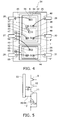
- FIG. 4 is a schematic plan arrangement view of a semiconductor package provided in a power supply device according to the second embodiment.
- the other portions of the power supply device according to the second embodiment can be the same as the portions in the first embodiment.
- connection by a bonding wire 55 is added to the semiconductor package 8 in the first embodiment.
- the source of the second switching element 11 is electrically connected to the land 33 of the lead frame via a bonding wire 50, the lead frame, and the bonding wire 55. As it is evident from FIG. 4 , the land 32 and the land 33 are separated.
- the source of the second switching element 11 is connected to the land 33 of the lead frame, it is possible to reduce the influence of the current collapse and the leak current on the second switching element 11 as well.
- a structure is also conceivable in which the first switching element 9, the current control element 10, and the second switching element 11 are arranged on a single land and the source of the second switching element 11 is connected to the land rather than the source of the current control element 10.
- the first switching element 9, the current control element 10, and the second switching element 11 are arranged on a single land and the source of the second switching element 11 is connected to the land rather than the source of the current control element 10.
- FIG. 5 is a schematic circuit diagram of the semiconductor package.
- the first switching element 9, the current control element 10, and the second switching element 11 are arranged on the land 32.
- the source of the second switching element 11 is connected to the land 32 via the bonding wires 50 and 55.
- Cds represents a capacity obtained by adding up a drain-to-source capacity and a drain-to-land capacity of the second switching element 11 connected in parallel.
- Cd represents the capacity of the diode 12.
- the capacity Cds Since the land 32 having a large area is connected to the source of the second switching element 11, the capacity Cds has a large value with respect to the capacity Cd.
- a voltage obtained by dividing an input voltage of the power supply device 3 by the capacity Cds and the capacity Cd is applied to the second switching element 11 and the diode 12. Since the capacity Cds is large with respect to the capacity Cd, a relatively large voltage is applied to the diode 12. It is likely that the voltage exceeds a withstand voltage between the gate and the source of the second switching element 11 and the second switching element 11 is broken.
- the land divided into three is examined.
- the first switching element 9, the current control element 10, and the second switching element 11 are respectively formed as single semiconductor chips.
- the semiconductor chips are respectively arranged on the lands and sources of the semiconductor chips are respectively connected to the lands. A problem also occurs in this structure.
- this structure Since a high voltage is applied, in the first switching element 9, this structure is effective as a measure against the current collapse and the leak current. On the other hand, as in the switching element 11 shown in FIG. 5 , a large capacity is connected between the drain and the source of the first switching element 9. Therefore, a switching operation of the first switching element 9 is delayed.
- the first switching element 9 and the current control element 10 are arranged on the land 32 and the second switching element 11 is arranged on the land 33 different from the land 32.
- a system for connecting the source of the current control element 10 to the land 32 and connecting the source of the second switching element 11 to the land 33 is considered to be a desirable form.
- an effect is obtained that it is possible to reduce the size of the power supply device 3 by packaging the first switching element 9, the current control element 10, and the second switching element 11 in one semiconductor package 8.
- An effect is also obtained that it is possible to suppress the influence of the current collapse and the leak current not only on the first switching element 9 and the current control element 10 but also on the second switching element 11 and suppress deterioration in conversion efficiency.
- the terminal 27 may be provided in a side portion of the semiconductor package 54 where the terminals 29 to 31 are provided.
- the terminal 27 By providing the terminal 27 in the side portion where the terminals 29 to 31 are provided, it is possible to divide a portion applied with a direct-current voltage or low-frequency pulsation and a portion applied with a high frequency.
- the semiconductor package 54 it is possible to secure a creepage distance of insulation and take measures against static electricity for the semiconductor package 54.
- FIG. 6 is a circuit diagram of a luminaire including a power supply device according to the third embodiment.
- FIG. 7 is a schematic plan arrangement view of a semiconductor package provided in the power supply device in the embodiment.
- a luminaire 56 includes the direct-current voltage source 2, a power supply device 57, and the lighting load 4.
- the power supply device 57 includes the input filter capacitor 7, a semiconductor package 58, the diodes 13 and 14, the constant voltage diode 15, the resistor 16, the capacitor 17, the inductors 18 and 19, and the output filter capacitor 20.
- the semiconductor package 58 in the embodiment includes the first switching element 9, the current control element 10, the second switching element 11, and the diode 12.
- the diode 12 is a GaN semiconductor same as the second switching element 11.
- a bonding pad 59 corresponds to an anode electrode and a bonding pad 60 corresponds to a cathode electrode.
- the anode of the diode 12 is connected to the terminal 31 via a bonding wire 61.
- the source of the switching element 11 is connected to the cathode of the diode 12 by a metal wire 62 formed between the pads.
- the diode 12 is included in the semiconductor package 8 in the power supply device 3 in the first embodiment to form the semiconductor package 58. Otherwise, the power supply device 57 is the same as the power supply device 3 in the first embodiment. The operation of the power supply device 57 is also the same as the operation of the power supply device 3.
- the terminal 27 may be provided in a side portion of the semiconductor package 58 where the terminals 29 to 31 are provided.
- the terminal 27 By providing the terminal 27 in the side portion where the terminals 29 to 31 are provided, it is possible to divide a portion applied with a direct-current voltage or low-frequency pulsation and a portion applied with a high frequency.
- the semiconductor package 58 it is possible to secure a creepage distance of insulation and take measures against static electricity for the semiconductor package 58.
- the first switching element 9, the current control element 10, and the second switching element 11 are not limited to the GaN-based HEMT.
- the first switching element 9, the current control element 10, and the second switching element 11 may be a semiconductor element formed by using a semiconductor having a wide band gap (a wide band gap semiconductor) such as silicon carbide (SiC), gallium nitride (GaN), or diamond as a semiconductor substrate.
- the wide band gap semiconductor means a semiconductor having a band gap wider than a band gap of gallium arsenide (GaAs) having the band gap of about 1.4 eV.
- the wide band gap semiconductor includes, for example, a semiconductor having a band gap equal to or wider than 1.5 eV, gallium phosphate (GaP having band gap of about 2.3 eV), gallium nitride (GaN having a band gap of about 3.4 eV), diamond (C having a band gap of about 5.27 eV), aluminum nitride (AlN having a band gap of about 5.9 eV), and silicon carbide (SiC).
- GaP gallium phosphate
- GaN gallium nitride
- diamond having a band gap of about 5.27 eV
- AlN aluminum nitride
- SiC silicon carbide
- the lighting load 4 is not limited to LED and may be, for example, an organic EL (Electro-Luminescence) or an OLED (Organic light-emitting diode).
- organic EL Electro-Luminescence
- OLED Organic light-emitting diode
Landscapes
- Engineering & Computer Science (AREA)
- Power Engineering (AREA)
- Dc-Dc Converters (AREA)
- Circuit Arrangement For Electric Light Sources In General (AREA)
- Junction Field-Effect Transistors (AREA)
Abstract
According to one embodiment, a power supply device (3, 57) includes a conductive first mounting board (32), a first switching element (9), a current control element (10), and a second switching element (11). The first switching element (9) is mounted on the first mounting board (32). The current control element (10) is mounted on the first mounting board (32), includes a main terminal connected to the first mounting board (32), is connected to the first switching element (9) in series, and is configured to limit an electric current of the first switching element (9). The second switching element (11) is connected to the current control element (10) in series. An electric current flows to the second switching element (11) when the first switching element (9) is off.
Description
- Embodiments described herein relate generally to a power supply device and a luminaire.
- In recent years, in a luminaire, as an illumination light source, an incandescent lamp and a fluorescent lamp are replaced with energy-saving and long-life light sources such as a light-emitting diode (LED). For example, new illumination light sources such as an EL (Electro-Luminescence) and an organic light-emitting diode are also developed.
- The brightness of the illumination light sources depends on a value of a flowing electric current. In order to stably light the luminaire, a power supply device of a constant current output type is necessary. It is necessary to convert a voltage in order to adjust an input power supply voltage to a rated voltage of an illumination light source such as an LED. As a highly efficient power supply suitable for power saving and a reduction in size, there are switching power supplies such as a DC-DC converter of a chopper system.
- As switching elements used in the switching power supplies, there are switching elements formed by a wide band gap compound semiconductor. Above all, a high electron mobility transistor (HEMT) formed by a nitride semiconductor such as gallium nitride (GaN) attracts attention. This is because the high electron mobility transistor has a high withstand voltage and a low ON resistance characteristic and can be switched at a high frequency. If ON resistance falls and high-speed switching can be performed, it is possible to reduce the sizes of an inductor and a capacitor configuring an output filter. In order to attain a reduction in the size of the entire power supply device, a reduction in the size of the element itself is also necessary. It is also necessary to simultaneously promote improvement of efficiency taking into account characteristics of the nitride semiconductor.
-
-
FIG. 1 is a circuit diagram illustrating a luminaire including a power supply device according to a first embodiment; -
FIG. 2 is a schematic plan arrangement view of a semiconductor package provided in the power supply device in the first embodiment; -
FIGS. 3A and 3B are characteristic diagrams showing a leak current characteristic of a GaN HEMT; -
FIG. 4 is a schematic plan arrangement view of a semiconductor package provided in a power supply device according to a second embodiment; -
FIG. 5 is a schematic circuit diagram of a semiconductor package; -
FIG. 6 is a circuit diagram illustrating a luminaire including a power supply device according to a third embodiment; and -
FIG. 7 is a schematic plan arrangement view of a semiconductor package provided in the power supply device in the third embodiment. - In general, according to one embodiment, a power supply device includes a conductive first mounting board, a first switching element, a current control element, and a second switching element. The first switching element is mounted on the first mounting board. The current control element is mounted on the first mounting board, includes a main terminal connected to the first mounting board, is connected to the first switching element in series, and is configured to limit an electric current of the first switching element. The second switching element is connected to the current control element in series. An electric current flows to the second switching element when the first switching element is off.
- According to another embodiment, there is provided a luminaire including a power supply device and a lighting load. The power supply device includes a first mounting board, a first switching element, a current control element, and a second switching element. The first mounting board is conductive. The first switching element is mounted on the first mounting board. The current control element is mounted on the first mounting board, includes a main terminal connected to the first mounting board, is connected to the first switching element in series, and limits an electric current of the first switching element. The second switching element is connected to the current control element in series. An electric current flows to the second switching element when the first switching element is off. The lighting load is a load circuit of the power supply device.
- Various embodiments will be described hereinafter with reference to the accompanying drawings. In the following explanation, the same members are denoted by the same reference numerals and signs. Explanation of the members once explained is omitted as appropriate.
-
FIG. 1 is a circuit diagram illustrating a luminaire including a power supply device according to a first embodiment. -
FIG. 2 is a schematic plan arrangement view of a semiconductor package provided in the power supply device in the embodiment. - A luminaire 1 includes a
power supply device 3 configured to covert an output voltage of a direct-current voltage source 2 into a desired voltage and alighting load 4 functioning as a load circuit of thepower supply device 3 and supplied with electric power from thepower supply device 3 to light. Thelighting load 4 includes an illumination light source such as an LED. The direct-current voltage source 2 includes, for example, an alternating-current power supply 5 and arectifier 6. InFIG. 1 , as the direct-current voltage source 2, a direct-current voltage source is shown that rectifies an alternating-current voltage of the alternating-current power supply 5 such as a commercial alternating-current power supply using therectifier 6 such as a bridge-type rectifier circuit and outputs a direct-current voltage. Thepower supply device 3 includes an input filter capacitor 7, asemiconductor package 8,diodes constant voltage diode 15, aresistor 16, acapacitor 17,inductors output filter capacitor 20. Thesemiconductor package 8 includes afirst switching element 9, acurrent control element 10, and asecond switching element 11. These elements are normally on type transistors formed by a compound semiconductor, for example, high electron mobility transistors (HEMTs) formed by a nitride semiconductor such as gallium nitride (GaN). Thediode 12 is, for example, a silicon Schottky barrier diode. Theinductor 18 and theinductor 19 are magnetically coupled. - In this specification, the "nitride semiconductor" includes semiconductors having all compositions obtained by changing composition ratios x, y, and z within ranges of the composition ratios in a chemical formula BxInyAlzGa 1-x-y-zN (0≤x≤1, 0≤y≤1, 0≤z≤1, x+y+z≤1). Further, semiconductors further including group V elements other than N (nitride), semiconductors further including various elements added to control various physical properties such as a conduction type, and semiconductors further including unintentionally-included various elements are also included in the "nitride semiconductor".
- An output of the direct-
current voltage source 2 is input to between a high-potential input terminal 21 and a low-potential input terminal 22 of thepower supply device 3. The input filter capacitor 7 is connected between the high-potential input terminal 21 and the low-potential input terminal 22 of thepower supply device 3. The high-potential input terminal 21 of thepower supply device 3 is connected to a drain of thefirst switching element 9. A source of thefirst switching element 9 is connected to a drain of the secondcurrent control element 10. A source of thecurrent control element 10 is connected to a drain of thesecond switching element 11. A source of thesecond switching element 11 is connected to a cathode of thediode 12. - An anode of the
diode 12 is connected to the low-potential input terminal 22 of thepower supply device 3. The drain of thesecond switching element 11 is connected to one end of thefirst inductor 18. The other end of thefirst inductor 18 is connected to one end of theoutput filter capacitor 20. The other end of theoutput filter capacitor 20 is connected to a low-potential input terminal of thepower supply device 3. One end of thesecond inductor 19 is connected to the drain of thesecond switching element 11. The other end of thesecond inductor 19 is connected to a gate of thefirst switching element 9 via thecapacitor 17. Thesecond inductor 19 is a line in which a voltage for turning on thefirst switching element 9 is induced when an electric current of thefirst inductor 18 increases and a voltage for turning off thefirst switching element 9 is induced when the electric current of thefirst inductor 18 decreases. - An anode of the
diode 14 is connected to the gate of thefirst switching element 9. A cathode of thediode 14 is connected to the source of thecurrent control element 10. An anode of thediode 13 is connected to a gate of thecurrent control element 10. A cathode of thediode 13 is connected to the source of thecurrent control element 10. A gate of thesecond switching element 11 is connected to the anode of thediode 12. A cathode of theconstant voltage diode 15 is connected to the drain of thesecond switching element 11. An anode of theconstant voltage diode 15 is connected to one end of theresistor 16. The other end of theresistor 16 is connected to the low-potential input terminal 22 of thepower supply device 3. The gate of thecurrent control element 10 is connected to the anode of theconstant voltage diode 15. An output of thepower supply device 3 is extracted to the high-potential output terminal 23 and the low-potential output terminal 24 from both ends of theoutput filter capacitor 20 and supplied to thelighting load 4. - As shown in
FIG. 2 , asemiconductor chip 34 and asemiconductor chip 35 are packaged in thesemiconductor package 8.FIG. 2 is a plan view schematically showing the internal structure of thesemiconductor package 8. Actually, thesemiconductor chip 34 and thesemiconductor chip 35 are molded by sealingresin 25. Thesemiconductor chip 34 is mounted on a land (a first mounting board) 32 of a lead frame. Thesemiconductor chip 35 is mounted on a land (a second mounting board) 33 of the lead frame. Thelands lands resin 25 and packaged. - The
semiconductor chip 34 includes thefirst switching element 9 and thecurrent control element 10. Thesemiconductor chip 35 includes thesecond switching element 11. Bonding pads are formed on the semiconductor chips 34 and 35.Bonding pads first switching element 9, thecurrent control element 10, and thesecond switching element 11.Bonding pads first switching element 9, thecurrent control element 10, and thesecond switching element 11. Further,bonding pads first switching element 9, thecurrent control element 10, and thesecond switching element 11. Except thebonding pads wires 45 to 51. - The lead frames are drawn out to the outside as
terminals 26 to 31. The drain of theswitching element 9 is connected to the terminal 26. The gate of theswitching element 9 is connected to the terminal 29. The source of thecurrent control element 10 is connected to the terminal 27. The gate of thecurrent control element 10 is connected to the terminal 30. The drain of the switchingelement 11 is connected to the terminal 27. The source of the switchingelement 11 is connected to the terminal 28. The gate of the switchingelement 11 is connected to the terminal 31. - The source of the
switching element 9 is connected to the drain of thecurrent control element 10 by ametal wire 53 formed between pads. - The source of the
current control element 10 is electrically connected to theland 32 of the lead frame via abonding wire 47, a lead frame, and abonding wire 52. - The operation of the
power supply device 3 is explained. - First, the operation of the
second switching element 11 and thediode 12 is explained. Thesecond switching element 11 and thediode 12 operate as rectifying means. When a positive voltage is applied to the anode side of thediode 12, thediode 12 conducts. Thesecond switching element 11, which is a normally on type element, is turned on. This state is a state in which a voltage is applied in a forward direction. The rectifying means changes to an ON state. When a negative voltage is applied to the anode side of thediode 12, thediode 12 becomes non-conductive. Since a gate-to-source voltage Vgs11 of thesecond switching element 11 has a negative value, thesecond switching element 11 is turned off. This is a state in which a voltage is applied in a backward direction. The rectifying means changes to an OFF state. - When a voltage is applied in the backward direction, a backward voltage applied to the
diode 12 is the gate-to-source voltage Vgs11 of thesecond switching element 11. Since this voltage is a voltage of about several voltage, a low-withstand voltage silicon Schottky barrier diode or the like can be used as thediode 12. In general, the low-withstand voltage silicon Schottky barrier diode has a low forward voltage. A forward voltage at the ON time of thesecond switching element 11 is also low. Therefore, a forward voltage of the rectifying means as a whole can be set lower than a forward voltage of a GaN diode alone. - The operation of the
current control element 10 is explained. - A gate-to-source voltage Vgs10 of the
current control element 10 is a negative voltage according to the action of theconstant voltage diode 15 and theresistor 16. Thecurrent control element 10 has a threshold current corresponding to the gate-to-source voltage Vgs10. When a drain current of thecurrent control element 10 is smaller than the threshold current, thecurrent control element 10 shows low ON resistance. When the drain current exceeds the threshold current, the ON resistance of thecurrent control element 10 suddenly increases. Thecurrent control element 10 shows a constant current characteristic. - The operation of the
power supply device 3 is explained below with reference to the characteristics of the rectifying means formed by thesecond switching element 11 and thediode 12 and thecurrent control element 10. - (1) When an output voltage of the direct-
current power supply 2 is applied between the high-potential input terminal 21 and the low-potential input terminal 22, thefirst switching element 9 and thecurrent control element 10 are in the ON state because the elements are the normally on type elements. Then, an electric current flows through a path of the high-potential input terminal 21, thefirst switching element 9, thecurrent control element 10, theinductor 18, theoutput filter capacitor 20, and the low-potential input terminal 22. Theoutput filter capacitor 20 is charged. Electromagnetic energy is accumulated in theinductor 18. - (2) Since the
first switching element 9 and thecurrent control element 10 are on, an input voltage of thepower supply device 3 is applied to both ends of the rectifying means formed by thesecond switching element 11 and thediode 12. Since a voltage is applied in the backward direction, the rectifying means changes to a non-conduction state. - (3) The electric current flowing through the
inductor 18 increases as time elapses. Since theinductor 19 is magnetically coupled with theinductor 18, an electromotive force for setting the side of thecapacitor 17 operating as a coupling capacitor to high potential is inducted in theinductor 19. Potential, which is positive with respect to the source, is supplied to the gate of thefirst switching element 9 via thecapacitor 17. Thefirst switching element 9 maintains the ON state. - (4) When the electric current flowing through the
inductor 18 exceeds the threshold current of thecurrent control element 10, a drain-to-source voltage of thecurrent control element 10 suddenly increases according to the sudden increase of the ON resistance. A gate-to-source voltage of thefirst switching element 9 has a negative large value. Thefirst switching element 9 is turned off. - (5) A counter electromotive force is generated in the
inductor 18. Since a voltage is applied in the forward direction, the rectifying means formed by thesecond switching element 11 and thediode 12 changes to the ON state. The electric current continues to flow through a path of the rectifying means, theinductor 18, and theoutput filter capacitor 20. Since the electromagnetic energy is emitted, the electric current of theinductor 18 decreases. A negative voltage induced in theinductor 19 is maintained. Thefirst switching element 9 maintains the OFF state. - (6) When the electromagnetic energy accumulated in the
inductor 18 decreases to zero, the electric current flowing through theinductor 18 decreases to zero. The direction of the electromotive force is reversed again. An electromotive force for setting thecapacitor 17 side to high potential is induced in theinductor 19. A voltage higher than the voltage at the source is supplied to the gate of thefirst switching element 9. Thefirst switching element 9 is turned on. Thepower supply device 3 returns to the state of (1). - Thereafter,
power supply device 3 repeats (1) to (6). The input voltage is converted and supplied to thelighting load 4. In the first embodiment, thepower supply device 3 operates as a falling voltage converter. Thediodes first switching element 9 and thecurrent control element 10. - In the HEMT formed by the GaN-based semiconductor, there is a phenomenon called current collapse in which a drain current is affected by a drain-to-source voltage. This is a phenomenon in which the ON resistance of the GaN HEMT rises immediately after a high-voltage is applied thereto. As a measure against this phenomenon, there is a method of electrically connecting a source terminal or a gate terminal of the GaN HEMT to a land of a lead frame.
- An effect of the measure is explained using Table 1.
- Table 1 is a table illustrating a change in the ON resistance before and after the voltage application to the GaN HEMT. That is, Table 1 represents, with the ON resistance before the voltage application set as a reference, a change in the ON resistance before and after application of a voltage of 500 V between the drain and the source of the GaN HEMT.
Table 1 Connection form of the lead frame land and the terminal Change in the ON resistance Source terminal is connected 1.08 times Gate terminal is connected 1.11 times No terminal is connected 1.63 times - It is seen that, when the source or the gate is connected to the land of the lead frame, an increase in the ON resistance is small compared with the increase in the ON resistance that occurs when the source and the gate are not connected to the land of the lead frame. As explained above, in the semiconductor package shown in
FIG. 2 , the source of thecurrent control element 10 is connected to theland 33 of the lead frame. Consequently, it is possible to reduce the influence of the current collapse concerning the switchingelement 9 and thecurrent control element 10. - Other effects are explained with reference to
FIGS. 3A and 3B . -
FIGS. 3A and 3B are characteristic diagrams showing a leak current characteristic of the GaN HEMT. - The abscissa of
FIG. 3B indicates a drain-to-gate voltage Vdg of the GaN HEMT obtained when a backward voltage is applied to the rectifying means formed by the GaN HEMT and the diode and changing the GaN HEMT to the OFF state. The first ordinate ofFIG. 3B indicates a source-to-gate voltage Vsg and the second ordinate ofFIG. 3B indicates a leak current IR. - It is seen that, when the gate is connected to the land of the lead frame, the leak current IR increases according to an increase in the drain-to-gate voltage Vdg. When the leak current IR increases, conversion efficiency of the
power supply device 3 is deteriorated. The increase in the leak current IR causes an increase in the source-to-gate voltage Vsg and causes further deterioration in the conversion efficiency. This is because, in order to apply a forward voltage to turn on the GaN HEMT, it is necessary to discharge the source-to-gate voltage Vsg and this discharged power is a loss. - On the other hand, when the source is connected to the land of the lead frame and when both the terminals are not connected, the leak current IR and the source-to-gate voltage Vsg hardly increase.
- It is seen from these results that it is possible to cope with both of the current collapse and the leak current by connecting the source of the GaN HEMT to the land of the lead frame.
- Effects of the first embodiment are explained. An effect is obtained that it is possible to reduce the size of the
power supply device 3 by packaging thefirst switching element 9, thecurrent control element 10, and thesecond switching element 11 in onesemiconductor package 8. It is possible to reduce the influence of the current collapse and suppress an increase in the ON resistance by connecting the source of thecurrent control element 10 to the land of the lead frame. At the same time, it is possible to suppress an increase in the leak current. Consequently, an effect is also obtained that deterioration in the conversion efficiency is suppressed. - In the embodiment, in the
semiconductor package 8, the terminal 27 is provided in a side portion where theterminals semiconductor package 8 where theterminals 29 to 31 are provided. By providing the terminal 27 in the side portion where theterminals 29 to 31 are provided, it is possible to divide a portion applied with a direct-current voltage or low-frequency pulsation and a portion applied with a high frequency. In thesemiconductor package 8, it is possible to secure a creepage distance of insulation and take measures against static electricity for thesemiconductor package 8. - A second embodiment is explained.
-
FIG. 4 is a schematic plan arrangement view of a semiconductor package provided in a power supply device according to the second embodiment. - The other portions of the power supply device according to the second embodiment can be the same as the portions in the first embodiment.
- In a
semiconductor package 54 of the power supply device in the embodiment, connection by abonding wire 55 is added to thesemiconductor package 8 in the first embodiment. The source of thesecond switching element 11 is electrically connected to theland 33 of the lead frame via abonding wire 50, the lead frame, and thebonding wire 55. As it is evident fromFIG. 4 , theland 32 and theland 33 are separated. - Since the source of the
second switching element 11 is connected to theland 33 of the lead frame, it is possible to reduce the influence of the current collapse and the leak current on thesecond switching element 11 as well. - A structure is also conceivable in which the
first switching element 9, thecurrent control element 10, and thesecond switching element 11 are arranged on a single land and the source of thesecond switching element 11 is connected to the land rather than the source of thecurrent control element 10. However, in this structure, a problem explained below occurs. - Since the source of the
second switching element 11 is connected to the single land, a large capacity is connected between the drain and the source of thesecond switching element 11. This state is shown inFIG. 5 . -
FIG. 5 is a schematic circuit diagram of the semiconductor package. - The
first switching element 9, thecurrent control element 10, and thesecond switching element 11 are arranged on theland 32. The source of thesecond switching element 11 is connected to theland 32 via thebonding wires second switching element 11 connected in parallel. Cd represents the capacity of thediode 12. - Since the
land 32 having a large area is connected to the source of thesecond switching element 11, the capacity Cds has a large value with respect to the capacity Cd. When thefirst switching element 9 and thecurrent control element 10 are in the ON state, a voltage obtained by dividing an input voltage of thepower supply device 3 by the capacity Cds and the capacity Cd is applied to thesecond switching element 11 and thediode 12. Since the capacity Cds is large with respect to the capacity Cd, a relatively large voltage is applied to thediode 12. It is likely that the voltage exceeds a withstand voltage between the gate and the source of thesecond switching element 11 and thesecond switching element 11 is broken. - The land divided into three is examined.
- The
first switching element 9, thecurrent control element 10, and thesecond switching element 11 are respectively formed as single semiconductor chips. The semiconductor chips are respectively arranged on the lands and sources of the semiconductor chips are respectively connected to the lands. A problem also occurs in this structure. - Since a high voltage is applied, in the
first switching element 9, this structure is effective as a measure against the current collapse and the leak current. On the other hand, as in the switchingelement 11 shown inFIG. 5 , a large capacity is connected between the drain and the source of thefirst switching element 9. Therefore, a switching operation of thefirst switching element 9 is delayed. - On the other hand, in the
current control element 10, since an applied voltage during the OFF state is low, the current collapse is not a serious problem. There is almost no necessity of connecting the source of thecurrent control element 10 to the land. - Based on the above examination, as explained in the embodiment shown in
FIG. 4 , thefirst switching element 9 and thecurrent control element 10 are arranged on theland 32 and thesecond switching element 11 is arranged on theland 33 different from theland 32. A system for connecting the source of thecurrent control element 10 to theland 32 and connecting the source of thesecond switching element 11 to theland 33 is considered to be a desirable form. - Effects of the second embodiment are explained.
- As in the first embodiment, an effect is obtained that it is possible to reduce the size of the
power supply device 3 by packaging thefirst switching element 9, thecurrent control element 10, and thesecond switching element 11 in onesemiconductor package 8. An effect is also obtained that it is possible to suppress the influence of the current collapse and the leak current not only on thefirst switching element 9 and thecurrent control element 10 but also on thesecond switching element 11 and suppress deterioration in conversion efficiency. - In the embodiment, as in the first embodiment, the terminal 27 may be provided in a side portion of the
semiconductor package 54 where theterminals 29 to 31 are provided. By providing the terminal 27 in the side portion where theterminals 29 to 31 are provided, it is possible to divide a portion applied with a direct-current voltage or low-frequency pulsation and a portion applied with a high frequency. In thesemiconductor package 54, it is possible to secure a creepage distance of insulation and take measures against static electricity for thesemiconductor package 54. - A third embodiment is explained.
-
FIG. 6 is a circuit diagram of a luminaire including a power supply device according to the third embodiment. -
FIG. 7 is a schematic plan arrangement view of a semiconductor package provided in the power supply device in the embodiment. - As shown in
FIG. 6 , aluminaire 56 includes the direct-current voltage source 2, apower supply device 57, and thelighting load 4. - The
power supply device 57 includes the input filter capacitor 7, asemiconductor package 58, thediodes constant voltage diode 15, theresistor 16, thecapacitor 17, theinductors output filter capacitor 20. - As shown in
FIG. 7 , thesemiconductor package 58 in the embodiment includes thefirst switching element 9, thecurrent control element 10, thesecond switching element 11, and thediode 12. Thediode 12 is a GaN semiconductor same as thesecond switching element 11. - A
bonding pad 59 corresponds to an anode electrode and abonding pad 60 corresponds to a cathode electrode. The anode of thediode 12 is connected to the terminal 31 via abonding wire 61. The source of the switchingelement 11 is connected to the cathode of thediode 12 by ametal wire 62 formed between the pads. - In the
power supply device 57 in the embodiment, thediode 12 is included in thesemiconductor package 8 in thepower supply device 3 in the first embodiment to form thesemiconductor package 58. Otherwise, thepower supply device 57 is the same as thepower supply device 3 in the first embodiment. The operation of thepower supply device 57 is also the same as the operation of thepower supply device 3. - Effects of the third embodiment are explained. According to the embodiment, as in the first embodiment, an effect is obtained that it is possible to suppress the influence of the current collapse and the leak current on the
first switching element 9 and thecurrent control element 10 and suppress deterioration in conversion efficiency. Since thefirst switching element 9, thecurrent control element 10, thesecond switching element 11, and thediode 12 are packaged in onesemiconductor package 58, an effect is also obtained that it is possible to further reduce the size of thepower supply device 57 than in the first embodiment. - In the embodiment, as in the first and second embodiments, the terminal 27 may be provided in a side portion of the
semiconductor package 58 where theterminals 29 to 31 are provided. By providing the terminal 27 in the side portion where theterminals 29 to 31 are provided, it is possible to divide a portion applied with a direct-current voltage or low-frequency pulsation and a portion applied with a high frequency. In thesemiconductor package 58, it is possible to secure a creepage distance of insulation and take measures against static electricity for thesemiconductor package 58. - The embodiments are explained above with reference to the specific examples. However, the embodiments are not limited to the specific examples and various modifications of the embodiments are possible.
- For example, the
first switching element 9, thecurrent control element 10, and thesecond switching element 11 are not limited to the GaN-based HEMT. For example, thefirst switching element 9, thecurrent control element 10, and thesecond switching element 11 may be a semiconductor element formed by using a semiconductor having a wide band gap (a wide band gap semiconductor) such as silicon carbide (SiC), gallium nitride (GaN), or diamond as a semiconductor substrate. The wide band gap semiconductor means a semiconductor having a band gap wider than a band gap of gallium arsenide (GaAs) having the band gap of about 1.4 eV. The wide band gap semiconductor includes, for example, a semiconductor having a band gap equal to or wider than 1.5 eV, gallium phosphate (GaP having band gap of about 2.3 eV), gallium nitride (GaN having a band gap of about 3.4 eV), diamond (C having a band gap of about 5.27 eV), aluminum nitride (AlN having a band gap of about 5.9 eV), and silicon carbide (SiC). - The
lighting load 4 is not limited to LED and may be, for example, an organic EL (Electro-Luminescence) or an OLED (Organic light-emitting diode). - The embodiments are explained above with reference to the specific examples. However, the embodiments are not limited to the specific examples. That is, examples obtained by those skilled in the art applying design changes to the specific examples are also included in the scope of the embodiments as long as the examples include the characteristics of the embodiments. The components and the arrangement, the materials, the conditions, the shapes, the sizes, and the like of the components included in the specific examples are not limited to those illustrated in the figures and can be changed as appropriate.
- The components included in the embodiments can be combined as long as the combination is technically possible. Components obtained by combining the components are also included in the scope of the embodiments as long as the components include the characteristics of the embodiments. Besides, in the category of the idea of the embodiments, those skilled in the art can conceive various modifications and alterations. It is understood that the modifications and the alternations also belong to the scope of the embodiments.
- While certain embodiments have been described, these embodiments have been presented by way of example only, and are not intended to limit the scope of the inventions. Indeed, the novel embodiments described herein may be embodied in a variety of other forms; furthermore, various omissions, substitutions and changes in the form of the embodiments described herein may be made without departing from the spirit of the inventions. The accompanying claims and their equivalents are intended to cover such forms or modifications as would fall within the scope and spirit of the inventions.
Claims (5)
- A power supply device (3, 57) comprising:a conductive first mounting board (32);a first switching element (9) mounted on the first mounting board (32);a current control element (10) mounted on the first mounting board (32), including a main terminal connected to the first mounting board (32), connected to the first switching element (9) in series, and configured to limit an electric current of the first switching element (9); anda second switching element (11) connected to the current control element (10) in series, an electric current flowing to the second switching element (11) when the first switching element (9) is off.
- The device (3, 57) according to claim 1, further comprising a second mounting board (33) on which the second switching element (11) is mounted,
a main terminal of the second switching element (11) being connected to the second mounting board (33), and
the first mounting board (32) and the second mounting board (33) being separated. - The device (3, 57) according to claim 2, wherein the first mounting board (32) and the second mounting board (33) are provided in a same semiconductor package (8, 54, 58).
- The device (3, 57) according to any one of claims 1 to 3, wherein the first switching element (9) and the current control element (10) are provided in a same semiconductor chip (34).
- A luminaire (1, 56) comprising:the power supply device (3, 57) according to any one of claims 1 to 4; anda lighting load (4) functioning as a load circuit of the power supply device (3, 57).
Applications Claiming Priority (1)
| Application Number | Priority Date | Filing Date | Title |
|---|---|---|---|
| JP2013198451A JP6156643B2 (en) | 2013-09-25 | 2013-09-25 | Power supply device and lighting device |
Publications (1)
| Publication Number | Publication Date |
|---|---|
| EP2863710A2 true EP2863710A2 (en) | 2015-04-22 |
Family
ID=50241235
Family Applications (1)
| Application Number | Title | Priority Date | Filing Date |
|---|---|---|---|
| EP20140159159 Withdrawn EP2863710A2 (en) | 2013-09-25 | 2014-03-12 | Power supply device and luminaire |
Country Status (4)
| Country | Link |
|---|---|
| US (1) | US20150084530A1 (en) |
| EP (1) | EP2863710A2 (en) |
| JP (1) | JP6156643B2 (en) |
| CN (1) | CN104470048B (en) |
Families Citing this family (8)
| Publication number | Priority date | Publication date | Assignee | Title |
|---|---|---|---|---|
| US8488342B2 (en) | 2008-10-21 | 2013-07-16 | On-Bright Electronics (Shanghai) Co., Ltd. | Systems and methods for constant voltage mode and constant current mode in flyback power converters with primary-side sensing and regulation |
| CN102769383B (en) | 2011-05-05 | 2015-02-04 | 广州昂宝电子有限公司 | System and method for constant-current control via primary side sensing and regulating |
| CN105246194B (en) | 2011-11-15 | 2018-07-03 | 昂宝电子(上海)有限公司 | For the LED illumination System and method of the current constant control in various operation modes |
| CN103368400B (en) | 2012-03-31 | 2015-02-18 | 昂宝电子(上海)有限公司 | System and method for constant voltage control and constant current control |
| CN102790531B (en) | 2012-07-24 | 2015-05-27 | 昂宝电子(上海)有限公司 | System for electric current control of power supply alternation system |
| CN103956900B (en) | 2014-04-23 | 2017-08-11 | 广州昂宝电子有限公司 | Systems and methods for output current regulation in power conversion systems |
| US9991776B2 (en) * | 2015-12-16 | 2018-06-05 | Semiconductor Components Industries, Llc | Switched mode power supply converter |
| JP7178184B2 (en) * | 2018-06-07 | 2022-11-25 | ローム株式会社 | semiconductor equipment |
Family Cites Families (5)
| Publication number | Priority date | Publication date | Assignee | Title |
|---|---|---|---|---|
| JP5358882B2 (en) * | 2007-02-09 | 2013-12-04 | サンケン電気株式会社 | Composite semiconductor device including rectifying element |
| JP5297104B2 (en) * | 2008-07-01 | 2013-09-25 | ルネサスエレクトロニクス株式会社 | Semiconductor device |
| JP5751483B2 (en) * | 2010-06-28 | 2015-07-22 | 東芝ライテック株式会社 | Switching power supply device, switching power supply circuit, and electrical equipment |
| JP2013013231A (en) * | 2011-06-29 | 2013-01-17 | Toshiba Lighting & Technology Corp | Switching power supply and illumination apparatus |
| JP5780428B2 (en) * | 2011-09-20 | 2015-09-16 | 東芝ライテック株式会社 | Switching power supply and lighting device |
-
2013
- 2013-09-25 JP JP2013198451A patent/JP6156643B2/en active Active
-
2014
- 2014-03-12 EP EP20140159159 patent/EP2863710A2/en not_active Withdrawn
- 2014-03-14 CN CN201410095297.4A patent/CN104470048B/en active Active
- 2014-03-14 US US14/211,214 patent/US20150084530A1/en not_active Abandoned
Non-Patent Citations (1)
| Title |
|---|
| None |
Also Published As
| Publication number | Publication date |
|---|---|
| US20150084530A1 (en) | 2015-03-26 |
| JP6156643B2 (en) | 2017-07-05 |
| CN104470048B (en) | 2018-09-18 |
| JP2015065044A (en) | 2015-04-09 |
| CN104470048A (en) | 2015-03-25 |
Similar Documents
| Publication | Publication Date | Title |
|---|---|---|
| EP2863710A2 (en) | Power supply device and luminaire | |
| CN103840821B (en) | Cascade semiconductor equipment | |
| US12588573B2 (en) | Semiconductor device | |
| CN102857104B (en) | Switching power supply and luminaire | |
| KR20150000815A (en) | Semiconductor device | |
| JP2016164983A (en) | Led drive and associated lighting system | |
| TWI663893B (en) | Led driver and illumination system related to the same | |
| JP6388181B2 (en) | Semiconductor package and power supply device | |
| CN105939549B (en) | Driver of light emitting diode and related lighting system | |
| JP5660351B2 (en) | Switching power supply and lighting device | |
| EP2854270A1 (en) | Rectifying circuit, electronic circuit, and electronic apparatus | |
| JP2015029040A (en) | Semiconductor module, LED driving device, and LED lighting device | |
| TWI678946B (en) | Led driver and illumination system related to the same | |
| TWI678944B (en) | Led driver and illumination system related to the same | |
| EP2863711A2 (en) | Power supply device and luminaire | |
| CN104065277A (en) | Power supply device and lighting device | |
| US20150084531A1 (en) | Power Supply Device and Luminaire | |
| JP2015065776A (en) | Power supply and illumination device | |
| Zibold et al. | High voltage GaN-based Schottky diodes in non-isolated LED buck converters | |
| TWI729540B (en) | Led driver and illumination system related to the same |
Legal Events
| Date | Code | Title | Description |
|---|---|---|---|
| PUAI | Public reference made under article 153(3) epc to a published international application that has entered the european phase |
Free format text: ORIGINAL CODE: 0009012 |
|
| 17P | Request for examination filed |
Effective date: 20140312 |
|
| AK | Designated contracting states |
Kind code of ref document: A2 Designated state(s): AL AT BE BG CH CY CZ DE DK EE ES FI FR GB GR HR HU IE IS IT LI LT LU LV MC MK MT NL NO PL PT RO RS SE SI SK SM TR |
|
| AX | Request for extension of the european patent |
Extension state: BA ME |
|
| STAA | Information on the status of an ep patent application or granted ep patent |
Free format text: STATUS: THE APPLICATION HAS BEEN WITHDRAWN |
|
| 18W | Application withdrawn |
Effective date: 20150427 |