EP2863653A1 - Integrated CMOS back cavity acoustic transducer and the method of producing the same - Google Patents
Integrated CMOS back cavity acoustic transducer and the method of producing the same Download PDFInfo
- Publication number
- EP2863653A1 EP2863653A1 EP20140250117 EP14250117A EP2863653A1 EP 2863653 A1 EP2863653 A1 EP 2863653A1 EP 20140250117 EP20140250117 EP 20140250117 EP 14250117 A EP14250117 A EP 14250117A EP 2863653 A1 EP2863653 A1 EP 2863653A1
- Authority
- EP
- European Patent Office
- Prior art keywords
- substrate
- mems device
- mems
- recited
- cmos
- Prior art date
- Legal status (The legal status is an assumption and is not a legal conclusion. Google has not performed a legal analysis and makes no representation as to the accuracy of the status listed.)
- Withdrawn
Links
Images






Classifications
-
- B—PERFORMING OPERATIONS; TRANSPORTING
- B81—MICROSTRUCTURAL TECHNOLOGY
- B81C—PROCESSES OR APPARATUS SPECIALLY ADAPTED FOR THE MANUFACTURE OR TREATMENT OF MICROSTRUCTURAL DEVICES OR SYSTEMS
- B81C1/00—Manufacture or treatment of devices or systems in or on a substrate
- B81C1/00015—Manufacture or treatment of devices or systems in or on a substrate for manufacturing microsystems
- B81C1/00222—Integrating an electronic processing unit with a micromechanical structure
- B81C1/00238—Joining a substrate with an electronic processing unit and a substrate with a micromechanical structure
-
- B—PERFORMING OPERATIONS; TRANSPORTING
- B81—MICROSTRUCTURAL TECHNOLOGY
- B81C—PROCESSES OR APPARATUS SPECIALLY ADAPTED FOR THE MANUFACTURE OR TREATMENT OF MICROSTRUCTURAL DEVICES OR SYSTEMS
- B81C1/00—Manufacture or treatment of devices or systems in or on a substrate
- B81C1/00015—Manufacture or treatment of devices or systems in or on a substrate for manufacturing microsystems
- B81C1/00261—Processes for packaging MEMS devices
- B81C1/00309—Processes for packaging MEMS devices suitable for fluid transfer from the MEMS out of the package or vice versa, e.g. transfer of liquid, gas, sound
-
- H—ELECTRICITY
- H04—ELECTRIC COMMUNICATION TECHNIQUE
- H04R—LOUDSPEAKERS, MICROPHONES, GRAMOPHONE PICK-UPS OR LIKE ACOUSTIC ELECTROMECHANICAL TRANSDUCERS; ELECTRIC HEARING AIDS; PUBLIC ADDRESS SYSTEMS
- H04R19/00—Electrostatic transducers
- H04R19/005—Electrostatic transducers using semiconductor materials
-
- H—ELECTRICITY
- H10—SEMICONDUCTOR DEVICES; ELECTRIC SOLID-STATE DEVICES NOT OTHERWISE PROVIDED FOR
- H10D—INORGANIC ELECTRIC SEMICONDUCTOR DEVICES
- H10D84/00—Integrated devices formed in or on semiconductor substrates that comprise only semiconducting layers, e.g. on Si wafers or on GaAs-on-Si wafers
- H10D84/80—Integrated devices formed in or on semiconductor substrates that comprise only semiconducting layers, e.g. on Si wafers or on GaAs-on-Si wafers characterised by the integration of at least one component covered by groups H10D12/00 or H10D30/00, e.g. integration of IGFETs
- H10D84/82—Integrated devices formed in or on semiconductor substrates that comprise only semiconducting layers, e.g. on Si wafers or on GaAs-on-Si wafers characterised by the integration of at least one component covered by groups H10D12/00 or H10D30/00, e.g. integration of IGFETs of only field-effect components
- H10D84/83—Integrated devices formed in or on semiconductor substrates that comprise only semiconducting layers, e.g. on Si wafers or on GaAs-on-Si wafers characterised by the integration of at least one component covered by groups H10D12/00 or H10D30/00, e.g. integration of IGFETs of only field-effect components of only insulated-gate FETs [IGFET]
- H10D84/85—Complementary IGFETs, e.g. CMOS
-
- H—ELECTRICITY
- H10—SEMICONDUCTOR DEVICES; ELECTRIC SOLID-STATE DEVICES NOT OTHERWISE PROVIDED FOR
- H10W—GENERIC PACKAGES, INTERCONNECTIONS, CONNECTORS OR OTHER CONSTRUCTIONAL DETAILS OF DEVICES COVERED BY CLASS H10
- H10W72/00—Interconnections or connectors in packages
- H10W72/90—Bond pads, in general
-
- B—PERFORMING OPERATIONS; TRANSPORTING
- B81—MICROSTRUCTURAL TECHNOLOGY
- B81B—MICROSTRUCTURAL DEVICES OR SYSTEMS, e.g. MICROMECHANICAL DEVICES
- B81B2201/00—Specific applications of microelectromechanical systems
- B81B2201/02—Sensors
- B81B2201/0257—Microphones or microspeakers
-
- B—PERFORMING OPERATIONS; TRANSPORTING
- B81—MICROSTRUCTURAL TECHNOLOGY
- B81B—MICROSTRUCTURAL DEVICES OR SYSTEMS, e.g. MICROMECHANICAL DEVICES
- B81B3/00—Devices comprising flexible or deformable elements, e.g. comprising elastic tongues or membranes
- B81B3/0018—Structures acting upon the moving or flexible element for transforming energy into mechanical movement or vice versa, i.e. actuators, sensors, generators
-
- B—PERFORMING OPERATIONS; TRANSPORTING
- B81—MICROSTRUCTURAL TECHNOLOGY
- B81C—PROCESSES OR APPARATUS SPECIALLY ADAPTED FOR THE MANUFACTURE OR TREATMENT OF MICROSTRUCTURAL DEVICES OR SYSTEMS
- B81C2203/00—Forming microstructural systems
- B81C2203/07—Integrating an electronic processing unit with a micromechanical structure
- B81C2203/0785—Transfer and j oin technology, i.e. forming the electronic processing unit and the micromechanical structure on separate substrates and joining the substrates
- B81C2203/0792—Forming interconnections between the electronic processing unit and the micromechanical structure
Definitions
- Various embodiments of the invention relate generally to a MEMS device and particularly to a method for manufacturing the same.
- MEMS devices in the form of acoustic transducers such as microphones and Micromachined Ultrasonic Transducers (MUTs) integrated with CMOS, are typically packaged in external cavity packages, which are much larger than the die and therefore occupy a large footprint on a circuit board. It is desirable to create a chip scale packaged (CSP) acoustic sensors with an integrated back cavity (IBC), however conventional CSP metho20.1ds such a Through Silicon Via (TSV) are generally not compatible with acoustic sensor fabrication processes. Accordingly, a conventional CSP cannot be employed and the footprint of the packaging is undesirably large.
- CSP chip scale packaged
- IBC integrated back cavity
- TSV Through Silicon Via
- a MEMS device includes a MEMS substrate with a movable element. Further included is a CMOS substrate with a cavity, the MEMS substrate is disposed on top of the CMOS substrate. Additionally, a back cavity is connected to the CMOS substrate, the back cavity being formed at least partially by the cavity in the CMOS substrate and the movable element being acoustically coupled to the back cavity.
- Micro-Electro-Mechanical Systems refers to a class of structures or devices fabricated using semiconductorlike processes and exhibiting mechanical characteristics such as the ability to move or deform. MEMS often, but not always, interact with electrical signals. MEMS devices include but are not limited to gyroscopes, accelerometers, magnetometers, pressure sensors, microphones, and radio-frequency components. Silicon wafers containing MEMS structures are referred to as MEMS wafers.
- MEMS device may refer to a semiconductor device implemented as a micro-electro-mechanical system.
- MEMS structure may refer to any feature that may be part of a larger MEMS device.
- An engineered silicon-on-insulator (ESOI) wafer may refer to a SOI wafer with cavities beneath the silicon device layer or substrate.
- Handle wafer typically refers to a thicker substrate used as a carrier for the thinner silicon device substrate in a silicon-on-insulator wafer. Handle substrate and handle wafer can be interchanged.
- a cavity may refer to an opening or recession in a substrate wafer and enclosure may refer to a fully enclosed space.
- Post may be a vertical structure in the cavity of the MEMS device for mechanical support.
- Standoff may be a vertical structure providing electrical contact.
- back cavity may refer to a partial enclosed cavity equalized to ambient pressure via Pressure Equalization Channels (PEC).
- PEC Pressure Equalization Channels
- back cavity is also referred to as back chamber.
- a back cavity formed within the CMOS-MEMS device can be referred to as integrated back cavity.
- Pressure equalization channel also referred to as leakage channels/paths, are acoustic channels for low frequency or static pressure equalization of back cavity to ambient pressure.
- a rigid structure within a MEMS device that moves when subject to force may be referred to as a plate.
- a back plate may be a perforated plate used as an electrode.
- perforations refer to acoustic openings for reducing air damping in moving plates.
- Acoustic port (or "port") may be an opening for sensing the acoustic pressure.
- Acoustic barrier may be a structure that prevents or delays acoustic pressure from reaching certain portions of the device.
- Linkage is a structure that provides compliant attachment to substrate through anchor.
- In plane bump stops are extensions of the plate which come in contact with the device seal to limit range of movement in the plane of the plate.
- Rotational bump stop are extensions of the plate to limit range of rotations.
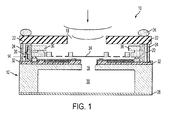
- a MEMS device 10 is shown, in accordance with an embodiment of the invention.
- the MEMS device 10 is shown to include a CMOS substrate 12 bonded to a MEMS substrate 14.
- the MEMS device 10 is a microphone and in another embodiment of the invention, the MEMS device 10 is an acoustic transducer such as MUTs.
- the MEMS device 10 may be a membrane type of microphone, a piston type of microphone, or a torsional type of microphone.
- the CMOS substrate 12 is bonded to the MEMS substrate 14 using Eutectic bonding although other suitable bonding methods are contemplated.
- the CMOS substrate is shown to be covered by a cap layer 28 at a surface opposite to a surface that is bonded with the CMOS substrate 12. Further included in the MEMS device 10, is a CMOS back cavity 30 that is connected to the MEMS substrate 14 through a cavity(or "port") 16.
- the cap layer 28 covers the back cavity 30.
- the cap layer 28 is made of conductive material, such as metal and is referred to herein as a "metal cover". In other embodiments, the cap layer 28 is made of non-conductive material that may include conductive material.
- the MEMS substrate 14 includes a movable element 34 that moves in response to acoustic waves received from the acoustic port 18 in the substrate 22.
- the back cavity 30 is connected to the CMOS substrate 12 and formed at least partially by a cavity in the CMOS substrate 12.
- the movable element 34 is acoustically coupled to the back cavity 30.
- Stud bumps 20 are shown disposed between the CMOS substrate 12 and a carrier substrate 22. More specifically, they are disposed on the metal pads 32 of the CMOS substrate 12 accordingly electrically connecting the CMOS substrate 12 to the carrier substrate 22.
- Fig. 1 Further shown in Fig. 1 is an optional underfill 24 disposed between the CMOS substrate 12 and the carrier substrate 22. Solder balls (or “solder metal") 26 are shown optionally formed on top of the carrier substrate 22.
- the carrier substrate 22 is made of laminate or ceramic.
- the stud bumps 20 are formed inside the underfill 24.
- the stud bumps 20 are made of gold.
- the stud bumps are made of any conductive material such as lead and tin.
- the stud bumps 20 are multiple stud bumps disposed on top of each other.
- the stud bumps are formed using a ball bonder.
- the MEMS movable element 34 is effectively formed on top of the CMOS substrate 12.
- the back cavity 30 is etched in the CMOS substrate 12 to enlarge the back cavity volume.
- the thickness of the remaining portion of the CMOS substrate 12 is marked, in Fig. 1 , by “h” and in an embodiment of the invention is approximately 20-100 micro meters (um).
- the width of the side wall of the back cavity 30, marked by "w", in Fig. 1 is approximately 20-200 um, in an exemplary embodiment of the invention.
- the volume of back cavity 30 is maximized while still maintaining a reasonable structural integrity for the device. Accordingly, performance of the MEMS device 10, particularly in embodiments such as a microphone, is improved while its footprint remains small.
- the cap layer 28 is connected to the CMOS substrate 12 by an epoxy (conductive or non-conductive), metal paste, or solder.
- the CSP package is realized by connecting the bond pads 32 on the CMOS substrate 12 to the substrate 22 by the stud bumps 20.
- the edge of the die is sealed with the underfill 24.
- the underfill 24 is made of epoxy or silicone.
- the substrate 22 is electrically connected to the stud bumps 20 by thermal or thermo-sonic compression bonding or another conductive bonding method.
- the port 16 and back cavity 30 are formed by separate etching steps.
- the port 16 is partially etched in a first etching step, with the second etching step forming the back cavity 30 and completing the etch of port 16.
- the back cavity 30 is approximately 100 um to 2 millimeters (mm).
- the back cavity 30 may be of any shape, including square-shaped or round-shaped.
- a handle wafer 36 which is optionally employed. The handle wafer 36 is shown disposed below the substrate 22.
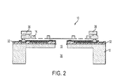
- Fig. 2 shows the MEMS device 10 before it is packaged.
- the handle wafer 36 is optional.
- the handle wafer 36 can act as a spacer when mounting to a carrier substrate and may also be used as an over-travel stop for the movable element 34
- the handle wafer 36 is made of silicon and is approximately 10um to 200um thick.
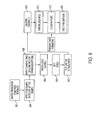
- Fig. 3 shows a process flow 300 for fabricating the MEMS device 10, in accordance with a method of the invention.
- the MEMS substrate 14 is bonded to the CMOS substrate 12 with the additional port 16 etched in the CMOS substrate 12.
- the steps 306 or 318 are performed. In the case where the handle wafer 36 is used, the process continues to step 306 and where no handle wafer is used, the process continues to the step 318.
- the chip is flipped and the cap layer 28 is disposed to cover the CMOS substrate 12 and the back cavity 30.
- wafer saw is performed and the chip is flipped back.
- laser dicing is used rather than wet wafer sawing to singulate wafer into die.
- step 310 stud bumps 20 are bonded to the CMOS substrate 12. It is noted that the steps 310 and 308 can be reversed with the step 310 being performed before the step 308.
- step 312 the die are bonded to a carrier substrate via the stud bumps 20 using a thermal or thermo-sonic compression bond.
- step 314 where underfill is disposed to seal the edges of the MEMS substrate 14. It is noted that steps 312 and 314 may be reversed if the underfill is cured to a "B-stage" prior to the compression bond.
- step 318 dry laser dicing rather than wet sawing is performed to singulate the MEMS wafer into die.
- step 320 the stud bumps 20 are bonded to the CMOS substrate 12. It is noted that the steps 318 and 320 may be done in any order.
- step 322 thermal or thermo-sonic compression bonding is performed via the stud bumps 20 between the carrier substrate 22 and singulated die.
- underfill 24 is used to seal the MEMS substrate 14. It is noted that steps 322 and 324 may be reversed if the underfill is cured to a "B-stage" prior to the compression bond.
- step 326 the chip is flipped and the CMOS substrate 12 and back cavity 30 are covered with the cap layer 28.
- step 326 follows the step 322 instead of the step 324.
- step 328 the chip is flipped and the solder balls 26 are formed on the carrier substrate 22.
- Figs. 4(a) to 4(f) show the process (Method A) of fabricating the MEMS device 10, in accordance with the steps 306 to 316 of Fig. 3 where a handle wafer is employed.
- the wafer is flipped and mounted on a tape 402.
- an adhesive is dispensed on top of the CMOS substrate 12, the cap layer 28 is mounted on top of the CMOS substrate 12 and the cavity 30, and the adhesive is cured on the wafer level.
- the cap layer 28 can be wafer-size or individually placed caps, as shown in Fig. 4(b) .
- the shape of the cap layer 28 can be plate-shaped or u-shaped (indented) to further increase the back volume of the MEMS device 10. In an exemplary embodiment, the total volume of the back cavity 30 is approximately 0.3 to 4 mm 3 .
- the electrical connection and bonding of the cap layer 28 to the CMOS substrate 12 can be formed by conductive epoxy compound or metal paste.
- Fig. 4(c) the wafer is diced as shown at 404 where the wafer is cut.
- the step of Fig. 4(c) is performed prior to the step of Fig. 4(b) .
- wafer dicing can be cutting or laser dicing.
- Fig. 4(d) the wafer is flipped and transferred to another tape and the stud bonds 20 are placed on top of the metal pads 32.
- the stud bonds 20 protrude above the top surface of the wafer handle 36.
- wafer dicing of step 4(c) can be done after the step of Fig. 4(d) .
- underfill 24 is optionally dispensed or screen printed on the stud bumps 20 to seal the MEMS substrate 14.
- the underfill 24 is alternatively dispensed or screen printed on the carrier substrate 22 and the edge of the die to seal the edge of the die, as shown in Fig. 4(e) .
- Step 4(e) is optional.
- step of 4(c) is not performed until after the step of Fig. 4(e) .
- the carrier substrate 22 with the port 18 is bonded tothe stud bumps 20 using thermal or thermo-sonic compression bonding to connect signals.
- Thermal compression is performed with or without dispensing underfill, as the case may be.
- Further details of the various ways of fabricating the MEMS device 10 is also disclosed in U.S. Patent Application No. 13/950,178, filed by Kim, Brian et al, on 7/24/2013 , and entitled "Assembly and Package of MEMS Device", the disclosure of which is incorporated by reference.
- Solder balls 26 are deposited onto or bonded to the carrier substrate 22.
- the stud bumps 20 electrically connect the carrier substrate 22 to the CMOS substrate 12.
- the stud bumps 20 maybe comprise one or more stud bumps stacked on top of each other.
- the carrier substrate 22 can be ceramic or a silicon interposer, and not epoxy-based.
- Figs. 5(a) to 5(e) show the process (Method B) of fabricating the MEMS device 10, in accordance with the steps 318 to 328 of Fig. 3 where a handle wafer is not employed.
- laser dicing is employed to separate the dies and the stud bumps 20 are attached to the device.
- the stud bumps 20 are attached prior to laser dicing.
- the dies are optionally transferred to another tape after singulation to form the stud bumps on the metal pads.
- the stud bumps protrude at least a few microns above the top surface of the MEMS substrate.
- underfill 24 is dispensed or screen printed on the stud bumps 20 and the edge of the die to seal the package edge.
- the carrier substrate 22 is bonded to the stud bumps 20 by thermal or thermo-sonic compression bonding.
- thermal or thermo-sonic compression in Fig. 5(c) is performed prior to the step shown in Fig. 5(b) .
- the carrier substrate 22 may optionally have solder balls deposited onto its outside surface (the surface opposite that one which the stud bumps are formed).
- die are picked up, flipped, and then mounted to a tape for CMOS back cavity capping. As shown in Fig.
- the cap layer 28 is attached to the CMOS substrate using the same method as described relative to Fig. 4(b) of Method A. If the carrier substrate 22 requires additional solder balls, the dies are flipped and attached to another tape to deposit the solder balls onto the carrier substrate, as shown in Fig. 5(e) .
- Method B uses the CMOS substrate etches as additional volume of the back cavity 30, which desirably improves the performance of the microphone and reduces the total package height in embodiments utilizing the MEMS device 10 as a microphone. Additionally, this method solves the process capability issues of the TSV-based integrated back cavity and requires minimal change to the integrated MEMS and CMOS microphone process.
- Figs. 6(a) - (c) show a two-step cavity etch process, in accordance with a method of the invention.
- the MEMS device 10 is shown to include a protection or sacrificial layer 604 disposed in the MEMS substrate 14 and a hard mask 602 disposed in the CMOS substrate 12.
- the sacrificial layer 604 is made of silicon oxide.
- the hard mask 602 which is at the back of the CMOS substrate 12, is formed to define the back cavity (30) pattern.
- a photoresist mask 606 with a smaller opening 608 is shown formed in Fig.
- the opening (or "cavity") 608 is shown partially etched using the photoresist mask 606, disposed on a bottom surface of the CMOS substrate 12.
- the photoresist mask 606 is removed and blanket etching is performed to form the larger cavity 610 and complete etching the opening 608.
- the blanket etching of Fig. 6(c) is stopped when opening 608 exposes the sacrificial layer 604.
- the partial etch depth of opening 608 in Fig. 6(b) in combination with the duration of the blanket etch of Fig. 6(c) determine the height "h" shown in Fig. 1 . Accordingly, the back cavity 30 and the port 16 connecting the CMOS substrate 12 to the MEMS substrate 14 are formed.
- the layer 604 is removed by etching to release the MEMS device 10.
- Fig. 7 shows a MEMS device 700, in accordance with another embodiment of the invention.
- the indented cap layer 700 extends the height of back cavity 30 providing additional back cavity volume.
- the MEMS device 10 can also have an inner seal ring, in accordance with yet another embodiment of the invention.
- the inner seal ring is acts as an acoustic seal when mounting the MEMS substrate 14 to a carrier substrate.
- the edges of the package device 10 may include a metal coating on the outer surface the package to form a Faraday cage for radio frequency (RF) shielding. The method of forming such a device is shown in Fig. 8 and 9(a) - (i) to follow.
- Fig. 8 is a flow chart of the steps performed in fabricating a MEMS device, in accordance with another method of the invention.
- step 802 during wafer fabrication, bond pads are exposed.
- step 804 stud bumps or solder-jetted bumps are formed.
- step 806 inner seal ring (or "landing ring") is applied for inner acoustic seal of the MEMS device and also to be used to absorb strain during packaging.
- the inner seal ring encircles the MEMS movable element and protrudes above the top surface of the stud bumps, in accordance with an embodiment of the invention.
- the inner seal ring in an exemplary embodiment, is made of a polymer or silicone material with suitable elasticity and characteristic of suitable adhesion to the substrate.
- the wafer is flipped and the capping layer 28 is applied to cap the back cavity 30 at the wafer level.
- the wafer is diced, at step 810, to form singulated dies.
- the chip is flipped again and a carrier substrate is bonded by thermal or thermo-sonic compression bonding via the stud-bumps at the same time, or through subsequent curing, also creating a physical or adhesive bond via the inner seal ring.
- the electrical connection between the chip and the carrier substrate is provided via the stud bumps.
- a silicone or molding material is filled in between dies.
- a wide curve saw dicing step is performed, at step 816, to cut through the molding material and partially into the substrate, followed by step 818, when a metal, such as nickel (Ni) or another type of metal layer coating is applied to form an RF shielding cage encapsulating the MEMS device.
- the metal coating is connected to ground or another defined potential via an electrical contact to the carrier substrate.
- a narrow curve saw dicing step is performed to cut through the metal and substrate to form a final packaged device Steps 816 through 820 are required for Faraday cage formation.
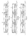
- Figs. 9(a) - 9(j) show the manufacturing process, in accordance with the flow chart of Fig. 8 , in fabricating a MEMS device with RF shielding and inner seal, in accordance with a method and embodiment of the invention.
- the MEMS device 900 is shown to include stud bumps 904 bonded to the substrate 910, which is held in place using the tape 902.
- the MEM substrate 908 is shown to be disposed on the CMOS substrate 910.
- an inner seal ring 912 is formed on top of the handle wafer 906.
- the inner seal (or landing ring) is made of silicone.
- a conductive material 926 e.g. the nickel is deposited via electro or electro less plating or an alternate metallization method. This is followed by singulation at step 9(i).
- Fig. 9(j) shows the final form of the MEMS device 900, after the steps 9(a) through 9(i), in accordance with an embodiment of the invention.
- Fig. 10 shows a MEMS device 1000, in accordance with another embodiment of the invention.
- the MEMS device 1000 is shown to have a MEMS acoustic element 1002 disposed on top of the CMOS substrate 1010 and more particularly, connected to a top metal layer 1006.
- the top metal layer 1006 is shown positioned on top of a lower metal layer 1004 and separated therefrom by dielectric 1012.
- each of the top metal layer 1006 and the lower metal layer 1004 is made of multiple metal layers.
- the dielectric 1012 is made of one or more dielectric layers.
- a port 1014 is shown through the CMOS substrate 1010 and under the MEMS acoustic element.
- a recess 1016 is shown formed under the MEMS acoustic element 1002 and surrounding the port 1014, formed by removal of one or more top metal and dielectric layers, such as the metal layer 1006.
- the CMOS circuits semiconductor circuits
- This approach maximizes the CMOS substrate area available for circuits, by minimizing the size of port 1014, while reducing damping under the acoustic element using recess 1016.
Landscapes
- Engineering & Computer Science (AREA)
- Manufacturing & Machinery (AREA)
- Microelectronics & Electronic Packaging (AREA)
- Physics & Mathematics (AREA)
- Acoustics & Sound (AREA)
- Signal Processing (AREA)
- Micromachines (AREA)
- Computer Hardware Design (AREA)
- Health & Medical Sciences (AREA)
- General Health & Medical Sciences (AREA)
- Toxicology (AREA)
Abstract
Description
- Various embodiments of the invention relate generally to a MEMS device and particularly to a method for manufacturing the same.
- MEMS devices in the form of acoustic transducers such as microphones and Micromachined Ultrasonic Transducers (MUTs) integrated with CMOS, are typically packaged in external cavity packages, which are much larger than the die and therefore occupy a large footprint on a circuit board. It is desirable to create a chip scale packaged (CSP) acoustic sensors with an integrated back cavity (IBC), however conventional CSP metho20.1ds such a Through Silicon Via (TSV) are generally not compatible with acoustic sensor fabrication processes. Accordingly, a conventional CSP cannot be employed and the footprint of the packaging is undesirably large.
- What is desired is a small-footprint acoustic device without comprising performance.
- Briefly, a MEMS device includes a MEMS substrate with a movable element. Further included is a CMOS substrate with a cavity, the MEMS substrate is disposed on top of the CMOS substrate. Additionally, a back cavity is connected to the CMOS substrate, the back cavity being formed at least partially by the cavity in the CMOS substrate and the movable element being acoustically coupled to the back cavity.
- A further understanding of the nature and the advantages of particular embodiments disclosed herein may be realized by reference of the remaining portions of the specification and the attached drawings.
-
-
Fig. 1 shows a MEMS device, in accordance with an embodiment of the invention. -
Fig. 2 shows theMEMS device 10 before it is packaged -
Fig. 3 shows aprocess flow 300 for fabricating theMEMS device 10, in accordance with a method of the invention. -
Figs. 4(a) to 4(f) show the process (Method A) of fabricating theMEMS device 10, in accordance with thesteps 306 to 316 ofFig. 3 where a handle wafer is employed. -
Figs. 5(a) to 5(e) show the process (Method B) of fabricating theMEMS device 10, in accordance with thesteps 318 to 328 ofFig. 3 where a handle wafer is not employed. -
Figs. 6(a) - (c) show a two-step cavity etch process, in accordance with a method of the invention. -
Fig. 7 shows aMEMS device 700, in accordance with another embodiment of the invention. -
Fig. 8 is a flow chart of the steps performed in fabricating a MEMS device, in accordance with another method of the invention. -
Figs. 9(a) - 9(j) show the manufacturing process, in accordance with the flow chart ofFig. 8 , in fabricating a MEMS device with RF shielding and inner seal, in accordance with a method and embodiment of the invention. -
Fig. 10 shows aMEMS device 1000, in accordance with another embodiment of the invention. - In the described embodiments Micro-Electro-Mechanical Systems (MEMS) refers to a class of structures or devices fabricated using semiconductorlike processes and exhibiting mechanical characteristics such as the ability to move or deform. MEMS often, but not always, interact with electrical signals. MEMS devices include but are not limited to gyroscopes, accelerometers, magnetometers, pressure sensors, microphones, and radio-frequency components. Silicon wafers containing MEMS structures are referred to as MEMS wafers.
- In the described embodiments, MEMS device may refer to a semiconductor device implemented as a micro-electro-mechanical system. MEMS structure may refer to any feature that may be part of a larger MEMS device. An engineered silicon-on-insulator (ESOI) wafer may refer to a SOI wafer with cavities beneath the silicon device layer or substrate. Handle wafer typically refers to a thicker substrate used as a carrier for the thinner silicon device substrate in a silicon-on-insulator wafer. Handle substrate and handle wafer can be interchanged.
- In the described embodiments, a cavity may refer to an opening or recession in a substrate wafer and enclosure may refer to a fully enclosed space. Post may be a vertical structure in the cavity of the MEMS device for mechanical support. Standoff may be a vertical structure providing electrical contact.
- In the described embodiments, back cavity may refer to a partial enclosed cavity equalized to ambient pressure via Pressure Equalization Channels (PEC). In some embodiments, back cavity is also referred to as back chamber. A back cavity formed within the CMOS-MEMS device can be referred to as integrated back cavity. Pressure equalization channel, also referred to as leakage channels/paths, are acoustic channels for low frequency or static pressure equalization of back cavity to ambient pressure.
- In the described embodiments, a rigid structure within a MEMS device that moves when subject to force may be referred to as a plate. A back plate may be a perforated plate used as an electrode.
- In the described embodiments, perforations refer to acoustic openings for reducing air damping in moving plates. Acoustic port (or "port") may be an opening for sensing the acoustic pressure. Acoustic barrier may be a structure that prevents or delays acoustic pressure from reaching certain portions of the device. Linkage is a structure that provides compliant attachment to substrate through anchor. In plane bump stops are extensions of the plate which come in contact with the device seal to limit range of movement in the plane of the plate. Rotational bump stop are extensions of the plate to limit range of rotations.
- Referring now to
Fig. 1 , aMEMS device 10 is shown, in accordance with an embodiment of the invention. TheMEMS device 10 is shown to include aCMOS substrate 12 bonded to aMEMS substrate 14. In an embodiment of the invention, theMEMS device 10 is a microphone and in another embodiment of the invention, theMEMS device 10 is an acoustic transducer such as MUTs. In the case of a microphone, theMEMS device 10 may be a membrane type of microphone, a piston type of microphone, or a torsional type of microphone. Further, in accordance with a method of the invention, theCMOS substrate 12 is bonded to theMEMS substrate 14 using Eutectic bonding although other suitable bonding methods are contemplated. - The CMOS substrate is shown to be covered by a
cap layer 28 at a surface opposite to a surface that is bonded with theCMOS substrate 12. Further included in theMEMS device 10, is aCMOS back cavity 30 that is connected to theMEMS substrate 14 through a cavity(or "port") 16. Thecap layer 28 covers theback cavity 30. In an embodiment of the invention, thecap layer 28 is made of conductive material, such as metal and is referred to herein as a "metal cover". In other embodiments, thecap layer 28 is made of non-conductive material that may include conductive material. TheMEMS substrate 14 includes amovable element 34 that moves in response to acoustic waves received from theacoustic port 18 in thesubstrate 22. - The
back cavity 30 is connected to theCMOS substrate 12 and formed at least partially by a cavity in theCMOS substrate 12. Themovable element 34 is acoustically coupled to theback cavity 30. -
Stud bumps 20 are shown disposed between theCMOS substrate 12 and acarrier substrate 22. More specifically, they are disposed on themetal pads 32 of theCMOS substrate 12 accordingly electrically connecting theCMOS substrate 12 to thecarrier substrate 22. - Further shown in
Fig. 1 is anoptional underfill 24 disposed between theCMOS substrate 12 and thecarrier substrate 22. Solder balls (or "solder metal") 26 are shown optionally formed on top of thecarrier substrate 22. - In some embodiments, the
carrier substrate 22 is made of laminate or ceramic. In an embodiment of the invention, the stud bumps 20 are formed inside theunderfill 24. In some embodiments of the invention, the stud bumps 20 are made of gold. In other embodiments, the stud bumps are made of any conductive material such as lead and tin. In still other embodiments of the invention, the stud bumps 20 are multiple stud bumps disposed on top of each other. In some embodiments of the invention, the stud bumps are formed using a ball bonder. - The MEMS
movable element 34 is effectively formed on top of theCMOS substrate 12. Theback cavity 30 is etched in theCMOS substrate 12 to enlarge the back cavity volume. The thickness of the remaining portion of theCMOS substrate 12 is marked, inFig. 1 , by "h" and in an embodiment of the invention is approximately 20-100 micro meters (um). The width of the side wall of theback cavity 30, marked by "w", inFig. 1 , is approximately 20-200 um, in an exemplary embodiment of the invention. In an exemplary embodiment, the volume ofback cavity 30 is maximized while still maintaining a reasonable structural integrity for the device. Accordingly, performance of theMEMS device 10, particularly in embodiments such as a microphone, is improved while its footprint remains small. - The
cap layer 28 is connected to theCMOS substrate 12 by an epoxy (conductive or non-conductive), metal paste, or solder. The CSP package is realized by connecting thebond pads 32 on theCMOS substrate 12 to thesubstrate 22 by the stud bumps 20. The edge of the die is sealed with theunderfill 24. In an exemplary embodiment, theunderfill 24 is made of epoxy or silicone. Thesubstrate 22 is electrically connected to the stud bumps 20 by thermal or thermo-sonic compression bonding or another conductive bonding method. - Applications of the various embodiments and methods shown and described herein include but are not limited to microphones, pressure sensors, resonators, switches, and other applicable devices.
- As will become further evident in the discussion and figures to follow, a two-step etching process is employed to create the
back cavity 30. In one embodiment, theport 16 andback cavity 30 are formed by separate etching steps. In another embodiment, theport 16 is partially etched in a first etching step, with the second etching step forming theback cavity 30 and completing the etch ofport 16. In an exemplary embodiment, theback cavity 30 is approximately 100 um to 2 millimeters (mm). Further, theback cavity 30 may be of any shape, including square-shaped or round-shaped. Further shown inFig. 1 , is ahandle wafer 36 which is optionally employed. Thehandle wafer 36 is shown disposed below thesubstrate 22. -
Fig. 2 shows theMEMS device 10 before it is packaged. As previously noted, thehandle wafer 36 is optional. Thehandle wafer 36 can act as a spacer when mounting to a carrier substrate and may also be used as an over-travel stop for themovable element 34 In an exemplary embodiment, thehandle wafer 36 is made of silicon and is approximately 10um to 200um thick. -
Fig. 3 shows aprocess flow 300 for fabricating theMEMS device 10, in accordance with a method of the invention. InFig. 3 , atstep 302, theMEMS substrate 14 is bonded to theCMOS substrate 12 with theadditional port 16 etched in theCMOS substrate 12. Next, at 304, depending on whether or not theMEMS device 10 includes thehandle wafer 36 or not, thesteps handle wafer 36 is used, the process continues to step 306 and where no handle wafer is used, the process continues to thestep 318. - At
step 306, the chip is flipped and thecap layer 28 is disposed to cover theCMOS substrate 12 and theback cavity 30. Next, atstep 308, wafer saw is performed and the chip is flipped back. In an alternative embodiment, laser dicing is used rather than wet wafer sawing to singulate wafer into die. - Next, at
step 310, stud bumps 20 are bonded to theCMOS substrate 12. It is noted that thesteps step 310 being performed before thestep 308. - Next, at
step 312, the die are bonded to a carrier substrate via the stud bumps 20 using a thermal or thermo-sonic compression bond. Followed bystep 314 where underfill is disposed to seal the edges of theMEMS substrate 14. It is noted thatsteps - In the alternate embodiment, where handle wafer is not used, at
step 318, dry laser dicing rather than wet sawing is performed to singulate the MEMS wafer into die. Atstep 320, the stud bumps 20 are bonded to theCMOS substrate 12. It is noted that thesteps step 322, thermal or thermo-sonic compression bonding is performed via the stud bumps 20 between thecarrier substrate 22 and singulated die. Next, atstep 324, underfill 24 is used to seal theMEMS substrate 14. It is noted thatsteps step 326, the chip is flipped and theCMOS substrate 12 andback cavity 30 are covered with thecap layer 28. Alternatively, thestep 326 follows thestep 322 instead of thestep 324. Following thestep 326, atstep 328, the chip is flipped and thesolder balls 26 are formed on thecarrier substrate 22. -
Figs. 4(a) to 4(f) show the process (Method A) of fabricating theMEMS device 10, in accordance with thesteps 306 to 316 ofFig. 3 where a handle wafer is employed. InFig. 4(a) , the wafer is flipped and mounted on atape 402. - Next, as shown in
Fig. 4(b) , an adhesive is dispensed on top of theCMOS substrate 12, thecap layer 28 is mounted on top of theCMOS substrate 12 and thecavity 30, and the adhesive is cured on the wafer level. Thecap layer 28 can be wafer-size or individually placed caps, as shown inFig. 4(b) . The shape of thecap layer 28 can be plate-shaped or u-shaped (indented) to further increase the back volume of theMEMS device 10. In an exemplary embodiment, the total volume of theback cavity 30 is approximately 0.3 to 4 mm3. The electrical connection and bonding of thecap layer 28 to theCMOS substrate 12 can be formed by conductive epoxy compound or metal paste. - In
Fig. 4(c) , the wafer is diced as shown at 404 where the wafer is cut. Alternatively, the step ofFig. 4(c) is performed prior to the step ofFig. 4(b) . As previously noted, wafer dicing can be cutting or laser dicing. - In
Fig. 4(d) , the wafer is flipped and transferred to another tape and thestud bonds 20 are placed on top of themetal pads 32. In an embodiment, thestud bonds 20 protrude above the top surface of thewafer handle 36. Alternatively, wafer dicing of step 4(c) can be done after the step ofFig. 4(d) . - In
Fig. 4(e) , underfill 24 is optionally dispensed or screen printed on the stud bumps 20 to seal theMEMS substrate 14. Theunderfill 24 is alternatively dispensed or screen printed on thecarrier substrate 22 and the edge of the die to seal the edge of the die, as shown inFig. 4(e) . Step 4(e) is optional. - Alternatively, the step of 4(c) is not performed until after the step of
Fig. 4(e) . - At the step of
Fig. 4(f) , thecarrier substrate 22 with theport 18 is bonded tothe stud bumps 20 using thermal or thermo-sonic compression bonding to connect signals. Thermal compression is performed with or without dispensing underfill, as the case may be. Further details of the various ways of fabricating theMEMS device 10 is also disclosed inU.S. Patent Application No. 13/950,178, filed by Kim, Brian et al, on 7/24/2013 Solder balls 26 are deposited onto or bonded to thecarrier substrate 22. The stud bumps 20 electrically connect thecarrier substrate 22 to theCMOS substrate 12. The stud bumps 20 maybe comprise one or more stud bumps stacked on top of each other. - Alternatively, the
carrier substrate 22 can be ceramic or a silicon interposer, and not epoxy-based. -
Figs. 5(a) to 5(e) show the process (Method B) of fabricating theMEMS device 10, in accordance with thesteps 318 to 328 ofFig. 3 where a handle wafer is not employed. InFig. 5(a) , laser dicing is employed to separate the dies and the stud bumps 20 are attached to the device. Alternatively, the stud bumps 20 are attached prior to laser dicing. The dies are optionally transferred to another tape after singulation to form the stud bumps on the metal pads. In an embodiment, the stud bumps protrude at least a few microns above the top surface of the MEMS substrate. - In
Fig. 5(b) underfill 24 is dispensed or screen printed on the stud bumps 20 and the edge of the die to seal the package edge. Next, inFig. 5(c) , thecarrier substrate 22 is bonded to the stud bumps 20 by thermal or thermo-sonic compression bonding. Alternatively, thermal or thermo-sonic compression inFig. 5(c) is performed prior to the step shown inFig. 5(b) . Thecarrier substrate 22 may optionally have solder balls deposited onto its outside surface (the surface opposite that one which the stud bumps are formed). Next, die are picked up, flipped, and then mounted to a tape for CMOS back cavity capping. As shown inFig. 5(d) , thecap layer 28 is attached to the CMOS substrate using the same method as described relative toFig. 4(b) of Method A. If thecarrier substrate 22 requires additional solder balls, the dies are flipped and attached to another tape to deposit the solder balls onto the carrier substrate, as shown inFig. 5(e) . - Method B uses the CMOS substrate etches as additional volume of the
back cavity 30, which desirably improves the performance of the microphone and reduces the total package height in embodiments utilizing theMEMS device 10 as a microphone. Additionally, this method solves the process capability issues of the TSV-based integrated back cavity and requires minimal change to the integrated MEMS and CMOS microphone process. -
Figs. 6(a) - (c) show a two-step cavity etch process, in accordance with a method of the invention. InFig. 6(a) , theMEMS device 10 is shown to include a protection orsacrificial layer 604 disposed in theMEMS substrate 14 and ahard mask 602 disposed in theCMOS substrate 12. In an embodiment of the invention, thesacrificial layer 604 is made of silicon oxide. After bonding theCMOS substrate 12 with theMEMS substrate 14, thehard mask 602, which is at the back of theCMOS substrate 12, is formed to define the back cavity (30) pattern. Subsequently, aphotoresist mask 606 with asmaller opening 608 is shown formed inFig. 6(b) , defining the port opening pattern. The opening (or "cavity") 608 is shown partially etched using thephotoresist mask 606, disposed on a bottom surface of theCMOS substrate 12. InFig. 6(c) , thephotoresist mask 606 is removed and blanket etching is performed to form thelarger cavity 610 and complete etching theopening 608. The blanket etching ofFig. 6(c) is stopped when opening 608 exposes thesacrificial layer 604. The partial etch depth ofopening 608 inFig. 6(b) in combination with the duration of the blanket etch ofFig. 6(c) determine the height "h" shown inFig. 1 . Accordingly, theback cavity 30 and theport 16 connecting theCMOS substrate 12 to theMEMS substrate 14 are formed. InFig. 6(c) , as stated above, thelayer 604 is removed by etching to release theMEMS device 10. -
Fig. 7 shows aMEMS device 700, in accordance with another embodiment of the invention. In this embodiment, theindented cap layer 700 extends the height ofback cavity 30 providing additional back cavity volume. - The
MEMS device 10 can also have an inner seal ring, in accordance with yet another embodiment of the invention. The inner seal ring is acts as an acoustic seal when mounting theMEMS substrate 14 to a carrier substrate. Furthermore, the edges of thepackage device 10 may include a metal coating on the outer surface the package to form a Faraday cage for radio frequency (RF) shielding. The method of forming such a device is shown inFig. 8 and9(a) - (i) to follow. -
Fig. 8 is a flow chart of the steps performed in fabricating a MEMS device, in accordance with another method of the invention. Atstep 802, during wafer fabrication, bond pads are exposed. Next, atstep 804, stud bumps or solder-jetted bumps are formed. Subsequently, atstep 806, inner seal ring (or "landing ring") is applied for inner acoustic seal of the MEMS device and also to be used to absorb strain during packaging. The inner seal ring encircles the MEMS movable element and protrudes above the top surface of the stud bumps, in accordance with an embodiment of the invention. The inner seal ring, in an exemplary embodiment, is made of a polymer or silicone material with suitable elasticity and characteristic of suitable adhesion to the substrate. - Next, at
step 808, the wafer is flipped and thecapping layer 28 is applied to cap theback cavity 30 at the wafer level. Next, the wafer is diced, atstep 810, to form singulated dies. After that, atstep 812, the chip is flipped again and a carrier substrate is bonded by thermal or thermo-sonic compression bonding via the stud-bumps at the same time, or through subsequent curing, also creating a physical or adhesive bond via the inner seal ring. The electrical connection between the chip and the carrier substrate is provided via the stud bumps. - Next, at
step 814, a silicone or molding material is filled in between dies. Subsequently, a wide curve saw dicing step is performed, atstep 816, to cut through the molding material and partially into the substrate, followed bystep 818, when a metal, such as nickel (Ni) or another type of metal layer coating is applied to form an RF shielding cage encapsulating the MEMS device. The metal coating is connected to ground or another defined potential via an electrical contact to the carrier substrate. Finally, atstep 820, a narrow curve saw dicing step is performed to cut through the metal and substrate to form a final packageddevice Steps 816 through 820 are required for Faraday cage formation. -
Figs. 9(a) - 9(j) show the manufacturing process, in accordance with the flow chart ofFig. 8 , in fabricating a MEMS device with RF shielding and inner seal, in accordance with a method and embodiment of the invention. InFig. 9(a) , theMEMS device 900 is shown to include stud bumps 904 bonded to thesubstrate 910, which is held in place using thetape 902. TheMEM substrate 908 is shown to be disposed on theCMOS substrate 910. Next, as shown inFig. 9(b) , aninner seal ring 912 is formed on top of thehandle wafer 906. In an embodiment of the invention, the inner seal (or landing ring) is made of silicone. - Next, in
Fig. 9(c) , the wafer is capped with thecapping layer 914 covering thesubstrate 910 and thecavity 913. At step 9(d), dicing is performed to cut the die, for example, as shown at 916. This is followed by flip chip bonding to acarrier substrate 918 at step 9(e). Next, at step 9(f), molding material 920 (e.g. silicone) is deposited, and at step 9(g), thecarrier substrate 918 is held in place using anothertape 922, while wide kerf dicing cuts 924 a performed. At step 9(h), a conductive material 926 (e.g. the nickel) is deposited via electro or electro less plating or an alternate metallization method. This is followed by singulation at step 9(i). -
Fig. 9(j) shows the final form of theMEMS device 900, after the steps 9(a) through 9(i), in accordance with an embodiment of the invention. -
Fig. 10 shows aMEMS device 1000, in accordance with another embodiment of the invention. TheMEMS device 1000 is shown to have a MEMSacoustic element 1002 disposed on top of theCMOS substrate 1010 and more particularly, connected to atop metal layer 1006. Thetop metal layer 1006 is shown positioned on top of alower metal layer 1004 and separated therefrom by dielectric 1012. In some embodiments, each of thetop metal layer 1006 and thelower metal layer 1004 is made of multiple metal layers. Similarly, the dielectric 1012 is made of one or more dielectric layers. Aport 1014 is shown through theCMOS substrate 1010 and under the MEMS acoustic element. Arecess 1016 is shown formed under the MEMSacoustic element 1002 and surrounding theport 1014, formed by removal of one or more top metal and dielectric layers, such as themetal layer 1006. The CMOS circuits (semiconductor circuits) are shown located under therecess 1016. This approach maximizes the CMOS substrate area available for circuits, by minimizing the size ofport 1014, while reducing damping under the acousticelement using recess 1016. - Although the description has been described with respect to particular embodiments thereof, these particular embodiments are merely illustrative, and not restrictive.
- As used in the description herein and throughout the claims that follow, "a", "an", and "the" includes plural references unless the context clearly dictates otherwise. Also, as used in the description herein and throughout the claims that follow, the meaning of "in" includes "in" and "on" unless the context clearly dictates otherwise.
- Thus, while particular embodiments have been described herein, latitudes of modification, various changes, and substitutions are intended in the foregoing disclosures, and it will be appreciated that in some instances some features of particular embodiments will be employed without a corresponding use of other features without departing from the scope and spirit as set forth. Therefore, many modifications may be made to adapt a particular situation or material to the essential scope and spirit.
- In some aspects the present invention is as set out in the following clauses:
- 1. A MEMS device comprising:
- a MEMS substrate, the MEMS substrate including a movable element;
- a CMOS substrate having a cavity, the MEMS substrate disposed on top of the CMOS substrate; and
- a back cavity connected to the CMOS substrate, the back cavity formed at least partially by the cavity in the CMOS substrate,
- wherein the movable element is acoustically coupled to the back cavity.
- 2. The MEMS device, as recited in clause 1, wherein the MEMS substrate is electrically coupled to the CMOS substrate.
- 3. The MEMS device, as recited in clause 1, further including a cap layer disposed to cover the cavity.
- 4. The MEMS device, as recited in
clause 3, wherein the cap layer is made of conductive material. - 5. The MEMS device, as recited in
clause 3, wherein the cap layer is made of a non-conductive layer including conductive material. - 6. The MEMS device, as recited in
clause 3, wherein the cap layer is connected to the CMOS substrate by a conductive material. - 7. The MEMS device, as recited in clause 1, wherein the CMOS substrate further comprises at least one bond pad and at least one stud bump, wherein the at least one stud bump is connected to the at least one bond pad.
- 8. The MEMS device, as recited in clause 7, wherein the stud bump is made of gold.
- 9. The MEMS device, as recited in clause 7, further including a silicone sealant disposed between the at least one stud bump and the MEMS substrate.
- 10. The MEMS device, as recited in clause 7, wherein the CMOS substrate is electrically connected to the at least one stud bump.
- 11. The MEMS device, as recited in clause 7, wherein the MEMS substrate further includes a handle wafer.
- 12. The MEMS device, as recited in clause 11, wherein the at least one stud bump protrudes beyond a top surface of the handle wafer.
- 13. The MEMS device, as recited in clause 7, further including a carrier substrate bonded to the at least one stud bump.
- 14. The MEMS device, as recited in
clause 12, further including solder metal disposed on top of the carrier substrate. - 15. The MEMS device, as recited in
clause 3, wherein the cap layer is substantially flat. - 16. The MEMS device, as recited in
clause 3, wherein the cap layer is indented. - 17. The MEMS device, as recited in clause 13, wherein the carrier substrate is a laminate.
- 18. The MEMS device, as recited in clause 13, further including an underfill disposed between the CMOS substrate and the carrier substrate.
- 19. The MEMS device, as recited in clause 13, wherein the underfill acoustically seals the carrier substrate and the MEMS substrate.
- 20. The MEMS device, as recited in clause 13, wherein the carrier substrate has an acoustic port.
- 21. The MEMS device, as recited in clause 1, wherein the MEMS device is encapsulated in a radio frequency (RF) shielding.
- 22. The MEMS device, as recited in clause 21, wherein the shielding is metal.
- 23. The MEMS device, as recited in clause 1, wherein the CMOS substrate further comprises a port connecting the back cavity to the movable element.
- 24. The MEMS device, as recited in clause 1, wherein the MEMS device is a microphone or ultrasonic transducer.
- 25. The MEMS device, as recited in clause 1, further including an inner acoustic seal ring enclosing the movable element.
- 26. A method of fabricating a MEMS device comprising:
- bonding a MEMS substrate to a CMOS substrate, the MEMS substrate including a movable element;
- forming a cavity in the CMOS substrate;
- forming a back cavity, the back cavity being connected to the CMOS substrate, the back cavity formed at least partially by the cavity in the CMOS substrate, thereby acoustically coupling the movable element to the back cavity.
- 27. The method of fabricating a MEMS device, as recited in
clause 26, further including forming at least one stud bump on the MEMS substrate. - 28. The method of fabricating a MEMS device, as recited in
clause 26, further including forming an inner seal ring on the MEMS substrate. - 29. The method of fabricating a MEMS device, as recited in
clause 26, further including forming an RF shield encapsulating the MEMS device. - 30. The method of fabricating a MEMS device, as recited in
clause 26, further including covering the CMOS back cavity with a cap layer. - 31. The method of fabricating a MEMS device, as recited in
clause 26, further including forming at least one stud bump on the CMOS substrate. - 32. The method of fabricating a MEMS device, as recited in
clause 26, further including sealing the edges of the MEMS substrate using an underfill. - 33. The method of fabricating a MEMS device, as recited in clause 31, further including attaching a carrier substrate to at the least one stud bump by thermal compression bonding, the stud bump being disposed on the CMOS substrate.
- 34. The method of fabricating a MEMS device, as recited in
clause 30, further including connecting the cap layer to the CMOS substrate using a conductive material. - 35. A MEMS device comprising:
- a MEMS acoustic element bonded to a CMOS substrate, the CMOS substrate including,
- metal layers comprising one or more top metal layers and one or more additional metal layers positioned below the one or more top metal layers;
- dielectric layers disposed between the metal layers;
- a port disposed through the CMOS substrate and under the MEMS acoustic element; and
- a recess in the CMOS substrate positioned under the MEMS acoustic element and surrounding the port.
- 36. The MEMS device, as recited in clause 35, further including one or more semiconductor circuits located under the recess.
- 37. The MEMS device, as recited in
clause 36, where the recess extends through the one or more top metal layers, dielectric layers disposed between the top metal layers, and dielectric layers disposed between and the top metal layers and the additional metal layers
Claims (15)
- A MEMS device comprising:a MEMS substrate, the MEMS substrate including a movable element;a CMOS substrate having a cavity, the MEMS substrate disposed on top of the CMOS substrate; anda back cavity connected to the CMOS substrate, the back cavity formed at least partially by the cavity in the CMOS substrate,wherein the movable element is acoustically coupled to the back cavity.
- The MEMS device, as recited in claim 1, wherein the MEMS substrate is electrically coupled to the CMOS substrate.
- The MEMS device, as recited in claim 1, further including a cap layer disposed to cover the cavity.
- The MEMS device, as recited in claim 3, wherein the cap layer is connected to the CMOS substrate by a conductive material.
- The MEMS device, as recited in claim 1, wherein the CMOS substrate further comprises at least one bond pad and at least one stud bump, wherein the at least one stud bump is connected to the at least one bond pad.
- The MEMS device, as recited in claim 5, further including a silicone sealant disposed between the at least one stud bump and the MEMS substrate.
- The MEMS device, as recited in claim 5, wherein the CMOS substrate is electrically connected to the at least one stud bump.
- The MEMS device, as recited in claim 5, wherein the MEMS substrate further includes a handle wafer, and the at least one stud bump protrudes beyond a top surface of the handle wafer, and preferably further including solder metal disposed on top of the carrier substrate.
- The MEMS device, as recited in claim 5, further including a carrier substrate bonded to the at least one stud bump, and wherein the carrier substrate has an acoustic port.
- The MEMS device, as recited in claim 9, further including an underfill disposed between the CMOS substrate and the carrier substrate, wherein the underfill acoustically seals the carrier substrate and the MEMS substrate.
- The MEMS device, as recited in claim 1, wherein the MEMS device is encapsulated in a radio frequency (RF) shielding.
- The MEMS device, as recited in claim 1, wherein the CMOS substrate further comprises a port connecting the back cavity to the movable element.
- The MEMS device, as recited in claim 1, wherein the MEMS device is a microphone or ultrasonic transducer.
- The MEMS device, as recited in claim 1, further including an inner acoustic seal ring enclosing the movable element.
- The method of fabricating a MEMS device comprising:bonding a MEMS substrate to a CMOS substrate, the MEMS substrate including a movable element;forming a cavity in the CMOS substrate;forming a back cavity, the back cavity being connected to the CMOS substrate, the back cavity formed at least partially by the cavity in the CMOS substrate, thereby acoustically coupling the movable element to the back cavity.
Applications Claiming Priority (1)
| Application Number | Priority Date | Filing Date | Title |
|---|---|---|---|
| US14/054,495 US9299671B2 (en) | 2013-10-15 | 2013-10-15 | Integrated CMOS back cavity acoustic transducer and the method of producing the same |
Publications (1)
| Publication Number | Publication Date |
|---|---|
| EP2863653A1 true EP2863653A1 (en) | 2015-04-22 |
Family
ID=51842451
Family Applications (1)
| Application Number | Title | Priority Date | Filing Date |
|---|---|---|---|
| EP20140250117 Withdrawn EP2863653A1 (en) | 2013-10-15 | 2014-10-14 | Integrated CMOS back cavity acoustic transducer and the method of producing the same |
Country Status (4)
| Country | Link |
|---|---|
| US (2) | US9299671B2 (en) |
| EP (1) | EP2863653A1 (en) |
| KR (1) | KR20150043993A (en) |
| CN (1) | CN104581586B (en) |
Cited By (1)
| Publication number | Priority date | Publication date | Assignee | Title |
|---|---|---|---|---|
| GB2593401A (en) * | 2014-12-23 | 2021-09-22 | Cirrus Logic Int Semiconductor Ltd | MEMS transducer package |
Families Citing this family (23)
| Publication number | Priority date | Publication date | Assignee | Title |
|---|---|---|---|---|
| US9738515B2 (en) * | 2012-06-27 | 2017-08-22 | Invensense, Inc. | Transducer with enlarged back volume |
| SG10201408532SA (en) * | 2013-12-19 | 2015-07-30 | Agency Science Tech & Res | Method For Thin Film Encapsulation (TFE) Of A Microelectromechanical System (MEMS) Device And The MEMS Device Encapsulated Thereof |
| JP6264969B2 (en) * | 2014-03-14 | 2018-01-24 | オムロン株式会社 | Acoustic transducer |
| US9493346B2 (en) * | 2014-07-29 | 2016-11-15 | Taiwan Semiconductor Manufacturing Co., Ltd. | Capacitor with planarized bonding for CMOS-MEMS integration |
| US9282389B1 (en) * | 2014-08-18 | 2016-03-08 | Invensense, Inc. | Microelectromechanical systems device optimized for flip-chip assembly and method of attaching the same |
| US10273140B2 (en) | 2015-01-16 | 2019-04-30 | Taiwan Semiconductor Manufacturing Co., Ltd. | Substrate structure, semiconductor structure and method for fabricating the same |
| US20160325984A1 (en) * | 2015-05-06 | 2016-11-10 | Invensense, Inc. | Chip scale package |
| US10790332B2 (en) * | 2015-12-24 | 2020-09-29 | Intel Corporation | Techniques for integrating three-dimensional islands for radio frequency (RF) circuits |
| US9718677B1 (en) * | 2016-01-19 | 2017-08-01 | Taiwan Semiconductor Manufacturing Company Ltd. | Semiconductor structure and manufacturing method thereof |
| US20170240418A1 (en) * | 2016-02-18 | 2017-08-24 | Knowles Electronics, Llc | Low-cost miniature mems vibration sensor |
| US9754914B1 (en) * | 2016-05-10 | 2017-09-05 | Rosemount Aerospace Inc. | Method to provide die attach stress relief using gold stud bumps |
| WO2018007641A1 (en) * | 2016-07-08 | 2018-01-11 | Robert Bosch Gmbh | Hybrid galvanic connection system for a mems sensor device package |
| DE102017205971B4 (en) * | 2017-04-07 | 2022-09-22 | Infineon Technologies Ag | MEMS TRANSDUCER ELEMENT AND METHOD OF MAKING MEMS TRANSDUCER ELEMENT |
| DE102017213354A1 (en) * | 2017-08-02 | 2019-02-07 | Robert Bosch Gmbh | Micromechanical pressure sensor device and corresponding manufacturing method |
| GB2566117A (en) * | 2017-08-31 | 2019-03-06 | Cirrus Logic Int Semiconductor Ltd | MEMS devices and processes |
| WO2019099414A1 (en) | 2017-11-14 | 2019-05-23 | Knowles Electronics, Llc | Sensor package with ingress protection |
| DE102018203098B3 (en) * | 2018-03-01 | 2019-06-19 | Infineon Technologies Ag | MEMS sensor |
| CN110560350B (en) * | 2019-08-16 | 2020-09-08 | 武汉大学 | Receiving ultrasonic transducer based on Helmholtz resonant cavity |
| CN110560349B (en) * | 2019-08-16 | 2020-08-25 | 武汉大学 | Receiving ultrasonic transducer based on Helmholtz resonant cavity with reduced air damping |
| CN110681560B (en) * | 2019-09-10 | 2020-11-03 | 武汉大学 | MEMS ultrasonic positioning sensor with Helmholtz resonant cavity |
| CN113086937B (en) * | 2019-12-23 | 2024-03-19 | 财团法人工业技术研究院 | MEMS device and method for manufacturing the same |
| US11939212B2 (en) | 2019-12-23 | 2024-03-26 | Industrial Technology Research Institute | MEMS device, manufacturing method of the same, and integrated MEMS module using the same |
| EP4717664A1 (en) * | 2024-09-27 | 2026-04-01 | Infineon Technologies AG | Mems pressure transducer wafer-level chip-scale package and method for producing the same |
Citations (3)
| Publication number | Priority date | Publication date | Assignee | Title |
|---|---|---|---|---|
| US20100273286A1 (en) * | 2009-04-24 | 2010-10-28 | Taiwan Semiconductor Manufacturing Company, Ltd. | Method Of Fabricating An Integrated CMOS-MEMS Device |
| US8350346B1 (en) * | 2012-07-03 | 2013-01-08 | Invensense, Inc. | Integrated MEMS devices with controlled pressure environments by means of enclosed volumes |
| US20130161702A1 (en) * | 2011-12-25 | 2013-06-27 | Kun-Lung Chen | Integrated mems device |
Family Cites Families (16)
| Publication number | Priority date | Publication date | Assignee | Title |
|---|---|---|---|---|
| US7439616B2 (en) | 2000-11-28 | 2008-10-21 | Knowles Electronics, Llc | Miniature silicon condenser microphone |
| US7166910B2 (en) | 2000-11-28 | 2007-01-23 | Knowles Electronics Llc | Miniature silicon condenser microphone |
| US7434305B2 (en) | 2000-11-28 | 2008-10-14 | Knowles Electronics, Llc. | Method of manufacturing a microphone |
| US6781231B2 (en) | 2002-09-10 | 2004-08-24 | Knowles Electronics Llc | Microelectromechanical system package with environmental and interference shield |
| US7382048B2 (en) | 2003-02-28 | 2008-06-03 | Knowles Electronics, Llc | Acoustic transducer module |
| US7501703B2 (en) | 2003-02-28 | 2009-03-10 | Knowles Electronics, Llc | Acoustic transducer module |
| US20050205951A1 (en) * | 2004-03-18 | 2005-09-22 | Honeywell Internatioanl, Inc. | Flip chip bonded micro-electromechanical system (MEMS) device |
| WO2006105268A2 (en) | 2005-03-28 | 2006-10-05 | Knowles Electronics, Llc | Acoustic assembly for a transducer |
| US8542850B2 (en) * | 2007-09-12 | 2013-09-24 | Epcos Pte Ltd | Miniature microphone assembly with hydrophobic surface coating |
| TWI348872B (en) * | 2007-10-17 | 2011-09-11 | Ind Tech Res Inst | Electro-acoustic sensing device |
| US8450817B2 (en) | 2008-08-14 | 2013-05-28 | Knowles Electronics Llc | Microelectromechanical system package with strain relief bridge |
| US8193596B2 (en) * | 2008-09-03 | 2012-06-05 | Solid State System Co., Ltd. | Micro-electro-mechanical systems (MEMS) package |
| EP2252077B1 (en) * | 2009-05-11 | 2012-07-11 | STMicroelectronics Srl | Assembly of a capacitive acoustic transducer of the microelectromechanical type and package thereof |
| CN102075849B (en) * | 2009-11-17 | 2014-08-06 | 飞兆半导体公司 | Microelectromechanical systems microphone packaging systems |
| US8421168B2 (en) * | 2009-11-17 | 2013-04-16 | Fairchild Semiconductor Corporation | Microelectromechanical systems microphone packaging systems |
| DE102011005676A1 (en) * | 2011-03-17 | 2012-09-20 | Robert Bosch Gmbh | component |
-
2013
- 2013-10-15 US US14/054,495 patent/US9299671B2/en not_active Expired - Fee Related
-
2014
- 2014-10-14 EP EP20140250117 patent/EP2863653A1/en not_active Withdrawn
- 2014-10-14 KR KR20140138160A patent/KR20150043993A/en not_active Ceased
- 2014-10-15 CN CN201410543749.0A patent/CN104581586B/en not_active Expired - Fee Related
-
2016
- 2016-02-18 US US15/047,579 patent/US9828240B2/en not_active Expired - Fee Related
Patent Citations (3)
| Publication number | Priority date | Publication date | Assignee | Title |
|---|---|---|---|---|
| US20100273286A1 (en) * | 2009-04-24 | 2010-10-28 | Taiwan Semiconductor Manufacturing Company, Ltd. | Method Of Fabricating An Integrated CMOS-MEMS Device |
| US20130161702A1 (en) * | 2011-12-25 | 2013-06-27 | Kun-Lung Chen | Integrated mems device |
| US8350346B1 (en) * | 2012-07-03 | 2013-01-08 | Invensense, Inc. | Integrated MEMS devices with controlled pressure environments by means of enclosed volumes |
Non-Patent Citations (1)
| Title |
|---|
| CHIEN-HSIN HUANG ET AL: "Design and implementation of a novel CMOS MEMS condenser microphone with corrugated diaphragm", 2011 16TH INTERNATIONAL SOLID-STATE SENSORS, ACTUATORS AND MICROSYSTEMS CONFERENCE (TRANSDUCERS 2011) : BEIJING, CHINA, 5 - 9 JUNE 2011, IEEE, PISCATAWAY, NJ, 5 June 2011 (2011-06-05), pages 1026 - 1029, XP031910505, ISBN: 978-1-4577-0157-3, DOI: 10.1109/TRANSDUCERS.2011.5969162 * |
Cited By (2)
| Publication number | Priority date | Publication date | Assignee | Title |
|---|---|---|---|---|
| GB2593401A (en) * | 2014-12-23 | 2021-09-22 | Cirrus Logic Int Semiconductor Ltd | MEMS transducer package |
| GB2593401B (en) * | 2014-12-23 | 2021-12-15 | Cirrus Logic Int Semiconductor Ltd | MEMS transducer package |
Also Published As
| Publication number | Publication date |
|---|---|
| US20160167956A1 (en) | 2016-06-16 |
| US9828240B2 (en) | 2017-11-28 |
| CN104581586B (en) | 2019-09-03 |
| US9299671B2 (en) | 2016-03-29 |
| CN104581586A (en) | 2015-04-29 |
| KR20150043993A (en) | 2015-04-23 |
| US20150102390A1 (en) | 2015-04-16 |
Similar Documents
| Publication | Publication Date | Title |
|---|---|---|
| US9828240B2 (en) | Integrated CMOS back cavity acoustic transducer and the method of producing the same | |
| US8193596B2 (en) | Micro-electro-mechanical systems (MEMS) package | |
| CN103569941B (en) | Including the device of embedded MEMS with for the method manufacturing embedded MEMS | |
| EP2121511B1 (en) | Method of packaging an electronic or micromechanical component | |
| JP5834098B2 (en) | Manufacturing method of micro electromechanical component, micro electro mechanical component and use thereof | |
| US8476737B2 (en) | Environment-resistant module, micropackage and methods of manufacturing same | |
| CN104303262B (en) | Process for Hermetic MEMS Devices Parts of which Are Exposed to the Environment | |
| US7419853B2 (en) | Method of fabrication for chip scale package for a micro component | |
| US8508039B1 (en) | Wafer scale chip scale packaging of vertically integrated MEMS sensors with electronics | |
| CN102107846A (en) | Sealed microelectromechanical system device, manufacturing method and packaging structure thereof | |
| US9527728B2 (en) | Integrated circuit package and method | |
| CN103832964A (en) | Micro-electro-mechanical system device manufacturing method | |
| US20170057813A1 (en) | Cmos-mems integration using metal silicide formation | |
| CN103011050A (en) | Semiconductor package and its manufacturing method | |
| JP2011104767A (en) | Silicon tab edge mount for a wafer level package | |
| CN115196583B (en) | A fan-out packaging structure and packaging method for a MEMS sensor chip and an ASIC chip | |
| CN115215290B (en) | MEMS device wafer level packaging method and MEMS device | |
| EP4717664A1 (en) | Mems pressure transducer wafer-level chip-scale package and method for producing the same | |
| CN114188313B (en) | Wafer-level packaging structure and packaging method thereof | |
| Fontana et al. | Holed packaging for mems sensors |
Legal Events
| Date | Code | Title | Description |
|---|---|---|---|
| PUAI | Public reference made under article 153(3) epc to a published international application that has entered the european phase |
Free format text: ORIGINAL CODE: 0009012 |
|
| 17P | Request for examination filed |
Effective date: 20141014 |
|
| AK | Designated contracting states |
Kind code of ref document: A1 Designated state(s): AL AT BE BG CH CY CZ DE DK EE ES FI FR GB GR HR HU IE IS IT LI LT LU LV MC MK MT NL NO PL PT RO RS SE SI SK SM TR |
|
| AX | Request for extension of the european patent |
Extension state: BA ME |
|
| R17P | Request for examination filed (corrected) |
Effective date: 20150514 |
|
| 17Q | First examination report despatched |
Effective date: 20161206 |
|
| STAA | Information on the status of an ep patent application or granted ep patent |
Free format text: STATUS: THE APPLICATION IS DEEMED TO BE WITHDRAWN |
|
| 18D | Application deemed to be withdrawn |
Effective date: 20190618 |