EP2863428B1 - Tunable inductor arrangement, transceiver, method and computer program - Google Patents
Tunable inductor arrangement, transceiver, method and computer program Download PDFInfo
- Publication number
- EP2863428B1 EP2863428B1 EP13188910.7A EP13188910A EP2863428B1 EP 2863428 B1 EP2863428 B1 EP 2863428B1 EP 13188910 A EP13188910 A EP 13188910A EP 2863428 B1 EP2863428 B1 EP 2863428B1
- Authority
- EP
- European Patent Office
- Prior art keywords
- switch
- winding part
- tunable inductor
- inductor arrangement
- arrangement
- Prior art date
- Legal status (The legal status is an assumption and is not a legal conclusion. Google has not performed a legal analysis and makes no representation as to the accuracy of the status listed.)
- Active
Links
- 238000000034 method Methods 0.000 title claims description 20
- 238000004590 computer program Methods 0.000 title claims description 12
- 238000004804 winding Methods 0.000 claims description 105
- 239000000758 substrate Substances 0.000 claims description 12
- 230000008878 coupling Effects 0.000 claims description 10
- 238000010168 coupling process Methods 0.000 claims description 10
- 238000005859 coupling reaction Methods 0.000 claims description 10
- 238000004891 communication Methods 0.000 claims description 8
- 239000003990 capacitor Substances 0.000 description 4
- 230000002776 aggregation Effects 0.000 description 3
- 238000004220 aggregation Methods 0.000 description 3
- 239000000969 carrier Substances 0.000 description 2
- 239000004020 conductor Substances 0.000 description 2
- 238000010586 diagram Methods 0.000 description 2
- 230000000694 effects Effects 0.000 description 2
- 230000003247 decreasing effect Effects 0.000 description 1
- 230000001419 dependent effect Effects 0.000 description 1
- 238000005516 engineering process Methods 0.000 description 1
- 230000001939 inductive effect Effects 0.000 description 1
- 238000003780 insertion Methods 0.000 description 1
- 230000037431 insertion Effects 0.000 description 1
- 230000003993 interaction Effects 0.000 description 1
- 239000002184 metal Substances 0.000 description 1
Images

Classifications
-
- H—ELECTRICITY
- H01—ELECTRIC ELEMENTS
- H01F—MAGNETS; INDUCTANCES; TRANSFORMERS; SELECTION OF MATERIALS FOR THEIR MAGNETIC PROPERTIES
- H01F21/00—Variable inductances or transformers of the signal type
- H01F21/12—Variable inductances or transformers of the signal type discontinuously variable, e.g. tapped
-
- H—ELECTRICITY
- H01—ELECTRIC ELEMENTS
- H01L—SEMICONDUCTOR DEVICES NOT COVERED BY CLASS H10
- H01L23/00—Details of semiconductor or other solid state devices
- H01L23/52—Arrangements for conducting electric current within the device in operation from one component to another, i.e. interconnections, e.g. wires, lead frames
- H01L23/522—Arrangements for conducting electric current within the device in operation from one component to another, i.e. interconnections, e.g. wires, lead frames including external interconnections consisting of a multilayer structure of conductive and insulating layers inseparably formed on the semiconductor body
- H01L23/5227—Inductive arrangements or effects of, or between, wiring layers
-
- H—ELECTRICITY
- H03—ELECTRONIC CIRCUITRY
- H03J—TUNING RESONANT CIRCUITS; SELECTING RESONANT CIRCUITS
- H03J3/00—Continuous tuning
- H03J3/20—Continuous tuning of single resonant circuit by varying inductance only or capacitance only
-
- H—ELECTRICITY
- H03—ELECTRONIC CIRCUITRY
- H03J—TUNING RESONANT CIRCUITS; SELECTING RESONANT CIRCUITS
- H03J5/00—Discontinuous tuning; Selecting predetermined frequencies; Selecting frequency bands with or without continuous tuning in one or more of the bands, e.g. push-button tuning, turret tuner
- H03J5/02—Discontinuous tuning; Selecting predetermined frequencies; Selecting frequency bands with or without continuous tuning in one or more of the bands, e.g. push-button tuning, turret tuner with variable tuning element having a number of predetermined settings and adjustable to a desired one of these settings
-
- H—ELECTRICITY
- H03—ELECTRONIC CIRCUITRY
- H03J—TUNING RESONANT CIRCUITS; SELECTING RESONANT CIRCUITS
- H03J5/00—Discontinuous tuning; Selecting predetermined frequencies; Selecting frequency bands with or without continuous tuning in one or more of the bands, e.g. push-button tuning, turret tuner
- H03J5/24—Discontinuous tuning; Selecting predetermined frequencies; Selecting frequency bands with or without continuous tuning in one or more of the bands, e.g. push-button tuning, turret tuner with a number of separate pretuned tuning circuits or separate tuning elements selectively brought into circuit, e.g. for waveband selection or for television channel selection
- H03J5/246—Discontinuous tuning; Selecting predetermined frequencies; Selecting frequency bands with or without continuous tuning in one or more of the bands, e.g. push-button tuning, turret tuner with a number of separate pretuned tuning circuits or separate tuning elements selectively brought into circuit, e.g. for waveband selection or for television channel selection using electronic means
-
- H—ELECTRICITY
- H04—ELECTRIC COMMUNICATION TECHNIQUE
- H04B—TRANSMISSION
- H04B1/00—Details of transmission systems, not covered by a single one of groups H04B3/00 - H04B13/00; Details of transmission systems not characterised by the medium used for transmission
- H04B1/38—Transceivers, i.e. devices in which transmitter and receiver form a structural unit and in which at least one part is used for functions of transmitting and receiving
- H04B1/40—Circuits
-
- H—ELECTRICITY
- H04—ELECTRIC COMMUNICATION TECHNIQUE
- H04B—TRANSMISSION
- H04B7/00—Radio transmission systems, i.e. using radiation field
-
- H—ELECTRICITY
- H01—ELECTRIC ELEMENTS
- H01F—MAGNETS; INDUCTANCES; TRANSFORMERS; SELECTION OF MATERIALS FOR THEIR MAGNETIC PROPERTIES
- H01F21/00—Variable inductances or transformers of the signal type
- H01F21/12—Variable inductances or transformers of the signal type discontinuously variable, e.g. tapped
- H01F2021/125—Printed variable inductor with taps, e.g. for VCO
-
- H—ELECTRICITY
- H01—ELECTRIC ELEMENTS
- H01L—SEMICONDUCTOR DEVICES NOT COVERED BY CLASS H10
- H01L2924/00—Indexing scheme for arrangements or methods for connecting or disconnecting semiconductor or solid-state bodies as covered by H01L24/00
- H01L2924/0001—Technical content checked by a classifier
- H01L2924/0002—Not covered by any one of groups H01L24/00, H01L24/00 and H01L2224/00
Definitions
- the present invention generally relates to a tunable inductor arrangement, a radio frequency transceiver with a resonator having such an arrangement, a method of tuning the arrangement and a computer program for tuning.
- LC resonators consume chip space, when implemented on-chip, and are fairly costly when implemented off-chip. It is therefore a desire to provide more flexible resonators.
- US patent application US 2012/0286889 A1 discloses a reconfigurable network for a voltage-controlled oscillator.
- the reconfigurable network comprises a plurality of capacitors, a plurality of inductors and a plurality of switches.
- the plurality of capacitors, inductors and switches collectively form a resonance LC tank circuit.
- WO 03/052780 A1 discloses an inductive component comprising exactly one coil, having a total inductance with two tap contacts on the coil and a control circuit. The effective inductance of the coil can be adjusted by means of the control circuit.
- WO 2007/006867 A1 discloses that the inductance of a monolithic planar inductor is distributed into smaller inductor portions (L11, L21, L22, L12).
- the smaller inductor portions (L11, L21, L22, L12) are provided in a cascade configuration in a manner that causes inductor to function as a differential inductor device.
- Some of the inductor portions are arranged to be symmetrically by-passed or shortcut (S1) in relation to the common point in one or more steps for operation in one or more higher radio frequency band.
- S1 symmetrically by-passed or shortcut
- An object of the invention is to at least alleviate the above stated problem.
- the present invention is based on the understanding that both capacitance and inductance of an LC resonator need to be tuned to achieve the desired flexibility.
- a tunable inductor arrangement is provided accordingly.
- the inventor has also realized the demands that the self-resonant frequency need to be set high enough for high-frequency modes, the Q-value has to be high enough not to degrade gain or increase current consumption in a usable implementation, and that the ratio of the inductances need to be high enough to also cover the low bands. This is achieved by a switch arrangement in the tunable inductor arrangement which performs signal routing such that insertion loss is decreased.
- a tunable inductor arrangement arrangable on a chip or substrate.
- the tunable inductor comprises a first winding part connected at one end to a first input of the tunable inductor arrangement; a second winding part connected at one end to the other end of the first winding part; a third winding part connected at one end to a second input of the tunable inductor winding part connected at a first end to a second input of the tunable inductor arrangement; a fourth winding part connected at a first end to a second end of the third winding part; and a switch arrangement arranged to tune the tunable inductor arrangement by selectively provide any of a circuit comprising the first and fourth winding parts in parallel and the second and third winding parts in parallel, with the parallel couplings connected in series between the first and second inputs; and a circuit comprising the first, second, fourth and third winding parts in series between the first and second inputs.
- the switch arrangement may comprise a first switch connected between a second end of the second winding part and a virtual ground; a second switch connected between the second end of the fourth winding part and the virtual ground; a third switch connected between the first end of the second winding part and the virtual ground; a fourth switch connected between the first end of the fourth winding part and the virtual ground; a fifth switch connected between the first input and a second end of the fourth winding part; and a sixth switch connected between the second input and the second end of the second winding part.
- the tunable inductor arrangement may then be tunable by either closing the third, fourth, fifth and sixth switches and having the first and second switches open, or closing the first and second switches and having the third, fourth, fifth and sixth switches open.
- the switch arrangement may comprise a first switch connected between a second end of the second winding part and a second end of the fourth winding part; a second switch connected between the second end of the first winding part and the second end of the third winding part; a third switch connected between the first input and the second end of the fourth winding part; and a fourth switch connected between the second input and the second end of the second winding part.
- the tunable inductor arrangement may then be tunable by either closing the second, third and fourth switches and having the first switch open, or closing the first switch and having the second, third and fourth switches open.
- the first, second, third and fourth winding parts may be interleaved on the chip or substrate such that magnetic fields of the windings are essentially common.
- the tunable inductor arrangement may comprise a further winding part wherein the further winding part is arranged to cancel electro-magnetic coupling with the first to fourth winding parts.
- Two or more of the winding parts may be arranged in a plurality of conductive layers on the chip or substrate.
- the virtual ground may be a DC power supply, which at AC, such as radio frequency, acts as a ground for AC signals, or be a ground or DC reference voltage node.
- a radio frequency transceiver comprising a resonator, wherein the resonator comprises a tunable inductor arrangement according to the first aspect, wherein the tunable inductor arrangement is tunable to enable the resonator to selectably work at one of a plurality of resonating frequencies.
- a multiband radio frequency receiver comprising a first receiver path arranged to receive a radio signal in a first frequency band; a second receiver path arranged to receive a radio signal in a second frequency band, wherein the first frequency band operates at a higher frequency than the second frequency band, and each of the first and second receiver paths is arranged to selectively operate at a selected frequency band among a plurality of frequency bands; and comprises a resonator comprising a tunable inductor arrangement according to the first aspect, which resonator is arranged to be tuned for the selected frequency band.
- a communication device comprising a radio frequency transceiver according to the second aspect or a multiband radio frequency receiver according to the third aspect, and a processor arranged to interact with the radio frequency transceiver or multiband radio frequency receiver, wherein the processor is arranged to control to the switch arrangement to select a tuning mode of the tunable inductor arrangement.
- a method of a tunable inductor arrangement including winding parts and switches for tuning according to the first aspect.
- the method comprises determining a tuning setting for the tunable inductor arrangement; assigning switch states for respective switches for the tuning setting; and controlling the switches according to the assigned switch states.
- a computer program comprising computer executable instructions which when executed by a programmable controller of a radio frequency transceiver or multiband radio frequency receiver comprising a resonator which comprises a tunable inductor arrangement causes the controller to perform the method of the fifth aspect.
- Fig 1 schematically illustrates a tunable inductor arrangement according to an embodiment.
- the inductor arrangement is preferably arranged on a chip or substrate, as will be demonstrated below.
- the tunable inductor arrangement comprises a first winding part W1 connected at one end to a first input INP of the tunable inductor arrangement, a second winding part W2 connected at one end to the other end of the first winding part W1, a third winding part W3 connected at one end to a second input INN of the tunable inductor arrangement and a fourth winding part W4 connected at one end to the other end of the third winding part.
- a switch arrangement is arranged to tune the tunable inductor arrangement by selectively provide for that a circuit comprising the first and fourth winding parts W1, W4 in parallel and the second and third winding part W2, W3 in parallel, and then couple the respective parallel couplings W1, W4; W2, W3 in series between the first and second inputs INP, INN, or a circuit comprising the first, second, fourth and third winding parts W1, W2, W4, W3 in series between the first and second inputs INP, INN.
- the switch arrangement comprises a first switch S1 connected between the other end of the second winding part W2 and a virtual ground VDD, a second switch S2 connected between the other end of the fourth winding part W4 and the virtual ground VDD.
- the virtual ground may be a DC power supply, thus here named VDD, which at AC, such as radio frequency, acts as a ground for AC signals, or be a ground or DC reference voltage node.
- VDD DC power supply
- the first and second switches can be substituted by a single switch S12 providing the same function as the first and second switches S1, S2.
- the switch arrangement further comprises a third switch S3 connected between the other end of the first winding part W1 and the virtual ground VDD, and a fourth switch S4 connected between the other end of the third winding part W3 and the virtual ground VDD. Similar, when the centre tap is not used, the third and fourth switches can be substituted by a single switch S34 providing the same function as the third and fourth switches S3, S4.
- the tunable inductor arrangement is thereby tunable by either closing the first and second switches S1, S2 (or the single switch S12) such that a circuit from the first input INP via the first winding part W1, the second winding part W2, the closed first switch S1, the closed second switch S2 (or the single switch S12), the fourth winding part W4 and the third winding part W3 to the second input INN is formed, i.e. all the windings W1-W4 are coupled in series.
- the switch arrangement further comprises a fifth switch S5 connected between the one end of the first winding part W1 and the other end of the fourth winding part W4, and a sixth switch S6 connected between the one end of the third winding part W3 and the other end of the second winding part W2.
- the tunable inductor arrangement is thereby further tunable by closing the fifth and sixth switches S5, S6 when the third and fourth switches S3, S4 are closed. In that case, a circuit is formed from the first input INP via the closed fifth switch S5, the fourth winding part W4, the closed fourth switch S4, the closed third switch S3, the second winding part W2, and the closed sixth switch S6 to the second input INN.
- the tunable inductor arrangement is enabled to, by selectively provide for that a circuit comprising the first and fourth winding parts W1, W4 in parallel and the second and third winding part W2, W3 in parallel, and then couple the respective parallel couplings W1, W4; W2, W3 in series between the first and second inputs INP, INN, or a circuit comprising the first, second, fourth and third winding parts W1, W2, W4, W3 in series between the first and second inputs INP, INN, provide different inductances where all the windings are operable in both modes.
- tunable inductor arrangement can operate all windings in all its operating modes, it may still be combinable with additional inductor arrangements which does not. Such combinations may provide further tunability.
- all winding parts with mutual magnetic interaction are preferably in operation at all states.
- One or more circuits as the one demonstrated above can be used as building blocks to achieve a tunable inductor arrangement.
- Fig. 2 illustrates a layout of windings of a tunable inductor arrangement together with a schematic indication on the switch arrangement according to an embodiment.
- the circuit corresponds to those demonstrated with reference to Fig. 1 , and the function for providing different inductances is the same.
- Fig. 3 illustrates a layout of windings of a tunable inductor arrangement when switches are in a first state, as illustrated in corresponding schematic to the upper right, according to an embodiment.
- the equivalent circuit is drawn for simple understanding of the effect of the circuit.
- the circuit corresponds to the one achieved by having the single switch S12 (or the first and second switches S1 and S2) of Figs 1 and 2 closed and the other switches S34 (or S4, S4), S5, S6 open.
- the series coupling provides a winding going from the terminal INP through all the conductive lanes and ending at the terminal INN.
- the windings are arranged on a substrate or chip.
- the substrate can also be a printed circuit board.
- a virtual ground node can also be applied, which is also elucidated below with reference to Fig. 4 .
- the virtual ground which may be a DC power supply VDD, which at AC, such as radio frequency, acts as a ground for AC signals, or be a ground or DC reference voltage node, can be employed.
- VDD DC power supply
- the switch S12 (or S1, S2) connects the virtual ground node.
- Fig. 4 illustrates a layout of windings of a tunable inductor arrangement when switches are in a second state, as illustrated in corresponding schematic to the upper right, according to an embodiment.
- the equivalent circuit is drawn for simple understanding of the effect of the circuit.
- the circuit corresponds to the one achieved by having the single switch S12 (or the first and second switches S1 and S2) of Figs 1 and 2 open and the other switches closed.
- a first parallel coupling starting from the terminal INP provides a winding going to meet a second parallel coupling at point A, which goes all the way to the terminal INN.
- a virtual ground (not shown), such as power supply, can be connected.
- the virtual ground may be a DC power supply, which at AC, such as radio frequency, acts as a ground for AC signals, or be a ground or DC reference voltage node.
- the switch S34 (or S3, S4) connects the virtual ground node.
- the virtual ground node cannot be employed as a single centre tap in the layout of the windings as of Figs 3 and 4 .
- the layout of the virtual ground node can be kept to one area of the substrate or chip.
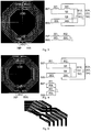
- Fig. 5 illustrates a detail of a layout of windings of a tunable inductor arrangement according to an embodiment.
- Crossings of conductive lanes forming the windings can thus be achieved.
- Two or more of the winding parts can be arranged in a plurality of conductive layers on the chip or substrate.
- the lanes are provided side by side on the substrate and the crossings using layered conductors.
- the lanes can also use layered conductors and be placed on top of each other, or a combination of be provided in different layers and side by side.
- the shape of the windings have also been illustrated as an octagon, but other shapes are as feasible, such as circular, square, or other n-sided shape, where n is 3 or higher, or combinations thereof, which form windings enclosing a magnetic field which is the purpose of the windings to form an inductance.
- the inductance can be adapted for differential purposes or single-ended purposes in conventional way.
- Fig. 6 schematically illustrates a radio front end where the tunable inductor arrangements according to embodiments are applicable.
- a radio front end circuit used for example in a 3GPP LTE radio, a multitude of bands may be used. Further, if for example carrier aggregation where separate bands are collected and used simultaneously in different configurations, versatility is a key to a feasible front end solution. Still further, if the front end should be usable for other radio access technologies as well, such as GSM, UMTS, WLAN, GNSS, etc., the demands on versatility further increases.
- the received signal can thus be in a multitude of frequencies and having wide or narrow bandwidth, and for example a band selection filter, or other circuit that need a resonator, may need to be configurable for this depending on current operating mode.
- Variable capacitance in such band selection filters normally do a lot, e.g. by using capacitor banks where capacitance can be switched in on demand, but by using a tunable inductor as demonstrated above, versatility can be improved, as well as performance of circuits including resonators.
- the expanded tunability of the filters can make the band selection filter usable for any band of the multi-band receiver.
- the demands on versatility can be met. Flexible band combinations are thereby enabled.
- the receiver 600 comprises a first receiver path arranged to receive a radio signal in a first frequency band and a second receiver path arranged to receive a radio signal in a second frequency band, wherein the first frequency band operates at a higher frequency than the second frequency band, i.e. a high-low band arrangement where both the high and the low bands can be received simultaneously.
- Each of the first and second receiver paths can be arranged to selectively operate at a selected frequency band among a plurality of frequency bands, e.g.
- the first high-band path can select to operate in one of 1800 MHz, 1900 MHz, 2100 MHz and 2700 MHz frequency bands while the second low-band path can select to operate in one of 750 MHz, 850 MHz, 900 MHz and 1500 MHz frequency bands simultaneously.
- These frequency bands are only demonstrated as examples, and other frequency bands and groupings between high and low frequency bands are equally possible.
- Each receiver path comprises a resonator comprising a tunable inductor arrangement 602, 604 as demonstrated above, wherein the resonators are arranged to be tuned for the selected frequency band in respective receiver path. Arrangements with more than two such receiver paths are also possible. Flexible frequency band combinations are thus enabled, which for example is advantageous in carrier aggregation solutions since each filter can be enabled to cover any frequency within the total frequency range of the receiver 600 due to the improved tenability of the filters.
- Fig. 6 illustrates an example where the resonator when used for tuning LNA output.
- the resonator with tunable inductor arrangement can of course be used for other purposes as well, such as for filters, impedance matching, etc, where a tunable inductance can be used.
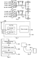
- Fig. 7 is a block diagram schematically illustrating communication device 700 according to an embodiment.
- the communication device comprises a receiver or transceiver 702, which can be connected to an antenna 704, and other circuits 706 such as a processor arranged interact with the receiver or transceiver 702, input and output interfaces of the communication device 700, etc.
- the receiver or transceiver 702 comprises a resonator 710, wherein the resonator comprises one or more tunable inductor arrangements according to any one of embodiments demonstrated above.
- the tunable inductor arrangement is tunable to enable the resonator 710 to work at a plurality of resonating frequencies.
- the receiver or transceiver can also comprise a controller 708 which can be arranged to control the tuning of the resonator 710, i.e. also the tunable inductor arrangement.
- the receiver 702 can for example be the multiband radio frequency receiver 600 demonstrated with reference to Fig. 6 .
- Fig. 8 is a flow chart schematically illustrating a method of a tunable inductor arrangement according to an embodiment.
- the method comprises determining 801 a tuning setting for the tunable inductor arrangement. This can be made by receiving frequency allocation from a remote entity or from an entity within a communication apparatus having the tunable inductor arrangement. Based on for example the frequency allocation information switch states are assigned 802 for the switch or respective switches for the tuning setting, and controlling 803 the switches according to the assigned switch states. Upon a new allocation, the procedure can be repeated.
- the method according to the present invention is suitable for implementation with aid of processing means, such as computers and/or processors, especially for the case where a digital controller controls the transceiver. Therefore, there is provided computer programs, comprising instructions arranged to cause the processing means, processor, or computer to perform the steps of any of the methods according to any of the embodiments described with reference to Fig. 8 .
- the computer programs preferably comprises program code which is stored on a computer readable medium 900, as illustrated in Fig. 9 , which can be loaded and executed by a processing means, processor, or computer 902 to cause it to perform the methods, respectively, according to embodiments of the present invention, preferably as any of the embodiments described with reference to Fig. 8 .
- the computer 902 and computer program product 900 can be arranged to execute the program code sequentially where actions of the any of the methods are performed stepwise.
- the processing means, processor, or computer 1002 is preferably what normally is referred to as an embedded system.
- the depicted computer readable medium 900 and computer 902 in Fig. 9 should be construed to be for illustrative purposes only to provide understanding of the principle, and not to be construed as any direct illustration of the elements.
Description
- The present invention generally relates to a tunable inductor arrangement, a radio frequency transceiver with a resonator having such an arrangement, a method of tuning the arrangement and a computer program for tuning.
- As more bands are to be supported in radio transceivers, which bands may span over a wide frequency range such as from 600MHz to 3800 MHz, this can be met by a set of resonators. It is known that tuning an LC (inductor-capacitor) resonator more than one octave is difficult, which gives that a multitude of resonators may be demanded. This problem is further emphasized when carrier aggregation, i.e. the communication is performed on several different carriers simultaneously, which carriers may be spread anywhere in the wide frequency range.
- LC resonators consume chip space, when implemented on-chip, and are fairly costly when implemented off-chip. It is therefore a desire to provide more flexible resonators.
- US patent application
US 2012/0286889 A1 discloses a reconfigurable network for a voltage-controlled oscillator. The reconfigurable network comprises a plurality of capacitors, a plurality of inductors and a plurality of switches. The plurality of capacitors, inductors and switches collectively form a resonance LC tank circuit. -
WO 03/052780 A1 -
WO 2007/006867 A1 discloses that the inductance of a monolithic planar inductor is distributed into smaller inductor portions (L11, L21, L22, L12). The smaller inductor portions (L11, L21, L22, L12) are provided in a cascade configuration in a manner that causes inductor to function as a differential inductor device. Some of the inductor portions are arranged to be symmetrically by-passed or shortcut (S1) in relation to the common point in one or more steps for operation in one or more higher radio frequency band. By means of the switchable symmetric shortcut, a controllable inductance step can be provided. The common-mode signal is affected the same inductance regardless of the controlled condition. - An object of the invention is to at least alleviate the above stated problem. The present invention is based on the understanding that both capacitance and inductance of an LC resonator need to be tuned to achieve the desired flexibility. A tunable inductor arrangement is provided accordingly. The inventor has also realized the demands that the self-resonant frequency need to be set high enough for high-frequency modes, the Q-value has to be high enough not to degrade gain or increase current consumption in a usable implementation, and that the ratio of the inductances need to be high enough to also cover the low bands. This is achieved by a switch arrangement in the tunable inductor arrangement which performs signal routing such that insertion loss is decreased.
- According to a first aspect, there is provided a tunable inductor arrangement arrangable on a chip or substrate. The tunable inductor comprises a first winding part connected at one end to a first input of the tunable inductor arrangement; a second winding part connected at one end to the other end of the first winding part; a third winding part connected at one end to a second input of the tunable inductor winding part connected at a first end to a second input of the tunable inductor arrangement; a fourth winding part connected at a first end to a second end of the third winding part; and a switch arrangement arranged to tune the tunable inductor arrangement by selectively provide any of a circuit comprising the first and fourth winding parts in parallel and the second and third winding parts in parallel, with the parallel couplings connected in series between the first and second inputs; and a circuit comprising the first, second, fourth and third winding parts in series between the first and second inputs.
- The switch arrangement may comprise a first switch connected between a second end of the second winding part and a virtual ground; a second switch connected between the second end of the fourth winding part and the virtual ground; a third switch connected between the first end of the second winding part and the virtual ground; a fourth switch connected between the first end of the fourth winding part and the virtual ground; a fifth switch connected between the first input and a second end of the fourth winding part; and a sixth switch connected between the second input and the second end of the second winding part. The tunable inductor arrangement may then be tunable by either closing the third, fourth, fifth and sixth switches and having the first and second switches open, or closing the first and second switches and having the third, fourth, fifth and sixth switches open.
- The switch arrangement may comprise a first switch connected between a second end of the second winding part and a second end of the fourth winding part; a second switch connected between the second end of the first winding part and the second end of the third winding part; a third switch connected between the first input and the second end of the fourth winding part; and a fourth switch connected between the second input and the second end of the second winding part. The tunable inductor arrangement may then be tunable by either closing the second, third and fourth switches and having the first switch open, or closing the first switch and having the second, third and fourth switches open.
- The first, second, third and fourth winding parts may be interleaved on the chip or substrate such that magnetic fields of the windings are essentially common.
- The tunable inductor arrangement may comprise a further winding part wherein the further winding part is arranged to cancel electro-magnetic coupling with the first to fourth winding parts.
- Two or more of the winding parts may be arranged in a plurality of conductive layers on the chip or substrate.
- The virtual ground may be a DC power supply, which at AC, such as radio frequency, acts as a ground for AC signals, or be a ground or DC reference voltage node.
- According to a second aspect, there is provided a radio frequency transceiver comprising a resonator, wherein the resonator comprises a tunable inductor arrangement according to the first aspect, wherein the tunable inductor arrangement is tunable to enable the resonator to selectably work at one of a plurality of resonating frequencies.
- According to a third aspect, there is provided a multiband radio frequency receiver comprising a first receiver path arranged to receive a radio signal in a first frequency band; a second receiver path arranged to receive a radio signal in a second frequency band, wherein the first frequency band operates at a higher frequency than the second frequency band, and each of the first and second receiver paths is arranged to selectively operate at a selected frequency band among a plurality of frequency bands; and comprises a resonator comprising a tunable inductor arrangement according to the first aspect, which resonator is arranged to be tuned for the selected frequency band.
- According to a fourth aspect, there is provided a communication device comprising a radio frequency transceiver according to the second aspect or a multiband radio frequency receiver according to the third aspect, and a processor arranged to interact with the radio frequency transceiver or multiband radio frequency receiver, wherein the processor is arranged to control to the switch arrangement to select a tuning mode of the tunable inductor arrangement.
- According to a fifth aspect, there is provided a method of a tunable inductor arrangement including winding parts and switches for tuning according to the first aspect. The method comprises determining a tuning setting for the tunable inductor arrangement; assigning switch states for respective switches for the tuning setting; and controlling the switches according to the assigned switch states.
- According to a sixth aspect, there is provided a computer program comprising computer executable instructions which when executed by a programmable controller of a radio frequency transceiver or multiband radio frequency receiver comprising a resonator which comprises a tunable inductor arrangement causes the controller to perform the method of the fifth aspect.
- Other objectives, features and advantages of the present invention will appear from the following detailed disclosure, from the attached dependent claims as well as from the drawings. Generally, all terms used in the claims are to be interpreted according to their ordinary meaning in the technical field, unless explicitly defined otherwise herein. All references to "a/an/the [element, device, component, means, step, etc]" are to be interpreted openly as referring to at least one instance of said element, device, component, means, step, etc., unless explicitly stated otherwise. The steps of any method disclosed herein do not have to be performed in the exact order disclosed, unless explicitly stated.
- The above, as well as additional objects, features and advantages of the present invention, will be better understood through the following illustrative and non-limiting detailed description of preferred embodiments of the present invention, with reference to the appended drawings.
-
Fig 1 schematically illustrates a tunable inductor arrangement according to an embodiment. -
Fig. 2 illustrates a layout of windings of a tunable inductor arrangement together with a schematic indication on the switch arrangement according to an embodiment. -
Fig. 3 illustrates a layout of windings of a tunable inductor arrangement when switches are in a first state, as illustrated in corresponding schematic to the right, according to an embodiment. -
Fig. 4 illustrates a layout of windings of a tunable inductor arrangement when switches are in a second state, as illustrated in corresponding schematic to the right, according to an embodiment. -
Fig. 5 illustrates a detail of a layout of windings of a tunable inductor arrangement according to an embodiment. -
Fig. 6 schematically illustrates a radio front end where the tunable inductor arrangements according to embodiments are applicable. -
Fig. 7 is a block diagram schematically illustrating a communication device according to an embodiment. -
Fig. 8 is a flow chart schematically illustrating a method of a tunable inductor arrangement according to an embodiment. -
Fig. 9 schematically illustrates a computer program and a processor for implementing the method. -
Fig 1 schematically illustrates a tunable inductor arrangement according to an embodiment. The inductor arrangement is preferably arranged on a chip or substrate, as will be demonstrated below. The tunable inductor arrangement comprises a first winding part W1 connected at one end to a first input INP of the tunable inductor arrangement, a second winding part W2 connected at one end to the other end of the first winding part W1, a third winding part W3 connected at one end to a second input INN of the tunable inductor arrangement and a fourth winding part W4 connected at one end to the other end of the third winding part. A switch arrangement is arranged to tune the tunable inductor arrangement by selectively provide for that a circuit comprising the first and fourth winding parts W1, W4 in parallel and the second and third winding part W2, W3 in parallel, and then couple the respective parallel couplings W1, W4; W2, W3 in series between the first and second inputs INP, INN, or a circuit comprising the first, second, fourth and third winding parts W1, W2, W4, W3 in series between the first and second inputs INP, INN. The switch arrangement comprises a first switch S1 connected between the other end of the second winding part W2 and a virtual ground VDD, a second switch S2 connected between the other end of the fourth winding part W4 and the virtual ground VDD. The virtual ground may be a DC power supply, thus here named VDD, which at AC, such as radio frequency, acts as a ground for AC signals, or be a ground or DC reference voltage node. If the centre tap is not used, the first and second switches can be substituted by a single switch S12 providing the same function as the first and second switches S1, S2. The switch arrangement further comprises a third switch S3 connected between the other end of the first winding part W1 and the virtual ground VDD, and a fourth switch S4 connected between the other end of the third winding part W3 and the virtual ground VDD. Similar, when the centre tap is not used, the third and fourth switches can be substituted by a single switch S34 providing the same function as the third and fourth switches S3, S4. The tunable inductor arrangement is thereby tunable by either closing the first and second switches S1, S2 (or the single switch S12) such that a circuit from the first input INP via the first winding part W1, the second winding part W2, the closed first switch S1, the closed second switch S2 (or the single switch S12), the fourth winding part W4 and the third winding part W3 to the second input INN is formed, i.e. all the windings W1-W4 are coupled in series. - To accomplish that all windings are operable in both modes, the switch arrangement further comprises a fifth switch S5 connected between the one end of the first winding part W1 and the other end of the fourth winding part W4, and a sixth switch S6 connected between the one end of the third winding part W3 and the other end of the second winding part W2. The tunable inductor arrangement is thereby further tunable by closing the fifth and sixth switches S5, S6 when the third and fourth switches S3, S4 are closed. In that case, a circuit is formed from the first input INP via the closed fifth switch S5, the fourth winding part W4, the closed fourth switch S4, the closed third switch S3, the second winding part W2, and the closed sixth switch S6 to the second input INN.
- Thereby, the tunable inductor arrangement is enabled to, by selectively provide for that a circuit comprising the first and fourth winding parts W1, W4 in parallel and the second and third winding part W2, W3 in parallel, and then couple the respective parallel couplings W1, W4; W2, W3 in series between the first and second inputs INP, INN, or a circuit comprising the first, second, fourth and third winding parts W1, W2, W4, W3 in series between the first and second inputs INP, INN, provide different inductances where all the windings are operable in both modes.
- Although the above demonstrated tunable inductor arrangement can operate all windings in all its operating modes, it may still be combinable with additional inductor arrangements which does not. Such combinations may provide further tunability. To achieve a good Q-value, all winding parts with mutual magnetic interaction are preferably in operation at all states. One or more circuits as the one demonstrated above can be used as building blocks to achieve a tunable inductor arrangement.
-
Fig. 2 illustrates a layout of windings of a tunable inductor arrangement together with a schematic indication on the switch arrangement according to an embodiment. The circuit corresponds to those demonstrated with reference toFig. 1 , and the function for providing different inductances is the same. -
Fig. 3 illustrates a layout of windings of a tunable inductor arrangement when switches are in a first state, as illustrated in corresponding schematic to the upper right, according to an embodiment. At lower right, the equivalent circuit is drawn for simple understanding of the effect of the circuit. The circuit corresponds to the one achieved by having the single switch S12 (or the first and second switches S1 and S2) ofFigs 1 and 2 closed and the other switches S34 (or S4, S4), S5, S6 open. Here, it can be seen that the series coupling provides a winding going from the terminal INP through all the conductive lanes and ending at the terminal INN. - The windings are arranged on a substrate or chip. The substrate can also be a printed circuit board. A virtual ground node can also be applied, which is also elucidated below with reference to
Fig. 4 . The virtual ground, which may be a DC power supply VDD, which at AC, such as radio frequency, acts as a ground for AC signals, or be a ground or DC reference voltage node, can be employed. When in the first state, the switch S12 (or S1, S2) connects the virtual ground node. -
Fig. 4 illustrates a layout of windings of a tunable inductor arrangement when switches are in a second state, as illustrated in corresponding schematic to the upper right, according to an embodiment. At lower right, the equivalent circuit is drawn for simple understanding of the effect of the circuit. The circuit corresponds to the one achieved by having the single switch S12 (or the first and second switches S1 and S2) ofFigs 1 and 2 open and the other switches closed. Here, it can be seen that a first parallel coupling starting from the terminal INP provides a winding going to meet a second parallel coupling at point A, which goes all the way to the terminal INN. At the coupling at point A, a virtual ground (not shown), such as power supply, can be connected. The virtual ground may be a DC power supply, which at AC, such as radio frequency, acts as a ground for AC signals, or be a ground or DC reference voltage node. When in the second state, the switch S34 (or S3, S4) connects the virtual ground node. As can be seen when consideringFigs 3 and 4 , the virtual ground node cannot be employed as a single centre tap in the layout of the windings as ofFigs 3 and 4 . However, for some layouts, i.e. where S12 (or S1, S2) and S34 (or S3, S4) are located adjacent to each other, which is depending on the number of turns and the application of the turns in multiple metal layers, the layout of the virtual ground node can be kept to one area of the substrate or chip. -
Fig. 5 illustrates a detail of a layout of windings of a tunable inductor arrangement according to an embodiment. Crossings of conductive lanes forming the windings can thus be achieved. Two or more of the winding parts can be arranged in a plurality of conductive layers on the chip or substrate. In the illustrations, the lanes are provided side by side on the substrate and the crossings using layered conductors. However, the lanes can also use layered conductors and be placed on top of each other, or a combination of be provided in different layers and side by side. The shape of the windings have also been illustrated as an octagon, but other shapes are as feasible, such as circular, square, or other n-sided shape, where n is 3 or higher, or combinations thereof, which form windings enclosing a magnetic field which is the purpose of the windings to form an inductance. The inductance can be adapted for differential purposes or single-ended purposes in conventional way. -
Fig. 6 schematically illustrates a radio front end where the tunable inductor arrangements according to embodiments are applicable. In a radio front end circuit used for example in a 3GPP LTE radio, a multitude of bands may be used. Further, if for example carrier aggregation where separate bands are collected and used simultaneously in different configurations, versatility is a key to a feasible front end solution. Still further, if the front end should be usable for other radio access technologies as well, such as GSM, UMTS, WLAN, GNSS, etc., the demands on versatility further increases. The received signal can thus be in a multitude of frequencies and having wide or narrow bandwidth, and for example a band selection filter, or other circuit that need a resonator, may need to be configurable for this depending on current operating mode. Variable capacitance in such band selection filters normally do a lot, e.g. by using capacitor banks where capacitance can be switched in on demand, but by using a tunable inductor as demonstrated above, versatility can be improved, as well as performance of circuits including resonators. For example, by using such resonators for band selection filters in multi-band receivers, the expanded tunability of the filters can make the band selection filter usable for any band of the multi-band receiver. By using one or moretunable inductor arrangements - An example where the front end arrangement as demonstrated above can be used is a multiband
radio frequency receiver 600. Thereceiver 600 comprises a first receiver path arranged to receive a radio signal in a first frequency band and a second receiver path arranged to receive a radio signal in a second frequency band, wherein the first frequency band operates at a higher frequency than the second frequency band, i.e. a high-low band arrangement where both the high and the low bands can be received simultaneously. Each of the first and second receiver paths can be arranged to selectively operate at a selected frequency band among a plurality of frequency bands, e.g. the first high-band path can select to operate in one of 1800 MHz, 1900 MHz, 2100 MHz and 2700 MHz frequency bands while the second low-band path can select to operate in one of 750 MHz, 850 MHz, 900 MHz and 1500 MHz frequency bands simultaneously. These frequency bands are only demonstrated as examples, and other frequency bands and groupings between high and low frequency bands are equally possible. Each receiver path comprises a resonator comprising atunable inductor arrangement receiver 600 due to the improved tenability of the filters. -
Fig. 6 illustrates an example where the resonator when used for tuning LNA output. The resonator with tunable inductor arrangement can of course be used for other purposes as well, such as for filters, impedance matching, etc, where a tunable inductance can be used. -
Fig. 7 is a block diagram schematically illustratingcommunication device 700 according to an embodiment. The communication device comprises a receiver ortransceiver 702, which can be connected to anantenna 704, andother circuits 706 such as a processor arranged interact with the receiver ortransceiver 702, input and output interfaces of thecommunication device 700, etc. The receiver ortransceiver 702 comprises aresonator 710, wherein the resonator comprises one or more tunable inductor arrangements according to any one of embodiments demonstrated above. The tunable inductor arrangement is tunable to enable theresonator 710 to work at a plurality of resonating frequencies. The receiver or transceiver can also comprise acontroller 708 which can be arranged to control the tuning of theresonator 710, i.e. also the tunable inductor arrangement. Thereceiver 702 can for example be the multibandradio frequency receiver 600 demonstrated with reference toFig. 6 . -
Fig. 8 is a flow chart schematically illustrating a method of a tunable inductor arrangement according to an embodiment. The method comprises determining 801 a tuning setting for the tunable inductor arrangement. This can be made by receiving frequency allocation from a remote entity or from an entity within a communication apparatus having the tunable inductor arrangement. Based on for example the frequency allocation information switch states are assigned 802 for the switch or respective switches for the tuning setting, and controlling 803 the switches according to the assigned switch states. Upon a new allocation, the procedure can be repeated. - The method according to the present invention is suitable for implementation with aid of processing means, such as computers and/or processors, especially for the case where a digital controller controls the transceiver. Therefore, there is provided computer programs, comprising instructions arranged to cause the processing means, processor, or computer to perform the steps of any of the methods according to any of the embodiments described with reference to
Fig. 8 . The computer programs preferably comprises program code which is stored on a computerreadable medium 900, as illustrated inFig. 9 , which can be loaded and executed by a processing means, processor, orcomputer 902 to cause it to perform the methods, respectively, according to embodiments of the present invention, preferably as any of the embodiments described with reference toFig. 8 . Thecomputer 902 andcomputer program product 900 can be arranged to execute the program code sequentially where actions of the any of the methods are performed stepwise. The processing means, processor, or computer 1002 is preferably what normally is referred to as an embedded system. Thus, the depicted computerreadable medium 900 andcomputer 902 inFig. 9 should be construed to be for illustrative purposes only to provide understanding of the principle, and not to be construed as any direct illustration of the elements. - The invention has mainly been described above with reference to a few embodiments. However, as is readily appreciated by a person skilled in the art, other embodiments than the ones disclosed above are equally possible within the scope of the invention, as defined by the appended patent claims.
Claims (11)
- A tunable inductor arrangement arrangeable on a chip or substrate, the tunable inductor comprising
a first winding part (W1) connected at one end to a first input (INP) of the tunable inductor arrangement;
a second winding part (W2) connected at one end to the other end of the first winding part (W1);
a third winding part (W3) connected at one end to a second input (INN) of the tunable inductor arrangement;
a fourth winding part (W4) connected at one end to the other end of the third winding part (W3);
wherein the first, second, third and fourth winding parts (W1-W4) are interleaved on the chip or substrate such that magnetic fields of the windings (W1-W4) are common; and
a switch arrangement arranged to tune the tunable inductor arrangement to selectively provide eithera circuit comprising the first and fourth winding parts (W1, W4) in parallel and the second and third winding parts (W2, W3) in parallel, with the parallel couplings (W1, W4; W2, W3) connected in series between the first and second inputs (INP, INN); ora circuit comprising the first, second, fourth and third winding parts (W1-W4) in series between the first and second inputs (INP, INN). - The tunable inductor arrangement of claim 1 wherein the switch arrangement comprises
a first switch (S1) connected between the other end of the second winding part (W2) and a virtual ground (VDD);
a second switch (S2) connected between the other end of the fourth winding part (W4) and the virtual ground (VDD);
a third switch (S3) connected between the other end of the first winding part (W1) and the virtual ground (VDD);
a fourth switch (S4) connected between the other end of the third winding part (W3) and the virtual ground (VDD);
a fifth switch (S5) connected between the first input (INP) and the other end of the fourth winding part (W4); and
a sixth switch (S6) connected between the second input (INN) and the other end of the second winding part (W2),
wherein the tunable inductor arrangement is tunable by either closing the third, fourth, fifth and sixth switches (S3-S6) and having the first and second switches (S1, S2) open, or closing the first and second switches (S1, S2) and having the third, fourth, fifth and sixth switches (S3-S6) open. - The tunable inductor arrangement of claim 1 wherein the switch arrangement comprises
a first switch (S12) connected between the other end of the second winding part (W2) and the other end of the fourth winding part (W4);
a second switch (S34) connected between the other end of the first winding part (W1) and the other end of the third winding part (W3);
a third switch (S5) connected between the first input (INP) and the other end of the fourth winding part; and
a fourth switch (S6) connected between the second input (INN) and the other end of the second winding part,
wherein the tunable inductor arrangement is tunable by either closing the second, third and fourth switches (S34, S5, S6) and having the first switch (S12) open, or closing the first switch (S12) and having the second, third and fourth switches (S34, S5, S6) open. - The tunable inductor arrangement of any one of claims 1 to 3, comprising a further winding part wherein the further winding part is arranged to cancel electro-magnetic coupling with the first to fourth winding parts.
- The tunable inductor arrangement of any one of claims 1 to 4, wherein two or more of the winding parts are arranged in a plurality of conductive layers on the chip or substrate.
- A radio frequency transceiver (702) comprising a resonator (710), wherein the resonator (710) comprises a tunable inductor arrangement according to any one of claims 1 to 5, wherein the tunable inductor arrangement is tunable to enable the resonator (710) to selectably work at one of a plurality of resonating frequencies.
- A multiband radio frequency receiver (600) comprising a first receiver path arranged to receive a radio signal in a first frequency band; a second receiver path arranged to receive a radio signal in a second frequency band,
wherein the first frequency band operates at a higher frequency than the second frequency band, and each of the first and second receiver pathsis arranged to selectively operate at a selected frequency band among a plurality of frequency bands; andcomprises a resonator comprising a tunable inductor arrangement (602, 604) according to any one of claims 1 to 5, which resonator is arranged to be tuned for the selected frequency band. - A communication device (700) comprising a radio frequency transceiver (702) according to claim 6 or a multiband radio frequency receiver (702) according to claim 7, and a processor (708) arranged to interact with the radio frequency transceiver or multiband radio frequency receiver (702), wherein the processor (708) is arranged to control the switch arrangement to select a tuning mode of the tunable inductor arrangement.
- A method for tuning of a tunable inductor arrangement including winding parts and switches according to any one of claims 1 to 5, the method comprises
determining (801) a tuning setting for the tunable inductor arrangement; assigning (802) switch states for respective switches for the tuning setting; and controlling (803) the switches according to the assigned switch states. - A method according to claim 9 wherein a computer program comprises computer executable instructions which when executed by a programmable controller (708, 902) of a radio frequency transceiver (702) or multiband radio frequency receiver (600) comprising a resonator (710) which comprises a tunable inductor arrangement causes the controller (708, 902) to perform the method.
- A computer program product comprising a computer readable medium, having thereon a computer program comprising program instructions, the computer program being loadable into a data-processing unit and adapted to cause execution of the method according to claim 9 when the computer program is run by the data-processing unit.
Priority Applications (20)
| Application Number | Priority Date | Filing Date | Title |
|---|---|---|---|
| PL13188910T PL2863428T3 (en) | 2013-10-16 | 2013-10-16 | Tunable inductor arrangement, transceiver, method and computer program |
| HUE17167101A HUE052115T2 (en) | 2013-10-16 | 2013-10-16 | Transceiver, receiver and communication device with switch arrangement |
| ES13188910.7T ES2637119T3 (en) | 2013-10-16 | 2013-10-16 | Tunable inductor arrangement, transceiver, procedure and computer program |
| EP13188910.7A EP2863428B1 (en) | 2013-10-16 | 2013-10-16 | Tunable inductor arrangement, transceiver, method and computer program |
| EP17167101.9A EP3220419B1 (en) | 2013-10-16 | 2013-10-16 | Transceiver, receiver and communication device with switch arrangement |
| BR122020020407-9A BR122020020407B1 (en) | 2013-10-16 | 2014-10-10 | CHIP HAVING A TUNEABLE INDUCER ARRANGEMENT, RADIO FREQUENCY TRANSCEPTOR, MULTI-BAND RADIO FREQUENCY RECEIVER, AND, COMMUNICATION DEVICE |
| US15/029,284 US9905350B2 (en) | 2013-10-16 | 2014-10-10 | Tunable inductor arrangement, transceiver, method and computer program |
| CN201480057042.7A CN105659380B (en) | 2013-10-16 | 2014-10-10 | Tunable inductor device, transceiver, method and computer program |
| NZ718482A NZ718482A (en) | 2013-10-16 | 2014-10-10 | Tunable inductor arrangement, transceiver, method and computer program |
| AP2016009134A AP2016009134A0 (en) | 2013-10-16 | 2014-10-10 | Tunable inductor arrangement, transceiver, method and computer program |
| RU2016118419A RU2639600C2 (en) | 2013-10-16 | 2014-10-10 | Adjustable inductor circuit, transceiver, method and computer program |
| KR1020167012482A KR101893273B1 (en) | 2013-10-16 | 2014-10-10 | Tunable inductor arrangement, transceiver, method and computer program |
| PCT/EP2014/071750 WO2015055527A1 (en) | 2013-10-16 | 2014-10-10 | Tunable inductor arrangement, transceiver, method and computer program |
| CN201810770242.7A CN108899158B (en) | 2013-10-16 | 2014-10-10 | Tunable inductor arrangement, transceiver, method and computer program |
| KR1020187023711A KR102002268B1 (en) | 2013-10-16 | 2014-10-10 | Tunable inductor arrangement, transceiver, method and computer program |
| BR112016008244-3A BR112016008244B1 (en) | 2013-10-16 | 2014-10-10 | TUNTABLE INDUCER ARRANGEMENT, RADIO FREQUENCY TRANSCEPTOR, MULTI-BAND RADIO FREQUENCY RECEIVER, COMMUNICATION DEVICE, AND, METHOD FOR TUNING A TUNTABLE INDUCER ARRANGEMENT |
| US15/872,184 US10283252B2 (en) | 2013-10-16 | 2018-01-16 | Tunable inductor arrangement, transceiver, method and computer program |
| US16/360,414 US10892080B2 (en) | 2013-10-16 | 2019-03-21 | Tunable inductor arrangement, transceiver, method, and computer program |
| US17/118,212 US11527347B2 (en) | 2013-10-16 | 2020-12-10 | Tunable inductor arrangement, transceiver, method and computer program |
| US17/986,435 US11923119B2 (en) | 2013-10-16 | 2022-11-14 | Tunable inductor arrangement, transceiver, method, and computer program |
Applications Claiming Priority (1)
| Application Number | Priority Date | Filing Date | Title |
|---|---|---|---|
| EP13188910.7A EP2863428B1 (en) | 2013-10-16 | 2013-10-16 | Tunable inductor arrangement, transceiver, method and computer program |
Related Child Applications (1)
| Application Number | Title | Priority Date | Filing Date |
|---|---|---|---|
| EP17167101.9A Division EP3220419B1 (en) | 2013-10-16 | 2013-10-16 | Transceiver, receiver and communication device with switch arrangement |
Publications (2)
| Publication Number | Publication Date |
|---|---|
| EP2863428A1 EP2863428A1 (en) | 2015-04-22 |
| EP2863428B1 true EP2863428B1 (en) | 2017-05-17 |
Family
ID=49356319
Family Applications (2)
| Application Number | Title | Priority Date | Filing Date |
|---|---|---|---|
| EP13188910.7A Active EP2863428B1 (en) | 2013-10-16 | 2013-10-16 | Tunable inductor arrangement, transceiver, method and computer program |
| EP17167101.9A Active EP3220419B1 (en) | 2013-10-16 | 2013-10-16 | Transceiver, receiver and communication device with switch arrangement |
Family Applications After (1)
| Application Number | Title | Priority Date | Filing Date |
|---|---|---|---|
| EP17167101.9A Active EP3220419B1 (en) | 2013-10-16 | 2013-10-16 | Transceiver, receiver and communication device with switch arrangement |
Country Status (12)
| Country | Link |
|---|---|
| US (5) | US9905350B2 (en) |
| EP (2) | EP2863428B1 (en) |
| KR (2) | KR102002268B1 (en) |
| CN (2) | CN108899158B (en) |
| AP (1) | AP2016009134A0 (en) |
| BR (1) | BR112016008244B1 (en) |
| ES (1) | ES2637119T3 (en) |
| HU (1) | HUE052115T2 (en) |
| NZ (1) | NZ718482A (en) |
| PL (1) | PL2863428T3 (en) |
| RU (1) | RU2639600C2 (en) |
| WO (1) | WO2015055527A1 (en) |
Cited By (2)
| Publication number | Priority date | Publication date | Assignee | Title |
|---|---|---|---|---|
| US10249426B2 (en) | 2013-10-16 | 2019-04-02 | Telefonaktiebolaget Lm Ericsson (Publ) | Tunable inductor arrangement, transceiver, method and computer program |
| US10283252B2 (en) | 2013-10-16 | 2019-05-07 | Telefonaktiebolaget Lm Ericsson (Publ) | Tunable inductor arrangement, transceiver, method and computer program |
Families Citing this family (6)
| Publication number | Priority date | Publication date | Assignee | Title |
|---|---|---|---|---|
| TWI664649B (en) * | 2017-07-31 | 2019-07-01 | 瑞昱半導體股份有限公司 | Inductor device |
| US10447204B2 (en) | 2017-09-15 | 2019-10-15 | Qualcomm Incorporated | Switchable inductor network for wideband circuits |
| US10381981B2 (en) | 2017-09-15 | 2019-08-13 | Qualcomm Incorporated | Degeneration for a wideband voltage-controlled oscillator |
| EP3618109B1 (en) | 2018-08-28 | 2021-11-17 | Nxp B.V. | Integrated passive coupler and method |
| CN110166020B (en) * | 2019-05-31 | 2020-04-24 | 厦门市三安集成电路有限公司 | Filter and duplexer |
| WO2021102812A1 (en) * | 2019-11-28 | 2021-06-03 | 华为技术有限公司 | Inductors, oscillators and terminal device |
Family Cites Families (50)
| Publication number | Priority date | Publication date | Assignee | Title |
|---|---|---|---|---|
| NL8602033A (en) | 1986-08-08 | 1988-03-01 | Nedap Nv | PRECISION FOCUS ON RECOGNITION SYSTEM. |
| DE3817726A1 (en) | 1988-05-25 | 1989-11-30 | Siemens Ag | DEVICE FOR SPACIOUS ULTRASONIC LOCATION OF CONCRETE |
| US5351688A (en) | 1993-08-16 | 1994-10-04 | Univ. Of Ne Board Of Regents | NMR quadrature detection solenoidal coils |
| JPH0935942A (en) * | 1995-07-20 | 1997-02-07 | Kokusai Electric Co Ltd | Step variable inductor |
| FR2812445B1 (en) * | 2000-07-31 | 2002-11-29 | St Microelectronics Sa | INTEGRATED STRUCTURE OF SHARED VALUE INDUCTANCES ON A SEMICONDUCTOR SUBSTRATE |
| US6549071B1 (en) * | 2000-09-12 | 2003-04-15 | Silicon Laboratories, Inc. | Power amplifier circuitry and method using an inductance coupled to power amplifier switching devices |
| US6549096B2 (en) * | 2001-03-19 | 2003-04-15 | International Business Machines Corporation | Switched inductor/varactor tuning circuit having a variable integrated inductor |
| GB0126219D0 (en) * | 2001-11-01 | 2002-01-02 | Koninkl Philips Electronics Nv | Tunable filter |
| US7005930B1 (en) | 2001-11-14 | 2006-02-28 | Berkana Wireless, Inc. | Synchronously coupled oscillator |
| DE10162263A1 (en) * | 2001-12-18 | 2003-07-10 | Infineon Technologies Ag | Inductive component |
| US6621365B1 (en) | 2002-04-03 | 2003-09-16 | Nokia Corporation | Method and apparatus providing a dual mode VCO for an adaptive receiver |
| JP2004303851A (en) * | 2003-03-31 | 2004-10-28 | Japan Ae Power Systems Corp | Device and method for tap-changing connection method of mobile transformer |
| US7151430B2 (en) | 2004-03-03 | 2006-12-19 | Telefonaktiebolaget Lm Ericsson (Publ) | Method of and inductor layout for reduced VCO coupling |
| US6982887B2 (en) | 2004-04-26 | 2006-01-03 | Astec International Limited | DC-DC converter with coupled-inductors current-doubler |
| US7432794B2 (en) | 2004-08-16 | 2008-10-07 | Telefonaktiebolaget L M Ericsson (Publ) | Variable integrated inductor |
| TW200633362A (en) | 2004-11-15 | 2006-09-16 | Koninkl Philips Electronics Nv | Variable inductance circuitry for frequency control of a voltage controlled oscillator |
| FI20055402A0 (en) * | 2005-07-11 | 2005-07-11 | Nokia Corp | Inductor for multi-band radio frequency operation |
| US8219060B2 (en) | 2006-07-28 | 2012-07-10 | Qualcomm Incorporated | Dual inductor circuit for multi-band wireless communication device |
| CN101188159B (en) * | 2006-11-24 | 2011-01-12 | 阎跃军 | Segment adjustable inductor |
| US7649407B2 (en) * | 2007-09-28 | 2010-01-19 | Intel Corporation | Digitally tuned, integrated RF filters with enhanced linearity for multi-band radio applications |
| US7688158B2 (en) * | 2007-09-28 | 2010-03-30 | Intel Corporation | Digitally tuned, integrated baluns with enhanced linearity for multi-band radio applications |
| US7808310B2 (en) | 2007-11-28 | 2010-10-05 | Infineon Technologies, Ag | Differential band-pass filter having symmetrically interwoven inductors |
| WO2009081342A1 (en) | 2007-12-21 | 2009-07-02 | Nxp B.V. | Low magnetic field inductor |
| US8237531B2 (en) | 2007-12-31 | 2012-08-07 | Globalfoundries Singapore Pte. Ltd. | Tunable high quality factor inductor |
| JPWO2009119042A1 (en) | 2008-03-28 | 2011-07-21 | パナソニック株式会社 | Voltage-controlled oscillator, PLL circuit using the same, and wireless communication device |
| US8183971B2 (en) | 2008-04-10 | 2012-05-22 | Nxp B.V. | 8-shaped inductor |
| JP2009260080A (en) | 2008-04-17 | 2009-11-05 | Fujitsu Ltd | Inductor device |
| US7953462B2 (en) * | 2008-08-04 | 2011-05-31 | Vartanian Harry | Apparatus and method for providing an adaptively responsive flexible display device |
| US7821372B2 (en) | 2008-12-31 | 2010-10-26 | Taiwan Semiconductor Manufacturing Co., Ltd. | On-chip transformer BALUN structures |
| US8291422B2 (en) * | 2009-05-11 | 2012-10-16 | Bbn Technologies Corp. | Energy-aware computing environment scheduler |
| JP2010272815A (en) * | 2009-05-25 | 2010-12-02 | Renesas Electronics Corp | Variable inductor |
| EP2273613A1 (en) | 2009-07-07 | 2011-01-12 | Nxp B.V. | Magnetic shield layout, semiconductor device and application |
| US8842410B2 (en) * | 2009-08-31 | 2014-09-23 | Qualcomm Incorporated | Switchable inductor network |
| JP5446671B2 (en) | 2009-09-29 | 2014-03-19 | ソニー株式会社 | Wireless transmission system and wireless communication method |
| RU92273U1 (en) | 2009-10-27 | 2010-03-10 | ОАО Российский институт мощного радиостроения | RADIO TRANSMISSION DEVICE |
| WO2011073853A1 (en) | 2009-12-17 | 2011-06-23 | Stmicroelectronics S.R.L. | Circuit arrangement of a voltage controlled oscillator |
| EP2337150B1 (en) | 2009-12-18 | 2012-12-05 | Laird Technologies AB | An antenna arrangement and a portable radio communication device comprising such an antenna arrangement |
| US20120244802A1 (en) * | 2011-03-24 | 2012-09-27 | Lei Feng | On chip inductor |
| US20120286889A1 (en) * | 2011-05-10 | 2012-11-15 | Samsung Electro-Mechanics Company | Systems and Methods for Wideband CMOS Voltage-Controlled Oscillators Using Reconfigurable Inductor Arrays |
| US9002309B2 (en) | 2011-05-27 | 2015-04-07 | Qualcomm Incorporated | Tunable multi-band receiver |
| US8699974B2 (en) | 2011-08-24 | 2014-04-15 | Aviacomm Inc. | Wideband transmitter front-end |
| CN102306642A (en) * | 2011-09-22 | 2012-01-04 | 华东师范大学 | On-chip integrated inductor with adjustable inductance value |
| US8742859B2 (en) * | 2011-12-06 | 2014-06-03 | Qualcomm Incorporated | Tunable inductor circuit |
| US8639286B2 (en) | 2011-12-23 | 2014-01-28 | Broadcom Corporation | RF transmitter having broadband impedance matching for multi-band application support |
| EP2648193B1 (en) | 2012-04-03 | 2015-07-29 | Telefonaktiebolaget L M Ericsson (publ) | An inductor layout, and a voltage-controlled oscillator (VCO) system |
| US20140028521A1 (en) | 2012-07-27 | 2014-01-30 | Rf Micro Devices, Inc. | Tuner topology for wide bandwidth |
| US9058130B2 (en) * | 2013-02-05 | 2015-06-16 | International Business Machines Corporation | Tunable sector buffer for wide bandwidth resonant global clock distribution |
| US9276547B2 (en) * | 2013-06-28 | 2016-03-01 | Peregrine Semiconductor Corporation | Systems and methods of stacking LC tanks for wide tuning range and high voltage swing |
| DK2863429T3 (en) | 2013-10-16 | 2017-09-04 | ERICSSON TELEFON AB L M (publ) | Adjustable inductor device, transceiver, method and computer program |
| EP2863428B1 (en) * | 2013-10-16 | 2017-05-17 | Telefonaktiebolaget LM Ericsson (publ) | Tunable inductor arrangement, transceiver, method and computer program |
-
2013
- 2013-10-16 EP EP13188910.7A patent/EP2863428B1/en active Active
- 2013-10-16 ES ES13188910.7T patent/ES2637119T3/en active Active
- 2013-10-16 PL PL13188910T patent/PL2863428T3/en unknown
- 2013-10-16 EP EP17167101.9A patent/EP3220419B1/en active Active
- 2013-10-16 HU HUE17167101A patent/HUE052115T2/en unknown
-
2014
- 2014-10-10 WO PCT/EP2014/071750 patent/WO2015055527A1/en active Application Filing
- 2014-10-10 US US15/029,284 patent/US9905350B2/en active Active
- 2014-10-10 CN CN201810770242.7A patent/CN108899158B/en active Active
- 2014-10-10 AP AP2016009134A patent/AP2016009134A0/en unknown
- 2014-10-10 CN CN201480057042.7A patent/CN105659380B/en active Active
- 2014-10-10 BR BR112016008244-3A patent/BR112016008244B1/en active IP Right Grant
- 2014-10-10 KR KR1020187023711A patent/KR102002268B1/en active IP Right Grant
- 2014-10-10 RU RU2016118419A patent/RU2639600C2/en active
- 2014-10-10 KR KR1020167012482A patent/KR101893273B1/en active IP Right Grant
- 2014-10-10 NZ NZ718482A patent/NZ718482A/en unknown
-
2018
- 2018-01-16 US US15/872,184 patent/US10283252B2/en active Active
-
2019
- 2019-03-21 US US16/360,414 patent/US10892080B2/en active Active
-
2020
- 2020-12-10 US US17/118,212 patent/US11527347B2/en active Active
-
2022
- 2022-11-14 US US17/986,435 patent/US11923119B2/en active Active
Cited By (9)
| Publication number | Priority date | Publication date | Assignee | Title |
|---|---|---|---|---|
| US10249426B2 (en) | 2013-10-16 | 2019-04-02 | Telefonaktiebolaget Lm Ericsson (Publ) | Tunable inductor arrangement, transceiver, method and computer program |
| US10283252B2 (en) | 2013-10-16 | 2019-05-07 | Telefonaktiebolaget Lm Ericsson (Publ) | Tunable inductor arrangement, transceiver, method and computer program |
| EP3220419B1 (en) * | 2013-10-16 | 2020-07-08 | Telefonaktiebolaget LM Ericsson (publ) | Transceiver, receiver and communication device with switch arrangement |
| US10892080B2 (en) | 2013-10-16 | 2021-01-12 | Telefonaktiebolaget Lm Ericsson (Publ) | Tunable inductor arrangement, transceiver, method, and computer program |
| US10916364B2 (en) | 2013-10-16 | 2021-02-09 | Telefonaktiebolaget Lm Ericsson (Publ) | Tunable inductor arrangement, transceiver, method and computer program |
| US11456102B2 (en) | 2013-10-16 | 2022-09-27 | Telefonaktiebolaget Lm Ericsson (Publ) | Tunable inductor arrangement, transceiver, method and computer program |
| US11527347B2 (en) | 2013-10-16 | 2022-12-13 | Telefonaktiebolaget Lm Ericsson (Publ) | Tunable inductor arrangement, transceiver, method and computer program |
| US11854728B2 (en) | 2013-10-16 | 2023-12-26 | Telefonaktiebolaget Lm Ericsson (Publ) | Tunable inductor arrangement, transceiver, method and computer program |
| US11923119B2 (en) | 2013-10-16 | 2024-03-05 | Telefonaktiebolaget Lm Ericsson (Publ) | Tunable inductor arrangement, transceiver, method, and computer program |
Also Published As
| Publication number | Publication date |
|---|---|
| WO2015055527A1 (en) | 2015-04-23 |
| CN108899158B (en) | 2021-03-12 |
| NZ718482A (en) | 2017-08-25 |
| EP3220419B1 (en) | 2020-07-08 |
| KR102002268B1 (en) | 2019-07-19 |
| US20160254084A1 (en) | 2016-09-01 |
| US11923119B2 (en) | 2024-03-05 |
| EP2863428A1 (en) | 2015-04-22 |
| CN108899158A (en) | 2018-11-27 |
| AP2016009134A0 (en) | 2016-04-30 |
| CN105659380A (en) | 2016-06-08 |
| US11527347B2 (en) | 2022-12-13 |
| EP3220419A1 (en) | 2017-09-20 |
| CN105659380B (en) | 2018-08-10 |
| US20210098169A1 (en) | 2021-04-01 |
| US10892080B2 (en) | 2021-01-12 |
| US20180204660A1 (en) | 2018-07-19 |
| BR112016008244A2 (en) | 2017-08-01 |
| KR20160072156A (en) | 2016-06-22 |
| US20230070802A1 (en) | 2023-03-09 |
| ES2637119T3 (en) | 2017-10-10 |
| HUE052115T2 (en) | 2021-04-28 |
| PL2863428T3 (en) | 2017-10-31 |
| KR20180096813A (en) | 2018-08-29 |
| BR112016008244B1 (en) | 2022-08-02 |
| US20190214176A1 (en) | 2019-07-11 |
| US10283252B2 (en) | 2019-05-07 |
| US9905350B2 (en) | 2018-02-27 |
| RU2016118419A (en) | 2017-11-21 |
| RU2639600C2 (en) | 2017-12-21 |
| KR101893273B1 (en) | 2018-08-29 |
Similar Documents
| Publication | Publication Date | Title |
|---|---|---|
| US11854728B2 (en) | Tunable inductor arrangement, transceiver, method and computer program | |
| US11923119B2 (en) | Tunable inductor arrangement, transceiver, method, and computer program | |
| ES2644019T3 (en) | Mesh made of wire rings and mesh making method made of wire rings | |
| BR122020020407B1 (en) | CHIP HAVING A TUNEABLE INDUCER ARRANGEMENT, RADIO FREQUENCY TRANSCEPTOR, MULTI-BAND RADIO FREQUENCY RECEIVER, AND, COMMUNICATION DEVICE |
Legal Events
| Date | Code | Title | Description |
|---|---|---|---|
| PUAI | Public reference made under article 153(3) epc to a published international application that has entered the european phase |
Free format text: ORIGINAL CODE: 0009012 |
|
| 17P | Request for examination filed |
Effective date: 20131016 |
|
| AK | Designated contracting states |
Kind code of ref document: A1 Designated state(s): AL AT BE BG CH CY CZ DE DK EE ES FI FR GB GR HR HU IE IS IT LI LT LU LV MC MK MT NL NO PL PT RO RS SE SI SK SM TR |
|
| AX | Request for extension of the european patent |
Extension state: BA ME |
|
| R17P | Request for examination filed (corrected) |
Effective date: 20150911 |
|
| RBV | Designated contracting states (corrected) |
Designated state(s): AL AT BE BG CH CY CZ DE DK EE ES FI FR GB GR HR HU IE IS IT LI LT LU LV MC MK MT NL NO PL PT RO RS SE SI SK SM TR |
|
| 17Q | First examination report despatched |
Effective date: 20160720 |
|
| GRAP | Despatch of communication of intention to grant a patent |
Free format text: ORIGINAL CODE: EPIDOSNIGR1 |
|
| GRAJ | Information related to disapproval of communication of intention to grant by the applicant or resumption of examination proceedings by the epo deleted |
Free format text: ORIGINAL CODE: EPIDOSDIGR1 |
|
| RIC1 | Information provided on ipc code assigned before grant |
Ipc: H03J 5/02 20060101ALI20161027BHEP Ipc: H01F 21/12 20060101ALI20161027BHEP Ipc: H03J 3/20 20060101ALI20161027BHEP Ipc: H01L 23/522 20060101AFI20161027BHEP Ipc: H04B 1/40 20060101ALI20161027BHEP Ipc: H03B 5/12 20060101ALI20161027BHEP Ipc: H03J 5/24 20060101ALI20161027BHEP |
|
| GRAP | Despatch of communication of intention to grant a patent |
Free format text: ORIGINAL CODE: EPIDOSNIGR1 |
|
| INTG | Intention to grant announced |
Effective date: 20161109 |
|
| INTC | Intention to grant announced (deleted) | ||
| INTG | Intention to grant announced |
Effective date: 20161208 |
|
| GRAS | Grant fee paid |
Free format text: ORIGINAL CODE: EPIDOSNIGR3 |
|
| GRAA | (expected) grant |
Free format text: ORIGINAL CODE: 0009210 |
|
| AK | Designated contracting states |
Kind code of ref document: B1 Designated state(s): AL AT BE BG CH CY CZ DE DK EE ES FI FR GB GR HR HU IE IS IT LI LT LU LV MC MK MT NL NO PL PT RO RS SE SI SK SM TR |
|
| REG | Reference to a national code |
Ref country code: GB Ref legal event code: FG4D |
|
| REG | Reference to a national code |
Ref country code: CH Ref legal event code: EP Ref country code: CH Ref legal event code: NV Representative=s name: ISLER AND PEDRAZZINI AG, CH |
|
| REG | Reference to a national code |
Ref country code: IE Ref legal event code: FG4D |
|
| REG | Reference to a national code |
Ref country code: AT Ref legal event code: REF Ref document number: 895173 Country of ref document: AT Kind code of ref document: T Effective date: 20170615 |
|
| REG | Reference to a national code |
Ref country code: SE Ref legal event code: TRGR |
|
| REG | Reference to a national code |
Ref country code: DE Ref legal event code: R096 Ref document number: 602013021186 Country of ref document: DE |
|
| REG | Reference to a national code |
Ref country code: NL Ref legal event code: FP |
|
| REG | Reference to a national code |
Ref country code: NO Ref legal event code: T2 Effective date: 20170517 |
|
| REG | Reference to a national code |
Ref country code: ES Ref legal event code: FG2A Ref document number: 2637119 Country of ref document: ES Kind code of ref document: T3 Effective date: 20171010 Ref country code: LT Ref legal event code: MG4D |
|
| REG | Reference to a national code |
Ref country code: AT Ref legal event code: MK05 Ref document number: 895173 Country of ref document: AT Kind code of ref document: T Effective date: 20170517 |
|
| REG | Reference to a national code |
Ref country code: FR Ref legal event code: PLFP Year of fee payment: 5 |
|
| PG25 | Lapsed in a contracting state [announced via postgrant information from national office to epo] |
Ref country code: AT Free format text: LAPSE BECAUSE OF FAILURE TO SUBMIT A TRANSLATION OF THE DESCRIPTION OR TO PAY THE FEE WITHIN THE PRESCRIBED TIME-LIMIT Effective date: 20170517 Ref country code: GR Free format text: LAPSE BECAUSE OF FAILURE TO SUBMIT A TRANSLATION OF THE DESCRIPTION OR TO PAY THE FEE WITHIN THE PRESCRIBED TIME-LIMIT Effective date: 20170818 Ref country code: FI Free format text: LAPSE BECAUSE OF FAILURE TO SUBMIT A TRANSLATION OF THE DESCRIPTION OR TO PAY THE FEE WITHIN THE PRESCRIBED TIME-LIMIT Effective date: 20170517 Ref country code: HR Free format text: LAPSE BECAUSE OF FAILURE TO SUBMIT A TRANSLATION OF THE DESCRIPTION OR TO PAY THE FEE WITHIN THE PRESCRIBED TIME-LIMIT Effective date: 20170517 Ref country code: LT Free format text: LAPSE BECAUSE OF FAILURE TO SUBMIT A TRANSLATION OF THE DESCRIPTION OR TO PAY THE FEE WITHIN THE PRESCRIBED TIME-LIMIT Effective date: 20170517 |
|
| PG25 | Lapsed in a contracting state [announced via postgrant information from national office to epo] |
Ref country code: RS Free format text: LAPSE BECAUSE OF FAILURE TO SUBMIT A TRANSLATION OF THE DESCRIPTION OR TO PAY THE FEE WITHIN THE PRESCRIBED TIME-LIMIT Effective date: 20170517 Ref country code: BG Free format text: LAPSE BECAUSE OF FAILURE TO SUBMIT A TRANSLATION OF THE DESCRIPTION OR TO PAY THE FEE WITHIN THE PRESCRIBED TIME-LIMIT Effective date: 20170817 Ref country code: IS Free format text: LAPSE BECAUSE OF FAILURE TO SUBMIT A TRANSLATION OF THE DESCRIPTION OR TO PAY THE FEE WITHIN THE PRESCRIBED TIME-LIMIT Effective date: 20170917 Ref country code: LV Free format text: LAPSE BECAUSE OF FAILURE TO SUBMIT A TRANSLATION OF THE DESCRIPTION OR TO PAY THE FEE WITHIN THE PRESCRIBED TIME-LIMIT Effective date: 20170517 |
|
| PG25 | Lapsed in a contracting state [announced via postgrant information from national office to epo] |
Ref country code: DK Free format text: LAPSE BECAUSE OF FAILURE TO SUBMIT A TRANSLATION OF THE DESCRIPTION OR TO PAY THE FEE WITHIN THE PRESCRIBED TIME-LIMIT Effective date: 20170517 Ref country code: EE Free format text: LAPSE BECAUSE OF FAILURE TO SUBMIT A TRANSLATION OF THE DESCRIPTION OR TO PAY THE FEE WITHIN THE PRESCRIBED TIME-LIMIT Effective date: 20170517 Ref country code: SK Free format text: LAPSE BECAUSE OF FAILURE TO SUBMIT A TRANSLATION OF THE DESCRIPTION OR TO PAY THE FEE WITHIN THE PRESCRIBED TIME-LIMIT Effective date: 20170517 Ref country code: RO Free format text: LAPSE BECAUSE OF FAILURE TO SUBMIT A TRANSLATION OF THE DESCRIPTION OR TO PAY THE FEE WITHIN THE PRESCRIBED TIME-LIMIT Effective date: 20170517 Ref country code: CZ Free format text: LAPSE BECAUSE OF FAILURE TO SUBMIT A TRANSLATION OF THE DESCRIPTION OR TO PAY THE FEE WITHIN THE PRESCRIBED TIME-LIMIT Effective date: 20170517 |
|
| REG | Reference to a national code |
Ref country code: DE Ref legal event code: R097 Ref document number: 602013021186 Country of ref document: DE |
|
| PG25 | Lapsed in a contracting state [announced via postgrant information from national office to epo] |
Ref country code: SM Free format text: LAPSE BECAUSE OF FAILURE TO SUBMIT A TRANSLATION OF THE DESCRIPTION OR TO PAY THE FEE WITHIN THE PRESCRIBED TIME-LIMIT Effective date: 20170517 |
|
| PLBE | No opposition filed within time limit |
Free format text: ORIGINAL CODE: 0009261 |
|
| STAA | Information on the status of an ep patent application or granted ep patent |
Free format text: STATUS: NO OPPOSITION FILED WITHIN TIME LIMIT |
|
| 26N | No opposition filed |
Effective date: 20180220 |
|
| PG25 | Lapsed in a contracting state [announced via postgrant information from national office to epo] |
Ref country code: SI Free format text: LAPSE BECAUSE OF FAILURE TO SUBMIT A TRANSLATION OF THE DESCRIPTION OR TO PAY THE FEE WITHIN THE PRESCRIBED TIME-LIMIT Effective date: 20170517 Ref country code: MC Free format text: LAPSE BECAUSE OF FAILURE TO SUBMIT A TRANSLATION OF THE DESCRIPTION OR TO PAY THE FEE WITHIN THE PRESCRIBED TIME-LIMIT Effective date: 20170517 |
|
| PG25 | Lapsed in a contracting state [announced via postgrant information from national office to epo] |
Ref country code: LU Free format text: LAPSE BECAUSE OF NON-PAYMENT OF DUE FEES Effective date: 20171016 |
|
| REG | Reference to a national code |
Ref country code: BE Ref legal event code: MM Effective date: 20171031 |
|
| PG25 | Lapsed in a contracting state [announced via postgrant information from national office to epo] |
Ref country code: BE Free format text: LAPSE BECAUSE OF NON-PAYMENT OF DUE FEES Effective date: 20171031 |
|
| PG25 | Lapsed in a contracting state [announced via postgrant information from national office to epo] |
Ref country code: MT Free format text: LAPSE BECAUSE OF NON-PAYMENT OF DUE FEES Effective date: 20171016 |
|
| REG | Reference to a national code |
Ref country code: FR Ref legal event code: PLFP Year of fee payment: 6 |
|
| PG25 | Lapsed in a contracting state [announced via postgrant information from national office to epo] |
Ref country code: HU Free format text: LAPSE BECAUSE OF FAILURE TO SUBMIT A TRANSLATION OF THE DESCRIPTION OR TO PAY THE FEE WITHIN THE PRESCRIBED TIME-LIMIT; INVALID AB INITIO Effective date: 20131016 |
|
| PG25 | Lapsed in a contracting state [announced via postgrant information from national office to epo] |
Ref country code: CY Free format text: LAPSE BECAUSE OF FAILURE TO SUBMIT A TRANSLATION OF THE DESCRIPTION OR TO PAY THE FEE WITHIN THE PRESCRIBED TIME-LIMIT Effective date: 20170517 |
|
| PG25 | Lapsed in a contracting state [announced via postgrant information from national office to epo] |
Ref country code: MK Free format text: LAPSE BECAUSE OF FAILURE TO SUBMIT A TRANSLATION OF THE DESCRIPTION OR TO PAY THE FEE WITHIN THE PRESCRIBED TIME-LIMIT Effective date: 20170517 |
|
| PG25 | Lapsed in a contracting state [announced via postgrant information from national office to epo] |
Ref country code: PT Free format text: LAPSE BECAUSE OF FAILURE TO SUBMIT A TRANSLATION OF THE DESCRIPTION OR TO PAY THE FEE WITHIN THE PRESCRIBED TIME-LIMIT Effective date: 20170517 |
|
| PG25 | Lapsed in a contracting state [announced via postgrant information from national office to epo] |
Ref country code: AL Free format text: LAPSE BECAUSE OF FAILURE TO SUBMIT A TRANSLATION OF THE DESCRIPTION OR TO PAY THE FEE WITHIN THE PRESCRIBED TIME-LIMIT Effective date: 20170517 |
|
| PGFP | Annual fee paid to national office [announced via postgrant information from national office to epo] |
Ref country code: PL Payment date: 20221005 Year of fee payment: 10 |
|
| P01 | Opt-out of the competence of the unified patent court (upc) registered |
Effective date: 20230523 |
|
| PGFP | Annual fee paid to national office [announced via postgrant information from national office to epo] |
Ref country code: NL Payment date: 20231026 Year of fee payment: 11 |
|
| PGFP | Annual fee paid to national office [announced via postgrant information from national office to epo] |
Ref country code: GB Payment date: 20231027 Year of fee payment: 11 |
|
| PGFP | Annual fee paid to national office [announced via postgrant information from national office to epo] |
Ref country code: ES Payment date: 20231102 Year of fee payment: 11 |
|
| PGFP | Annual fee paid to national office [announced via postgrant information from national office to epo] |
Ref country code: TR Payment date: 20231004 Year of fee payment: 11 Ref country code: SE Payment date: 20231027 Year of fee payment: 11 Ref country code: NO Payment date: 20231027 Year of fee payment: 11 Ref country code: IT Payment date: 20231023 Year of fee payment: 11 Ref country code: IE Payment date: 20231027 Year of fee payment: 11 Ref country code: FR Payment date: 20231025 Year of fee payment: 11 Ref country code: DE Payment date: 20231027 Year of fee payment: 11 Ref country code: CH Payment date: 20231102 Year of fee payment: 11 |
|
| PGFP | Annual fee paid to national office [announced via postgrant information from national office to epo] |
Ref country code: PL Payment date: 20231004 Year of fee payment: 11 |