EP2860865A1 - High efficiency charge pump circuit - Google Patents
High efficiency charge pump circuit Download PDFInfo
- Publication number
- EP2860865A1 EP2860865A1 EP20130188374 EP13188374A EP2860865A1 EP 2860865 A1 EP2860865 A1 EP 2860865A1 EP 20130188374 EP20130188374 EP 20130188374 EP 13188374 A EP13188374 A EP 13188374A EP 2860865 A1 EP2860865 A1 EP 2860865A1
- Authority
- EP
- European Patent Office
- Prior art keywords
- switch
- output
- type switch
- node
- input
- Prior art date
- Legal status (The legal status is an assumption and is not a legal conclusion. Google has not performed a legal analysis and makes no representation as to the accuracy of the status listed.)
- Withdrawn
Links
Images


Classifications
-
- H—ELECTRICITY
- H02—GENERATION; CONVERSION OR DISTRIBUTION OF ELECTRIC POWER
- H02M—APPARATUS FOR CONVERSION BETWEEN AC AND AC, BETWEEN AC AND DC, OR BETWEEN DC AND DC, AND FOR USE WITH MAINS OR SIMILAR POWER SUPPLY SYSTEMS; CONVERSION OF DC OR AC INPUT POWER INTO SURGE OUTPUT POWER; CONTROL OR REGULATION THEREOF
- H02M3/00—Conversion of DC power input into DC power output
- H02M3/02—Conversion of DC power input into DC power output without intermediate conversion into AC
- H02M3/04—Conversion of DC power input into DC power output without intermediate conversion into AC by static converters
- H02M3/06—Conversion of DC power input into DC power output without intermediate conversion into AC by static converters using resistors or capacitors, e.g. potential divider
- H02M3/07—Conversion of DC power input into DC power output without intermediate conversion into AC by static converters using resistors or capacitors, e.g. potential divider using capacitors charged and discharged alternately by semiconductor devices with control electrode, e.g. charge pumps
-
- H—ELECTRICITY
- H02—GENERATION; CONVERSION OR DISTRIBUTION OF ELECTRIC POWER
- H02M—APPARATUS FOR CONVERSION BETWEEN AC AND AC, BETWEEN AC AND DC, OR BETWEEN DC AND DC, AND FOR USE WITH MAINS OR SIMILAR POWER SUPPLY SYSTEMS; CONVERSION OF DC OR AC INPUT POWER INTO SURGE OUTPUT POWER; CONTROL OR REGULATION THEREOF
- H02M3/00—Conversion of DC power input into DC power output
- H02M3/02—Conversion of DC power input into DC power output without intermediate conversion into AC
- H02M3/04—Conversion of DC power input into DC power output without intermediate conversion into AC by static converters
- H02M3/06—Conversion of DC power input into DC power output without intermediate conversion into AC by static converters using resistors or capacitors, e.g. potential divider
- H02M3/07—Conversion of DC power input into DC power output without intermediate conversion into AC by static converters using resistors or capacitors, e.g. potential divider using capacitors charged and discharged alternately by semiconductor devices with control electrode, e.g. charge pumps
- H02M3/073—Charge pumps of the Schenkel-type
- H02M3/076—Charge pumps of the Schenkel-type the clock signals being boosted to a value being higher than the input voltage value
Definitions
- the present document relates to charge pump voltage doublers for use in integrated circuits. More particularly, the present document relates to charge pump voltage doublers with low input voltage, high efficiency and minimum off-chip components.
- Charge pump voltage doubler circuits are a building block of integrated circuits providing an output voltage higher than the power supply voltage.
- the trend for lower power supply voltages at the input of integrated circuits (e.g. in the context of single battery operation) and the trend for flexible operating conditions (e.g. in the context of wide input power supply range integrated circuits) are resulting in more applications for charge pump voltage doublers and creates the need for new design topologies performing with relatively low input voltages and with increased power efficiency.
- Charge pump voltage doublers may require two boosting capacitors per doubling stage. Furthermore, charge pump voltage doublers may only be operable for input voltages which are substantially higher than the threshold voltage of transistors comprised within the voltage doublers. In addition, charge pump voltage doublers may make use of triple well CMOS (Complementary metaloxide semiconductor) technology, thereby increasing the cost of the voltage doubler. Furthermore, charge pump voltage doublers may suffer from substantial power losses.
- CMOS Complementary metaloxide semiconductor
- the present document addresses the above mentioned technical problems.
- the present document describes a charge pump voltage doubler topology with high power efficiency, which uses only a single boosting capacitor per doubler stage and which may operate with relatively low input supply voltages.
- the charge pump voltage doubler which is described in the present document may be implemented using a standard CMOS process, without the need of using the relatively cost intensive triple well CMOS process.
- a charge pump circuit (e.g. a voltage doubler circuit) configured to generate an output voltage Vout at an output of the charge pump circuit from an input voltage Vin at an input of the charge pump circuit.
- a level of the output voltage Vout may be greater than a level of the input voltage Vin.
- the level of the output voltage Vout may be approximately two times the input voltage Vin, e.g. 1.9 or more times the input voltage Vin.
- the input of the circuit may be coupled to a power supply providing electrical energy at the input voltage Vin to the charge pump circuit.
- the charge pump circuit may be implemented as an integrated circuit, using e.g. CMOS technology.
- the charge pump circuit comprises a first P-type switch comprising an input node (e.g. a drain) and an output node (e.g. a source).
- the P-type switch may comprise or may be a P-type metaloxide semiconductor (MOS) transistor.
- MOS metaloxide semiconductor
- the input node of the first P-type switch is (directly) coupled to the input of the charge pump circuit.
- the use of a P-type switch is beneficial, as P-type switches typically exhibit no or reduced body effects, thereby allowing for the implementation of a charge pump circuit exhibiting an increased power efficiency.
- the charge pump circuit further comprises a boosting capacitor which is (directly) coupled at a first side to the output node (e.g. the source) of the first P-type switch and which is (directly) coupled at a second side to (or submitted to) a capacitor control signal.
- the boosting capacitor may be responsible for transferring electrical energy from the input to the output of the charge pump circuit. Furthermore, the boosting capacitor may be used to boost the output voltage with respect to the input voltage.
- the boosting capacitor may be external to an integrated circuit implementing the charge pump circuit. In such cases, the boosting capacitor may be coupled to the integrated circuit via a pair of pins of the integrated circuit.
- the charge pump circuit further comprises a second P-type switch comprising an input node (e.g. a drain) and an output node (e.g. a source).
- the P-type switch may comprise or may be a P-type metaloxide semiconductor (MOS) transistor.
- MOS metaloxide semiconductor
- the input node of the second P-type switch is (directly) coupled to the output node of the first P-type switch, and the output node of the second P-type switch is (directly) coupled to the output of the charge pump circuit.
- the first and second P-type switches may be used to couple the boosting capacitor with the input of the charge pump circuit and/or with the output of the charge pump circuit, respectively.
- the charge pump circuit comprises control circuitry configured to provide the capacitor control signal, wherein the capacitor control signal alternates between a low level and a high level.
- the capacitor control signal may alternate at a pre-determined commutation cycle rate or frequency, e.g. at 1MHz or more.
- the high level of the capacitor control signal may correspond to the level of the input voltage Vin.
- the low level of the capacitor control signal may correspond to a level which is lower than the level of the input voltage Vin (e.g. the level of ground).
- the level of the boosting capacitor may be shifted between the low level and the high level, in order to provide an output voltage Vout which is increased compared to the input voltage Vin.
- the control circuitry is configured to generate first and second control signals based on the capacitor control signal for alternating the first and second P-type switches between on-states (when a switch is closed) and off-states (when a switch is open), respectively.
- the first and second control signals may be applied to gate nodes of the first and second P-type switches, respectively.
- the first and second control signals may be generated such that electrical energy is transferred from the input to the output of the circuit using the boosting capacitor.
- the first and second control signals may be generated such that the boosting capacitor is coupled to the input and the output of the charge pump circuit in a mutually exclusive manner and/or in an alternating manner.
- the first and second control signals may be generated to be in synchronicity with the capacitor control signal.
- the charge pump circuit makes use of P-type switches, thereby providing a power efficient charge pump circuit. Furthermore, the use of P-type switches enables relatively low input voltage Vin. In addition, the charge pump circuit makes use of only a single boosting capacitor for transferring the electrical energy from the input to the output of the charge pump circuit. By doing this, the number of pins (and consequently the costs) of the charge pump circuit can be reduced.
- the control circuitry may be configured to generate the first control signal, such that the first P-type switch is closed, when the capacitor control signal is at low level, to charge the boosting capacitor with electrical energy from the input of the circuit.
- This phase when the boosting capacitor is coupled to the input of the charge pump circuit, may be referred to as a charging phase.
- the control circuitry may be configured to generate the first control signal, such that the first P-type switch is open, when the capacitor control signal is at high level.
- This phase, when the boosting capacitor is decoupled from the input of the charge pump circuit may be referred to as a discharging phase.
- the first P-type switch may be closed to couple the boosting capacitor to the input voltage Vin, and to thereby bring the output node of the first P-type switch (i.e. the first side of the boosting capacitor) to the level of the input voltage Vin. Furthermore, the first P-type switch may be opened to decouple the boosting capacitor. By modifying the level of the second side of the boosting capacitor (using the capacitor control signal), the level of the first side of the boosting capacitor may be shifted. The electrical energy which is stored within the boosting capacitor may then be provided to the output of the charge pump circuit at the shifted voltage level.
- the control circuitry may comprise a high side switch and a low side switch, which are arranged in series between the output node of the first P-type switch and a reduced voltage level (e.g. ground).
- the high side and low side switches may be or may comprise MOS transistors.
- the high side switch may comprise a P-type switch, and/or the low side switch may comprise a N-type switch.
- a midpoint between the high side switch and the low side switch may be coupled to the gate node of the first P-type switch.
- the high side switch and the low side switch may be used to generate the first control signal.
- the high and low side switches may be configured to generate a first control signal which alternates between a high level and a low level.
- the high side switch may be configured to couple the output node of the first P-type switch with the gate node of the first P-type switch, when the high side switch is closed, to open the first P-type switch.
- the low side switch may be configured to couple the gate node of the first P-type switch to ground, when the low side switch is closed, to close the first P-type switch.
- the control circuitry may be configured to open and close the high side switch and the low side switch in a mutually exclusive manner, in order to open or close the first P-type switch.
- the gates nodes of the high side switch and of the low side switch may be coupled to an inverted version of the capacitor control signal, thereby controlling the first P-type switch in synchronicity with the capacitor control signal.
- the control circuitry may further be configured to generate the second control signal, such that the second P-type switch is closed, during the discharging phase, when the capacitor control signal is at high level, to discharge the boosting capacitor towards the output of the charge pump circuit. Furthermore, the second control signal may be generated such that the second P-type switch is open, during the charging phase, when the capacitor control signal is at low level.
- control circuitry may comprise a control capacitor which is arranged between the gate node of the second P-type transistor (on a first side of the control transistor) and an inverted version of the capacitor control signal (which may be applied to a second side of the control transistor).
- the control transistor may be used for boosting purposes, notably for boosting the voltage which is applied to the gate node of the second P-type transistor.
- the electrical energy which is taken up by the gate of the second P-type transistor is typically relatively small, such that the control transistor can be implemented on-chip.
- control circuitry may comprise a control switch arranged between a power supply and the gate node of the second P-type transistor.
- the power supply may be configured to provide electrical energy at the input voltage Vin.
- the control switch may be or may comprise an N-type switch, e.g. an N-type MOS transistor.
- the control switch may be configured to couple the gate node of the second P-type transistor to the power supply for charging the control capacitor and for closing the second P-type switch.
- the control switch may be configured to decouple the gate node of the second P-type transistor from the power supply for opening the second P-type switch.
- a gate node of the control switch may be coupled to the output node of the first P-type switch.
- the charge pump circuit may comprise auxiliary switches (e.g. P-type MOS transistors) for bypassing parasitic diodes of the first and second P-type switches, respectively. By doing this, the power efficiency of the charge pump circuit may be further increased and/or the charge pump circuit may be used with further reduced input voltage Vin.
- auxiliary switches e.g. P-type MOS transistors
- the charge pump circuit may further comprise an output capacitor in parallel to the output of the circuit for reducing modulations of the output voltage Vout.
- a method for generating an output voltage Vout at an output of a charge pump circuit from an input voltage Vin at an input of the charge pump circuit is described.
- a level of the output voltage Vout is typically greater than a level of the input voltage Vin.
- the input of the charge pump circuit may be coupled to a power supply which provides electrical power at the input voltage Vin.
- the method comprises providing a first P-type switch which comprises an input node and an output node.
- the input node of the first P-type switch may be coupled to the input of the charge pump circuit.
- the method comprises providing a boosting capacitor coupled at a first side to the output node of the first P-type switch and coupled at a second side to a capacitor control signal.
- a second P-type switch comprising an input node and an output node.
- the method also comprises coupling the input node of the second P-type switch to the output node of the first P-type switch, and coupling the output node of the second P-type switch to the output of the charge pump circuit.
- the method comprises providing a capacitor control signal which alternates between a low level and a high level.
- the method also comprises generating first and second control signals based on the capacitor control signal for alternating the first and second P-type switches between on-states and off-states, respectively, such that electrical energy is transferred from the input to the output of the charge pump circuit using the boosting capacitor.
- Couple refers to elements being in electrical communication with each other, whether directly connected e.g., via wires, or in some other manner.
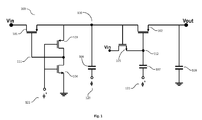
- Fig. 1 shows a circuit diagram of an example single stage charge pump voltage doubler 100.
- the voltage doubler 100 comprises a first PMOS (P-type metaloxide semiconductor) switch transistor 101 which is arranged to charge a boosting capacitor 106, when the control signal ⁇ 120 (also referred to as the capacitor control signal) driving the boosting capacitor 106 is low.
- the control signal ⁇ 120 takes on values between 0V (low level) and the input voltage Vin (high level).
- the first transistor 101 (also referred to as the first P-type switch) is configured to couple the input voltage Vin to the boosting capacitor 106, during a time interval, when the control signal ⁇ 120 is at low level.
- the first transistor 101 is configured to decouple the input voltage Vin from the boosting capacitor 106, during a time interval, when the control signal ⁇ 120 is at high level.
- a second PMOS switch transistor 102 is arranged to be off, in order to isolate the output voltage Vout from the node 110 connected to the boosting capacitor 106.
- This time interval may be referred to as the charging phase.
- the control signal ⁇ 120 which is driving the boosting capacitor 106 is at high level
- the node 110 connected to the boosting capacitor 106 has a voltage equal to two times the input voltage (i.e. 2 x Vin), in the idealized case.
- This time interval may be referred to as the discharging phase.
- the second transistor 102 (also referred to as the second P-type switch) may be arranged to be on, during the time interval, when the control signal ⁇ 120 is at high level, thereby transferring the increased voltage (i.e. 2 x Vin) to the output of the voltage doubler 100. During this phase, the first transistor 101 is turned off, thereby isolating the boosted voltage Vout from the input voltage Vin.
- the voltage doubler 100 comprises control or support circuitry for the first and the second transistors 101, 102.
- the support circuitry for the first transistor 101 comprises a high side switch 103 (e.g. a PMOS transistor) and a low side switch 104 (e.g. an NMOS transistor).
- the high side switch 103 and the low side switch 104 may be connected in a similar manner as an inverter block.
- the high side switch 103 and the low side switch 104 may be controlled using an inverted control signal ⁇ ' 121, wherein the inverted control signal ⁇ ' 121 is an inverted version of the control signal ⁇ 120.
- the low side switch 104 turns on and pulls down the gate voltage of the first transistor 101 to ground voltage.
- the first transistor 101 turns on (showing a relatively low resistance - 1/g ds between its drain and source nodes).
- the phase i.e. the charging phase
- the inverted control signal ⁇ ' 121 is at high level
- the node 110 connected to the boosting capacitor 106 has a voltage substantially equal to Vin and the high side switch 103 is off, thereby decoupling the gate node 111 of the first transistor 101 from the source node of the first transistor 101.
- the control signal ⁇ ' 121 driving the inverter i.e. driving the high side switch 103 and the low side switch 104
- the node 110 connected to the boosting capacitor 106 has a voltage equal to substantially 2xVin.
- the low side switch 104 is off, thereby decoupling the gate node 111 from ground.
- the high side switch 103 is on, thereby charging the gate voltage of the first transistor 101 to 2xVin, thus turning off the first transistor 101, and thereby decoupling the node 110 from the input voltage Vin.
- the support circuitry for the second transistor 102 comprises a control switch 105 (e.g. an NMOS transistor) and a control capacitor 107.
- the control capacitor 107 is coupled to the gate node 112 of the second transistor 102 (at a first side) and to the inverted control signal ⁇ ' 121 (at a second side).
- the control transistor 105 turns on, because during this phase, the gate of the control transistor 105 (which is coupled to the node 110) has a voltage equal to 2xVin.
- the drain of the control transistor 105 is coupled to the input voltage, and by consequence, the gate voltage of the second transistor (at node 112) is equal to the input voltage Vin, during the phase when the control signal ⁇ ' 121 is low.
- the source of the second transistor 102 has a voltage which is equal to 2xVin, and consequently, the second transistor 102 is turned on.
- the gate voltage of the second transistor 102 (at node 112) is boosted to a voltage equal to 2xVin.
- the source of the second transistor 102 has a voltage equal to the output voltage, i.e. two times the input voltage Vin, and the second transistor 102 is turned off.
- the control transistor 105 is off, because the gate of the control transistor (at node 110) has a voltage equal to the input Vin.
- the circuit 100 alternates charging phases and discharging phases and thereby transfers electrical energy from the input of the circuit 100 to the output of the circuit 100 using the boosting capacitor 106.
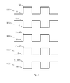
- Fig. 2 shows example control signals 120, 121 and example voltages at the nodes 110, 111, 112 of the voltage doubler 100 of Fig. 1 .
- the capacitor control signal 120 comprises alternating phases where the control signal 120 is at low level (e.g. 0V), referred to as the charging phases, and phases where the control signal 121 is at high level (e.g. Vin), referred to as the discharging phases.
- Typical commutation cycle rates are in the range of 1MHz, wherein a commutation cycle comprises one phase where the control signal 120 is at low level and one phase where the control signal 120 is at high level.
- the inverted control signal 121 is an inverted version of the control signal 120, such that the inverted control signal 121 is at low level, during a phase, when the control signal 120 is at high level, and vice versa.
- Fig. 2 also illustrates the voltage levels at the nodes 110, 111, 112 of the voltage doubler 100 of Fig. 1 , in response to the control signals 120, 121.
- the (high side) node 110 of the boosting capacitor 106 alternates between the input voltage Vin (during a phase for which the first transistor 101 is on (i.e. closed)) and 2 x Vin (during a phase for which the first transistor 101 is off (i.e. open)).
- the gate node 111 of the first transistor 101 alternates between 0V (in order to cause the first transistor 101 to be on (i.e. closed)) and 2 x Vin (in order to cause the first transistor 101 to be off).
- the gate node 112 of the second transistor 102 alternates between Vin (in order to cause the second transistor 102 to be off) and 2 x Vin (in order to cause the second transistor 102 to be on).
- the voltage doubler 100 of Fig. 1 is beneficial in that it makes use of only a single boosting capacitor 106 for transferring electrical energy from the input of the voltage doubler 100 to the output of the voltage doubler 100.
- an integrated circuit comprising the voltage doubler 100 only requires two pins for connecting the external boosting capacitor 106.
- the control capacitor 107 and the output capacitor 108 typically have a relatively low capacitance and can therefore be implemented as part of the integrated circuit (i.e. on-chip).
- the output capacitor 108 and the control capacitor 107 are not involved in the transfer of electrical energy from the input to the output of the voltage doubler 100.
- the voltage doubler 100 of Fig. 1 is beneficial, as it may be operable with relatively low input voltages Vin (e.g. in the range of 1V and smaller). This is due to the fact that the P-type transistors do not exhibit a significant body effect, which would reduce the voltage drop at the boosting capacitor 106 and the voltage drop at the output of the second transistor 102, and thereby reduce the level of the output voltage Vout that can be derived from the input voltage Vin. Furthermore the use of P-type transistors for the first and second transistors 101, 102 allows the power efficiency of the voltage doubler 100 to be increased. In addition, the voltage doubler 100 of Fig. 1 may be implemented using standard CMOS technology (without the need of using the more cost intensive triple well CMOS technology).
- NMOS transistors typically show a significant "body effect” when the source terminal voltages are greater than 0V.
- the "body effect” leads to an increase in threshold voltage, which leads to an increased switch resistance and to poor operations.
- PMOS transistors notably PMOS transistors with proper bulk connections, overcome this effect.
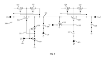
- Fig. 3 illustrates an implementation of the voltage doubler 100 using e.g. 0,35 ⁇ m CMOS technology without the triple well option.
- the voltage doubler 300 of Fig. 3 further comprises auxiliary transistors 311, 312 and 321, 322 for the first and second transistors 101, 102, respectively.
- the auxiliary transistors 311, 312, 321, 322 may be used to provide connections of the bulk of the PMOS parasitic diodes.
- the auxiliary transistors 311, 312, 321, 322 may be used to bypass the body diodes of the first and second transistors 101, 102, to further improve the performance of the voltage doubler 100, 300 and to allow for further decreased input voltages Vin.
- the auxiliary transistors 311, 312, 321, 322 may be used to couple the bulk of the first and second transistors 101, 102 to the source or to the drain of the first and second transistors 101, 102, respectively.
- Fig. 4 shows example performance results for the voltage doubler 300.
- the power efficiency 401 and the output voltage Vout 402 are plotted for a sweeping load current I LOAD 403 at the output of the voltage doubler 300.
- the clock signaling input source is as shown in Fig. 2 , i.e. no non-overlapping controls signals 120, 121 were used.
- the charge pump 100, 300 is operational without the need for a dedicated startup circuit.
- the output voltage (Vout) is typically only limited by the process breakdown voltages of the first and second transistors 101, 102.
- the described voltage doubler 100, 300 provides a power efficiency greater than 80%. Furthermore, the described voltage doubler 100, 300 provides output voltages Vout which are close to two times the input voltage Vin (e.g. greater than 1.9 times the input voltage Vin).
- Figs. 1 and 3 show a single stage voltage doubler, multiple stages of the voltage doublers 100, 300 may be cascaded, in order to provide further increased output voltages Vout.
- Fig. 5 shows a flow chart of an example method for generating an output voltage Vout at an output of the charge pump circuit (or voltage doubler) 100, 300 from an input voltage Vin at an input of the charge pump circuit 100, 300.
- the level of the output voltage Vout is typically greater than the level of the input voltage Vin.
- the input of the circuit 100, 300 may be coupled to a power supply which provides electrical power at the input voltage Vin.
- the method 500 comprises providing 501 a first P-type switch 101 (i.e. the first transistor 101) comprising an input node (i.e. the drain node) and an output node (i.e. the source node) 110.
- the input node of the first P-type switch 101 is coupled 502 to the input of the circuit 100, 300.
- the method comprises providing 503 a boosting capacitor 106 coupled at a first side to the output node 110 of the first P-type switch 101 and coupled at a second side to the capacitor control signal 120.
- a second P-type switch 102 i.e. the second transistor
- the method 500 also comprises coupling 505 the input node 110 of the second P-type switch 102 to the output node 110 of the first P-type switch 101, and coupling 506 the output node of the second P-type switch 102 to the output of the circuit 100, 300.
- the method 500 comprises providing 507 a capacitor control signal 120 which alternates between a low level and a high level.
- the method 500 also comprises generating 508 first and second control signals based on the capacitor control signal 120 for alternating the first and second P-type switches 101, 102 between on-states and off-states, respectively, such that electrical energy is transferred from the input to the output of the circuit 100, 300 using the boosting capacitor 106.
Landscapes
- Engineering & Computer Science (AREA)
- Power Engineering (AREA)
- Dc-Dc Converters (AREA)
Abstract
Description
- The present document relates to charge pump voltage doublers for use in integrated circuits. More particularly, the present document relates to charge pump voltage doublers with low input voltage, high efficiency and minimum off-chip components.
- Charge pump voltage doubler circuits are a building block of integrated circuits providing an output voltage higher than the power supply voltage. The trend for lower power supply voltages at the input of integrated circuits (e.g. in the context of single battery operation) and the trend for flexible operating conditions (e.g. in the context of wide input power supply range integrated circuits) are resulting in more applications for charge pump voltage doublers and creates the need for new design topologies performing with relatively low input voltages and with increased power efficiency.
- Charge pump voltage doublers may require two boosting capacitors per doubling stage. Furthermore, charge pump voltage doublers may only be operable for input voltages which are substantially higher than the threshold voltage of transistors comprised within the voltage doublers. In addition, charge pump voltage doublers may make use of triple well CMOS (Complementary metaloxide semiconductor) technology, thereby increasing the cost of the voltage doubler. Furthermore, charge pump voltage doublers may suffer from substantial power losses.
- The present document addresses the above mentioned technical problems. In particular, the present document describes a charge pump voltage doubler topology with high power efficiency, which uses only a single boosting capacitor per doubler stage and which may operate with relatively low input supply voltages. The charge pump voltage doubler which is described in the present document may be implemented using a standard CMOS process, without the need of using the relatively cost intensive triple well CMOS process.
- According to an aspect, a charge pump circuit (e.g. a voltage doubler circuit) configured to generate an output voltage Vout at an output of the charge pump circuit from an input voltage Vin at an input of the charge pump circuit is described. A level of the output voltage Vout may be greater than a level of the input voltage Vin. In particular, the level of the output voltage Vout may be approximately two times the input voltage Vin, e.g. 1.9 or more times the input voltage Vin. The input of the circuit may be coupled to a power supply providing electrical energy at the input voltage Vin to the charge pump circuit. The charge pump circuit may be implemented as an integrated circuit, using e.g. CMOS technology.
- The charge pump circuit comprises a first P-type switch comprising an input node (e.g. a drain) and an output node (e.g. a source). The P-type switch may comprise or may be a P-type metaloxide semiconductor (MOS) transistor. The input node of the first P-type switch is (directly) coupled to the input of the charge pump circuit. The use of a P-type switch is beneficial, as P-type switches typically exhibit no or reduced body effects, thereby allowing for the implementation of a charge pump circuit exhibiting an increased power efficiency.
- The charge pump circuit further comprises a boosting capacitor which is (directly) coupled at a first side to the output node (e.g. the source) of the first P-type switch and which is (directly) coupled at a second side to (or submitted to) a capacitor control signal. The boosting capacitor may be responsible for transferring electrical energy from the input to the output of the charge pump circuit. Furthermore, the boosting capacitor may be used to boost the output voltage with respect to the input voltage. The boosting capacitor may be external to an integrated circuit implementing the charge pump circuit. In such cases, the boosting capacitor may be coupled to the integrated circuit via a pair of pins of the integrated circuit.
- The charge pump circuit further comprises a second P-type switch comprising an input node (e.g. a drain) and an output node (e.g. a source). The P-type switch may comprise or may be a P-type metaloxide semiconductor (MOS) transistor. The input node of the second P-type switch is (directly) coupled to the output node of the first P-type switch, and the output node of the second P-type switch is (directly) coupled to the output of the charge pump circuit. As such, the first and second P-type switches may be used to couple the boosting capacitor with the input of the charge pump circuit and/or with the output of the charge pump circuit, respectively.
- In addition, the charge pump circuit comprises control circuitry configured to provide the capacitor control signal, wherein the capacitor control signal alternates between a low level and a high level. The capacitor control signal may alternate at a pre-determined commutation cycle rate or frequency, e.g. at 1MHz or more. The high level of the capacitor control signal may correspond to the level of the input voltage Vin. The low level of the capacitor control signal may correspond to a level which is lower than the level of the input voltage Vin (e.g. the level of ground). As such, the level of the boosting capacitor may be shifted between the low level and the high level, in order to provide an output voltage Vout which is increased compared to the input voltage Vin.
- The control circuitry is configured to generate first and second control signals based on the capacitor control signal for alternating the first and second P-type switches between on-states (when a switch is closed) and off-states (when a switch is open), respectively. The first and second control signals may be applied to gate nodes of the first and second P-type switches, respectively. The first and second control signals may be generated such that electrical energy is transferred from the input to the output of the circuit using the boosting capacitor. In particular, the first and second control signals may be generated such that the boosting capacitor is coupled to the input and the output of the charge pump circuit in a mutually exclusive manner and/or in an alternating manner. For this purpose, the first and second control signals may be generated to be in synchronicity with the capacitor control signal.
- As outlined above, the charge pump circuit makes use of P-type switches, thereby providing a power efficient charge pump circuit. Furthermore, the use of P-type switches enables relatively low input voltage Vin. In addition, the charge pump circuit makes use of only a single boosting capacitor for transferring the electrical energy from the input to the output of the charge pump circuit. By doing this, the number of pins (and consequently the costs) of the charge pump circuit can be reduced.
- The control circuitry may be configured to generate the first control signal, such that the first P-type switch is closed, when the capacitor control signal is at low level, to charge the boosting capacitor with electrical energy from the input of the circuit. This phase, when the boosting capacitor is coupled to the input of the charge pump circuit, may be referred to as a charging phase. Furthermore, the control circuitry may be configured to generate the first control signal, such that the first P-type switch is open, when the capacitor control signal is at high level. This phase, when the boosting capacitor is decoupled from the input of the charge pump circuit, may be referred to as a discharging phase.
- In other words, the first P-type switch may be closed to couple the boosting capacitor to the input voltage Vin, and to thereby bring the output node of the first P-type switch (i.e. the first side of the boosting capacitor) to the level of the input voltage Vin. Furthermore, the first P-type switch may be opened to decouple the boosting capacitor. By modifying the level of the second side of the boosting capacitor (using the capacitor control signal), the level of the first side of the boosting capacitor may be shifted. The electrical energy which is stored within the boosting capacitor may then be provided to the output of the charge pump circuit at the shifted voltage level.
- The control circuitry may comprise a high side switch and a low side switch, which are arranged in series between the output node of the first P-type switch and a reduced voltage level (e.g. ground). The high side and low side switches may be or may comprise MOS transistors. The high side switch may comprise a P-type switch, and/or the low side switch may comprise a N-type switch.
- A midpoint between the high side switch and the low side switch may be coupled to the gate node of the first P-type switch. The high side switch and the low side switch may be used to generate the first control signal. In particular, the high and low side switches may be configured to generate a first control signal which alternates between a high level and a low level. For this purpose, the high side switch may be configured to couple the output node of the first P-type switch with the gate node of the first P-type switch, when the high side switch is closed, to open the first P-type switch. Furthermore, the low side switch may be configured to couple the gate node of the first P-type switch to ground, when the low side switch is closed, to close the first P-type switch.
- The control circuitry may be configured to open and close the high side switch and the low side switch in a mutually exclusive manner, in order to open or close the first P-type switch. For this purpose, the gates nodes of the high side switch and of the low side switch may be coupled to an inverted version of the capacitor control signal, thereby controlling the first P-type switch in synchronicity with the capacitor control signal.
- The control circuitry may further be configured to generate the second control signal, such that the second P-type switch is closed, during the discharging phase, when the capacitor control signal is at high level, to discharge the boosting capacitor towards the output of the charge pump circuit. Furthermore, the second control signal may be generated such that the second P-type switch is open, during the charging phase, when the capacitor control signal is at low level.
- For this purpose, the control circuitry may comprise a control capacitor which is arranged between the gate node of the second P-type transistor (on a first side of the control transistor) and an inverted version of the capacitor control signal (which may be applied to a second side of the control transistor). As such, the control transistor may be used for boosting purposes, notably for boosting the voltage which is applied to the gate node of the second P-type transistor. However, the electrical energy which is taken up by the gate of the second P-type transistor is typically relatively small, such that the control transistor can be implemented on-chip.
- Furthermore, the control circuitry may comprise a control switch arranged between a power supply and the gate node of the second P-type transistor. The power supply may be configured to provide electrical energy at the input voltage Vin. The control switch may be or may comprise an N-type switch, e.g. an N-type MOS transistor. The control switch may be configured to couple the gate node of the second P-type transistor to the power supply for charging the control capacitor and for closing the second P-type switch. Furthermore, the control switch may be configured to decouple the gate node of the second P-type transistor from the power supply for opening the second P-type switch. For this purpose, a gate node of the control switch may be coupled to the output node of the first P-type switch.
- The charge pump circuit may comprise auxiliary switches (e.g. P-type MOS transistors) for bypassing parasitic diodes of the first and second P-type switches, respectively. By doing this, the power efficiency of the charge pump circuit may be further increased and/or the charge pump circuit may be used with further reduced input voltage Vin.
- The charge pump circuit may further comprise an output capacitor in parallel to the output of the circuit for reducing modulations of the output voltage Vout.
- According to another aspect, a method for generating an output voltage Vout at an output of a charge pump circuit from an input voltage Vin at an input of the charge pump circuit is described. A level of the output voltage Vout is typically greater than a level of the input voltage Vin. The input of the charge pump circuit may be coupled to a power supply which provides electrical power at the input voltage Vin. The method comprises providing a first P-type switch which comprises an input node and an output node. The input node of the first P-type switch may be coupled to the input of the charge pump circuit. Furthermore, the method comprises providing a boosting capacitor coupled at a first side to the output node of the first P-type switch and coupled at a second side to a capacitor control signal. In addition, a second P-type switch comprising an input node and an output node is provided. The method also comprises coupling the input node of the second P-type switch to the output node of the first P-type switch, and coupling the output node of the second P-type switch to the output of the charge pump circuit. In addition, the method comprises providing a capacitor control signal which alternates between a low level and a high level. The method also comprises generating first and second control signals based on the capacitor control signal for alternating the first and second P-type switches between on-states and off-states, respectively, such that electrical energy is transferred from the input to the output of the charge pump circuit using the boosting capacitor.
- It should be noted that the methods and systems including its preferred embodiments as outlined in the present document may be used stand-alone or in combination with the other methods and systems disclosed in this document. In addition, the features outlined in the context of a system are also applicable to a corresponding method. Furthermore, all aspects of the methods and systems outlined in the present document may be arbitrarily combined. In particular, the features of the claims may be combined with one another in an arbitrary manner.
- In the present document, the term "couple" or "coupled" refers to elements being in electrical communication with each other, whether directly connected e.g., via wires, or in some other manner.
- The invention is explained below in an exemplary manner with reference to the accompanying drawings, wherein
-
Fig. 1 illustrates a circuit diagram of an example single stage charge pump voltage doubler; -
Fig. 2 shows an example capacitor control signaling scheme and example node voltages describing the operation of the charge pump voltage doubler stage ofFig. 1 ; -
Fig. 3 shows a circuit diagram of an example single stage charge pump voltage doubler comprising additional bulk node connections; -
Fig. 4 shows example simulation results of the charge pump circuit ofFig. 3 ; and -
Fig. 5 shows a flow chart of an example method for increasing an input voltage. -
Fig. 1 shows a circuit diagram of an example single stage chargepump voltage doubler 100. Thevoltage doubler 100 comprises a first PMOS (P-type metaloxide semiconductor)switch transistor 101 which is arranged to charge a boostingcapacitor 106, when the control signal Φ 120 (also referred to as the capacitor control signal) driving the boostingcapacitor 106 is low. Typically, thecontrol signal Φ 120 takes on values between 0V (low level) and the input voltage Vin (high level). The first transistor 101 (also referred to as the first P-type switch) is configured to couple the input voltage Vin to the boostingcapacitor 106, during a time interval, when thecontrol signal Φ 120 is at low level. On the other hand, thefirst transistor 101 is configured to decouple the input voltage Vin from the boostingcapacitor 106, during a time interval, when thecontrol signal Φ 120 is at high level. - During the phase (or time interval), when the
control signal Φ 120 is at low level (and when the boostingcapacitor 106 is being charged), a secondPMOS switch transistor 102 is arranged to be off, in order to isolate the output voltage Vout from thenode 110 connected to the boostingcapacitor 106. This time interval may be referred to as the charging phase. When thecontrol signal Φ 120, which is driving the boostingcapacitor 106 is at high level, thenode 110 connected to the boostingcapacitor 106 has a voltage equal to two times the input voltage (i.e. 2 x Vin), in the idealized case. This time interval may be referred to as the discharging phase. The second transistor 102 (also referred to as the second P-type switch) may be arranged to be on, during the time interval, when thecontrol signal Φ 120 is at high level, thereby transferring the increased voltage (i.e. 2 x Vin) to the output of thevoltage doubler 100. During this phase, thefirst transistor 101 is turned off, thereby isolating the boosted voltage Vout from the input voltage Vin. - The
voltage doubler 100 comprises control or support circuitry for the first and thesecond transistors first transistor 101 comprises a high side switch 103 (e.g. a PMOS transistor) and a low side switch 104 (e.g. an NMOS transistor). Thehigh side switch 103 and thelow side switch 104 may be connected in a similar manner as an inverter block. Thehigh side switch 103 and thelow side switch 104 may be controlled using an inverted control signal Φ' 121, wherein the inverted control signal Φ' 121 is an inverted version of thecontrol signal Φ 120. When the control signal Φ' 121 driving thehigh side switch 103 and thelow side switch 104 is at high level (equal to Vin), thelow side switch 104 turns on and pulls down the gate voltage of thefirst transistor 101 to ground voltage. As a result of this, thefirst transistor 101 turns on (showing a relatively low resistance - 1/gds between its drain and source nodes). During the phase (i.e. the charging phase), when the inverted control signal Φ' 121 is at high level, thenode 110 connected to the boostingcapacitor 106 has a voltage substantially equal to Vin and thehigh side switch 103 is off, thereby decoupling thegate node 111 of thefirst transistor 101 from the source node of thefirst transistor 101. - In another phase (i.e. the discharging phase) the control signal Φ' 121 driving the inverter (i.e. driving the
high side switch 103 and the low side switch 104) is low (equal to 0V) and thenode 110 connected to the boostingcapacitor 106 has a voltage equal to substantially 2xVin. During this phase, thelow side switch 104 is off, thereby decoupling thegate node 111 from ground. At the same time, thehigh side switch 103 is on, thereby charging the gate voltage of thefirst transistor 101 to 2xVin, thus turning off thefirst transistor 101, and thereby decoupling thenode 110 from the input voltage Vin. - The support circuitry for the
second transistor 102 comprises a control switch 105 (e.g. an NMOS transistor) and acontrol capacitor 107. Thecontrol capacitor 107 is coupled to thegate node 112 of the second transistor 102 (at a first side) and to the inverted control signal Φ' 121 (at a second side). When the control signal Φ' 121 driving thecontrol capacitor 107 is low (equal to 0V), thecontrol transistor 105 turns on, because during this phase, the gate of the control transistor 105 (which is coupled to the node 110) has a voltage equal to 2xVin. In the illustrated example, the drain of thecontrol transistor 105 is coupled to the input voltage, and by consequence, the gate voltage of the second transistor (at node 112) is equal to the input voltage Vin, during the phase when the control signal Φ' 121 is low. During this phase (i.e. during the discharging phase), the source of thesecond transistor 102 has a voltage which is equal to 2xVin, and consequently, thesecond transistor 102 is turned on. - On the other hand, when the control signal Φ' 121 driving the
control capacitor 107 is high (equal to Vin), the gate voltage of the second transistor 102 (at node 112) is boosted to a voltage equal to 2xVin. During this phase (i.e. during the charging phase), the source of thesecond transistor 102 has a voltage equal to the output voltage, i.e. two times the input voltage Vin, and thesecond transistor 102 is turned off. Furthermore, during this phase thecontrol transistor 105 is off, because the gate of the control transistor (at node 110) has a voltage equal to the input Vin. - As such, the
circuit 100 alternates charging phases and discharging phases and thereby transfers electrical energy from the input of thecircuit 100 to the output of thecircuit 100 using the boostingcapacitor 106. -
Fig. 2 shows example control signals 120, 121 and example voltages at thenodes voltage doubler 100 ofFig. 1 . It can be seen that thecapacitor control signal 120 comprises alternating phases where thecontrol signal 120 is at low level (e.g. 0V), referred to as the charging phases, and phases where thecontrol signal 121 is at high level (e.g. Vin), referred to as the discharging phases. Typical commutation cycle rates are in the range of 1MHz, wherein a commutation cycle comprises one phase where thecontrol signal 120 is at low level and one phase where thecontrol signal 120 is at high level. As can be seen inFig. 2 , theinverted control signal 121 is an inverted version of thecontrol signal 120, such that theinverted control signal 121 is at low level, during a phase, when thecontrol signal 120 is at high level, and vice versa. -
Fig. 2 also illustrates the voltage levels at thenodes voltage doubler 100 ofFig. 1 , in response to the control signals 120, 121. As already outlined above, it can be seen that the (high side)node 110 of the boostingcapacitor 106 alternates between the input voltage Vin (during a phase for which thefirst transistor 101 is on (i.e. closed)) and 2 x Vin (during a phase for which thefirst transistor 101 is off (i.e. open)). Thegate node 111 of thefirst transistor 101 alternates between 0V (in order to cause thefirst transistor 101 to be on (i.e. closed)) and 2 x Vin (in order to cause thefirst transistor 101 to be off). Thegate node 112 of thesecond transistor 102 alternates between Vin (in order to cause thesecond transistor 102 to be off) and 2 x Vin (in order to cause thesecond transistor 102 to be on). - The
voltage doubler 100 ofFig. 1 is beneficial in that it makes use of only a single boostingcapacitor 106 for transferring electrical energy from the input of thevoltage doubler 100 to the output of thevoltage doubler 100. Hence, an integrated circuit comprising thevoltage doubler 100 only requires two pins for connecting the external boostingcapacitor 106. It should be noted that thecontrol capacitor 107 and theoutput capacitor 108 typically have a relatively low capacitance and can therefore be implemented as part of the integrated circuit (i.e. on-chip). In contrast to the boostingcapacitor 106, theoutput capacitor 108 and thecontrol capacitor 107 are not involved in the transfer of electrical energy from the input to the output of thevoltage doubler 100. - Furthermore, the
voltage doubler 100 ofFig. 1 is beneficial, as it may be operable with relatively low input voltages Vin (e.g. in the range of 1V and smaller). This is due to the fact that the P-type transistors do not exhibit a significant body effect, which would reduce the voltage drop at the boostingcapacitor 106 and the voltage drop at the output of thesecond transistor 102, and thereby reduce the level of the output voltage Vout that can be derived from the input voltage Vin. Furthermore the use of P-type transistors for the first andsecond transistors voltage doubler 100 to be increased. In addition, thevoltage doubler 100 ofFig. 1 may be implemented using standard CMOS technology (without the need of using the more cost intensive triple well CMOS technology). - The above mentioned benefits are due to the use of P-type transistors. In contrast to this, NMOS transistors typically show a significant "body effect" when the source terminal voltages are greater than 0V. The "body effect" leads to an increase in threshold voltage, which leads to an increased switch resistance and to poor operations. PMOS transistors, notably PMOS transistors with proper bulk connections, overcome this effect.
-
Fig. 3 illustrates an implementation of thevoltage doubler 100 using e.g. 0,35µm CMOS technology without the triple well option. Thevoltage doubler 300 ofFig. 3 further comprisesauxiliary transistors second transistors auxiliary transistors auxiliary transistors second transistors voltage doubler auxiliary transistors second transistors second transistors -
Fig. 4 shows example performance results for thevoltage doubler 300. In particular,Fig. 4 gives simulation results for an input voltage Vin=1V. Thepower efficiency 401 and theoutput voltage Vout 402 are plotted for a sweeping load current ILOAD 403 at the output of thevoltage doubler 300. For the simulations, the clock signaling input source is as shown inFig. 2 , i.e. no non-overlapping controls signals 120, 121 were used. However, it has been observed that the describedvoltage doubler charge pump second transistors - As can be seen from
Fig. 4 , the describedvoltage doubler voltage doubler - It should be noted that while
Figs. 1 and3 show a single stage voltage doubler, multiple stages of thevoltage doublers -
Fig. 5 shows a flow chart of an example method for generating an output voltage Vout at an output of the charge pump circuit (or voltage doubler) 100, 300 from an input voltage Vin at an input of thecharge pump circuit circuit method 500 comprises providing 501 a first P-type switch 101 (i.e. the first transistor 101) comprising an input node (i.e. the drain node) and an output node (i.e. the source node) 110. The input node of the first P-type switch 101 is coupled 502 to the input of thecircuit capacitor 106 coupled at a first side to theoutput node 110 of the first P-type switch 101 and coupled at a second side to thecapacitor control signal 120. In addition, a second P-type switch 102 (i.e. the second transistor) comprising an input node (i.e. the drain node) 110 and an output node (i.e. the source node) is provided 504. Themethod 500 also comprises coupling 505 theinput node 110 of the second P-type switch 102 to theoutput node 110 of the first P-type switch 101, andcoupling 506 the output node of the second P-type switch 102 to the output of thecircuit method 500 comprises providing 507 acapacitor control signal 120 which alternates between a low level and a high level. Themethod 500 also comprises generating 508 first and second control signals based on thecapacitor control signal 120 for alternating the first and second P-type switches circuit capacitor 106. - It should be noted that the description and drawings merely illustrate the principles of the proposed methods and systems. Those skilled in the art will be able to implement various arrangements that, although not explicitly described or shown herein, embody the principles of the invention and are included within its spirit and scope. Furthermore, all examples and embodiment outlined in the present document are principally intended expressly to be only for explanatory purposes to help the reader in understanding the principles of the proposed methods and systems. Furthermore, all statements herein providing principles, aspects, and embodiments of the invention, as well as specific examples thereof, are intended to encompass equivalents thereof.
Claims (15)
- A charge pump circuit (100, 300) configured to generate an output voltage Vout at an output of the circuit (100, 300) from an input voltage Vin at an input of the circuit (100, 300), wherein a level of the output voltage Vout is greater than a level of the input voltage Vin; wherein the charge pump circuit (100, 300) comprises- a first P-type switch (101) comprising an input node and an output node (110); wherein the input node of the first P-type switch (101) is coupled to the input of the circuit (100, 300);- a boosting capacitor (106) coupled at a first side to the output node (110) of the first P-type switch (101) and coupled at a second side to a capacitor control signal (120);- a second P-type switch (102) comprising an input node (110) and an output node; wherein the input node (110) of the second P-type switch (102) is coupled to the output node (110) of the first P-type switch (101), and wherein the output node of the second P-type switch (102) is coupled to the output of the circuit (100, 300); and- control circuitry (103, 104, 105, 107) configured to provide a capacitor control signal (120) which alternates between a low level and a high level, and configured to generate first and second control signals based on the capacitor control signal (120) for alternating the first and second P-type switches (101, 102) between on-states and off-states, respectively, such that electrical energy is transferred from the input to the output of the circuit (100, 300) using the boosting capacitor (106).
- The charge pump circuit (100, 300) of claim 1, wherein the first and second control signals are in synchronicity with the capacitor control signal (120).
- The charge pump circuit (100, 300) of any previous claim, wherein the first and second control signals are applied to gate nodes (111, 112) of the first and second P-type switches (101, 102), respectively.
- The charge pump circuit (100, 300) of any previous claim, wherein- the high level of the capacitor control signal (120) corresponds to the level of the input voltage Vin; and- the low level of the capacitor control signal (120) corresponds to the level of ground.
- The charge pump circuit (100, 300) of any previous claim, wherein the control circuitry (103, 104, 105, 107) is configured to generate the first control signal, such that- the first P-type switch (101) is closed, during a charging phase, when the capacitor control signal (120) is at low level, to charge the boosting capacitor (106) from the input of the circuit (100, 300); and/or- the first P-type switch (101) is open, during a discharging phase, when the capacitor control signal (120) is at high level.
- The charge pump circuit (100, 300) of claim 5, wherein the control circuitry (103, 104, 105, 107) comprises- a high side switch (103) and a low side switch (104) which are arranged in series between the output node (110) of the first P-type switch (101) and ground; and- a midpoint between the high side switch (103) and the low side switch (104) is coupled to a gate node (111) of the first P-type switch (101); wherein the high side switch (103) is configured to couple the output node (110) with the gate node (111) of the first P-type switch (101), when the high side switch (103) is closed, to open the first P-type switch (101); and wherein the low side switch (104) is configured to couple the gate node (111) of the first P-type switch (101) to ground, when the low side switch (103) is closed, to close the first P-type switch (101).
- The charge pump circuit (100, 300) of claim 5, wherein the control circuitry (103, 104, 105, 107) is configured to open and close the high side switch (103) and the low side switch (104) in a mutually exclusive manner.
- The charge pump circuit (100, 300) of any of claims 5 to 6, wherein- the high side switch (103) comprises a P-type switch;- the low side switch (104) comprises a N-type switch; and- gates nodes of the high side switch (103) and of the low side switch (104) are coupled to an inverted version (121) of the capacitor control signal (120).
- The charge pump circuit (100, 300) of any previous claim, wherein the control circuitry (103, 104, 105, 107) is configured to generate the second control signal, such that- the second P-type switch (102) is closed, during a discharging phase, when the capacitor control signal (120) is at high level, to discharge the boosting capacitor (106) towards the output of the circuit (100, 300); and/or- the second P-type switch (102) is open, during a charging phase, when the capacitor control signal (120) is at low level.
- The charge pump circuit (100, 300) of claim 9, wherein the control circuitry (103, 104, 105, 107) comprises- a control capacitor (107) arranged between a gate node (112) of the second P-type transistor and an inverted version (121) of the capacitor control signal (120); and- a control switch (105) arranged between a power supply and the gate node (112) of the second P-type transistor; wherein the control switch (105) is configured to couple the gate node (112) to the power supply for charging the control capacitor (107) and for closing the second P-type switch (102); and wherein the control switch (105) is configured to decouple the gate node (112) from the power supply for opening the second P-type switch (102).
- The charge pump circuit (100, 300) of claim 10, wherein- the control switch (105) comprises an N-type switch; and- a gate node of the control switch (105) is coupled to the output node (110) of the first P-type switch (101).
- The charge pump circuit (100, 300) of any previous claim, wherein the first and second P-type switches (101, 102) are P-type metaloxide semiconductor transistors.
- The charge pump circuit (100, 300) of any previous claim, further comprising auxiliary switches (311, 312, 321, 322) for bypassing parasitic diodes of the first and second P-type switches, respectively.
- The charge pump circuit (100, 300) of any previous claim, further comprising an output capacitor (108) in parallel to the output of the circuit (100, 300).
- A method (500) for generating an output voltage Vout at an output of a charge pump circuit (100, 300) from an input voltage Vin at an input of the charge pump circuit (100, 300), wherein a level of the output voltage Vout is greater than a level of the input voltage Vin; wherein the method (500) comprises- providing (501) a first P-type switch (101) comprising an input node and an output node (110);- coupling (502) the input node of the first P-type switch (101) to the input of the circuit (100, 300);- providing (503) a boosting capacitor (106) coupled at a first side to the output node (110) of the first P-type switch (101) and coupled at a second side to a capacitor control signal (120);- providing (504) a second P-type switch (102) comprising an input node (110) and an output node;- coupling (505) the input node (110) of the second P-type switch (102) to the output node (110) of the first P-type switch (101);- coupling (506) the output node of the second P-type switch (102) to the output of the circuit (100, 300);- providing (507) a capacitor control signal (120) which alternates between a low level and a high level; and- generating (508) first and second control signals based on the capacitor control signal (120) for alternating the first and second P-type switches (101, 102) between on-states and off-states, respectively, such that electrical energy is transferred from the input to the output of the circuit (100, 300) using the boosting capacitor (106).
Priority Applications (2)
| Application Number | Priority Date | Filing Date | Title |
|---|---|---|---|
| EP20130188374 EP2860865A1 (en) | 2013-10-11 | 2013-10-11 | High efficiency charge pump circuit |
| US14/316,926 US9112406B2 (en) | 2013-10-11 | 2014-06-27 | High efficiency charge pump circuit |
Applications Claiming Priority (1)
| Application Number | Priority Date | Filing Date | Title |
|---|---|---|---|
| EP20130188374 EP2860865A1 (en) | 2013-10-11 | 2013-10-11 | High efficiency charge pump circuit |
Publications (1)
| Publication Number | Publication Date |
|---|---|
| EP2860865A1 true EP2860865A1 (en) | 2015-04-15 |
Family
ID=49354517
Family Applications (1)
| Application Number | Title | Priority Date | Filing Date |
|---|---|---|---|
| EP20130188374 Withdrawn EP2860865A1 (en) | 2013-10-11 | 2013-10-11 | High efficiency charge pump circuit |
Country Status (2)
| Country | Link |
|---|---|
| US (1) | US9112406B2 (en) |
| EP (1) | EP2860865A1 (en) |
Families Citing this family (1)
| Publication number | Priority date | Publication date | Assignee | Title |
|---|---|---|---|---|
| CN109994141A (en) * | 2017-12-31 | 2019-07-09 | 北京同方微电子有限公司 | A Shared Charge Pump System Applied to Flash Structure Memory |
Citations (7)
| Publication number | Priority date | Publication date | Assignee | Title |
|---|---|---|---|---|
| US5587683A (en) * | 1993-12-09 | 1996-12-24 | Kabushiki Kaisha Toshiba | Booster circuit device |
| JP2001136733A (en) * | 1999-11-01 | 2001-05-18 | Seiko Epson Corp | Charge pump circuit |
| US20050206441A1 (en) * | 2004-03-19 | 2005-09-22 | Semiconductor Energy Laboratory Co., Ltd. | Booster circuit, semiconductor device, and electronic apparatus |
| US20070075765A1 (en) * | 2005-09-30 | 2007-04-05 | Nec Electronics Corporation | Booster circuit |
| US20090167419A1 (en) * | 2007-12-28 | 2009-07-02 | Nec Electronics Corporation | Voltage converting circuit |
| US20090201280A1 (en) * | 2008-01-31 | 2009-08-13 | Tpo Displays Corp. | Image display system |
| CN102446480A (en) * | 2010-10-14 | 2012-05-09 | 上海天马微电子有限公司 | Voltage conversion circuit |
Family Cites Families (17)
| Publication number | Priority date | Publication date | Assignee | Title |
|---|---|---|---|---|
| DE19627197C1 (en) | 1996-07-05 | 1998-03-26 | Siemens Ag | Device for voltage multiplication with little dependence of the output voltage on the supply voltage |
| JP3488587B2 (en) * | 1997-01-09 | 2004-01-19 | 株式会社東芝 | Boost circuit and IC card having the same |
| US6078212A (en) * | 1997-08-18 | 2000-06-20 | Micron Technology, Inc. | VT cancellation in output stage of charge pump |
| US6191642B1 (en) * | 1999-03-30 | 2001-02-20 | Silicon Storage Technology, Inc. | Charge pump circuit |
| DE19953882C2 (en) * | 1999-11-09 | 2001-10-18 | Infineon Technologies Ag | Charge pump for generating high voltages for semiconductor circuits |
| JP3702166B2 (en) * | 2000-02-04 | 2005-10-05 | 三洋電機株式会社 | Charge pump circuit |
| US6661682B2 (en) | 2001-02-16 | 2003-12-09 | Imec (Interuniversitair Microelectronica Centrum) | High voltage generating charge pump circuit |
| JP4336489B2 (en) * | 2002-11-18 | 2009-09-30 | 株式会社ルネサステクノロジ | Semiconductor integrated circuit |
| TW583818B (en) | 2002-12-03 | 2004-04-11 | Via Tech Inc | Charge pump and voltage doubler using the same |
| TW200505162A (en) * | 2003-04-14 | 2005-02-01 | Sanyo Electric Co | Charge pump circuit |
| KR100510552B1 (en) * | 2003-10-27 | 2005-08-26 | 삼성전자주식회사 | Charge pump circuit having improved charge transfer effiency |
| FR2864271B1 (en) | 2003-12-19 | 2006-03-03 | Atmel Corp | HIGH EFFICIENCY, LOW COST LOAD PUMP CIRCUIT |
| KR100573780B1 (en) | 2004-05-25 | 2006-04-25 | 재단법인서울대학교산학협력재단 | Charge pump |
| US8120413B2 (en) * | 2008-08-18 | 2012-02-21 | Semiconductor Manufacturing International (Beijing) Corporation | Charge pump circuit |
| JP5342324B2 (en) * | 2009-05-26 | 2013-11-13 | ルネサスエレクトロニクス株式会社 | Booster circuit |
| US9059630B2 (en) * | 2011-08-31 | 2015-06-16 | Knowles Electronics, Llc | High voltage multiplier for a microphone and method of manufacture |
| KR20130093303A (en) * | 2012-02-14 | 2013-08-22 | 에스케이하이닉스 주식회사 | Charge pumping device and unit cell thereof |
-
2013
- 2013-10-11 EP EP20130188374 patent/EP2860865A1/en not_active Withdrawn
-
2014
- 2014-06-27 US US14/316,926 patent/US9112406B2/en active Active
Patent Citations (7)
| Publication number | Priority date | Publication date | Assignee | Title |
|---|---|---|---|---|
| US5587683A (en) * | 1993-12-09 | 1996-12-24 | Kabushiki Kaisha Toshiba | Booster circuit device |
| JP2001136733A (en) * | 1999-11-01 | 2001-05-18 | Seiko Epson Corp | Charge pump circuit |
| US20050206441A1 (en) * | 2004-03-19 | 2005-09-22 | Semiconductor Energy Laboratory Co., Ltd. | Booster circuit, semiconductor device, and electronic apparatus |
| US20070075765A1 (en) * | 2005-09-30 | 2007-04-05 | Nec Electronics Corporation | Booster circuit |
| US20090167419A1 (en) * | 2007-12-28 | 2009-07-02 | Nec Electronics Corporation | Voltage converting circuit |
| US20090201280A1 (en) * | 2008-01-31 | 2009-08-13 | Tpo Displays Corp. | Image display system |
| CN102446480A (en) * | 2010-10-14 | 2012-05-09 | 上海天马微电子有限公司 | Voltage conversion circuit |
Also Published As
| Publication number | Publication date |
|---|---|
| US9112406B2 (en) | 2015-08-18 |
| US20150102854A1 (en) | 2015-04-16 |
Similar Documents
| Publication | Publication Date | Title |
|---|---|---|
| US11901818B1 (en) | Power supply for gate driver in switched-capacitor circuit | |
| KR101375017B1 (en) | Voltage up-conversion circuit using low voltage transistors | |
| US9806616B2 (en) | Control circuit for multiple high side switches | |
| TW201813263A (en) | Balancing techniques and circuits for charge pumps | |
| US9634562B1 (en) | Voltage doubling circuit and charge pump applications for the voltage doubling circuit | |
| CN207200574U (en) | Circuit structure | |
| US10476383B2 (en) | Negative charge pump circuit | |
| US9923459B2 (en) | Charge pump | |
| US20190372458A1 (en) | Elementary cell and charge pumps comprising such an elementary cell | |
| TWI439840B (en) | Charge pump | |
| CN110912401B (en) | Voltage multiplying circuit | |
| US20090309650A1 (en) | Booster circuit | |
| US7683699B2 (en) | Charge pump | |
| CN104124951B (en) | Circuit for driving high-side transistor | |
| US20160164404A1 (en) | Cold start dc/dc converter | |
| US9112406B2 (en) | High efficiency charge pump circuit | |
| TWI703802B (en) | Cross-coupled charge pumps and methods of operating same | |
| CN107395012A (en) | A kind of charge pump circuit and its control method | |
| CN113014240B (en) | Control circuit of signal switch tube and analog switch circuit | |
| Wong et al. | A low-voltage charge pump with wide current driving capability | |
| Yu et al. | Half-bridge driver with charge pump based high-side voltage regulator | |
| CN106444943A (en) | Voltage generating circuit | |
| CN121283186A (en) | Charge pump apparatus | |
| JP2011166916A (en) | Voltage conversion circuit, and voltage conversion method |
Legal Events
| Date | Code | Title | Description |
|---|---|---|---|
| PUAI | Public reference made under article 153(3) epc to a published international application that has entered the european phase |
Free format text: ORIGINAL CODE: 0009012 |
|
| 17P | Request for examination filed |
Effective date: 20131011 |
|
| AK | Designated contracting states |
Kind code of ref document: A1 Designated state(s): AL AT BE BG CH CY CZ DE DK EE ES FI FR GB GR HR HU IE IS IT LI LT LU LV MC MK MT NL NO PL PT RO RS SE SI SK SM TR |
|
| AX | Request for extension of the european patent |
Extension state: BA ME |
|
| R17P | Request for examination filed (corrected) |
Effective date: 20150402 |
|
| RBV | Designated contracting states (corrected) |
Designated state(s): AL AT BE BG CH CY CZ DE DK EE ES FI FR GB GR HR HU IE IS IT LI LT LU LV MC MK MT NL NO PL PT RO RS SE SI SK SM TR |
|
| STAA | Information on the status of an ep patent application or granted ep patent |
Free format text: STATUS: EXAMINATION IS IN PROGRESS |
|
| 17Q | First examination report despatched |
Effective date: 20161207 |
|
| STAA | Information on the status of an ep patent application or granted ep patent |
Free format text: STATUS: THE APPLICATION IS DEEMED TO BE WITHDRAWN |
|
| 18D | Application deemed to be withdrawn |
Effective date: 20190501 |