EP2860773A1 - Light-emitting device, light-emitting device package, and light unit - Google Patents
Light-emitting device, light-emitting device package, and light unit Download PDFInfo
- Publication number
- EP2860773A1 EP2860773A1 EP13800692.9A EP13800692A EP2860773A1 EP 2860773 A1 EP2860773 A1 EP 2860773A1 EP 13800692 A EP13800692 A EP 13800692A EP 2860773 A1 EP2860773 A1 EP 2860773A1
- Authority
- EP
- European Patent Office
- Prior art keywords
- light
- layer
- semiconductor layer
- emitting device
- conductive semiconductor
- Prior art date
- Legal status (The legal status is an assumption and is not a legal conclusion. Google has not performed a legal analysis and makes no representation as to the accuracy of the status listed.)
- Granted
Links
Images




Classifications
-
- H—ELECTRICITY
- H10—SEMICONDUCTOR DEVICES; ELECTRIC SOLID-STATE DEVICES NOT OTHERWISE PROVIDED FOR
- H10H—INORGANIC LIGHT-EMITTING SEMICONDUCTOR DEVICES HAVING POTENTIAL BARRIERS
- H10H20/00—Individual inorganic light-emitting semiconductor devices having potential barriers, e.g. light-emitting diodes [LED]
- H10H20/80—Constructional details
- H10H20/81—Bodies
- H10H20/814—Bodies having reflecting means, e.g. semiconductor Bragg reflectors
-
- H—ELECTRICITY
- H10—SEMICONDUCTOR DEVICES; ELECTRIC SOLID-STATE DEVICES NOT OTHERWISE PROVIDED FOR
- H10H—INORGANIC LIGHT-EMITTING SEMICONDUCTOR DEVICES HAVING POTENTIAL BARRIERS
- H10H20/00—Individual inorganic light-emitting semiconductor devices having potential barriers, e.g. light-emitting diodes [LED]
- H10H20/80—Constructional details
- H10H20/83—Electrodes
-
- H—ELECTRICITY
- H10—SEMICONDUCTOR DEVICES; ELECTRIC SOLID-STATE DEVICES NOT OTHERWISE PROVIDED FOR
- H10H—INORGANIC LIGHT-EMITTING SEMICONDUCTOR DEVICES HAVING POTENTIAL BARRIERS
- H10H20/00—Individual inorganic light-emitting semiconductor devices having potential barriers, e.g. light-emitting diodes [LED]
- H10H20/80—Constructional details
- H10H20/84—Coatings, e.g. passivation layers or antireflective coatings
- H10H20/841—Reflective coatings, e.g. dielectric Bragg reflectors
-
- H—ELECTRICITY
- H10—SEMICONDUCTOR DEVICES; ELECTRIC SOLID-STATE DEVICES NOT OTHERWISE PROVIDED FOR
- H10H—INORGANIC LIGHT-EMITTING SEMICONDUCTOR DEVICES HAVING POTENTIAL BARRIERS
- H10H20/00—Individual inorganic light-emitting semiconductor devices having potential barriers, e.g. light-emitting diodes [LED]
- H10H20/80—Constructional details
- H10H20/85—Packages
-
- F—MECHANICAL ENGINEERING; LIGHTING; HEATING; WEAPONS; BLASTING
- F21—LIGHTING
- F21K—NON-ELECTRIC LIGHT SOURCES USING LUMINESCENCE; LIGHT SOURCES USING ELECTROCHEMILUMINESCENCE; LIGHT SOURCES USING CHARGES OF COMBUSTIBLE MATERIAL; LIGHT SOURCES USING SEMICONDUCTOR DEVICES AS LIGHT-GENERATING ELEMENTS; LIGHT SOURCES NOT OTHERWISE PROVIDED FOR
- F21K9/00—Light sources using semiconductor devices as light-generating elements, e.g. using light-emitting diodes [LED] or lasers
- F21K9/20—Light sources comprising attachment means
- F21K9/23—Retrofit light sources for lighting devices with a single fitting for each light source, e.g. for substitution of incandescent lamps with bayonet or threaded fittings
- F21K9/232—Retrofit light sources for lighting devices with a single fitting for each light source, e.g. for substitution of incandescent lamps with bayonet or threaded fittings specially adapted for generating an essentially omnidirectional light distribution, e.g. with a glass bulb
-
- F—MECHANICAL ENGINEERING; LIGHTING; HEATING; WEAPONS; BLASTING
- F21—LIGHTING
- F21V—FUNCTIONAL FEATURES OR DETAILS OF LIGHTING DEVICES OR SYSTEMS THEREOF; STRUCTURAL COMBINATIONS OF LIGHTING DEVICES WITH OTHER ARTICLES, NOT OTHERWISE PROVIDED FOR
- F21V29/00—Protecting lighting devices from thermal damage; Cooling or heating arrangements specially adapted for lighting devices or systems
- F21V29/50—Cooling arrangements
- F21V29/70—Cooling arrangements characterised by passive heat-dissipating elements, e.g. heat-sinks
- F21V29/74—Cooling arrangements characterised by passive heat-dissipating elements, e.g. heat-sinks with fins or blades
-
- F—MECHANICAL ENGINEERING; LIGHTING; HEATING; WEAPONS; BLASTING
- F21—LIGHTING
- F21V—FUNCTIONAL FEATURES OR DETAILS OF LIGHTING DEVICES OR SYSTEMS THEREOF; STRUCTURAL COMBINATIONS OF LIGHTING DEVICES WITH OTHER ARTICLES, NOT OTHERWISE PROVIDED FOR
- F21V3/00—Globes; Bowls; Cover glasses
- F21V3/04—Globes; Bowls; Cover glasses characterised by materials, surface treatments or coatings
- F21V3/06—Globes; Bowls; Cover glasses characterised by materials, surface treatments or coatings characterised by the material
- F21V3/061—Globes; Bowls; Cover glasses characterised by materials, surface treatments or coatings characterised by the material the material being glass
-
- F—MECHANICAL ENGINEERING; LIGHTING; HEATING; WEAPONS; BLASTING
- F21—LIGHTING
- F21V—FUNCTIONAL FEATURES OR DETAILS OF LIGHTING DEVICES OR SYSTEMS THEREOF; STRUCTURAL COMBINATIONS OF LIGHTING DEVICES WITH OTHER ARTICLES, NOT OTHERWISE PROVIDED FOR
- F21V3/00—Globes; Bowls; Cover glasses
- F21V3/04—Globes; Bowls; Cover glasses characterised by materials, surface treatments or coatings
- F21V3/06—Globes; Bowls; Cover glasses characterised by materials, surface treatments or coatings characterised by the material
- F21V3/062—Globes; Bowls; Cover glasses characterised by materials, surface treatments or coatings characterised by the material the material being plastics
-
- F—MECHANICAL ENGINEERING; LIGHTING; HEATING; WEAPONS; BLASTING
- F21—LIGHTING
- F21Y—INDEXING SCHEME ASSOCIATED WITH SUBCLASSES F21K, F21L, F21S and F21V, RELATING TO THE FORM OR THE KIND OF THE LIGHT SOURCES OR OF THE COLOUR OF THE LIGHT EMITTED
- F21Y2107/00—Light sources with three-dimensionally disposed light-generating elements
- F21Y2107/30—Light sources with three-dimensionally disposed light-generating elements on the outer surface of cylindrical surfaces, e.g. rod-shaped supports having a circular or a polygonal cross section
-
- F—MECHANICAL ENGINEERING; LIGHTING; HEATING; WEAPONS; BLASTING
- F21—LIGHTING
- F21Y—INDEXING SCHEME ASSOCIATED WITH SUBCLASSES F21K, F21L, F21S and F21V, RELATING TO THE FORM OR THE KIND OF THE LIGHT SOURCES OR OF THE COLOUR OF THE LIGHT EMITTED
- F21Y2113/00—Combination of light sources
-
- F—MECHANICAL ENGINEERING; LIGHTING; HEATING; WEAPONS; BLASTING
- F21—LIGHTING
- F21Y—INDEXING SCHEME ASSOCIATED WITH SUBCLASSES F21K, F21L, F21S and F21V, RELATING TO THE FORM OR THE KIND OF THE LIGHT SOURCES OR OF THE COLOUR OF THE LIGHT EMITTED
- F21Y2115/00—Light-generating elements of semiconductor light sources
- F21Y2115/10—Light-emitting diodes [LED]
-
- H—ELECTRICITY
- H10—SEMICONDUCTOR DEVICES; ELECTRIC SOLID-STATE DEVICES NOT OTHERWISE PROVIDED FOR
- H10H—INORGANIC LIGHT-EMITTING SEMICONDUCTOR DEVICES HAVING POTENTIAL BARRIERS
- H10H20/00—Individual inorganic light-emitting semiconductor devices having potential barriers, e.g. light-emitting diodes [LED]
- H10H20/01—Manufacture or treatment
- H10H20/011—Manufacture or treatment of bodies, e.g. forming semiconductor layers
- H10H20/018—Bonding of wafers
-
- H—ELECTRICITY
- H10—SEMICONDUCTOR DEVICES; ELECTRIC SOLID-STATE DEVICES NOT OTHERWISE PROVIDED FOR
- H10H—INORGANIC LIGHT-EMITTING SEMICONDUCTOR DEVICES HAVING POTENTIAL BARRIERS
- H10H20/00—Individual inorganic light-emitting semiconductor devices having potential barriers, e.g. light-emitting diodes [LED]
- H10H20/80—Constructional details
- H10H20/81—Bodies
- H10H20/819—Bodies characterised by their shape, e.g. curved or truncated substrates
- H10H20/82—Roughened surfaces, e.g. at the interface between epitaxial layers
-
- H—ELECTRICITY
- H10—SEMICONDUCTOR DEVICES; ELECTRIC SOLID-STATE DEVICES NOT OTHERWISE PROVIDED FOR
- H10W—GENERIC PACKAGES, INTERCONNECTIONS, CONNECTORS OR OTHER CONSTRUCTIONAL DETAILS OF DEVICES COVERED BY CLASS H10
- H10W74/00—Encapsulations, e.g. protective coatings
-
- H—ELECTRICITY
- H10—SEMICONDUCTOR DEVICES; ELECTRIC SOLID-STATE DEVICES NOT OTHERWISE PROVIDED FOR
- H10W—GENERIC PACKAGES, INTERCONNECTIONS, CONNECTORS OR OTHER CONSTRUCTIONAL DETAILS OF DEVICES COVERED BY CLASS H10
- H10W90/00—Package configurations
- H10W90/701—Package configurations characterised by the relative positions of pads or connectors relative to package parts
- H10W90/751—Package configurations characterised by the relative positions of pads or connectors relative to package parts of bond wires
- H10W90/756—Package configurations characterised by the relative positions of pads or connectors relative to package parts of bond wires between a chip and a stacked lead frame, conducting package substrate or heat sink
Definitions
- the embodiment relates to a light-emitting device, a light-emitting device package, and a light unit.
- a light-emitting diode has been extensively used as one of light-emitting devices.
- the LED converts electrical signals into the form of light such as infra-red light, ultra-violet light, and visible light by using the characteristic of a compound semiconductor.
- the LED As the light efficiency of the light-emitting device is increased, the LED has been used in various fields such as display apparatuses and lighting appliances.
- the embodiment provides a light-emitting device, a light-emitting device package, and a light unit, capable of improving light extraction efficiency.
- a light-emitting device includes a light-emitting structure including a first conductive semiconductor layer, an active layer under the first conductive semiconductor layer, and a second conductive semiconductor layer under the active layer; a first electrode arranged under the light-emitting structure and electrically connected to the second conductive semiconductor layer; a reflective layer arranged inside the second conductive semiconductor layer and spaced apart from the first electrode and the active layer; and a second electrode electrically connected to the first conductive semiconductor layer.
- a light-emitting device package includes a body; a light-emitting device on the body; and first and second lead electrodes electrically connected to the light-emitting device, wherein the light-emitting device includes a light-emitting structure including a first conductive semiconductor layer, an active layer under the first conductive semiconductor layer, and a second conductive semiconductor layer under the active layer; a first electrode arranged under the light-emitting structure and electrically connected to the second conductive semiconductor layer; a reflective layer arranged inside the second conductive semiconductor layer and spaced apart from the first electrode and the active layer; and a second electrode electrically connected to the first conductive semiconductor layer.
- the light-emitting device includes a light-emitting structure including a first conductive semiconductor layer, an active layer under the first conductive semiconductor layer, and a second conductive semiconductor layer under the active layer; a first electrode arranged under the light-emitting structure and electrically connected to the second conductive semiconductor layer; a reflective layer arranged inside the second conductive semiconductor layer and
- a light unit includes a substrate; a light-emitting device on the substrate; and an optical member serving as an optical path for light emitted from the light-emitting device, wherein the light-emitting device includes a light-emitting structure including a first conductive semiconductor layer, an active layer under the first conductive semiconductor layer, and a second conductive semiconductor layer under the active layer; a first electrode arranged under the light-emitting structure and electrically connected to the second conductive semiconductor layer; a reflective layer arranged inside the second conductive semiconductor layer and spaced apart from the first electrode and the active layer; and a second electrode electrically connected to the first conductive semiconductor layer.
- the light-emitting device includes a light-emitting structure including a first conductive semiconductor layer, an active layer under the first conductive semiconductor layer, and a second conductive semiconductor layer under the active layer; a first electrode arranged under the light-emitting structure and electrically connected to the second conductive semiconductor layer; a reflective layer arranged inside the second conductive semiconductor layer and space
- the light-emitting device, the light-emitting device package, and the light unit according to the embodiment can improve the light extraction efficiency.
- each layer shown in the drawings may be exaggerated, omitted or schematically drawn for the purpose of convenience or clarity.
- the size of elements does not utterly reflect an actual size.
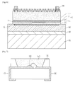
- FIG. 1 is a view showing a light-emitting device according to the embodiment.
- the light-emitting device may include a light-emitting structure 10, a reflective layer 17, a first electrode 50 and a second electrode 80.
- the light-emitting structure 10 may include a first conductive semiconductor layer 11, an active layer 12, and a second conductive semiconductor layer 13.
- the active layer 12 may be interposed between the first conductive semiconductor layer 11 and the second conductive semiconductor layer 13.
- the active layer 12 may be provided under the first conductive semiconductor layer 11, and the second conductive semiconductor layer 13 may be provided under the active layer 12.
- the first conductive semiconductor layer 11 may include an N-type semiconductor layer doped with N-type dopants serving as first conductive dopants
- the second conductive semiconductor layer 13 may include a P-type semiconductor layer doped with P-type dopants serving as second conductive dopants
- the first conductive semiconductor layer 11 may include a P-type semiconductor layer
- the second conductive semiconductor layer 13 may include an N-type semiconductor layer.
- the first conductive semiconductor layer 11 may include an N-type semiconductor layer.
- the first conductive semiconductor layer 11 may be realized by using a compound semiconductor.
- the first conductive semiconductor layer 11 may be realized by using a group II-VI compound semiconductor, or a group III-V compound semiconductor.
- the first conductive semiconductor layer 11 may be realized by using a semiconductor material having a compositional formula of In x Al y Ga 1-x-y N (0 ⁇ x ⁇ 1, 0 ⁇ y ⁇ 1, 0 ⁇ x+y ⁇ 1).
- the first conductive semiconductor layer 11 may include one selected from the group consisting of GaN, AIN, AlGaN, InGaN, InN, InAlGaN, AlInN, AlGaAs, GaP, GaAs, GaAsP, and AlGaInP doped with N-type dopants such as Si, Ge, Sn, Se, and Te.
- the active layer 12 emits light having a wavelength corresponding to the energy band gap difference according to materials constituting the active layer 12 through the combination of electrons (or holes) injected through the first conductive semiconductor layer 11 and holes (or electrons) injected through the second conductive semiconductor layer 13.
- the active layer 12 may have one of a single quantum well (SQW) structure, a multi-quantum well (MQW) structure, a quantum dot structure, and a quantum wire structure, but the embodiment is not limited thereto.
- the active layer 12 may be realized by using a compound semiconductor.
- the active layer 12 may be realized by using a semiconductor material having a compositional formula of InxAlyGa1-x-yN (0 ⁇ x ⁇ 1, 0 ⁇ y ⁇ 1, 0 ⁇ x+y ⁇ 1).
- the active layer 12 may be formed by stacking a plurality of well layers and a plurality of barrier layers.
- the active layer 12 may have a cycle of InGaN well layer/GaN barrier layer.
- the second conductive semiconductor layer 13 may include a P-type semiconductor layer.
- the second conductive semiconductor layer 13 may be realized by using a compound semiconductor.
- the second conductive semiconductor layer 13 may be realized by using a group II-VI compound semiconductor, or a group II-V compound semiconductor.
- the second conductive semiconductor layer 13 may be realized by using a semiconductor material having a compositional formula of InxAlyGa1-x-yN (0 ⁇ x ⁇ 1, 0 ⁇ y ⁇ 1, 0 ⁇ x+y ⁇ 1).
- the second conductive semiconductor layer 13 may include one selected from the group consisting of GaN, AIN, AlGaN, InGaN, InN, InAlGaN, AlInN, AlGaAs, GaP, GaAs, GaAsP, and AlGaInP doped with P-type dopants such as Mg, Zn, Ca, Sr, and Ba.
- the first conductive semiconductor layer 11 may include a P-type semiconductor layer and the second conductive semiconductor layer 13 may include the N-type semiconductor layer.
- a semiconductor layer including an N-type or P-type semiconductor layer may be additionally provided under the second conductive semiconductor layer 13.
- the first light-emitting structure 10 may have at least one of an NP junction structure, a PN junction structure, an NPN junction structure, or a PNP junction structure.
- impurities may be doped into the first conductive semiconductor layer 11 and the second conductive semiconductor layer 13 with uniform or non-uniform doping concentration.
- the first light-emitting structure 10 may have various structures, and the embodiment is not limited thereto.
- a first conductive InGaN/GaN superlattice structure or InGaN/InGaN superlattice structure may be formed between the first conductive semiconductor layer 11 and the active layer 12.
- a second conductive AlGaN layer may be formed between the second conductive semiconductor layer 13 and the active layer 12.
- the first electrode 50 may be disposed under the light-emitting structure 10.
- the first electrode 50 may be electrically connected to the second conductive semiconductor layer 13.
- the first electrode 50 may make contact with a bottom surface of the second conductive semiconductor layer 13.
- An ohmic contact layer 15 may be further disposed between the light-emitting structure 10 and the first electrode 50. A portion of the first electrode 50 may be disposed around the ohmic contact layer 15. A portion of the first electrode 50 may be disposed under the ohmic contact layer 15.
- a first region of the first electrode 50 may make contact with a bottom of the second conductive semiconductor layer 13 and a second region of the first electrode 50 may extend outward from the first region of the first electrode 50.
- the second region of the first electrode 50 may be exposed to a lower peripheral portion of the light-emitting structure 10.
- the ohmic contact layer 15 may include a transparent conductive oxide layer.
- the ohmic contact layer 15 may include at least one selected from the group consisting of an ITO (Indium Tin Oxide), an IZO (Indium Zinc Oxide), an AZO (Aluminum Zinc Oxide), an AGZO (Aluminum Gallium Zinc Oxide), an IZTO (Indium Zinc Tin Oxide), an IAZO (Indium Aluminum Zinc Oxide), an IGZO (Indium Gallium Zinc Oxide), an IGTO (Indium Gallium Tin Oxide), an ATO (Antimony Tin Oxide), a GZO (Gallium Zinc Oxide), an IZON (IZO Nitride), ZnO, IrOx, RuOx, NiO, Pt and Ag.
- the first electrode 50 may include at least one of Cu, Ni, Ti, Ti-W, Cr, W, Pt, V, Fe, and Mo.
- the first electrode 50 may serve as a diffusion barrier layer.
- a bonding layer 60 and a support member 70 may be disposed under the first electrode 50.
- the first electrode 50 may prevent a material included in the bonding layer 60 from being diffused to the ohmic contact layer 15 in the process of providing the bonding layer 60.
- the first electrode 50 may prevent a material, such as Sn, included in the bonding layer 60 from exerting an influence upon the ohmic contact layer 15.
- the bonding layer 60 may include barrier metal or bonding metal.
- the bonding layer 60 may include at least one of Ti, Au, Sn, Ni, Cr, Ga, In, Bi, Cu, Ag, Nb, Pd and Ta.
- the support member 70 may support the light-emitting structure 10 according to the embodiment while performing a heat radiation function.
- the bonding layer 60 may be realized in the form of a seed layer.
- the support member 70 may include at least one of semiconductor substrates (e.g., Si, Ge, GaN, GaAs, ZnO, SiC, and SiGe substrates) implanted with Ti, Cr, Ni, Al, Pt, Au, W, Cu, Mo, Cu-W, or impurities.
- the support member 70 may be formed of insulating material.
- the light-emitting device may include a reflective layer 17 disposed in the second conductive semiconductor layer 13.
- the reflective layer 17 may be spaced apart from the first electrode 50.
- the reflective layer 17 may be spaced apart from the active layer 12.
- the reflective layer 17 may have a thickness of 10 nm or more.
- the reflective layer 17 may have a thickness in the range of 10 nm to 100 nm.
- the reflective layer 17 may be sequentially grown when the second conductive semiconductor layer 13 is grown.
- the reflective layer 17 may be formed through an ion implantation process after the second conductive semiconductor layer 13 has been grown.
- the reflective layer 17 may include a conductive ion implantation layer.
- the reflective layer 17 may include one selected from the group consisting of Ag, Al, Pt and Rh.
- the second conductive semiconductor layer 13 may be divided into a second conductive first semiconductor layer 21 and a second conductive second semiconductor layer 22 by the reflective layer 17.
- the second conductive first semiconductor layer 21 may be disposed on the reflective layer 17.
- the second conductive first semiconductor layer 21 may make contact with a top surface of the reflective layer 17.
- the second conductive second semiconductor layer 22 may be disposed under the reflective layer 17.
- the second conductive second semiconductor layer 22 may make contact with a bottom surface of the reflective layer 17.
- the reflective layer 17 may be closer to the active layer 12 as compared with the first electrode 50.
- the second conductive first semiconductor layer 21 may have a thickness thinner than a thickness of the second conductive second semiconductor layer 22.
- the reflective layer 17 may be disposed within 100 nm from the bottom surface of the active layer 12.
- the reflective layer 17 since the reflective layer 17 is closer to the active layer 12, the reflective layer 17 may effectively reflect light emitted from the active layer 12.
- a semiconductor layer such as the second conductive semiconductor layer 13 may have defects when the crystal growth proceeds.
- the second conductive semiconductor layer 13 may absorb a part of light emitted from the active layer 12.
- the reflective layer 17 is disposed adjacent to the active layer 12, so that the light emitted from the active layer 12 may be effectively reflected by the reflective layer 17.
- the light-emitting device of the embodiment light absorption in the second conductive semiconductor layer 13 may be reduced, so that the light extraction efficiency can be improved.
- the reflective layer 17 may include a material having high reflectance.
- the reflective layer 17 may include a metal including at least one of Ag, Ni, Al, Rh, Pd, Ir, Ru, Mg, Zn, Pt, Cu, Au, and Hf, or an alloy thereof.
- the reflective layer 17 may be formed in a multi-layer of the metal or the alloy thereof and a transmissive conductive material such as an ITO (Indium-Tin-Oxide), an IZO (Indium-Zinc-Oxide), an IZTO (Indium-Zinc-Tin-Oxide), an IAZO (Indium-Aluminum-Zinc-Oxide), an IGZO (Indium-Gallium-Zinc-Oxide), an IGTO (Indium-Gallium-Tin-Oxide), an AZO (Aluminum-Zinc-Oxide), or an ATO (Antimony-Tin-Oxide).
- the reflective layer 17 may include at least one of Ag, Al, an Ag-Pd-Cu alloy, and an Ag-Cu alloy.
- An additional layer such as a diffusion barrier layer, may be formed on or under the reflective layer 17.
- the diffusion barrier layer formed on or under the reflective layer 17 may prevent materials contained in the reflective layer 17 from diffusing into the second conductive semiconductor layer 13.
- the light-emitting device may include the second electrode 80 electrically connected to the first conductive semiconductor layer 11.
- the second electrode 80 may be disposed on the first conductive semiconductor layer 11.
- the second electrode 80 may make contact with a top surface of the first conductive semiconductor layer 11.
- the second electrode 80 may be realized in the form of a multiple layer.
- the second electrode 80 may include an ohmic layer, an intermediate layer, and an upper layer.
- the ohmic layer may include a material selected from the group consisting of Cr, V, W, Ti, and Zn to realize ohmic contact.
- the intermediate layer may be realized by using a material selected from the group consisting of Ni, Cu, and Al.
- the upper layer may include Au.
- the second electrode 80 may include at least one selected from the group consisting of Cr, V, W, Ti, Zn, Ni, Cu, Al, and Au.
- a light extraction pattern may be provided on the top surface of the light-emitting structure 10.
- a concavo-convex pattern may be provided on the top surface of the light-emitting structure 10.
- the light extraction pattern provided on the light-emitting structure 10 may be formed through a PEC (photo electro chemical) etching process. Therefore, according to the embodiment, the light extraction effect to the outside can be increased.
- the first conductive semiconductor layer 11, the active layer 12, and the second conductive semiconductor layer 13 may be formed on a substrate 5.
- the first conductive semiconductor layer 11, the active layer 12, and the second conductive semiconductor layer 13 may be defined as the light-emitting structure 10
- the substrate 5 may include at least one of a sapphire substrate (Al 2 O 3 ), SiC, GaAs, GaN, ZnO, Si, GaP, InP, and Ge, but the embodiment is not limited thereto.
- a buffer layer may be interposed between the first conductive semiconductor layer 11 and the substrate 5.
- the first conductive semiconductor layer 11 may include an N-type semiconductor layer doped with N-type dopants serving as first conductive dopants
- the second conductive semiconductor layer 13 may include a P-type semiconductor layer doped with P-type dopants serving as second conductive dopants
- the first conductive semiconductor layer 11 may include a P-type semiconductor layer
- the second conductive semiconductor layer 13 may include an N-type semiconductor layer.
- the first conductive semiconductor layer 11 may include an N-type semiconductor.
- the first conductive semiconductor layer 11 may include a semiconductor material having a compositional formula of In x Al y Ga 1-x-y N (0 ⁇ x ⁇ 1, 0 ⁇ y ⁇ 1, 0 ⁇ x+y ⁇ 1).
- the first conductive semiconductor layer 11a may include one selected from the group consisting of InAlGaN, GaN, AlGaN, AlInN, InGaN, AIN, and InN, and may be doped with N-type dopants such as Si, Ge, Sn, Se, and Te.
- the active layer 12 emits light having a wavelength corresponding to the energy band gap difference according to materials constituting the active layer 12 through the combination of electrons (or holes) injected through the first conductive semiconductor layer 11 and holes (or electrons) injected through the second conductive semiconductor layer 13.
- the active layer 12 may have one of a single quantum well (SQW) structure, a multi-quantum well (MQW) structure, a quantum dot structure, and a quantum wire structure, but the embodiment is not limited thereto.
- the active layer 12 may be realized by using a semiconductor material having a compositional formula of In x Al y Ga 1-x-y N (0 ⁇ x ⁇ 1, 0 ⁇ y ⁇ 1, 0 ⁇ x+y ⁇ 1).
- the active layer 12 may be formed by stacking a plurality of well layers and a plurality of barrier layers.
- the active layer 12 may have a cycle of InGaN well layer/GaN barrier layer.
- the second conductive semiconductor layer 13 may be realized by using a P type semiconductor.
- the second conductive semiconductor layer 13 may be realized by using a semiconductor material having a compositional formula of In x Al y Ga 1-x-y N (0 ⁇ x ⁇ 1, 0 ⁇ y ⁇ 1, 0 ⁇ x+y ⁇ 1).
- the second conductive semiconductor layer 13 may include one selected from the group consisting of InAlGaN, GaN, AlGaN, InGaN, AlInN, AIN, and InN, and may be doped with P-type dopants such as Mg, Zn, Ca, Sr, and Ba.
- the first conductive semiconductor layer 11 may include a P-type semiconductor layer and the second conductive semiconductor layer 13 may include the N-type semiconductor layer.
- a semiconductor layer including an N-type or P-type semiconductor layer may be additionally provided on the second conductive semiconductor layer 13.
- the light-emitting structure 10 may have at least one of an NP junction structure, a PN junction structure, an NPN junction structure, or a PNP junction structure.
- impurities may be doped into the first conductive semiconductor layer 11 and the second conductive semiconductor layer 13 with uniform or non-uniform doping concentration.
- the light-emitting structure 10 may have various structures, and the embodiment is not limited thereto.
- first conductive InGaN/GaN superlattice structure or InGaN/InGaN superlattice structure may be formed between the first conductive semiconductor layer 11 and the active layer 12.
- a second conductive AlGaN layer may be formed between the second conductive semiconductor layer 13 and the active layer 12.
- the reflective layer 17 may be formed in the second conductive semiconductor layer 13.
- the reflective layer 17 may be formed through an ion implantation process.
- the reflective layer 17 may include a conductive ion implantation layer.
- the reflective layer 17 may have a thickness of 10 nm or more.
- the reflective layer 17 may have a thickness in the range of 10 nm to 100 nm.
- the reflective layer 17 may include one selected from the group consisting of Ag, Al, Pt and Rh.
- the second conductive semiconductor layer 13 may be divided into a second conductive first semiconductor layer 21 and a second conductive second semiconductor layer 22 by the reflective layer 17.
- the second conductive first semiconductor layer 21 may be disposed under the reflective layer 17.
- the second conductive first semiconductor layer 21 may make contact with a bottom surface of the reflective layer 17.
- the second conductive second semiconductor layer 22 may be disposed on the reflective layer 17.
- the second conductive second semiconductor layer 22 may make contact with a top surface of the reflective layer 17.
- the reflective layer 17 may be sequentially grown when the second conductive semiconductor layer 13 is grown.
- the second conductive first semiconductor layer 21, the reflective layer 17 and the second conductive second semiconductor layer 22 may be sequentially formed.
- the ohmic contact layer 15 and the first electrode 50 may be formed on the light-emitting structure 10.
- the ohmic contact layer 15 may include a transparent conductive oxide layer.
- the ohmic contact layer 15 may include at least one selected from the group consisting of an ITO (Indium Tin Oxide), an IZO (Indium Zinc Oxide), an AZO (Aluminum Zinc Oxide), an AGZO (Aluminum Gallium Zinc Oxide), an IZTO (Indium Zinc Tin Oxide), an IAZO (Indium Aluminum Zinc Oxide), an IGZO (Indium Gallium Zinc Oxide), an IGTO (Indium Gallium Tin Oxide), an ATO (Antimony Tin Oxide), a GZO (Gallium Zinc Oxide), an IZON (IZO Nitride), ZnO, IrOx, RuOx, NiO, Pt and Ag.
- the first electrode 50 may be electrically connected to the second conductive semiconductor layer 13.
- the first electrode 50 may make contact with a top surface of the second conductive semiconductor layer 13.
- a portion of the first electrode may be disposed around the ohmic contact layer 15.
- a portion of the first electrode may be disposed on the ohmic contact layer 15.
- the first electrode 50 may include at least one of Cu, Ni, TI, Ti-W, Cr, W, Pt, V, Fe, and Mo.
- the bonding layer 60 and the support member 70 may be provided on the first electrode 50.
- the first electrode 50 may serve as a diffusion barrier layer.
- the first electrode 50 may prevent a material included in the bonding layer 60 from being diffused toward the ohmic contact layer 15 in the process of providing the bonding layer 60.
- the first electrode 50 may prevent a material, such as Sn, included in the bonding layer 60 from exerting an influence upon the ohmic contact layer 15.
- the bonding layer 60 may include barrier metal or bonding metal.
- the bonding layer 60 may include at least one of Ti, Au, Sn, Ni, Cr, Ga, In, Bi, Cu, Ag, Nb, Pd and Ta.
- the support member 70 may support the light-emitting structure 10 according to the embodiment while performing a heat radiation function.
- the bonding layer 60 may be realized in the form of a seed layer.
- the support member 70 may include at least one of semiconductor substrates (e.g., Si, Ge, GaN, GaAs, ZnO, SiC, and SiGe substrates) implanted with Ti, Cr, Ni, Al, Pt, Au, W, Cu, Mo, Cu-W, or impurities.
- semiconductor substrates e.g., Si, Ge, GaN, GaAs, ZnO, SiC, and SiGe substrates
- the substrate 5 is removed from the first conductive semiconductor layer 11.
- the substrate 5 may be removed through a laser lift off (LLO) process.
- LLO process is a process to delaminate the substrate 5 from the first conductive semiconductor layer 11 by irradiating a laser to the bottom surface of the substrate 5.
- the lateral side of the light-emitting structure 10 is etched through an isolation etching process to expose a portion of the metal layer 30.
- the isolation etching process may be performed through a dry etching process such as an inductively coupled plasma (ICP) process, but the embodiment is not limited thereto.
- ICP inductively coupled plasma
- a light extraction pattern may be provided on the top surface of the light-emitting structure 10.
- a concavo-convex pattern may be provided on the top surface of the light-emitting structure 10.
- the light extraction pattern provided on the light-emitting structure 10 may be formed through a PEC (photo electro chemical) etching process. Therefore, according to the embodiment, the light extraction effect to the outside can be increased.
- the second electrode 80 electrically connected to the first conductive semiconductor layer 11 may be formed.
- the second electrode 80 may be disposed on the first conductive semiconductor layer 11.
- the second electrode 80 may make contact with a top surface of the first conductive semiconductor layer 11.
- the second electrode 80 may be realized in the form of a multiple layer.
- the second electrode 80 may include an ohmic layer, an intermediate layer, and an upper layer.
- the ohmic layer may include a material selected from the group consisting of Cr, V, W, Ti, and Zn to realize ohmic contact.
- the intermediate layer may be realized by using a material selected from the group consisting of Ni, Cu, and Al.
- the upper layer may include Au.
- the second electrode 80 may include at least one selected from the group consisting of Cr, V, W, Ti, Zn, Ni, Cu, Al, and Au.
- a first region of the first electrode 50 may make contact with a bottom of the second conductive semiconductor layer 13 and a second region of the first electrode 50 may extend outward from the first region of the first electrode 50.
- the second region of the first electrode 50 may be exposed to a lower peripheral portion of the light-emitting structure 10.
- the light-emitting device may include the reflective layer 17 disposed in the second conductive semiconductor layer 13.
- the reflective layer 17 may be spaced apart from the first electrode 50.
- the reflective layer 17 may be spaced apart from the active layer 12.
- the reflective layer 17 may be closer to the active layer 12 as compared with the first electrode 50.
- the second conductive first semiconductor layer 21 may have a thickness thinner than a thickness of the second conductive second semiconductor layer 22.
- the reflective layer 17 may be disposed within 100 nm from the bottom surface of the active layer 12.
- the reflective layer 17 since the reflective layer 17 is closer to the active layer 12, the reflective layer 17 may effectively reflect light emitted from the active layer 12.
- a semiconductor layer such as the second conductive semiconductor layer 13 may have defects when the crystal growth proceeds.
- the second conductive semiconductor layer 13 may absorb a part of light emitted from the active layer 12.
- the reflective layer 17 is disposed adjacent to the active layer 12, so that the light emitted from the active layer 12 may be effectively reflected by the reflective layer 17.
- the light-emitting device of the embodiment light absorption in the second conductive semiconductor layer 13 may be reduced, so that the light extraction efficiency can be improved.
- the reflective layer 17 may include a material having high reflectance.
- the reflective layer 17 may include a metal including at least one of Ag, Ni, Al, Rh, Pd, Ir, Ru, Mg, Zn, Pt, Cu, Au, and Hf, or an alloy thereof.
- the reflective layer 17 may be formed in a multi-layer of the metal or the alloy thereof and a transmissive conductive material such as an ITO (Indium-Tin-Oxide), an IZO (Indium-Zinc-Oxide), an IZTO (Indium-Zinc-Tin-Oxide), an IAZO (Indium-Aluminum-Zinc-Oxide), an IGZO (Indium-Gallium-Zinc-Oxide), an IGTO (Indium-Gallium-Tin-Oxide), an AZO (Aluminum-Zinc-Oxide), or an ATO (Antimony-Tin-Oxide).
- the reflective layer 17 may include at least one of Ag, Al, an Ag-Pd-Cu alloy, and an Ag-Cu alloy.
- An additional layer such as a diffusion barrier layer, may be formed on or under the reflective layer 17.
- the diffusion barrier layer formed on or under the reflective layer 17 may prevent materials contained in the reflective layer 17 from diffusing into the second conductive semiconductor layer 13.
- FIG. 7 is a view showing a light-emitting device package to which the light-emitting device according to the embodiment is applied.
- the light-emitting device package may include a body 120, first and second lead electrodes 131 and 132 formed on the body 120, a light-emitting device 100 provided on the body 120 and electrically connected to the first and second lead electrodes 131 and 132 and a molding member 140 that surrounds the light-emitting device 100.
- the body 120 may include silicon, synthetic resin or metallic material, and an inclined surface may be formed in the vicinity of the light-emitting device 100.
- the first and second lead electrodes 131 and 132 are electrically isolated from each other to supply power to the light-emitting device 100.
- the first and second lead electrode 131 and 132 can improve the light efficiency by reflecting the light emitted from the light-emitting device 100. Further, the first and second lead electrodes 131 and 132 may dissipate heat generated from the light-emitting device 100 to the outside.
- the light-emitting device 100 can be installed on the body 120 or the first or second lead electrode 131 or 132.
- the light-emitting device 100 may be electrically connected to the first and second lead electrodes 131 and 132 through one of a wire scheme, a flip-chip scheme, and a die-bonding scheme.
- the molding member 140 may surround the light-emitting device 100 to protect the light-emitting device 100.
- the molding member 140 may include phosphors to change the wavelength of the light emitted from the light-emitting device 100.
- a plurality of light-emitting device or light-emitting device packages according to the embodiment may be arrayed on a substrate, and an optical member including a lens, a light guide plate, a prism sheet, or a diffusion sheet may be provided on the optical path of the light emitted from the light-emitting device package.
- the light-emitting device package, the substrate, and the optical member may serve as a light unit.
- the light unit is realized in a top view type or a side view type and variously provided in display devices of a portable terminal and a laptop computer or a lighting apparatus and an indicator apparatus.
- a lighting apparatus according to another embodiment can include a light-emitting device, or a light-emitting device package according to the embodiment.
- the lighting apparatus may include a lamp, a signal lamp, an electric sign board and a headlight of a vehicle.
- the light-emitting device may be applied to the light unit.
- the light unit has a structure in which a plurality of light-emitting devices are arrayed.
- the light unit may include a display device as shown in FIGS. 8 and 9 and the lighting apparatus as shown in FIGS. 10 to 14 .
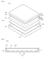
- a display device 1000 includes a light guide plate 1041, a light-emitting module 1031 for supplying the light to the light guide plate 1041, a reflective member 1022 provided below the light guide plate 1041, an optical sheet 1051 provided above the light guide plate 1041, a display panel 1061 provided above the optical sheet 1051, and a bottom cover 1011 for receiving the light guide plate 1041, the light-emitting module 1031, and the reflective member 1022.
- the embodiment is not limited to the above structure.
- the bottom cover 1011, the reflective member 1022, the light guide plate 1041 and the optical sheet 1051 may constitute a light unit 1050.
- the light guide plate 1041 diffuses the light to provide surface light.
- the light guide plate 1041 may include transparent material.
- the light guide plate 1041 may include one of acryl-based resin, such as PMMA (polymethyl methacrylate), PET (polyethylene terephthalate), PC (polycarbonate), COC (cyclic olefin copolymer) and PEN (polyethylene naphthalate) resin.
- PMMA polymethyl methacrylate
- PET polyethylene terephthalate
- PC polycarbonate
- COC cyclic olefin copolymer
- PEN polyethylene naphthalate
- the light-emitting module 1031 supplies the light to at least one side of the light guide plate 1041.
- the light-emitting module 1031 serves as the light source of the display device.
- At least one light-emitting module 1031 is provided to directly or indirectly supply the light from one side of the light guide plate 1041.
- the light-emitting module 1031 may include a substrate 1033 and light-emitting devices 100 or the light-emitting device package 200 according to the embodiment described above.
- the light-emitting packages 200 may be arrayed on the substrate 1033 while being spaced apart from each other at the predetermined interval.
- the substrate 1033 may be a printed circuit board (PCB) including a circuit pattern.
- the substrate 1033 may also include a metal core PCB (MCPCB) or a flexible PCB (FPCB) as well as the PCB, but the embodiment is not limited thereto. If the light-emitting device packages 200 are installed on the lateral side of the bottom cover 1011 or on a heat dissipation plate, the substrate 1033 may be omitted. The heat dissipation plate may partially make contact with the top surface of the bottom cover 1011.
- the light-emitting device packages 200 are installed such that light exit surfaces of the light-emitting device packages 200 are spaced apart from the light guide plate 1041 at a predetermined distance, but the embodiment is not limited thereto.
- the light-emitting device packages 200 may directly or indirectly supply the light to a light incident part, which is one side of the light guide plate 1041, but the embodiment is not limited thereto.
- the reflective member 1022 may be disposed below the light guide plate 1041.
- the reflective member 1022 reflects the light, which travels downward through the bottom surface of the light guide plate 1041, upward, thereby improving the brightness of the light unit 1050.
- the reflective member 1022 may include PET, PC or PVC resin, but the embodiment is not limited thereto.
- the reflective member 1022 may serve as the top surface of the bottom cover 1011, but the embodiment is not limited thereto.
- the bottom cover 1011 may receive the light guide plate 1041, the light-emitting module 1031, and the reflective member 1022 therein. To this end, the bottom cover 1011 has a receiving section 1012 having a box shape with an opened top surface, but the embodiment is not limited thereto. The bottom cover 1011 can be coupled with the top cover (not shown), but the embodiment is not limited thereto.
- the bottom cover 1011 can be manufactured through a press process or an extrusion process by using metallic material or resin material.
- the bottom cover 1011 may include metal or non-metallic material having superior thermal conductivity, but the embodiment is not limited thereto.
- the display panel 1061 for example, is an LCD panel including first and second transparent substrates, which are opposite to each other, and a liquid crystal layer interposed between the first and second substrates.
- a polarizing plate can be attached to at least one surface of the display panel 1061, but the embodiment is not limited thereto.
- the display panel 1061 displays information by using light passing through the optical sheet 1051.
- the display device 1000 can be applied to various portable terminals, monitors of notebook computers and laptop computers, and televisions.
- the optical sheet 1051 is disposed between the display panel 1061 and the light guide plate 1041 and includes at least one transmissive sheet.
- the optical sheet 1051 includes at least one of a diffusion sheet, horizontal and vertical prism sheets, and a brightness enhanced sheet.
- the diffusion sheet diffuses the incident light
- the horizontal and/or vertical prism sheet concentrates the incident light onto a display region
- the brightness enhanced sheet improves the brightness by reusing the light to be lost.
- a protective sheet can be provided on the display panel 1061, but the embodiment is not limited thereto.
- the light guide plate 1041 and the optical sheet 1051 can be provided on the optical path of the light-emitting module 1031 as optical members, but the embodiment is not limited thereto.
- FIG. 9 is a view showing another example of a display device according to the embodiment.
- the display device 1100 includes a bottom cover 1152, a substrate 1020 on which the light-emitting devices 100 are arrayed, an optical member 1154, and a display panel 1155.
- the substrate 1020 and the light-emitting device packages 200 may constitute a light-emitting module 1060.
- the bottom cover 1152, at least one light-emitting module 1060, and the optical member 154 may constitute a light unit.
- the bottom cover 1152 can be provided therein with a receiving section 1153, but the embodiment is not limited thereto.
- the optical member 1154 may include at least one of a lens, a light guide plate, a diffusion sheet, horizontal and vertical prism sheets, and a brightness enhanced sheet.
- the light guide plate may include PC or PMMA (Poly methyl methacrylate). The light guide plate can be omitted.
- the diffusion sheet diffuses the incident light
- the horizontal and vertical prism sheets concentrate the incident light onto a display region
- the brightness enhanced sheet improves the brightness by reusing the light to be lost.
- the optical member 1154 is disposed above the light-emitting module 1060 in order to convert the light emitted from the light-emitting module 1060 into the surface light. In addition, the optical member 1154 may diffuse or collect the light.
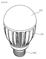
- FIGS. 10 to 12 are views showing a lighting apparatus according to the embodiment.
- FIG. 10 is a top perspective view of the lighting apparatus
- FIG. 11 is a bottom perspective view of the lighting apparatus shown in FIG. 10
- FIG. 12 is an exploded perspective view of the lighting apparatus shown in FIG. 10 .
- the lighting apparatus may include a cover 2100, a light source module 2200, a radiator 2400, a power supply part 2600, an inner case 2700, and a socket 2800.
- the lighting apparatus according to the embodiment may further include at least one of a member 2300 and a holder 2500.
- the light source module 2200 may include the light-emitting device package according to the embodiment.
- the cover 2100 may have a blub shape or a hemispheric shape.
- the cover 2100 may have a hollow structure which is partially open.
- the cover 2100 may be optically coupled with the light source module 2200.
- the cover 2100 may diffuse, scatter, or excite light provided from the light source module 2200.
- the cover 2100 may be an optical member.
- the cover 2100 may be coupled with the radiator 2400.
- the cover 2100 may include a coupling part which is coupled with the radiator 2400.
- the cover 2100 may include an inner surface coated with a milk-white pigment.
- the milk-white pigment may include a diffusion material to diffuse light.
- the roughness of the inner surface of the cover 2100 may be greater than the roughness of the outer surface of the cover 2100. The surface roughness is provided for the purpose of sufficiently scattering and diffusing the light from the light source module 2200.
- the cover 2100 may include glass, plastic, polypropylene (PP), polyethylene (PE) or polycarbonate (PC).
- the polycarbonate (PC) has the superior light resistance, heat resistance and strength among the above materials.
- the cover 2100 may be transparent so that a user may view the light source module 2200 from the outside, or may be opaque.
- the cover 2100 may be formed through a blow molding scheme.
- the light source module 220 may be disposed at one surface of the radiator 2400. Accordingly, the heat from the light source module 220 is transferred to the radiator 2400.
- the light source module 2200 may include a light source 2210, a connection plate 2230, and a connector 2250.
- the member 2300 is disposed on a top surface of the radiator 2400, and includes guide grooves 2310 into which a plurality of light sources 2210 and the connector 2250 are inserted.
- the guide grooves 2310 correspond to a substrate of the light source 2210 and the connector 2250.
- a surface of the member 2300 may be coated with a light reflective material.
- the surface of the member 2300 may be coated with white pigment.
- the member 2300 reflects again light, which is reflected by the inner surface of the cover 2100 and is returned to the direction of the light source module 2200, to the direction of the cover 2100. Accordingly, the light efficiency of the lighting apparatus according to the embodiment may be improved.
- the member 2300 may include an insulating material.
- the connection plate 2230 of the light source module 2200 may include an electrically conductive material.
- the radiator 2400 may be electrically connected to the connection plate 2230.
- the member 2300 may be formed by an insulating material, thereby preventing the connection plate 2230 from being electrically shorted with the radiator 2400.
- the radiator 2400 receives heat from the light source module 2200 and the power supply part 2600 and dissipates the heat.
- the holder 2500 covers a receiving groove 2719 of an insulating part 2710 of an inner case 2700. Accordingly, the power supply part 2600 received in the insulating part 2710 of the inner case 2700 is sealed.
- the holder 2500 includes a guide protrusion 2510.
- the guide protrusion 2510 has a hole and a protrusion of the power supply part 2600 extends by passing through the hole.
- the power supply part 2600 processes or converts an electric signal received from the outside and provides the processed or converted electric signal to the light source module 2200.
- the power supply part 2600 is received in the receiving groove 2719 of the inner case 2700, and is sealed inside the inner case 2700 by the holder 2500.
- the power supply part 2600 may include a protrusion 2610, a guide part 2630, a base 2650, and an extension part 2670.
- the guide part 2630 has a shape protruding from one side of the base 2650 to the outside.
- the guide part 2630 may be inserted into the holder 2500.
- a plurality of components may be disposed on one surface of the base 2650.
- the components may include a DC converter to convert AC power provided from an external power supply into DC power, a driving chip to control the driving of the light source module 2200, and an electrostatic discharge (ESD) protection device to protect the light source module 2200, but the embodiment is not limited thereto.
- the extension part 2670 has a shape protruding from an opposite side of the base 2650 to the outside.
- the extension part 2670 is inserted into an inside of the connection part 2750 of the inner case 2700, and receives an electric signal from the outside.
- a width of the extension part 2670 may be smaller than or equal to a width of the connection part 2750 of the inner case 2700.
- First terminals of a "+ electric wire” and a "- electric wire” are electrically connected to the extension part 2670 and second terminals of the "+ electric wire” and the "-electric wire” may be electrically connected to a socket 2800.
- the inner case 2700 may include a molding part therein together with the power supply part 2600.
- the molding part is prepared by hardening molding liquid, and the power supply part 2600 may be fixed inside the inner case 2700 by the molding part.
- FIGS. 13 and 14 are views showing another example of a lighting apparatus according to the embodiment.
- FIG. 13 is a perspective view of the lighting apparatus according to the embodiment and FIG. 14 is an exploded perspective view of the lighting apparatus shown in FIG. 13 .
- FIGS. 13 and 14 components and structures the same as those described with reference to FIGS. 10 to 12 will not be further described in order to avoid redundancy.
- the lighting apparatus may include a cover 3100, a light source part 3200, a radiator 3300, a circuit part 3400, an inner case 3500, and a socket 3600.
- the light source part 3200 may include the light-emitting device or the light-emitting device module according to the embodiment.
- the cover 3100 may have a hollow blub shape.
- the cover 3100 has an opening 3110.
- the light source part 3200 and a member 3350 may be inserted through the opening 3110.
- the cover 3100 may be coupled with the radiator 3300 and may surround the light source part 3200 and the member 3350.
- the light source part 3200 and the member 3350 may be blocked from the outside by the coupling between the cover 3100 and the radiator 3300.
- the cover 3100 may be coupled with the radiator 3300 by an adhesive or various schemes such as a rotation coupling scheme and a hook coupling scheme.
- the rotation coupling scheme is a scheme where a thread of the cover 3100 is coupled with a screw groove of the radiator 3300, and the cover 3100 is coupled with the radiator 3300 by rotation of the cover 3100.
- the hook coupling scheme is a scheme where a projection of the cover 3100 is inserted into a groove of the radiator 3300 so that the cover 3100 is coupled with the radiator 3300.
- the light source part 3200 is disposed at the member 3350 of the radiator 3300, and a plurality of light source parts 3200 may be provided.
- the light source part 3200 may be disposed on at least one of side surfaces of the member 3350.
- the light source part 3200 may be disposed at an upper portion of the side surface of the member 3350.
- the light source part 3200 may be disposed at three of six side surfaces of the member 3350. However, the embodiment is not limited thereto, and the light source part 3200 may be disposed at all side surfaces of the member 3350.
- the light source part 3200 may include a substrate 3210 and a light-emitting device 3230.
- the light-emitting device 3230 may be disposed on one surface of the substrate 3210.
- the substrate 3210 has a rectangular plate shape, but the embodiment is not limited thereto.
- the substrate 3210 may have various shapes.
- the substrate 3210 may have a circular plate shape or a polygonal plate shape.
- the substrate 3210 may be provided by printing a circuit pattern on an insulator.
- the substrate 3210 may include a typical printed circuit board (PCB), a metal core PCB, a flexible PCB, and a ceramic PCB.
- the substrate may have a COB (chips on board) type in which LED chips, which are not packaged, are directly bonded on the PCB.
- the substrate 3210 may include a material suitable to reflect light, or the surface of the substrate may have a color such as a white color or a silver color to effectively reflect the light.
- the substrate 3210 may be electrically connected to the circuit part 3400 received in the radiator 3300.
- the substrate 3210 and the circuit part 3400 may be connected to each other by a wire.
- the wire may connect the substrate 3210 and the circuit part 3400 to each other by passing through the radiator 3300.
- the light-emitting device 3230 may include a luminescence material.
- the luminescence material may include at least one of garnet-based phosphors (YAG, or TAG), silicate-based phosphors, nitride-based phosphors, and oxynitride-based phosphors.
- the luminescence material may include at least one of a red luminescence material, a yellow luminescence material and a green luminescence material.
- the radiator 3300 is coupled with the cover 3100, and may radiate heat from the light source part 3200.
- the radiator 330 has a predetermined volume, and includes a top surface 3310 and a side surface 3330.
- the member 3350 may be disposed on the top surface 3310 of the radiator 3310.
- the top surface 3310 of the radiator 3300 may be coupled with the cover 3100.
- the top surface 3310 of the radiator 3300 may have a shape corresponding to an opening 3110 of the cover 3100.
- a plurality of heat radiation pins 3370 may be disposed at the side surface 3330 of the radiator 3300.
- the heat radiation pin 3370 may extend outward from the side surface 3330 of the radiator 3300 or may be connected to the side surface 3330 of the radiator 3300.
- the heat radiation pin 3370 may improve heat radiation efficiency by increasing a heat radiation area of the radiator 3300.
- the side surface 3330 may not include the heat radiation pin 3370.
- the member 3350 may be disposed on the top surface of the radiator 3300.
- the member 3350 may be integrated with or coupled to the top surface 3310 of the radiator 3300.
- the member 3350 may have the shape of a polygonal prism.
- the member 3350 may have the shape of a hexahedral prism.
- the member 3350 having the shape of a hexahedral prism includes a top surface, a bottom surface, and six side surfaces.
- the member 3350 may have the shape of a circular prism or the shape of an elliptical prism as well as the shape of a hexahedral prism.
- the substrate 3210 of the light source part 3200 may be a flexible substrate.
- the light source part 3200 may be disposed at six side surfaces of the member 3350.
- the light source part 3200 may be disposed at all or some of the six side surfaces of the member 3350.
- the light source part 3200 is disposed at three of the six side surfaces of the member 3350.
- the substrate 3210 is disposed at the side surface of the member 3350.
- the side surface of the member 3350 may be substantially vertical to the top surface 3310 of the radiator 3300. Accordingly, the substrate 3210 and the top surface of the radiator 3300 may be substantially vertical to each other.
- the member 3350 may include a material representing thermal conductivity. Thus, heat from the light source part 3200 can be rapidly transferred to the member 3350.
- the material for the member 3350 may include an alloy of metals such as aluminum (Al), nickel (Ni), copper (Cu), magnesium (Mg), silver (Ag), or tin (Sn).
- the member 3350 may include a plastic material having thermal conductivity. The plastic material having thermal conductivity is advantageous in that it is lighter than the metal and has thermal conductivity in a single direction.
- the circuit part 3400 receives power from the outside, and converts the received power suitably for the light source part 3200.
- the circuit part 3400 provides the converted power to the light source part 3200.
- the circuit part 3400 may be disposed at the radiator 3300.
- the circuit part 3400 may be received in the inner case 3500, and may be received in the radiator 3300 together with the inner case 3500.
- the circuit part 3400 may include a circuit board 3410 and a plurality of components mounted on the circuit board 3410.
- the circuit board 3410 has a circular shape, but the embodiment is not limited thereto. That is, the circuit board 3410 may have various shapes. For example, the circuit board may have an elliptical shape or a polygonal shape.
- the circuit board 3410 may be provided by printing a circuit pattern on an insulator.
- the circuit board 3410 is electrically connected to the substrate 3210 of the light source part 3200.
- the circuit part 3410 and the substrate 3210 may be connected to each other by a wire.
- the wire may be disposed inside the radiator 3300 to connect the substrate 3210 to the circuit board 3410.
- a plurality of components 3430 may include a direct current converter converting AC power provided from an external power supply into DC power, a driving chip controlling driving of the light source part 3200, and an electrostatic discharge (ESD) protective device.
- ESD electrostatic discharge
- the inner case 3500 receives the circuit part 3400 therein.
- the inner case 3500 may include a receiving part 3510 to receive the circuit part 3400.
- the receiving part 3510 may have a cylindrical shape.
- the shape of the receiving part 3510 may be changed according to the shape of the radiator 3300.
- the inner case 3500 may be received in the radiator 3300.
- the receiving part 3510 of the inner case 3500 may be received in a receiving part which is formed at a bottom surface of the radiator 3300.
- the inner case 3500 may be coupled with the socket 3600.
- the inner case 3500 may include a connecting part 3530 coupled with the socket 3600.
- the connecting part 3530 may have a thread structure corresponding to a screw groove structure of the socket 3600.
- the inner case 3500 is an insulator. Accordingly, the inner case 3500 prevents electric short between the circuit part 3400 and the radiator 3300.
- the inner case 3500 may include a plastic or resin material.
- the socket 3600 may be coupled with the inner case 3500.
- the socket 3600 may be coupled with the connecting part 3530 of the inner case 3500.
- the socket 3600 may have the structure the same as that of a conventional incandescent light bulb.
- the socket 3600 is electrically connected to the circuit part 3400.
- the circuit part 3400 and the socket 3600 may be connected to each other by a wire. If external power is applied to the socket 3600, the external power may be transferred to the circuit part 3400.
- the socket 3600 may have a screw groove structure corresponding to a thread structure of the connecting part 3550.
- any reference in this specification to "one embodiment,” “an embodiment,” “example embodiment,” etc. means that a particular feature, structure, or characteristic described in connection with the embodiment is included in at least one embodiment of the invention.
- the appearances of such phrases in various places in the specification are not necessarily all referring to the same embodiment.
Landscapes
- Led Devices (AREA)
- Led Device Packages (AREA)
Abstract
Description
- This application claims under 35 U.S.C. § 119 to Korean Patent Application No.
10-2012-0061376 filed on June 8, 2012 - The embodiment relates to a light-emitting device, a light-emitting device package, and a light unit.
- A light-emitting diode (LED) has been extensively used as one of light-emitting devices. The LED converts electrical signals into the form of light such as infra-red light, ultra-violet light, and visible light by using the characteristic of a compound semiconductor.
- As the light efficiency of the light-emitting device is increased, the LED has been used in various fields such as display apparatuses and lighting appliances.
- The embodiment provides a light-emitting device, a light-emitting device package, and a light unit, capable of improving light extraction efficiency.
- A light-emitting device according to the embodiment includes a light-emitting structure including a first conductive semiconductor layer, an active layer under the first conductive semiconductor layer, and a second conductive semiconductor layer under the active layer; a first electrode arranged under the light-emitting structure and electrically connected to the second conductive semiconductor layer; a reflective layer arranged inside the second conductive semiconductor layer and spaced apart from the first electrode and the active layer; and a second electrode electrically connected to the first conductive semiconductor layer.
- A light-emitting device package according to the embodiment includes a body; a light-emitting device on the body; and first and second lead electrodes electrically connected to the light-emitting device, wherein the light-emitting device includes a light-emitting structure including a first conductive semiconductor layer, an active layer under the first conductive semiconductor layer, and a second conductive semiconductor layer under the active layer; a first electrode arranged under the light-emitting structure and electrically connected to the second conductive semiconductor layer; a reflective layer arranged inside the second conductive semiconductor layer and spaced apart from the first electrode and the active layer; and a second electrode electrically connected to the first conductive semiconductor layer.
- A light unit according to the embodiment includes a substrate; a light-emitting device on the substrate; and an optical member serving as an optical path for light emitted from the light-emitting device, wherein the light-emitting device includes a light-emitting structure including a first conductive semiconductor layer, an active layer under the first conductive semiconductor layer, and a second conductive semiconductor layer under the active layer; a first electrode arranged under the light-emitting structure and electrically connected to the second conductive semiconductor layer; a reflective layer arranged inside the second conductive semiconductor layer and spaced apart from the first electrode and the active layer; and a second electrode electrically connected to the first conductive semiconductor layer.
- The light-emitting device, the light-emitting device package, and the light unit according to the embodiment can improve the light extraction efficiency.
-
-
FIG. 1 is a view showing a light-emitting device according to the embodiment. -
FIGS. 2 to 6 are views showing a method of fabricating a light-emitting device according to the embodiment. -
FIG. 7 is a view showing a light-emitting device package according to the embodiment. -
FIG. 8 is a view showing a display device according to the embodiment. -
FIG. 9 is a view showing another example of the display device according to the embodiment. -
FIGS. 10 to 12 are views showing a lighting apparatus according to the embodiment. -
FIGS. 13 and14 are views showing another example of a lighting apparatus according to the embodiment. - In the description of the embodiments, it will be understood that, when a layer (or film), a region, a pattern, or a structure is referred to as being "on" or "under" another substrate, another layer (or film), another region, another pad, or another pattern, it can be "directly" or "indirectly" over the other substrate, layer (or film), region, pad, or pattern, or one or more intervening layers may also be present. Such a position of the layer has been described with reference to the drawings.
- The thickness and size of each layer shown in the drawings may be exaggerated, omitted or schematically drawn for the purpose of convenience or clarity. In addition, the size of elements does not utterly reflect an actual size.
- Hereinafter, a light-emitting device, a light-emitting device package, a light unit, and a method for fabricating the light-emitting device according to the embodiments will be described in detail with reference to accompanying drawings.
-
FIG. 1 is a view showing a light-emitting device according to the embodiment. - As shown in
FIG. 1 , the light-emitting device according to the embodiment may include a light-emitting structure 10, areflective layer 17, afirst electrode 50 and asecond electrode 80. - The light-
emitting structure 10 may include a firstconductive semiconductor layer 11, anactive layer 12, and a secondconductive semiconductor layer 13. Theactive layer 12 may be interposed between the firstconductive semiconductor layer 11 and the secondconductive semiconductor layer 13. Theactive layer 12 may be provided under the firstconductive semiconductor layer 11, and the secondconductive semiconductor layer 13 may be provided under theactive layer 12. - For instance, the first
conductive semiconductor layer 11 may include an N-type semiconductor layer doped with N-type dopants serving as first conductive dopants, and the secondconductive semiconductor layer 13 may include a P-type semiconductor layer doped with P-type dopants serving as second conductive dopants. In addition, the firstconductive semiconductor layer 11 may include a P-type semiconductor layer, and the secondconductive semiconductor layer 13 may include an N-type semiconductor layer. - For example, the first
conductive semiconductor layer 11 may include an N-type semiconductor layer. The firstconductive semiconductor layer 11 may be realized by using a compound semiconductor. The firstconductive semiconductor layer 11 may be realized by using a group II-VI compound semiconductor, or a group III-V compound semiconductor. - For example, the first
conductive semiconductor layer 11 may be realized by using a semiconductor material having a compositional formula of InxAlyGa1-x-yN (0≤x≤1, 0 ≤y≤1, 0≤x+y≤1). For example, the firstconductive semiconductor layer 11 may include one selected from the group consisting of GaN, AIN, AlGaN, InGaN, InN, InAlGaN, AlInN, AlGaAs, GaP, GaAs, GaAsP, and AlGaInP doped with N-type dopants such as Si, Ge, Sn, Se, and Te. - The
active layer 12 emits light having a wavelength corresponding to the energy band gap difference according to materials constituting theactive layer 12 through the combination of electrons (or holes) injected through the firstconductive semiconductor layer 11 and holes (or electrons) injected through the secondconductive semiconductor layer 13. Theactive layer 12 may have one of a single quantum well (SQW) structure, a multi-quantum well (MQW) structure, a quantum dot structure, and a quantum wire structure, but the embodiment is not limited thereto. - The
active layer 12 may be realized by using a compound semiconductor. Theactive layer 12 may be realized by using a semiconductor material having a compositional formula of InxAlyGa1-x-yN (0≤ x ≤ 1, 0 ≤ y ≤ 1, 0 ≤ x+y ≤ 1). When theactive layer 12 has an MQW structure, theactive layer 12 may be formed by stacking a plurality of well layers and a plurality of barrier layers. For example, theactive layer 12 may have a cycle of InGaN well layer/GaN barrier layer. - For example, the second
conductive semiconductor layer 13 may include a P-type semiconductor layer. The secondconductive semiconductor layer 13 may be realized by using a compound semiconductor. For example, the secondconductive semiconductor layer 13 may be realized by using a group II-VI compound semiconductor, or a group II-V compound semiconductor. - For example, the second
conductive semiconductor layer 13 may be realized by using a semiconductor material having a compositional formula of InxAlyGa1-x-yN (0≤x≤1, 0≤y≤1, 0≤x+y≤1). For example, the secondconductive semiconductor layer 13 may include one selected from the group consisting of GaN, AIN, AlGaN, InGaN, InN, InAlGaN, AlInN, AlGaAs, GaP, GaAs, GaAsP, and AlGaInP doped with P-type dopants such as Mg, Zn, Ca, Sr, and Ba. - Meanwhile, the first
conductive semiconductor layer 11 may include a P-type semiconductor layer and the secondconductive semiconductor layer 13 may include the N-type semiconductor layer. In addition, a semiconductor layer including an N-type or P-type semiconductor layer may be additionally provided under the secondconductive semiconductor layer 13. Accordingly, the first light-emitting structure 10 may have at least one of an NP junction structure, a PN junction structure, an NPN junction structure, or a PNP junction structure. In addition, impurities may be doped into the firstconductive semiconductor layer 11 and the secondconductive semiconductor layer 13 with uniform or non-uniform doping concentration. In other words, the first light-emittingstructure 10 may have various structures, and the embodiment is not limited thereto. - In addition, a first conductive InGaN/GaN superlattice structure or InGaN/InGaN superlattice structure may be formed between the first
conductive semiconductor layer 11 and theactive layer 12. In addition, a second conductive AlGaN layer may be formed between the secondconductive semiconductor layer 13 and theactive layer 12. - The
first electrode 50 may be disposed under the light-emittingstructure 10. Thefirst electrode 50 may be electrically connected to the secondconductive semiconductor layer 13. Thefirst electrode 50 may make contact with a bottom surface of the secondconductive semiconductor layer 13. - An
ohmic contact layer 15 may be further disposed between the light-emitting structure 10 and thefirst electrode 50. A portion of thefirst electrode 50 may be disposed around theohmic contact layer 15. A portion of thefirst electrode 50 may be disposed under theohmic contact layer 15. - In addition, a first region of the
first electrode 50 may make contact with a bottom of the secondconductive semiconductor layer 13 and a second region of thefirst electrode 50 may extend outward from the first region of thefirst electrode 50. The second region of thefirst electrode 50 may be exposed to a lower peripheral portion of the light-emittingstructure 10. - For example, the
ohmic contact layer 15 may include a transparent conductive oxide layer. For example, theohmic contact layer 15 may include at least one selected from the group consisting of an ITO (Indium Tin Oxide), an IZO (Indium Zinc Oxide), an AZO (Aluminum Zinc Oxide), an AGZO (Aluminum Gallium Zinc Oxide), an IZTO (Indium Zinc Tin Oxide), an IAZO (Indium Aluminum Zinc Oxide), an IGZO (Indium Gallium Zinc Oxide), an IGTO (Indium Gallium Tin Oxide), an ATO (Antimony Tin Oxide), a GZO (Gallium Zinc Oxide), an IZON (IZO Nitride), ZnO, IrOx, RuOx, NiO, Pt and Ag. - The
first electrode 50 may include at least one of Cu, Ni, Ti, Ti-W, Cr, W, Pt, V, Fe, and Mo. Thefirst electrode 50 may serve as a diffusion barrier layer. Abonding layer 60 and asupport member 70 may be disposed under thefirst electrode 50. - The
first electrode 50 may prevent a material included in thebonding layer 60 from being diffused to theohmic contact layer 15 in the process of providing thebonding layer 60. Thefirst electrode 50 may prevent a material, such as Sn, included in thebonding layer 60 from exerting an influence upon theohmic contact layer 15. - The
bonding layer 60 may include barrier metal or bonding metal. For example, thebonding layer 60 may include at least one of Ti, Au, Sn, Ni, Cr, Ga, In, Bi, Cu, Ag, Nb, Pd and Ta. Thesupport member 70 may support the light-emittingstructure 10 according to the embodiment while performing a heat radiation function. Thebonding layer 60 may be realized in the form of a seed layer. - The
support member 70 may include at least one of semiconductor substrates (e.g., Si, Ge, GaN, GaAs, ZnO, SiC, and SiGe substrates) implanted with Ti, Cr, Ni, Al, Pt, Au, W, Cu, Mo, Cu-W, or impurities. For example, thesupport member 70 may be formed of insulating material. - The light-emitting device according to the embodiment may include a
reflective layer 17 disposed in the secondconductive semiconductor layer 13. Thereflective layer 17 may be spaced apart from thefirst electrode 50. Thereflective layer 17 may be spaced apart from theactive layer 12. - The
reflective layer 17 may have a thickness of 10 nm or more. For instance, thereflective layer 17 may have a thickness in the range of 10 nm to 100 nm. Thereflective layer 17 may be sequentially grown when the secondconductive semiconductor layer 13 is grown. In addition, thereflective layer 17 may be formed through an ion implantation process after the secondconductive semiconductor layer 13 has been grown. For instance, thereflective layer 17 may include a conductive ion implantation layer. Thereflective layer 17 may include one selected from the group consisting of Ag, Al, Pt and Rh. - The second
conductive semiconductor layer 13 may be divided into a second conductivefirst semiconductor layer 21 and a second conductivesecond semiconductor layer 22 by thereflective layer 17. The second conductivefirst semiconductor layer 21 may be disposed on thereflective layer 17. The second conductivefirst semiconductor layer 21 may make contact with a top surface of thereflective layer 17. The second conductivesecond semiconductor layer 22 may be disposed under thereflective layer 17. The second conductivesecond semiconductor layer 22 may make contact with a bottom surface of thereflective layer 17. - The
reflective layer 17 may be closer to theactive layer 12 as compared with thefirst electrode 50. The second conductivefirst semiconductor layer 21 may have a thickness thinner than a thickness of the second conductivesecond semiconductor layer 22. For instance, thereflective layer 17 may be disposed within 100 nm from the bottom surface of theactive layer 12. - According to the embodiment, since the
reflective layer 17 is closer to theactive layer 12, thereflective layer 17 may effectively reflect light emitted from theactive layer 12. In general, a semiconductor layer, such as the secondconductive semiconductor layer 13, may have defects when the crystal growth proceeds. Thus, the secondconductive semiconductor layer 13 may absorb a part of light emitted from theactive layer 12. - According to the embodiment, the
reflective layer 17 is disposed adjacent to theactive layer 12, so that the light emitted from theactive layer 12 may be effectively reflected by thereflective layer 17. Thus, according to the light-emitting device of the embodiment, light absorption in the secondconductive semiconductor layer 13 may be reduced, so that the light extraction efficiency can be improved. - The
reflective layer 17 may include a material having high reflectance. For example, thereflective layer 17 may include a metal including at least one of Ag, Ni, Al, Rh, Pd, Ir, Ru, Mg, Zn, Pt, Cu, Au, and Hf, or an alloy thereof. In addition, thereflective layer 17 may be formed in a multi-layer of the metal or the alloy thereof and a transmissive conductive material such as an ITO (Indium-Tin-Oxide), an IZO (Indium-Zinc-Oxide), an IZTO (Indium-Zinc-Tin-Oxide), an IAZO (Indium-Aluminum-Zinc-Oxide), an IGZO (Indium-Gallium-Zinc-Oxide), an IGTO (Indium-Gallium-Tin-Oxide), an AZO (Aluminum-Zinc-Oxide), or an ATO (Antimony-Tin-Oxide). For example, according to the embodiment, thereflective layer 17 may include at least one of Ag, Al, an Ag-Pd-Cu alloy, and an Ag-Cu alloy. - An additional layer, such as a diffusion barrier layer, may be formed on or under the
reflective layer 17. The diffusion barrier layer formed on or under thereflective layer 17 may prevent materials contained in thereflective layer 17 from diffusing into the secondconductive semiconductor layer 13. - The light-emitting device according to the embodiment may include the
second electrode 80 electrically connected to the firstconductive semiconductor layer 11. For instance, thesecond electrode 80 may be disposed on the firstconductive semiconductor layer 11. Thesecond electrode 80 may make contact with a top surface of the firstconductive semiconductor layer 11. - According to the embodiment, power may be applied to the light-emitting
structure 10 through the first andsecond electrodes second electrode 80 may be realized in the form of a multiple layer. Thesecond electrode 80 may include an ohmic layer, an intermediate layer, and an upper layer. The ohmic layer may include a material selected from the group consisting of Cr, V, W, Ti, and Zn to realize ohmic contact. The intermediate layer may be realized by using a material selected from the group consisting of Ni, Cu, and Al. For example, the upper layer may include Au. Thesecond electrode 80 may include at least one selected from the group consisting of Cr, V, W, Ti, Zn, Ni, Cu, Al, and Au. - A light extraction pattern may be provided on the top surface of the light-emitting
structure 10. A concavo-convex pattern may be provided on the top surface of the light-emittingstructure 10. For example, the light extraction pattern provided on the light-emittingstructure 10 may be formed through a PEC (photo electro chemical) etching process. Therefore, according to the embodiment, the light extraction effect to the outside can be increased. - Hereinafter, a method of fabricating the light-emitting device according to the embodiment will be described with reference to
FIGS. 2 to 6 . - According to the method of fabricating the light-emitting device of the embodiment, as shown in
FIG. 2 , the firstconductive semiconductor layer 11, theactive layer 12, and the secondconductive semiconductor layer 13 may be formed on asubstrate 5. The firstconductive semiconductor layer 11, theactive layer 12, and the secondconductive semiconductor layer 13 may be defined as the light-emittingstructure 10 - For example, the
substrate 5 may include at least one of a sapphire substrate (Al2O3), SiC, GaAs, GaN, ZnO, Si, GaP, InP, and Ge, but the embodiment is not limited thereto. A buffer layer may be interposed between the firstconductive semiconductor layer 11 and thesubstrate 5. - For example, the first
conductive semiconductor layer 11 may include an N-type semiconductor layer doped with N-type dopants serving as first conductive dopants, and the secondconductive semiconductor layer 13 may include a P-type semiconductor layer doped with P-type dopants serving as second conductive dopants. In addition, the firstconductive semiconductor layer 11 may include a P-type semiconductor layer, and the secondconductive semiconductor layer 13 may include an N-type semiconductor layer. - For example, the first
conductive semiconductor layer 11 may include an N-type semiconductor. The firstconductive semiconductor layer 11 may include a semiconductor material having a compositional formula of InxAlyGa1-x-yN (0≤x≤1, 0 ≤y≤1, 0≤x+y≤1). For example, the first conductive semiconductor layer 11a may include one selected from the group consisting of InAlGaN, GaN, AlGaN, AlInN, InGaN, AIN, and InN, and may be doped with N-type dopants such as Si, Ge, Sn, Se, and Te. - The
active layer 12 emits light having a wavelength corresponding to the energy band gap difference according to materials constituting theactive layer 12 through the combination of electrons (or holes) injected through the firstconductive semiconductor layer 11 and holes (or electrons) injected through the secondconductive semiconductor layer 13. Theactive layer 12 may have one of a single quantum well (SQW) structure, a multi-quantum well (MQW) structure, a quantum dot structure, and a quantum wire structure, but the embodiment is not limited thereto. - The
active layer 12 may be realized by using a semiconductor material having a compositional formula of InxAlyGa1-x-yN (0≤ x ≤ 1, 0 ≤ y ≤ 1, 0 ≤ x+y ≤ 1). When theactive layer 12 has an MQW structure, theactive layer 12 may be formed by stacking a plurality of well layers and a plurality of barrier layers. For example, theactive layer 12 may have a cycle of InGaN well layer/GaN barrier layer. - For example, the second
conductive semiconductor layer 13 may be realized by using a P type semiconductor. The secondconductive semiconductor layer 13 may be realized by using a semiconductor material having a compositional formula of InxAlyGa1-x-yN (0≤x≤1, 0≤y≤1, 0≤x+y≤1). For example, the secondconductive semiconductor layer 13 may include one selected from the group consisting of InAlGaN, GaN, AlGaN, InGaN, AlInN, AIN, and InN, and may be doped with P-type dopants such as Mg, Zn, Ca, Sr, and Ba. - Meanwhile, the first
conductive semiconductor layer 11 may include a P-type semiconductor layer and the secondconductive semiconductor layer 13 may include the N-type semiconductor layer. In addition, a semiconductor layer including an N-type or P-type semiconductor layer may be additionally provided on the secondconductive semiconductor layer 13. Accordingly, the light-emittingstructure 10 may have at least one of an NP junction structure, a PN junction structure, an NPN junction structure, or a PNP junction structure. In addition, impurities may be doped into the firstconductive semiconductor layer 11 and the secondconductive semiconductor layer 13 with uniform or non-uniform doping concentration. In other words, the light-emittingstructure 10 may have various structures, and the embodiment is not limited thereto. - In addition, the first conductive InGaN/GaN superlattice structure or InGaN/InGaN superlattice structure may be formed between the first
conductive semiconductor layer 11 and theactive layer 12. In addition, a second conductive AlGaN layer may be formed between the secondconductive semiconductor layer 13 and theactive layer 12. - Next, as shown in
FIG. 3 , thereflective layer 17 may be formed in the secondconductive semiconductor layer 13. For instance, thereflective layer 17 may be formed through an ion implantation process. Thereflective layer 17 may include a conductive ion implantation layer. - The
reflective layer 17 may have a thickness of 10 nm or more. For instance, thereflective layer 17 may have a thickness in the range of 10 nm to 100 nm. Thereflective layer 17 may include one selected from the group consisting of Ag, Al, Pt and Rh. - The second
conductive semiconductor layer 13 may be divided into a second conductivefirst semiconductor layer 21 and a second conductivesecond semiconductor layer 22 by thereflective layer 17. The second conductivefirst semiconductor layer 21 may be disposed under thereflective layer 17. The second conductivefirst semiconductor layer 21 may make contact with a bottom surface of thereflective layer 17. The second conductivesecond semiconductor layer 22 may be disposed on thereflective layer 17. The second conductivesecond semiconductor layer 22 may make contact with a top surface of thereflective layer 17. - Meanwhile, the
reflective layer 17 may be sequentially grown when the secondconductive semiconductor layer 13 is grown. In other words, the second conductivefirst semiconductor layer 21, thereflective layer 17 and the second conductivesecond semiconductor layer 22 may be sequentially formed. - In addition, as shown in
FIG. 4 , theohmic contact layer 15 and thefirst electrode 50 may be formed on the light-emittingstructure 10. - For example, the
ohmic contact layer 15 may include a transparent conductive oxide layer. For example, theohmic contact layer 15 may include at least one selected from the group consisting of an ITO (Indium Tin Oxide), an IZO (Indium Zinc Oxide), an AZO (Aluminum Zinc Oxide), an AGZO (Aluminum Gallium Zinc Oxide), an IZTO (Indium Zinc Tin Oxide), an IAZO (Indium Aluminum Zinc Oxide), an IGZO (Indium Gallium Zinc Oxide), an IGTO (Indium Gallium Tin Oxide), an ATO (Antimony Tin Oxide), a GZO (Gallium Zinc Oxide), an IZON (IZO Nitride), ZnO, IrOx, RuOx, NiO, Pt and Ag. - The
first electrode 50 may be electrically connected to the secondconductive semiconductor layer 13. Thefirst electrode 50 may make contact with a top surface of the secondconductive semiconductor layer 13. A portion of the first electrode may be disposed around theohmic contact layer 15. A portion of the first electrode may be disposed on theohmic contact layer 15. Thefirst electrode 50 may include at least one of Cu, Ni, TI, Ti-W, Cr, W, Pt, V, Fe, and Mo. - Then, as shown in
FIG. 5 , thebonding layer 60 and thesupport member 70 may be provided on thefirst electrode 50. Thefirst electrode 50 may serve as a diffusion barrier layer. Thefirst electrode 50 may prevent a material included in thebonding layer 60 from being diffused toward theohmic contact layer 15 in the process of providing thebonding layer 60. Thefirst electrode 50 may prevent a material, such as Sn, included in thebonding layer 60 from exerting an influence upon theohmic contact layer 15. - The
bonding layer 60 may include barrier metal or bonding metal. For example, thebonding layer 60 may include at least one of Ti, Au, Sn, Ni, Cr, Ga, In, Bi, Cu, Ag, Nb, Pd and Ta. Thesupport member 70 may support the light-emittingstructure 10 according to the embodiment while performing a heat radiation function. Thebonding layer 60 may be realized in the form of a seed layer. - The
support member 70 may include at least one of semiconductor substrates (e.g., Si, Ge, GaN, GaAs, ZnO, SiC, and SiGe substrates) implanted with Ti, Cr, Ni, Al, Pt, Au, W, Cu, Mo, Cu-W, or impurities. - Next, the
substrate 5 is removed from the firstconductive semiconductor layer 11. According to one example, thesubstrate 5 may be removed through a laser lift off (LLO) process. The LLO process is a process to delaminate thesubstrate 5 from the firstconductive semiconductor layer 11 by irradiating a laser to the bottom surface of thesubstrate 5. - Then, as shown in
FIG. 6 , the lateral side of the light-emittingstructure 10 is etched through an isolation etching process to expose a portion of the metal layer 30. The isolation etching process may be performed through a dry etching process such as an inductively coupled plasma (ICP) process, but the embodiment is not limited thereto. - In addition, as shown in
FIG. 6 , a light extraction pattern may be provided on the top surface of the light-emittingstructure 10. A concavo-convex pattern may be provided on the top surface of the light-emittingstructure 10. For example, the light extraction pattern provided on the light-emittingstructure 10 may be formed through a PEC (photo electro chemical) etching process. Therefore, according to the embodiment, the light extraction effect to the outside can be increased. - In addition, as shown in
FIG. 6 , thesecond electrode 80 electrically connected to the firstconductive semiconductor layer 11 may be formed. For instance, thesecond electrode 80 may be disposed on the firstconductive semiconductor layer 11. Thesecond electrode 80 may make contact with a top surface of the firstconductive semiconductor layer 11. - According to the embodiment, power may be applied to the light-emitting
structure 10 through the first andsecond electrodes second electrode 80 may be realized in the form of a multiple layer. Thesecond electrode 80 may include an ohmic layer, an intermediate layer, and an upper layer. The ohmic layer may include a material selected from the group consisting of Cr, V, W, Ti, and Zn to realize ohmic contact. The intermediate layer may be realized by using a material selected from the group consisting of Ni, Cu, and Al. For example, the upper layer may include Au. Thesecond electrode 80 may include at least one selected from the group consisting of Cr, V, W, Ti, Zn, Ni, Cu, Al, and Au. - In addition, a first region of the
first electrode 50 may make contact with a bottom of the secondconductive semiconductor layer 13 and a second region of thefirst electrode 50 may extend outward from the first region of thefirst electrode 50. The second region of thefirst electrode 50 may be exposed to a lower peripheral portion of the light-emittingstructure 10. - The light-emitting device according to the embodiment may include the
reflective layer 17 disposed in the secondconductive semiconductor layer 13. Thereflective layer 17 may be spaced apart from thefirst electrode 50. Thereflective layer 17 may be spaced apart from theactive layer 12. - The
reflective layer 17 may be closer to theactive layer 12 as compared with thefirst electrode 50. The second conductivefirst semiconductor layer 21 may have a thickness thinner than a thickness of the second conductivesecond semiconductor layer 22. For instance, thereflective layer 17 may be disposed within 100 nm from the bottom surface of theactive layer 12. - According to the embodiment, since the
reflective layer 17 is closer to theactive layer 12, thereflective layer 17 may effectively reflect light emitted from theactive layer 12. In general, a semiconductor layer, such as the secondconductive semiconductor layer 13, may have defects when the crystal growth proceeds. Thus, the secondconductive semiconductor layer 13 may absorb a part of light emitted from theactive layer 12. - According to the embodiment, the
reflective layer 17 is disposed adjacent to theactive layer 12, so that the light emitted from theactive layer 12 may be effectively reflected by thereflective layer 17. Thus, according to the light-emitting device of the embodiment, light absorption in the secondconductive semiconductor layer 13 may be reduced, so that the light extraction efficiency can be improved. - The
reflective layer 17 may include a material having high reflectance. For example, thereflective layer 17 may include a metal including at least one of Ag, Ni, Al, Rh, Pd, Ir, Ru, Mg, Zn, Pt, Cu, Au, and Hf, or an alloy thereof. In addition, thereflective layer 17 may be formed in a multi-layer of the metal or the alloy thereof and a transmissive conductive material such as an ITO (Indium-Tin-Oxide), an IZO (Indium-Zinc-Oxide), an IZTO (Indium-Zinc-Tin-Oxide), an IAZO (Indium-Aluminum-Zinc-Oxide), an IGZO (Indium-Gallium-Zinc-Oxide), an IGTO (Indium-Gallium-Tin-Oxide), an AZO (Aluminum-Zinc-Oxide), or an ATO (Antimony-Tin-Oxide). For example, according to the embodiment, thereflective layer 17 may include at least one of Ag, Al, an Ag-Pd-Cu alloy, and an Ag-Cu alloy. - An additional layer, such as a diffusion barrier layer, may be formed on or under the
reflective layer 17. The diffusion barrier layer formed on or under thereflective layer 17 may prevent materials contained in thereflective layer 17 from diffusing into the secondconductive semiconductor layer 13. -
FIG. 7 is a view showing a light-emitting device package to which the light-emitting device according to the embodiment is applied. - Referring to
FIG. 7 , the light-emitting device package according to the embodiment may include abody 120, first and secondlead electrodes body 120, a light-emittingdevice 100 provided on thebody 120 and electrically connected to the first and secondlead electrodes molding member 140 that surrounds the light-emittingdevice 100. - The
body 120 may include silicon, synthetic resin or metallic material, and an inclined surface may be formed in the vicinity of the light-emittingdevice 100. - The first and second
lead electrodes device 100. The first and secondlead electrode device 100. Further, the first and secondlead electrodes device 100 to the outside. - The light-emitting
device 100 can be installed on thebody 120 or the first or secondlead electrode - The light-emitting
device 100 may be electrically connected to the first and secondlead electrodes - The
molding member 140 may surround the light-emittingdevice 100 to protect the light-emittingdevice 100. In addition, themolding member 140 may include phosphors to change the wavelength of the light emitted from the light-emittingdevice 100. - A plurality of light-emitting device or light-emitting device packages according to the embodiment may be arrayed on a substrate, and an optical member including a lens, a light guide plate, a prism sheet, or a diffusion sheet may be provided on the optical path of the light emitted from the light-emitting device package. The light-emitting device package, the substrate, and the optical member may serve as a light unit. The light unit is realized in a top view type or a side view type and variously provided in display devices of a portable terminal and a laptop computer or a lighting apparatus and an indicator apparatus. In addition, a lighting apparatus according to another embodiment can include a light-emitting device, or a light-emitting device package according to the embodiment. For example, the lighting apparatus may include a lamp, a signal lamp, an electric sign board and a headlight of a vehicle.
- The light-emitting device according to the embodiment may be applied to the light unit. The light unit has a structure in which a plurality of light-emitting devices are arrayed. The light unit may include a display device as shown in
FIGS. 8 and 9 and the lighting apparatus as shown inFIGS. 10 to 14 . - Referring to
FIG. 8 , adisplay device 1000 according to the embodiment includes alight guide plate 1041, a light-emittingmodule 1031 for supplying the light to thelight guide plate 1041, areflective member 1022 provided below thelight guide plate 1041, anoptical sheet 1051 provided above thelight guide plate 1041, adisplay panel 1061 provided above theoptical sheet 1051, and abottom cover 1011 for receiving thelight guide plate 1041, the light-emittingmodule 1031, and thereflective member 1022. However, the embodiment is not limited to the above structure. - The
bottom cover 1011, thereflective member 1022, thelight guide plate 1041 and theoptical sheet 1051 may constitute alight unit 1050. - The
light guide plate 1041 diffuses the light to provide surface light. Thelight guide plate 1041 may include transparent material. For example, thelight guide plate 1041 may include one of acryl-based resin, such as PMMA (polymethyl methacrylate), PET (polyethylene terephthalate), PC (polycarbonate), COC (cyclic olefin copolymer) and PEN (polyethylene naphthalate) resin. - The light-emitting
module 1031 supplies the light to at least one side of thelight guide plate 1041. The light-emittingmodule 1031 serves as the light source of the display device. - At least one light-emitting
module 1031 is provided to directly or indirectly supply the light from one side of thelight guide plate 1041. The light-emittingmodule 1031 may include asubstrate 1033 and light-emittingdevices 100 or the light-emittingdevice package 200 according to the embodiment described above. The light-emittingpackages 200 may be arrayed on thesubstrate 1033 while being spaced apart from each other at the predetermined interval. - The
substrate 1033 may be a printed circuit board (PCB) including a circuit pattern. In addition, thesubstrate 1033 may also include a metal core PCB (MCPCB) or a flexible PCB (FPCB) as well as the PCB, but the embodiment is not limited thereto. If the light-emitting device packages 200 are installed on the lateral side of thebottom cover 1011 or on a heat dissipation plate, thesubstrate 1033 may be omitted. The heat dissipation plate may partially make contact with the top surface of thebottom cover 1011. - In addition, the light-emitting device packages 200 are installed such that light exit surfaces of the light-emitting device packages 200 are spaced apart from the
light guide plate 1041 at a predetermined distance, but the embodiment is not limited thereto. The light-emitting device packages 200 may directly or indirectly supply the light to a light incident part, which is one side of thelight guide plate 1041, but the embodiment is not limited thereto. - The
reflective member 1022 may be disposed below thelight guide plate 1041. Thereflective member 1022 reflects the light, which travels downward through the bottom surface of thelight guide plate 1041, upward, thereby improving the brightness of thelight unit 1050. For example, thereflective member 1022 may include PET, PC or PVC resin, but the embodiment is not limited thereto. Thereflective member 1022 may serve as the top surface of thebottom cover 1011, but the embodiment is not limited thereto. - The
bottom cover 1011 may receive thelight guide plate 1041, the light-emittingmodule 1031, and thereflective member 1022 therein. To this end, thebottom cover 1011 has areceiving section 1012 having a box shape with an opened top surface, but the embodiment is not limited thereto. Thebottom cover 1011 can be coupled with the top cover (not shown), but the embodiment is not limited thereto. - The
bottom cover 1011 can be manufactured through a press process or an extrusion process by using metallic material or resin material. In addition, thebottom cover 1011 may include metal or non-metallic material having superior thermal conductivity, but the embodiment is not limited thereto. - The
display panel 1061, for example, is an LCD panel including first and second transparent substrates, which are opposite to each other, and a liquid crystal layer interposed between the first and second substrates. A polarizing plate can be attached to at least one surface of thedisplay panel 1061, but the embodiment is not limited thereto. Thedisplay panel 1061 displays information by using light passing through theoptical sheet 1051. Thedisplay device 1000 can be applied to various portable terminals, monitors of notebook computers and laptop computers, and televisions. - The
optical sheet 1051 is disposed between thedisplay panel 1061 and thelight guide plate 1041 and includes at least one transmissive sheet. For example, theoptical sheet 1051 includes at least one of a diffusion sheet, horizontal and vertical prism sheets, and a brightness enhanced sheet. The diffusion sheet diffuses the incident light, the horizontal and/or vertical prism sheet concentrates the incident light onto a display region, and the brightness enhanced sheet improves the brightness by reusing the light to be lost. In addition, a protective sheet can be provided on thedisplay panel 1061, but the embodiment is not limited thereto. - The
light guide plate 1041 and theoptical sheet 1051 can be provided on the optical path of the light-emittingmodule 1031 as optical members, but the embodiment is not limited thereto. -
FIG. 9 is a view showing another example of a display device according to the embodiment. - Referring to
FIG. 9 , thedisplay device 1100 includes abottom cover 1152, asubstrate 1020 on which the light-emittingdevices 100 are arrayed, anoptical member 1154, and adisplay panel 1155. - The
substrate 1020 and the light-emitting device packages 200 may constitute a light-emittingmodule 1060. Thebottom cover 1152, at least one light-emittingmodule 1060, and the optical member 154 may constitute a light unit. - The
bottom cover 1152 can be provided therein with areceiving section 1153, but the embodiment is not limited thereto. - In this case, the
optical member 1154 may include at least one of a lens, a light guide plate, a diffusion sheet, horizontal and vertical prism sheets, and a brightness enhanced sheet. The light guide plate may include PC or PMMA (Poly methyl methacrylate). The light guide plate can be omitted. The diffusion sheet diffuses the incident light, the horizontal and vertical prism sheets concentrate the incident light onto a display region, and the brightness enhanced sheet improves the brightness by reusing the light to be lost. - The
optical member 1154 is disposed above the light-emittingmodule 1060 in order to convert the light emitted from the light-emittingmodule 1060 into the surface light. In addition, theoptical member 1154 may diffuse or collect the light. -
FIGS. 10 to 12 are views showing a lighting apparatus according to the embodiment. -
FIG. 10 is a top perspective view of the lighting apparatus,FIG. 11 is a bottom perspective view of the lighting apparatus shown inFIG. 10 andFIG. 12 is an exploded perspective view of the lighting apparatus shown inFIG. 10 . - Referring to
FIGS. 10 to 12 , the lighting apparatus according to the embodiment may include acover 2100, a light source module 2200, aradiator 2400, apower supply part 2600, aninner case 2700, and asocket 2800. The lighting apparatus according to the embodiment may further include at least one of amember 2300 and aholder 2500. The light source module 2200 may include the light-emitting device package according to the embodiment. - For example, the
cover 2100 may have a blub shape or a hemispheric shape. Thecover 2100 may have a hollow structure which is partially open. Thecover 2100 may be optically coupled with the light source module 2200. For example, thecover 2100 may diffuse, scatter, or excite light provided from the light source module 2200. Thecover 2100 may be an optical member. Thecover 2100 may be coupled with theradiator 2400. Thecover 2100 may include a coupling part which is coupled with theradiator 2400. - The
cover 2100 may include an inner surface coated with a milk-white pigment. The milk-white pigment may include a diffusion material to diffuse light. The roughness of the inner surface of thecover 2100 may be greater than the roughness of the outer surface of thecover 2100. The surface roughness is provided for the purpose of sufficiently scattering and diffusing the light from the light source module 2200. - The
cover 2100 may include glass, plastic, polypropylene (PP), polyethylene (PE) or polycarbonate (PC). The polycarbonate (PC) has the superior light resistance, heat resistance and strength among the above materials. Thecover 2100 may be transparent so that a user may view the light source module 2200 from the outside, or may be opaque. Thecover 2100 may be formed through a blow molding scheme. - The light source module 220 may be disposed at one surface of the
radiator 2400. Accordingly, the heat from the light source module 220 is transferred to theradiator 2400. The light source module 2200 may include a light source 2210, aconnection plate 2230, and aconnector 2250. - The
member 2300 is disposed on a top surface of theradiator 2400, and includesguide grooves 2310 into which a plurality of light sources 2210 and theconnector 2250 are inserted. Theguide grooves 2310 correspond to a substrate of the light source 2210 and theconnector 2250. - A surface of the
member 2300 may be coated with a light reflective material. For example, the surface of themember 2300 may be coated with white pigment. Themember 2300 reflects again light, which is reflected by the inner surface of thecover 2100 and is returned to the direction of the light source module 2200, to the direction of thecover 2100. Accordingly, the light efficiency of the lighting apparatus according to the embodiment may be improved. - For example, the
member 2300 may include an insulating material. Theconnection plate 2230 of the light source module 2200 may include an electrically conductive material. Accordingly, theradiator 2400 may be electrically connected to theconnection plate 2230. Themember 2300 may be formed by an insulating material, thereby preventing theconnection plate 2230 from being electrically shorted with theradiator 2400. Theradiator 2400 receives heat from the light source module 2200 and thepower supply part 2600 and dissipates the heat. - The
holder 2500 covers a receivinggroove 2719 of aninsulating part 2710 of aninner case 2700. Accordingly, thepower supply part 2600 received in the insulatingpart 2710 of theinner case 2700 is sealed. Theholder 2500 includes aguide protrusion 2510. Theguide protrusion 2510 has a hole and a protrusion of thepower supply part 2600 extends by passing through the hole. - The
power supply part 2600 processes or converts an electric signal received from the outside and provides the processed or converted electric signal to the light source module 2200. Thepower supply part 2600 is received in the receivinggroove 2719 of theinner case 2700, and is sealed inside theinner case 2700 by theholder 2500. - The
power supply part 2600 may include aprotrusion 2610, aguide part 2630, abase 2650, and anextension part 2670. - The
guide part 2630 has a shape protruding from one side of the base 2650 to the outside. Theguide part 2630 may be inserted into theholder 2500. A plurality of components may be disposed on one surface of thebase 2650. For example, the components may include a DC converter to convert AC power provided from an external power supply into DC power, a driving chip to control the driving of the light source module 2200, and an electrostatic discharge (ESD) protection device to protect the light source module 2200, but the embodiment is not limited thereto. - The
extension part 2670 has a shape protruding from an opposite side of the base 2650 to the outside. Theextension part 2670 is inserted into an inside of theconnection part 2750 of theinner case 2700, and receives an electric signal from the outside. For example, a width of theextension part 2670 may be smaller than or equal to a width of theconnection part 2750 of theinner case 2700. First terminals of a "+ electric wire" and a "- electric wire" are electrically connected to theextension part 2670 and second terminals of the "+ electric wire" and the "-electric wire" may be electrically connected to asocket 2800. - The
inner case 2700 may include a molding part therein together with thepower supply part 2600. The molding part is prepared by hardening molding liquid, and thepower supply part 2600 may be fixed inside theinner case 2700 by the molding part. -
FIGS. 13 and14 are views showing another example of a lighting apparatus according to the embodiment. -
FIG. 13 is a perspective view of the lighting apparatus according to the embodiment andFIG. 14 is an exploded perspective view of the lighting apparatus shown inFIG. 13 . In the following description about the lighting apparatus shown inFIGS. 13 and14 , components and structures the same as those described with reference toFIGS. 10 to 12 will not be further described in order to avoid redundancy. - Referring to
FIGS. 13 and14 , the lighting apparatus according to the embodiment may include acover 3100, alight source part 3200, aradiator 3300, acircuit part 3400, aninner case 3500, and asocket 3600. Thelight source part 3200 may include the light-emitting device or the light-emitting device module according to the embodiment. - The
cover 3100 may have a hollow blub shape. Thecover 3100 has anopening 3110. Thelight source part 3200 and amember 3350 may be inserted through theopening 3110. - The
cover 3100 may be coupled with theradiator 3300 and may surround thelight source part 3200 and themember 3350. Thelight source part 3200 and themember 3350 may be blocked from the outside by the coupling between thecover 3100 and theradiator 3300. Thecover 3100 may be coupled with theradiator 3300 by an adhesive or various schemes such as a rotation coupling scheme and a hook coupling scheme. - The rotation coupling scheme is a scheme where a thread of the
cover 3100 is coupled with a screw groove of theradiator 3300, and thecover 3100 is coupled with theradiator 3300 by rotation of thecover 3100. The hook coupling scheme is a scheme where a projection of thecover 3100 is inserted into a groove of theradiator 3300 so that thecover 3100 is coupled with theradiator 3300. - The
light source part 3200 is disposed at themember 3350 of theradiator 3300, and a plurality oflight source parts 3200 may be provided. In detail, thelight source part 3200 may be disposed on at least one of side surfaces of themember 3350. In addition, thelight source part 3200 may be disposed at an upper portion of the side surface of themember 3350. - Referring to
FIG. 14 , thelight source part 3200 may be disposed at three of six side surfaces of themember 3350. However, the embodiment is not limited thereto, and thelight source part 3200 may be disposed at all side surfaces of themember 3350. Thelight source part 3200 may include asubstrate 3210 and a light-emittingdevice 3230. The light-emittingdevice 3230 may be disposed on one surface of thesubstrate 3210. - The
substrate 3210 has a rectangular plate shape, but the embodiment is not limited thereto. Thesubstrate 3210 may have various shapes. For example, thesubstrate 3210 may have a circular plate shape or a polygonal plate shape. Thesubstrate 3210 may be provided by printing a circuit pattern on an insulator. For example, thesubstrate 3210 may include a typical printed circuit board (PCB), a metal core PCB, a flexible PCB, and a ceramic PCB. In addition, the substrate may have a COB (chips on board) type in which LED chips, which are not packaged, are directly bonded on the PCB. In addition, thesubstrate 3210 may include a material suitable to reflect light, or the surface of the substrate may have a color such as a white color or a silver color to effectively reflect the light. Thesubstrate 3210 may be electrically connected to thecircuit part 3400 received in theradiator 3300. For example, thesubstrate 3210 and thecircuit part 3400 may be connected to each other by a wire. The wire may connect thesubstrate 3210 and thecircuit part 3400 to each other by passing through theradiator 3300. - The light-emitting
device 3230 may include a luminescence material. The luminescence material may include at least one of garnet-based phosphors (YAG, or TAG), silicate-based phosphors, nitride-based phosphors, and oxynitride-based phosphors. The luminescence material may include at least one of a red luminescence material, a yellow luminescence material and a green luminescence material. - The
radiator 3300 is coupled with thecover 3100, and may radiate heat from thelight source part 3200. The radiator 330 has a predetermined volume, and includes atop surface 3310 and aside surface 3330. Themember 3350 may be disposed on thetop surface 3310 of theradiator 3310. Thetop surface 3310 of theradiator 3300 may be coupled with thecover 3100. Thetop surface 3310 of theradiator 3300 may have a shape corresponding to anopening 3110 of thecover 3100. - A plurality of heat radiation pins 3370 may be disposed at the
side surface 3330 of theradiator 3300. Theheat radiation pin 3370 may extend outward from theside surface 3330 of theradiator 3300 or may be connected to theside surface 3330 of theradiator 3300. Theheat radiation pin 3370 may improve heat radiation efficiency by increasing a heat radiation area of theradiator 3300. Theside surface 3330 may not include theheat radiation pin 3370. - The
member 3350 may be disposed on the top surface of theradiator 3300. Themember 3350 may be integrated with or coupled to thetop surface 3310 of theradiator 3300. Themember 3350 may have the shape of a polygonal prism. In detail, themember 3350 may have the shape of a hexahedral prism. Themember 3350 having the shape of a hexahedral prism includes a top surface, a bottom surface, and six side surfaces. Themember 3350 may have the shape of a circular prism or the shape of an elliptical prism as well as the shape of a hexahedral prism. When themember 3350 has the shape of a circular prism or the shape of an elliptical prism, thesubstrate 3210 of thelight source part 3200 may be a flexible substrate. - The
light source part 3200 may be disposed at six side surfaces of themember 3350. Thelight source part 3200 may be disposed at all or some of the six side surfaces of themember 3350. Thelight source part 3200 is disposed at three of the six side surfaces of themember 3350. - The
substrate 3210 is disposed at the side surface of themember 3350. The side surface of themember 3350 may be substantially vertical to thetop surface 3310 of theradiator 3300. Accordingly, thesubstrate 3210 and the top surface of theradiator 3300 may be substantially vertical to each other. - The
member 3350 may include a material representing thermal conductivity. Thus, heat from thelight source part 3200 can be rapidly transferred to themember 3350. For example, the material for themember 3350 may include an alloy of metals such as aluminum (Al), nickel (Ni), copper (Cu), magnesium (Mg), silver (Ag), or tin (Sn). In addition, themember 3350 may include a plastic material having thermal conductivity. The plastic material having thermal conductivity is advantageous in that it is lighter than the metal and has thermal conductivity in a single direction. - The
circuit part 3400 receives power from the outside, and converts the received power suitably for thelight source part 3200. Thecircuit part 3400 provides the converted power to thelight source part 3200. Thecircuit part 3400 may be disposed at theradiator 3300. In detail, thecircuit part 3400 may be received in theinner case 3500, and may be received in theradiator 3300 together with theinner case 3500. Thecircuit part 3400 may include acircuit board 3410 and a plurality of components mounted on thecircuit board 3410. - The
circuit board 3410 has a circular shape, but the embodiment is not limited thereto. That is, thecircuit board 3410 may have various shapes. For example, the circuit board may have an elliptical shape or a polygonal shape. Thecircuit board 3410 may be provided by printing a circuit pattern on an insulator. - The
circuit board 3410 is electrically connected to thesubstrate 3210 of thelight source part 3200. For example, thecircuit part 3410 and thesubstrate 3210 may be connected to each other by a wire. The wire may be disposed inside theradiator 3300 to connect thesubstrate 3210 to thecircuit board 3410. For example, a plurality ofcomponents 3430 may include a direct current converter converting AC power provided from an external power supply into DC power, a driving chip controlling driving of thelight source part 3200, and an electrostatic discharge (ESD) protective device. - The
inner case 3500 receives thecircuit part 3400 therein. Theinner case 3500 may include a receivingpart 3510 to receive thecircuit part 3400. For example, the receivingpart 3510 may have a cylindrical shape. The shape of the receivingpart 3510 may be changed according to the shape of theradiator 3300. Theinner case 3500 may be received in theradiator 3300. The receivingpart 3510 of theinner case 3500 may be received in a receiving part which is formed at a bottom surface of theradiator 3300. - The
inner case 3500 may be coupled with thesocket 3600. Theinner case 3500 may include a connectingpart 3530 coupled with thesocket 3600. The connectingpart 3530 may have a thread structure corresponding to a screw groove structure of thesocket 3600. Theinner case 3500 is an insulator. Accordingly, theinner case 3500 prevents electric short between thecircuit part 3400 and theradiator 3300. For example, theinner case 3500 may include a plastic or resin material. - The
socket 3600 may be coupled with theinner case 3500. In detail, thesocket 3600 may be coupled with the connectingpart 3530 of theinner case 3500. Thesocket 3600 may have the structure the same as that of a conventional incandescent light bulb. Thesocket 3600 is electrically connected to thecircuit part 3400. For example, thecircuit part 3400 and thesocket 3600 may be connected to each other by a wire. If external power is applied to thesocket 3600, the external power may be transferred to thecircuit part 3400. Thesocket 3600 may have a screw groove structure corresponding to a thread structure of the connecting part 3550. - Any reference in this specification to "one embodiment," "an embodiment," "example embodiment," etc., means that a particular feature, structure, or characteristic described in connection with the embodiment is included in at least one embodiment of the invention. The appearances of such phrases in various places in the specification are not necessarily all referring to the same embodiment. Further, when a particular feature, structure, or characteristic is described in connection with any embodiment, it is submitted that it is within the purview of one skilled in the art to affect such feature, structure, or characteristic in connection with other ones of the embodiments.
- Although embodiments have been described with reference to a number of illustrative embodiments thereof, it should be understood that numerous other modifications and embodiments can be devised by those skilled in the art that will fall within the spirit and scope of the principles of this disclosure. More particularly, various variations and modifications are possible in the component parts and/or arrangements of the subject combination arrangement within the scope of the disclosure, the drawings and the appended claims. In addition to variations and modifications in the component parts and/or arrangements, alternative uses will also be apparent to those skilled in the art.
Claims (20)
- A light-emitting device comprising:a light-emitting structure comprising a first conductive semiconductor layer, an active layer under the first conductive semiconductor layer, and a second conductive semiconductor layer under the active layer;a first electrode arranged under the light-emitting structure and electrically connected to the second conductive semiconductor layer;a reflective layer arranged inside the second conductive semiconductor layer and spaced apart from the first electrode and the active layer; anda second electrode electrically connected to the first conductive semiconductor layer.
- The light-emitting device of claim 1, wherein the reflective layer comprises a conductive ion implantation layer.
- The light-emitting device of claim 1, wherein the reflective layer has a thickness in a range of 10 nm to 100 nm.
- The light-emitting device of claim 1, wherein the reflective layer is closer to the active layer as compared with the first electrode.
- The light-emitting device of claim 1, wherein the reflective layer is disposed within 100 nm from a bottom surface of the active layer.
- The light-emitting device of claim 1, wherein the reflective layer comprises at least one of Ag, Al, Pt and Rh.
- The light-emitting device of claim 1, wherein the second conductive semiconductor layer comprises a second conductive first semiconductor layer on the reflective layer and a second conductive second semiconductor layer under the reflective layer.
- The light-emitting device of claim 1, further comprising an ohmic contact layer between the first electrode and the second conductive semiconductor layer.
- The light-emitting device of claim 1, wherein the first electrode has a first region making contact with a bottom surface of the second conductive semiconductor layer and a second region extending outward from the first region.
- The light-emitting device of claim 9, wherein the second region of the first electrode is exposed to a lower peripheral portion of the light-emitting structure.
- The light-emitting device of claim 1, further comprising a bonding layer and a support member under the first electrode.
- A light-emitting device package comprising:a body;a light-emitting device on the body; andfirst and second lead electrodes electrically connected to the light-emitting device,wherein the light-emitting device comprises a light-emitting structure comprising a first conductive semiconductor layer, an active layer under the first conductive semiconductor layer, and a second conductive semiconductor layer under the active layer; a first electrode arranged under the light-emitting structure and electrically connected to the second conductive semiconductor layer; a reflective layer arranged inside the second conductive semiconductor layer and spaced apart from the first electrode and the active layer; and a second electrode electrically connected to the first conductive semiconductor layer
- The light-emitting device package of claim 12, wherein the reflective layer comprises a conductive ion implantation layer.
- The light-emitting device package of claim 12, wherein the reflective layer has a thickness in a range of 10 nm to 100 nm.
- The light-emitting device package of claim 12, wherein the reflective layer is closer to the active layer as compared with the first electrode.
- The light-emitting device package of claim 12, wherein the reflective layer is disposed within 100 nm from a bottom surface of the active layer.
- The light-emitting device package of claim 12, wherein the reflective layer comprises at least one of Ag, Al, Pt and Rh.
- The light-emitting device package of claim 12, wherein the second conductive semiconductor layer comprises a second conductive first semiconductor layer on the reflective layer and a second conductive second semiconductor layer under the reflective layer.
- The light-emitting device package of claim 12, wherein the first electrode has a first region making contact with a bottom surface of the second conductive semiconductor layer and a second region extending outward from the first region.
- A light unit comprising:a substrate;a light-emitting device on the substrate; andan optical member serving as an optical path for light emitted from the light-emitting device,wherein the light-emitting device comprises a light-emitting structure comprising a first conductive semiconductor layer, an active layer under the first conductive semiconductor layer, and a second conductive semiconductor layer under the active layer; a first electrode arranged under the light-emitting structure and electrically connected to the second conductive semiconductor layer; a reflective layer arranged inside the second conductive semiconductor layer and spaced apart from the first electrode and the active layer; and a second electrode electrically connected to the first conductive semiconductor layer.
Applications Claiming Priority (2)
| Application Number | Priority Date | Filing Date | Title |
|---|---|---|---|
| KR1020120061376A KR101936267B1 (en) | 2012-06-08 | 2012-06-08 | Light emitting device, light emitting device package, and light unit |
| PCT/KR2013/004575 WO2013183879A1 (en) | 2012-06-08 | 2013-05-24 | Light-emitting device, light-emitting device package, and light unit |
Publications (3)
| Publication Number | Publication Date |
|---|---|
| EP2860773A1 true EP2860773A1 (en) | 2015-04-15 |
| EP2860773A4 EP2860773A4 (en) | 2015-07-29 |
| EP2860773B1 EP2860773B1 (en) | 2019-10-09 |
Family
ID=49712236
Family Applications (1)
| Application Number | Title | Priority Date | Filing Date |
|---|---|---|---|
| EP13800692.9A Active EP2860773B1 (en) | 2012-06-08 | 2013-05-24 | Light-emitting device, and light-emitting device package |
Country Status (5)
| Country | Link |
|---|---|
| US (1) | US9450146B2 (en) |
| EP (1) | EP2860773B1 (en) |
| KR (1) | KR101936267B1 (en) |
| CN (1) | CN104350614B (en) |
| WO (1) | WO2013183879A1 (en) |
Families Citing this family (2)
| Publication number | Priority date | Publication date | Assignee | Title |
|---|---|---|---|---|
| WO2015174622A1 (en) * | 2014-05-16 | 2015-11-19 | 이영식 | Photo-functional flexible circuit board for led lighting device |
| WO2015183300A1 (en) * | 2014-05-30 | 2015-12-03 | Hewlett-Packard Development Company, L.P. | Laminating a quantum dot enhancement film to a light guide plate |
Family Cites Families (14)
| Publication number | Priority date | Publication date | Assignee | Title |
|---|---|---|---|---|
| US7335920B2 (en) * | 2005-01-24 | 2008-02-26 | Cree, Inc. | LED with current confinement structure and surface roughening |
| DE102007029370A1 (en) * | 2007-05-04 | 2008-11-06 | Osram Opto Semiconductors Gmbh | Semiconductor chip and method for producing a semiconductor chip |
| CN101488539B (en) * | 2008-01-17 | 2010-12-08 | 晶元光电股份有限公司 | Light emitting element |
| JP5638514B2 (en) | 2008-04-30 | 2014-12-10 | エルジー イノテック カンパニー リミテッド | Light emitting device and manufacturing method thereof |
| KR101020961B1 (en) * | 2008-05-02 | 2011-03-09 | 엘지이노텍 주식회사 | Semiconductor light emitting device and fabrication method thereof |
| JP5057398B2 (en) | 2008-08-05 | 2012-10-24 | シャープ株式会社 | Nitride semiconductor light emitting device and manufacturing method thereof |
| KR20110052131A (en) * | 2009-11-12 | 2011-05-18 | 엘지이노텍 주식회사 | Light emitting device and manufacturing method |
| KR101091304B1 (en) * | 2010-01-20 | 2011-12-07 | 엘지이노텍 주식회사 | Light emitting device package and its manufacturing method |
| KR101405742B1 (en) * | 2010-02-24 | 2014-06-10 | 엘지이노텍 주식회사 | Semiconductor light emitting device |
| KR101034053B1 (en) * | 2010-05-25 | 2011-05-12 | 엘지이노텍 주식회사 | Light emitting device, light emitting device manufacturing method and light emitting device package |
| KR20120001434A (en) * | 2010-06-29 | 2012-01-04 | 서울옵토디바이스주식회사 | Light emitting diodes and how to manufacture them |
| JP2012084778A (en) | 2010-10-14 | 2012-04-26 | Hitachi Cable Ltd | Semiconductor light-emitting element |
| KR20120045541A (en) | 2010-10-29 | 2012-05-09 | 엘지이노텍 주식회사 | Light emitting device |
| KR20120045538A (en) * | 2010-10-29 | 2012-05-09 | 엘지이노텍 주식회사 | Light emitting device and fabrication method there of |
-
2012
- 2012-06-08 KR KR1020120061376A patent/KR101936267B1/en not_active Expired - Fee Related
-
2013
- 2013-05-24 WO PCT/KR2013/004575 patent/WO2013183879A1/en not_active Ceased
- 2013-05-24 US US14/405,473 patent/US9450146B2/en active Active
- 2013-05-24 CN CN201380030103.6A patent/CN104350614B/en active Active
- 2013-05-24 EP EP13800692.9A patent/EP2860773B1/en active Active
Also Published As
| Publication number | Publication date |
|---|---|
| CN104350614B (en) | 2018-02-23 |
| CN104350614A (en) | 2015-02-11 |
| KR20130137820A (en) | 2013-12-18 |
| EP2860773A4 (en) | 2015-07-29 |
| US9450146B2 (en) | 2016-09-20 |
| US20150187988A1 (en) | 2015-07-02 |
| KR101936267B1 (en) | 2019-01-08 |
| EP2860773B1 (en) | 2019-10-09 |
| WO2013183879A1 (en) | 2013-12-12 |
Similar Documents
| Publication | Publication Date | Title |
|---|---|---|
| EP2706572B1 (en) | Light emitting device | |
| EP2860771B1 (en) | Light-emitting device | |
| EP2701216B1 (en) | Light emitting device | |
| EP2701212B1 (en) | Light emitting diode | |
| US9190562B2 (en) | Light emitting device | |
| EP2755245A2 (en) | Light emitting device | |
| EP2851968B1 (en) | Light-emitting device | |
| US9419184B2 (en) | Light-emitting device, light-emitting device package, and light unit | |
| US10256370B2 (en) | Light emitting device | |
| EP2768032B1 (en) | Light emitting device | |
| EP2860772B1 (en) | Light-emitting device, light-emitting device package, and light unit | |
| US9450146B2 (en) | Light-emitting device, light-emitting device package, and light unit | |
| EP2755244B1 (en) | Light emitting device |
Legal Events
| Date | Code | Title | Description |
|---|---|---|---|
| PUAI | Public reference made under article 153(3) epc to a published international application that has entered the european phase |
Free format text: ORIGINAL CODE: 0009012 |
|
| 17P | Request for examination filed |
Effective date: 20150108 |
|
| AK | Designated contracting states |
Kind code of ref document: A1 Designated state(s): AL AT BE BG CH CY CZ DE DK EE ES FI FR GB GR HR HU IE IS IT LI LT LU LV MC MK MT NL NO PL PT RO RS SE SI SK SM TR |
|
| AX | Request for extension of the european patent |
Extension state: BA ME |
|
| RA4 | Supplementary search report drawn up and despatched (corrected) |
Effective date: 20150626 |
|
| RIC1 | Information provided on ipc code assigned before grant |
Ipc: G02F 1/1335 20060101ALN20150622BHEP Ipc: H01L 33/48 20100101ALN20150622BHEP Ipc: H01L 33/00 20100101ALN20150622BHEP Ipc: H01L 33/10 20100101AFI20150622BHEP Ipc: F21K 99/00 20100101ALN20150622BHEP Ipc: H01L 33/22 20100101ALN20150622BHEP Ipc: H01L 33/38 20100101ALI20150622BHEP |
|
| DAX | Request for extension of the european patent (deleted) | ||
| RAP1 | Party data changed (applicant data changed or rights of an application transferred) |
Owner name: LG INNOTEK CO., LTD. |
|
| STAA | Information on the status of an ep patent application or granted ep patent |
Free format text: STATUS: EXAMINATION IS IN PROGRESS |
|
| 17Q | First examination report despatched |
Effective date: 20190326 |
|
| GRAP | Despatch of communication of intention to grant a patent |
Free format text: ORIGINAL CODE: EPIDOSNIGR1 |
|
| STAA | Information on the status of an ep patent application or granted ep patent |
Free format text: STATUS: GRANT OF PATENT IS INTENDED |
|
| INTG | Intention to grant announced |
Effective date: 20190619 |
|
| GRAS | Grant fee paid |
Free format text: ORIGINAL CODE: EPIDOSNIGR3 |
|
| GRAA | (expected) grant |
Free format text: ORIGINAL CODE: 0009210 |
|
| STAA | Information on the status of an ep patent application or granted ep patent |
Free format text: STATUS: THE PATENT HAS BEEN GRANTED |
|
| AK | Designated contracting states |
Kind code of ref document: B1 Designated state(s): AL AT BE BG CH CY CZ DE DK EE ES FI FR GB GR HR HU IE IS IT LI LT LU LV MC MK MT NL NO PL PT RO RS SE SI SK SM TR |
|
| REG | Reference to a national code |
Ref country code: GB Ref legal event code: FG4D |
|
| REG | Reference to a national code |
Ref country code: CH Ref legal event code: EP |
|
| REG | Reference to a national code |
Ref country code: IE Ref legal event code: FG4D |
|
| REG | Reference to a national code |
Ref country code: DE Ref legal event code: R096 Ref document number: 602013061531 Country of ref document: DE |
|
| REG | Reference to a national code |
Ref country code: AT Ref legal event code: REF Ref document number: 1189828 Country of ref document: AT Kind code of ref document: T Effective date: 20191115 |
|
| REG | Reference to a national code |
Ref country code: NL Ref legal event code: MP Effective date: 20191009 |
|
| REG | Reference to a national code |
Ref country code: LT Ref legal event code: MG4D |
|
| REG | Reference to a national code |
Ref country code: AT Ref legal event code: MK05 Ref document number: 1189828 Country of ref document: AT Kind code of ref document: T Effective date: 20191009 |
|
| PG25 | Lapsed in a contracting state [announced via postgrant information from national office to epo] |
Ref country code: GR Free format text: LAPSE BECAUSE OF FAILURE TO SUBMIT A TRANSLATION OF THE DESCRIPTION OR TO PAY THE FEE WITHIN THE PRESCRIBED TIME-LIMIT Effective date: 20200110 Ref country code: FI Free format text: LAPSE BECAUSE OF FAILURE TO SUBMIT A TRANSLATION OF THE DESCRIPTION OR TO PAY THE FEE WITHIN THE PRESCRIBED TIME-LIMIT Effective date: 20191009 Ref country code: BG Free format text: LAPSE BECAUSE OF FAILURE TO SUBMIT A TRANSLATION OF THE DESCRIPTION OR TO PAY THE FEE WITHIN THE PRESCRIBED TIME-LIMIT Effective date: 20200109 Ref country code: PL Free format text: LAPSE BECAUSE OF FAILURE TO SUBMIT A TRANSLATION OF THE DESCRIPTION OR TO PAY THE FEE WITHIN THE PRESCRIBED TIME-LIMIT Effective date: 20191009 Ref country code: NO Free format text: LAPSE BECAUSE OF FAILURE TO SUBMIT A TRANSLATION OF THE DESCRIPTION OR TO PAY THE FEE WITHIN THE PRESCRIBED TIME-LIMIT Effective date: 20200109 Ref country code: NL Free format text: LAPSE BECAUSE OF FAILURE TO SUBMIT A TRANSLATION OF THE DESCRIPTION OR TO PAY THE FEE WITHIN THE PRESCRIBED TIME-LIMIT Effective date: 20191009 Ref country code: SE Free format text: LAPSE BECAUSE OF FAILURE TO SUBMIT A TRANSLATION OF THE DESCRIPTION OR TO PAY THE FEE WITHIN THE PRESCRIBED TIME-LIMIT Effective date: 20191009 Ref country code: LV Free format text: LAPSE BECAUSE OF FAILURE TO SUBMIT A TRANSLATION OF THE DESCRIPTION OR TO PAY THE FEE WITHIN THE PRESCRIBED TIME-LIMIT Effective date: 20191009 Ref country code: LT Free format text: LAPSE BECAUSE OF FAILURE TO SUBMIT A TRANSLATION OF THE DESCRIPTION OR TO PAY THE FEE WITHIN THE PRESCRIBED TIME-LIMIT Effective date: 20191009 Ref country code: ES Free format text: LAPSE BECAUSE OF FAILURE TO SUBMIT A TRANSLATION OF THE DESCRIPTION OR TO PAY THE FEE WITHIN THE PRESCRIBED TIME-LIMIT Effective date: 20191009 Ref country code: PT Free format text: LAPSE BECAUSE OF FAILURE TO SUBMIT A TRANSLATION OF THE DESCRIPTION OR TO PAY THE FEE WITHIN THE PRESCRIBED TIME-LIMIT Effective date: 20200210 Ref country code: AT Free format text: LAPSE BECAUSE OF FAILURE TO SUBMIT A TRANSLATION OF THE DESCRIPTION OR TO PAY THE FEE WITHIN THE PRESCRIBED TIME-LIMIT Effective date: 20191009 |
|
| PG25 | Lapsed in a contracting state [announced via postgrant information from national office to epo] |
Ref country code: IS Free format text: LAPSE BECAUSE OF FAILURE TO SUBMIT A TRANSLATION OF THE DESCRIPTION OR TO PAY THE FEE WITHIN THE PRESCRIBED TIME-LIMIT Effective date: 20200224 Ref country code: HR Free format text: LAPSE BECAUSE OF FAILURE TO SUBMIT A TRANSLATION OF THE DESCRIPTION OR TO PAY THE FEE WITHIN THE PRESCRIBED TIME-LIMIT Effective date: 20191009 Ref country code: RS Free format text: LAPSE BECAUSE OF FAILURE TO SUBMIT A TRANSLATION OF THE DESCRIPTION OR TO PAY THE FEE WITHIN THE PRESCRIBED TIME-LIMIT Effective date: 20191009 |
|
| PG25 | Lapsed in a contracting state [announced via postgrant information from national office to epo] |
Ref country code: AL Free format text: LAPSE BECAUSE OF FAILURE TO SUBMIT A TRANSLATION OF THE DESCRIPTION OR TO PAY THE FEE WITHIN THE PRESCRIBED TIME-LIMIT Effective date: 20191009 |
|
| REG | Reference to a national code |
Ref country code: DE Ref legal event code: R097 Ref document number: 602013061531 Country of ref document: DE |
|
| PG2D | Information on lapse in contracting state deleted |
Ref country code: IS |
|
| PG25 | Lapsed in a contracting state [announced via postgrant information from national office to epo] |
Ref country code: EE Free format text: LAPSE BECAUSE OF FAILURE TO SUBMIT A TRANSLATION OF THE DESCRIPTION OR TO PAY THE FEE WITHIN THE PRESCRIBED TIME-LIMIT Effective date: 20191009 Ref country code: DK Free format text: LAPSE BECAUSE OF FAILURE TO SUBMIT A TRANSLATION OF THE DESCRIPTION OR TO PAY THE FEE WITHIN THE PRESCRIBED TIME-LIMIT Effective date: 20191009 Ref country code: CZ Free format text: LAPSE BECAUSE OF FAILURE TO SUBMIT A TRANSLATION OF THE DESCRIPTION OR TO PAY THE FEE WITHIN THE PRESCRIBED TIME-LIMIT Effective date: 20191009 Ref country code: RO Free format text: LAPSE BECAUSE OF FAILURE TO SUBMIT A TRANSLATION OF THE DESCRIPTION OR TO PAY THE FEE WITHIN THE PRESCRIBED TIME-LIMIT Effective date: 20191009 Ref country code: IS Free format text: LAPSE BECAUSE OF FAILURE TO SUBMIT A TRANSLATION OF THE DESCRIPTION OR TO PAY THE FEE WITHIN THE PRESCRIBED TIME-LIMIT Effective date: 20200209 |
|
| PLBE | No opposition filed within time limit |
Free format text: ORIGINAL CODE: 0009261 |
|
| STAA | Information on the status of an ep patent application or granted ep patent |
Free format text: STATUS: NO OPPOSITION FILED WITHIN TIME LIMIT |
|
| PG25 | Lapsed in a contracting state [announced via postgrant information from national office to epo] |
Ref country code: SM Free format text: LAPSE BECAUSE OF FAILURE TO SUBMIT A TRANSLATION OF THE DESCRIPTION OR TO PAY THE FEE WITHIN THE PRESCRIBED TIME-LIMIT Effective date: 20191009 Ref country code: IT Free format text: LAPSE BECAUSE OF FAILURE TO SUBMIT A TRANSLATION OF THE DESCRIPTION OR TO PAY THE FEE WITHIN THE PRESCRIBED TIME-LIMIT Effective date: 20191009 Ref country code: SK Free format text: LAPSE BECAUSE OF FAILURE TO SUBMIT A TRANSLATION OF THE DESCRIPTION OR TO PAY THE FEE WITHIN THE PRESCRIBED TIME-LIMIT Effective date: 20191009 |
|
| 26N | No opposition filed |
Effective date: 20200710 |
|
| PG25 | Lapsed in a contracting state [announced via postgrant information from national office to epo] |
Ref country code: SI Free format text: LAPSE BECAUSE OF FAILURE TO SUBMIT A TRANSLATION OF THE DESCRIPTION OR TO PAY THE FEE WITHIN THE PRESCRIBED TIME-LIMIT Effective date: 20191009 |
|
| PG25 | Lapsed in a contracting state [announced via postgrant information from national office to epo] |
Ref country code: MC Free format text: LAPSE BECAUSE OF FAILURE TO SUBMIT A TRANSLATION OF THE DESCRIPTION OR TO PAY THE FEE WITHIN THE PRESCRIBED TIME-LIMIT Effective date: 20191009 Ref country code: LI Free format text: LAPSE BECAUSE OF NON-PAYMENT OF DUE FEES Effective date: 20200531 Ref country code: CH Free format text: LAPSE BECAUSE OF NON-PAYMENT OF DUE FEES Effective date: 20200531 |
|
| REG | Reference to a national code |
Ref country code: BE Ref legal event code: MM Effective date: 20200531 |
|
| GBPC | Gb: european patent ceased through non-payment of renewal fee |
Effective date: 20200524 |
|
| PG25 | Lapsed in a contracting state [announced via postgrant information from national office to epo] |
Ref country code: LU Free format text: LAPSE BECAUSE OF NON-PAYMENT OF DUE FEES Effective date: 20200524 |
|
| PG25 | Lapsed in a contracting state [announced via postgrant information from national office to epo] |
Ref country code: GB Free format text: LAPSE BECAUSE OF NON-PAYMENT OF DUE FEES Effective date: 20200524 Ref country code: IE Free format text: LAPSE BECAUSE OF NON-PAYMENT OF DUE FEES Effective date: 20200524 Ref country code: FR Free format text: LAPSE BECAUSE OF NON-PAYMENT OF DUE FEES Effective date: 20200531 |
|
| PG25 | Lapsed in a contracting state [announced via postgrant information from national office to epo] |
Ref country code: BE Free format text: LAPSE BECAUSE OF NON-PAYMENT OF DUE FEES Effective date: 20200531 |
|
| REG | Reference to a national code |
Ref country code: DE Ref legal event code: R081 Ref document number: 602013061531 Country of ref document: DE Owner name: SUZHOU LEKIN SEMICONDUCTOR CO. LTD., TAICANG, CN Free format text: FORMER OWNER: LG INNOTEK CO., LTD., SEOUL, KR |
|
| PG25 | Lapsed in a contracting state [announced via postgrant information from national office to epo] |
Ref country code: TR Free format text: LAPSE BECAUSE OF FAILURE TO SUBMIT A TRANSLATION OF THE DESCRIPTION OR TO PAY THE FEE WITHIN THE PRESCRIBED TIME-LIMIT Effective date: 20191009 Ref country code: MT Free format text: LAPSE BECAUSE OF FAILURE TO SUBMIT A TRANSLATION OF THE DESCRIPTION OR TO PAY THE FEE WITHIN THE PRESCRIBED TIME-LIMIT Effective date: 20191009 Ref country code: CY Free format text: LAPSE BECAUSE OF FAILURE TO SUBMIT A TRANSLATION OF THE DESCRIPTION OR TO PAY THE FEE WITHIN THE PRESCRIBED TIME-LIMIT Effective date: 20191009 |
|
| PG25 | Lapsed in a contracting state [announced via postgrant information from national office to epo] |
Ref country code: MK Free format text: LAPSE BECAUSE OF FAILURE TO SUBMIT A TRANSLATION OF THE DESCRIPTION OR TO PAY THE FEE WITHIN THE PRESCRIBED TIME-LIMIT Effective date: 20191009 |
|
| PGFP | Annual fee paid to national office [announced via postgrant information from national office to epo] |
Ref country code: DE Payment date: 20240403 Year of fee payment: 12 |
|
| REG | Reference to a national code |
Ref country code: DE Ref legal event code: R079 Ref document number: 602013061531 Country of ref document: DE Free format text: PREVIOUS MAIN CLASS: H01L0033100000 Ipc: H10H0020814000 |
|
| REG | Reference to a national code |
Ref country code: DE Ref legal event code: R119 Ref document number: 602013061531 Country of ref document: DE |
|
| PG25 | Lapsed in a contracting state [announced via postgrant information from national office to epo] |
Ref country code: DE Free format text: LAPSE BECAUSE OF NON-PAYMENT OF DUE FEES Effective date: 20251202 |