EP2860757A1 - Integrated circuit - Google Patents
Integrated circuit Download PDFInfo
- Publication number
- EP2860757A1 EP2860757A1 EP20140152005 EP14152005A EP2860757A1 EP 2860757 A1 EP2860757 A1 EP 2860757A1 EP 20140152005 EP20140152005 EP 20140152005 EP 14152005 A EP14152005 A EP 14152005A EP 2860757 A1 EP2860757 A1 EP 2860757A1
- Authority
- EP
- European Patent Office
- Prior art keywords
- void
- circuit
- grounding
- package substrate
- electromagnetic radiating
- Prior art date
- Legal status (The legal status is an assumption and is not a legal conclusion. Google has not performed a legal analysis and makes no representation as to the accuracy of the status listed.)
- Granted
Links
Images




Classifications
-
- H—ELECTRICITY
- H10—SEMICONDUCTOR DEVICES; ELECTRIC SOLID-STATE DEVICES NOT OTHERWISE PROVIDED FOR
- H10W—GENERIC PACKAGES, INTERCONNECTIONS, CONNECTORS OR OTHER CONSTRUCTIONAL DETAILS OF DEVICES COVERED BY CLASS H10
- H10W10/00—Isolation regions in semiconductor bodies between components of integrated devices
-
- H—ELECTRICITY
- H01—ELECTRIC ELEMENTS
- H01Q—ANTENNAS, i.e. RADIO AERIALS
- H01Q1/00—Details of, or arrangements associated with, antennas
- H01Q1/48—Earthing means; Earth screens; Counterpoises
-
- H—ELECTRICITY
- H01—ELECTRIC ELEMENTS
- H01Q—ANTENNAS, i.e. RADIO AERIALS
- H01Q1/00—Details of, or arrangements associated with, antennas
- H01Q1/52—Means for reducing coupling between antennas; Means for reducing coupling between an antenna and another structure
- H01Q1/521—Means for reducing coupling between antennas; Means for reducing coupling between an antenna and another structure reducing the coupling between adjacent antennas
-
- H—ELECTRICITY
- H10—SEMICONDUCTOR DEVICES; ELECTRIC SOLID-STATE DEVICES NOT OTHERWISE PROVIDED FOR
- H10W—GENERIC PACKAGES, INTERCONNECTIONS, CONNECTORS OR OTHER CONSTRUCTIONAL DETAILS OF DEVICES COVERED BY CLASS H10
- H10W10/00—Isolation regions in semiconductor bodies between components of integrated devices
- H10W10/01—Manufacture or treatment
-
- H—ELECTRICITY
- H10—SEMICONDUCTOR DEVICES; ELECTRIC SOLID-STATE DEVICES NOT OTHERWISE PROVIDED FOR
- H10W—GENERIC PACKAGES, INTERCONNECTIONS, CONNECTORS OR OTHER CONSTRUCTIONAL DETAILS OF DEVICES COVERED BY CLASS H10
- H10W42/00—Arrangements for protection of devices
- H10W42/20—Arrangements for protection of devices protecting against electromagnetic or particle radiation, e.g. light, X-rays, gamma-rays or electrons
-
- H—ELECTRICITY
- H10—SEMICONDUCTOR DEVICES; ELECTRIC SOLID-STATE DEVICES NOT OTHERWISE PROVIDED FOR
- H10W—GENERIC PACKAGES, INTERCONNECTIONS, CONNECTORS OR OTHER CONSTRUCTIONAL DETAILS OF DEVICES COVERED BY CLASS H10
- H10W44/00—Electrical arrangements for controlling or matching impedance
- H10W44/20—Electrical arrangements for controlling or matching impedance at high-frequency [HF] or radio frequency [RF]
-
- H—ELECTRICITY
- H10—SEMICONDUCTOR DEVICES; ELECTRIC SOLID-STATE DEVICES NOT OTHERWISE PROVIDED FOR
- H10W—GENERIC PACKAGES, INTERCONNECTIONS, CONNECTORS OR OTHER CONSTRUCTIONAL DETAILS OF DEVICES COVERED BY CLASS H10
- H10W44/00—Electrical arrangements for controlling or matching impedance
- H10W44/501—Inductive arrangements
-
- H—ELECTRICITY
- H05—ELECTRIC TECHNIQUES NOT OTHERWISE PROVIDED FOR
- H05K—PRINTED CIRCUITS; CASINGS OR CONSTRUCTIONAL DETAILS OF ELECTRIC APPARATUS; MANUFACTURE OF ASSEMBLAGES OF ELECTRICAL COMPONENTS
- H05K1/00—Printed circuits
- H05K1/02—Details
- H05K1/0213—Electrical arrangements not otherwise provided for
- H05K1/0216—Reduction of cross-talk, noise or electromagnetic interference
- H05K1/0218—Reduction of cross-talk, noise or electromagnetic interference by printed shielding conductors, ground planes or power plane
- H05K1/0224—Patterned shielding planes, ground planes or power planes
- H05K1/0225—Single or multiple openings in a shielding, ground or power plane
-
- H—ELECTRICITY
- H10—SEMICONDUCTOR DEVICES; ELECTRIC SOLID-STATE DEVICES NOT OTHERWISE PROVIDED FOR
- H10W—GENERIC PACKAGES, INTERCONNECTIONS, CONNECTORS OR OTHER CONSTRUCTIONAL DETAILS OF DEVICES COVERED BY CLASS H10
- H10W44/00—Electrical arrangements for controlling or matching impedance
- H10W44/20—Electrical arrangements for controlling or matching impedance at high-frequency [HF] or radio frequency [RF]
- H10W44/241—Electrical arrangements for controlling or matching impedance at high-frequency [HF] or radio frequency [RF] for passive devices or passive elements
- H10W44/248—Electrical arrangements for controlling or matching impedance at high-frequency [HF] or radio frequency [RF] for passive devices or passive elements for antennas
-
- H—ELECTRICITY
- H10—SEMICONDUCTOR DEVICES; ELECTRIC SOLID-STATE DEVICES NOT OTHERWISE PROVIDED FOR
- H10W—GENERIC PACKAGES, INTERCONNECTIONS, CONNECTORS OR OTHER CONSTRUCTIONAL DETAILS OF DEVICES COVERED BY CLASS H10
- H10W90/00—Package configurations
- H10W90/701—Package configurations characterised by the relative positions of pads or connectors relative to package parts
- H10W90/721—Package configurations characterised by the relative positions of pads or connectors relative to package parts of bump connectors
- H10W90/724—Package configurations characterised by the relative positions of pads or connectors relative to package parts of bump connectors between a chip and a stacked insulating package substrate, interposer or RDL
Definitions
- This invention relates to an integrated circuit, and more particularly to an integrated circuit for packaged device.
- radio-communication systems has led to implementations of receiver and/or transmitter chains in integrated circuit form.
- Well-known examples are used in portable mobile radio frequency (RF) transceiver circuits, satellite communication microwave receivers, WLAN RF circuits etc.
- RF radio frequency
- FIG. 1 A schematic block diagram of a typical dual polarization receiver chain in its most elementary form is shown in Figure 1 .
- a first antenna 10a is for horizontally polarized radiation
- a second antenna 10b is for vertically polarized radiation.
- Each antenna includes a electromagnetic radiating element shown as 10a' and 10b', respectively.
- Each antenna chain has an amplifier 12a, 12b and a filter 14a, 14b.
- Each chain has a LC resonator-based local oscillator 16a, 16b which provides a signal to a mixer 18a,18b which perform a down-conversion function.
- Each of the local oscillators also includes an electromagnetic radiating element 16a' and 16b', respectively.
- the circuit When provided in integrated circuit form, the circuit contains the oscillators with integrated inductors. Since the inductors and coils are electromagnetic radiating elements, there may be electromagnetic coupling and interference between them. By way of example, the arrows 20 in Figure 1 represent interference paths.
- isolation between the two receiver chains for two polarizations should be at least 60dB at 12GHz.However, the typical isolation performance in conventional packaged circuits is around 45dB at12GHz.
- an integrated circuit for a packaged device comprising: a circuit having first and second electromagnetic radiating elements fabricated on a die; a package substrate comprising an upper surface and a lower surface; and a grounding layer provided on the lower surface of the package substrate, the grounding layer being adapted to connect to a grounding plane of a printed circuit board (PCB), wherein the die is mounted on the upper surface of the package substrate, and wherein the grounding layer comprises a void, at least a portion of the void being positioned so as to at least partially electromagnetically isolate the first electromagnetic radiating element from the second electromagnetic radiating element.
- PCB printed circuit board
- Embodiments may therefore improve electromagnetic isolation between electromagnetic radiating elements by removing a portion of the ground plane positioned underneath and between the electromagnetic radiating elements so that magnetic field generated by one of the radiating elements may be somewhat constrained to the vicinity of the electromagnetic radiating element, thereby reducing electromagnetic coupling to the other radiating element.
- Embodiments may thus reduce the electromagnetic coupling between two adjacent or neighbouring electromagnetic radiating elements fabricated on a die by having a void formed in the grounding plane of a substrate supporting the die. When viewed from above, the void may be positioned underneath a (footprint) area containing both of the electromagnetic radiating elements.
- Embodiments employ the principle of improving isolation between electromagnetic radiating elements by cutting a ground plane across an electromagnetic field path between the electromagnetic radiating elements in an attempt to electromagnetically isolate the electromagnetic radiating elements from each other.
- the void formed in the ground plane may extend across an imaginary path drawn between the electromagnetic radiating elements.
- the package substrate may be a high resistivity substrate.
- high resistivity is considered as around 50 ⁇ *cm or above, preferably 100 ⁇ *cm or above, and even more preferably 1K ⁇ *cm or above.
- low resistivity is considered to be around or below 10 ⁇ *cm, preferably below 1 ⁇ *cm, and even more preferably below 1m ⁇ *cm.
- embodiments may employ a high resistivity package substrate having a resistivity that is several orders of magnitude greater than the resistivity of a conventional low resistivity substrate.
- the void may comprise a segment of the grounding layer that has been removed, the segment extending from an edge of the grounding layer.
- a void may be formed by removing a portion of an edge of the grounding layer. This enables simple formation of the void.
- a void may be formed by etching or drilling the grounding layer.
- the horizontal extent of the void in a first direction may be greater than that of the area between the first and second electromagnetic radiating elements. This may help to ensure that the electromagnetic field of one electromagnetic radiating is isolated from the other electromagnetic radiating.
- the circuit may comprise a receiver comprising a RF chain having an antenna and a local oscillator, wherein the antenna comprises the first electromagnetic radiating element and the local oscillator comprises the second electromagnetic radiating element.
- a receiver circuit having reduced electromagnetic coupling between electromagnetic radiating elements.
- Existing circuits may be modified according to an embodiment of the invention so as to reduce electromagnetic coupling between adjacent or neighbouring electromagnetic radiating elements fabricated on a die.
- a method of manufacturing an integrated circuit comprising the steps of: providing a circuit having first and second electromagnetic radiating elements fabricated on a die; providing a package substrate comprising an upper surface and a lower surface, a grounding layer being provided on the lower surface of the package substrate and comprising a void, wherein the grounding layer is adapted to connect to a grounding plane of a PCB; and mounting the die on the upper surface of the package substrate such that at least a portion of the void is positioned so as to at least partially electromagnetically isolate the first electromagnetic radiating element from the second electromagnetic radiating element.
- embodiments may be employed in a satellite communication receiver or a RF transceiver.
- Embodiments may be packaged to provide discrete devices.
- Embodiments may be used in combination with other measures to further reduce electromagnetic coupling and/or interference and achieve required specifications.
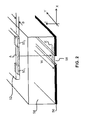
- FIG. 2 illustrates an integrated circuit according to an embodiment.
- the integrated circuit comprise a first 50 1 and second 50 2 electromagnetic radiating elements fabricated on a die 52.
- the die 52 is mounted on the upper surface of a package substrate 54, and the lower surface of the package substrate 54 has a grounding layer 56 provided thereon.
- the package substrate 54 is an electrically insulating substrate formed from high resistivity silicon or GaAs or an insulating substrate formed from a laminate, PTFE, epoxy, etc.
- the grounding layer 56 is adapted to connect to a grounding plane of a PCB.
- the grounding layer 56 comprises a void 58 that is shaped and positioned such that the void 58 is situated directly underneath the area A linearly connecting the first 50 1 and second 50 2 electromagnetic radiating elements.
- the area A connecting the first 50 1 and second 50 2 electromagnetic radiating elements is indicated by a chevron-filled area labelled "A" in Figure 2 .
- this area A connecting the first 50 1 and second 50 2 electromagnetic radiating elements is projected vertically downwards to the grounding layer 56 its horizontal position relative to the grounding layer 56 can be visualised as the area labelled A'.
- the void 58 is positioned underneath the area A linearly connecting the electromagnetic radiating elements 50 1 and 50 2 .
- the void 58 is positioned vertically below the area A filling the horizontal space between the first 50 1 and second 50 2 electromagnetic radiating elements.
- the gap between the first 50 1 and second 50 2 electromagnetic radiating elements there is provided a hole, aperture or gap 58 in the grounding layer 56.
- the horizontal extent of void 58 in the y-axis i.e. the direction in the page of Figure 2
- W is greater than the horizontal extent of the area A in the y-axis, as indicated by the arrow labelled "B”.
- a void 58 may comprise a segment of the grounding layer 56 that has been removed.
- a void may be formed by removing a portion the grounding layer 56. This enables simple formation of the void (by chemical etching or mechanical drilling, for example).
- the embodiment of Figure 2 employs a principle of improving isolation between the first 50 1 and second 50 2 electromagnetic radiating elements by cutting the grounding layer 56 across an electromagnetic field path (represented in a simplified fashion by area A) between the first 50 1 and second 50 2 electromagnetic radiating elements in an attempt to electromagnetically isolate them from each other.
- the void 58 formed in the grounding layer 56 extends across an imaginary path (such as area A) drawn between the first 50 1 and second 50 2 electromagnetic radiating elements.
- Figure 3 shows the variation of isolation versus operating frequency for a conventional circuit (indicated by the dashed line) and for a circuit comprising a ground plane with a void according to an embodiment (indicated by the solid line). From the graph of Figure 3 it can be seen the isolation between radiating elements is improved at microwave frequencies for the circuit according to an embodiment of the invention.
- FIG. 4 there is shown a cross-sectional view of a flip-chip assembly configuration according to an embodiment.
- First 50 1 and second 50 2 electromagnetic radiating elements fabricated on a silicon die 52 (along with other circuit elements 60).
- the die 52 is flip-chip bumped to the upper surface of a package substrate 54 via connecting bumps 62.
- the lower surface of the package substrate 54 has a grounding layer 56 provided thereon.
- the grounding layer 56 is adapted to connect to a grounding plane of a PCB.
- the grounding layer 56 comprises a void 58 that is situated directly underneath the horizontal area (indicated by the arrow labelled "L") extending between the first 50 1 and second 50 2 electromagnetic radiating elements.
- the horizontal width W of the void 58 is less than the horizontal width L of the area extending between the first 50 1 and second 50 2 electromagnetic radiating elements.
- the horizontal width W of the void 58 in this embodiment is 50 ⁇ m.
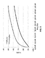
- Figure 5 shows the simulated variation of isolation versus operating frequency for a conventional high-frequency packaged circuit (indicated by the dashed line) and for a high-frequency packaged circuit comprising the embodiment of Figure 4 (indicated by the solid line). From the graph of Figure 5 it can be seen that the embodiment provides a 10dB improvement in isolation when compared to the conventional circuit. Accordingly, embodiments of the invention may help to meet system specifications for a dual polarization receiver operating in microwave frequency bands.
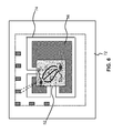
- FIG. 6 and 7 there is shown an embodiment comprising a PCB which may be used in within a package.
- a circuit is fabricated on a die which is flip-chip bonded to a package substrate, wherein the package substrate (and thus also the die) is mounted on a PCB.
- first 50 1 and second 50 2 electromagnetic radiating elements are fabricated on a silicon die 52.
- the die 52 is flip-chip bonded to the upper surface of a package substrate 54 via connecting bumps 62.
- the lower surface of the package substrate 54 has a grounding layer 56 provided thereon.
- the grounding layer 56 comprises a void V that is situated directly underneath the area extending between the first 50 1 and second 50 2 electromagnetic radiating elements.
- the void V extends across an imaginary path Pn drawn between the first 50 1 and second 50 2 electromagnetic radiating elements.
- the package substrate 54 is mounted on the PCB so that the grounding layer is connected to a grounding plane 74 provided on the upper surface of the PCB substrate 72.
- the grounding plane 74 of the PCB 70 also comprises a void V2 which is positioned directly underneath the void V of the grounding layer 56.
- the ground plane may therefore be patterned and this can be used to build other passive functions like an in-package antenna reflector, filters, microwave passive circuits, etc. Accordingly, it will be appreciated that embodiments can be used in satellite communication systems or microwave integrated solutions.
- Embodiments may be used to address isolation requirements in microwave applications, and more particularly satellite communication applications.
- the proposed concept of using a void in the grounding plane so to split the grounding plan between electromagnetic elements may therefore be particularly useful where several receivers need to co-exist in a single die and the isolation requirement between them can be as high as 60dB in the Ku band (12 to 18GHz).
Landscapes
- Semiconductor Integrated Circuits (AREA)
- Shielding Devices Or Components To Electric Or Magnetic Fields (AREA)
- Physics & Mathematics (AREA)
- Health & Medical Sciences (AREA)
- Electromagnetism (AREA)
- Toxicology (AREA)
- Variable-Direction Aerials And Aerial Arrays (AREA)
Abstract
Description
- This invention relates to an integrated circuit, and more particularly to an integrated circuit for packaged device.
- The evolution of radio-communication systems has led to implementations of receiver and/or transmitter chains in integrated circuit form. Well-known examples are used in portable mobile radio frequency (RF) transceiver circuits, satellite communication microwave receivers, WLAN RF circuits etc.
- A schematic block diagram of a typical dual polarization receiver chain in its most elementary form is shown in
Figure 1 . - A
first antenna 10a is for horizontally polarized radiation, and asecond antenna 10b is for vertically polarized radiation. Each antenna includes a electromagnetic radiating element shown as 10a' and 10b', respectively. Each antenna chain has anamplifier filter local oscillator mixer radiating element 16a' and 16b', respectively. - Details of its operation are well known in the field of RF transmitter and receiver circuits. Consequently, detailed explanation of the receiver chain of
Figure 1 will be omitted. - As the two receiver chains are required to operate at the same time, interference and electromagnetic coupling between these two receiver chains should be minimised in order to avoid unwanted inter-modulation signals and achieve optimal operation.
- When provided in integrated circuit form, the circuit contains the oscillators with integrated inductors. Since the inductors and coils are electromagnetic radiating elements, there may be electromagnetic coupling and interference between them. By way of example, the
arrows 20 inFigure 1 represent interference paths. - In order to reduce the coupling between the two receiver chains of an integrated circuit, it is known to employ:
- a large distance on the silicon die to reduce the coupling with the oscillators;
- two separate circuits; and
- flip chip architecture for high frequency applications, as this allows a reduction in electromagnetic coupling by avoiding wire bonds;
- However, the known approaches generally lead to an increase in the circuit area of the integrated circuit and thus requires a larger package.
- Also, as frequency of operation is increased, the isolation is degraded. As a result, the isolation requirements for some high frequency applications, such as satellite communications, cannot easily be met by the known measures. For example, for satellite communications, isolation between the two receiver chains for two polarizations should be at least 60dB at 12GHz.However, the typical isolation performance in conventional packaged circuits is around 45dB at12GHz.
- The invention is defined by the claims.
- There is provided an integrated circuit for a packaged device, the circuit comprising: a circuit having first and second electromagnetic radiating elements fabricated on a die; a package substrate comprising an upper surface and a lower surface; and a grounding layer provided on the lower surface of the package substrate, the grounding layer being adapted to connect to a grounding plane of a printed circuit board (PCB), wherein the die is mounted on the upper surface of the package substrate, and wherein the grounding layer comprises a void, at least a portion of the void being positioned so as to at least partially electromagnetically isolate the first electromagnetic radiating element from the second electromagnetic radiating element.
- At least a portion of the void may be positioned directly below an area extending between the first and second electromagnetic radiating elements. Embodiments may therefore improve electromagnetic isolation between electromagnetic radiating elements by removing a portion of the ground plane positioned underneath and between the electromagnetic radiating elements so that magnetic field generated by one of the radiating elements may be somewhat constrained to the vicinity of the electromagnetic radiating element, thereby reducing electromagnetic coupling to the other radiating element. Embodiments may thus reduce the electromagnetic coupling between two adjacent or neighbouring electromagnetic radiating elements fabricated on a die by having a void formed in the grounding plane of a substrate supporting the die. When viewed from above, the void may be positioned underneath a (footprint) area containing both of the electromagnetic radiating elements.
- Embodiments employ the principle of improving isolation between electromagnetic radiating elements by cutting a ground plane across an electromagnetic field path between the electromagnetic radiating elements in an attempt to electromagnetically isolate the electromagnetic radiating elements from each other. In other words, when viewed from above, the void formed in the ground plane may extend across an imaginary path drawn between the electromagnetic radiating elements.
- Here, the package substrate may be a high resistivity substrate. For the purpose of improved understanding, high resistivity is considered as around 50Ω*cm or above, preferably 100 Ω *cm or above, and even more preferably 1KΩ *cm or above. Conversely, low resistivity is considered to be around or below 10 Ω*cm, preferably below 1Ω*cm, and even more preferably below 1mΩ*cm. Thus, embodiments may employ a high resistivity package substrate having a resistivity that is several orders of magnitude greater than the resistivity of a conventional low resistivity substrate.
- The void may comprise a segment of the grounding layer that has been removed, the segment extending from an edge of the grounding layer. In other words, a void may be formed by removing a portion of an edge of the grounding layer. This enables simple formation of the void. By way of example, a void may be formed by etching or drilling the grounding layer.
- The horizontal extent of the void in a first direction may be greater than that of the area between the first and second electromagnetic radiating elements. This may help to ensure that the electromagnetic field of one electromagnetic radiating is isolated from the other electromagnetic radiating.
- The circuit may comprise a receiver comprising a RF chain having an antenna and a local oscillator, wherein the antenna comprises the first electromagnetic radiating element and the local oscillator comprises the second electromagnetic radiating element. Thus, embodiments may provide a receiver circuit having reduced electromagnetic coupling between electromagnetic radiating elements.
- Existing circuits may be modified according to an embodiment of the invention so as to reduce electromagnetic coupling between adjacent or neighbouring electromagnetic radiating elements fabricated on a die.
- According to another aspect of the invention, there is provided a method of manufacturing an integrated circuit comprising the steps of: providing a circuit having first and second electromagnetic radiating elements fabricated on a die; providing a package substrate comprising an upper surface and a lower surface, a grounding layer being provided on the lower surface of the package substrate and comprising a void, wherein the grounding layer is adapted to connect to a grounding plane of a PCB; and mounting the die on the upper surface of the package substrate such that at least a portion of the void is positioned so as to at least partially electromagnetically isolate the first electromagnetic radiating element from the second electromagnetic radiating element..
- By way of example, embodiments may be employed in a satellite communication receiver or a RF transceiver. Embodiments may be packaged to provide discrete devices. Embodiments may be used in combination with other measures to further reduce electromagnetic coupling and/or interference and achieve required specifications.
- The above and other advantages will be apparent from the exemplary description of the accompanying drawings in which
-
Figure 1 is a schematic block diagram of a typical dual polarization receiver chain in its most elementary form; -
Figure 2 illustrates an integrated circuit according to an embodiment;Figure 3 is a graph illustrating the improvement achieved at microwave frequencies by an embodiment; -
Figure 4 is a cross sectional view of an embodiment; -
Figure 5 is a graph illustrating the improvement in electromagnetic isolation achieved by an embodiment;Figure 6 is a plan view of an embodiment; and -
Figure 7 is a cross sectional view of another embodiment of the invention. - It is proposed to include a void in the grounding layer of a circuit so as to improve isolation between electromagnetic radiating elements.
-
Figure 2 illustrates an integrated circuit according to an embodiment. The integrated circuit comprise a first 501 and second 502 electromagnetic radiating elements fabricated on a die 52. The die 52 is mounted on the upper surface of apackage substrate 54, and the lower surface of thepackage substrate 54 has agrounding layer 56 provided thereon. Here, thepackage substrate 54 is an electrically insulating substrate formed from high resistivity silicon or GaAs or an insulating substrate formed from a laminate, PTFE, epoxy, etc. - The
grounding layer 56 is adapted to connect to a grounding plane of a PCB. - The
grounding layer 56 comprises avoid 58 that is shaped and positioned such that thevoid 58 is situated directly underneath the area A linearly connecting the first 501 and second 502 electromagnetic radiating elements. For a better understanding, the area A connecting the first 501 and second 502 electromagnetic radiating elements is indicated by a chevron-filled area labelled "A" inFigure 2 . When this area A connecting the first 501 and second 502 electromagnetic radiating elements is projected vertically downwards to thegrounding layer 56 its horizontal position relative to thegrounding layer 56 can be visualised as the area labelled A'. Thus, when viewed from vertically above, thevoid 58 is positioned underneath the area A linearly connecting the electromagneticradiating elements - Put another way, the
void 58 is positioned vertically below the area A filling the horizontal space between the first 501 and second 502 electromagnetic radiating elements. Thus, vertically below (when viewed from above) the gap between the first 501 and second 502 electromagnetic radiating elements there is provided a hole, aperture orgap 58 in thegrounding layer 56. Here, the horizontal extent ofvoid 58 in the y-axis (i.e. the direction in the page ofFigure 2 ), as indicated by the arrow labelled "W", is greater than the horizontal extent of the area A in the y-axis, as indicated by the arrow labelled "B". Thus, when expressed as an equation, W>B. - Accordingly, it will be understood that a void 58 may comprise a segment of the
grounding layer 56 that has been removed. In other words, a void may be formed by removing a portion thegrounding layer 56. This enables simple formation of the void (by chemical etching or mechanical drilling, for example). - The embodiment of
Figure 2 employs a principle of improving isolation between the first 501 and second 502 electromagnetic radiating elements by cutting thegrounding layer 56 across an electromagnetic field path (represented in a simplified fashion by area A) between the first 501 and second 502 electromagnetic radiating elements in an attempt to electromagnetically isolate them from each other. In other words, when viewed from above, the void 58 formed in thegrounding layer 56 extends across an imaginary path (such as area A) drawn between the first 501 and second 502 electromagnetic radiating elements. - Such isolation is illustrated by
Figure 3 which shows the variation of isolation versus operating frequency for a conventional circuit (indicated by the dashed line) and for a circuit comprising a ground plane with a void according to an embodiment (indicated by the solid line). From the graph ofFigure 3 it can be seen the isolation between radiating elements is improved at microwave frequencies for the circuit according to an embodiment of the invention. - Experiments may be undertaken using such simulations to optimize the position(s) of a void formed in the grounding layer to minimize electromagnetic coupling between the electromagnetic radiating elements.
- Turning now to
Figure 4 , there is shown a cross-sectional view of a flip-chip assembly configuration according to an embodiment. - First 501 and second 502 electromagnetic radiating elements fabricated on a silicon die 52 (along with other circuit elements 60). The
die 52 is flip-chip bumped to the upper surface of apackage substrate 54 via connecting bumps 62. The lower surface of thepackage substrate 54 has agrounding layer 56 provided thereon. Thegrounding layer 56 is adapted to connect to a grounding plane of a PCB. - The
grounding layer 56 comprises a void 58 that is situated directly underneath the horizontal area (indicated by the arrow labelled "L") extending between the first 501 and second 502 electromagnetic radiating elements. Here, the horizontal width W of the void 58 is less than the horizontal width L of the area extending between the first 501 and second 502 electromagnetic radiating elements. Accordingly, the entire width M of the void 58 situated vertically below the area extending between the first 501 and second 502 electromagnetic radiating elements. By way of example, the horizontal width W of the void 58 in this embodiment is 50µm. -
Figure 5 shows the simulated variation of isolation versus operating frequency for a conventional high-frequency packaged circuit (indicated by the dashed line) and for a high-frequency packaged circuit comprising the embodiment ofFigure 4 (indicated by the solid line). From the graph ofFigure 5 it can be seen that the embodiment provides a 10dB improvement in isolation when compared to the conventional circuit. Accordingly, embodiments of the invention may help to meet system specifications for a dual polarization receiver operating in microwave frequency bands. - Referring now to
Figures 6 and7 there is shown an embodiment comprising a PCB which may be used in within a package. Here, a circuit is fabricated on a die which is flip-chip bonded to a package substrate, wherein the package substrate (and thus also the die) is mounted on a PCB. - In more detail, first 501 and second 502 electromagnetic radiating elements are fabricated on a
silicon die 52. Thedie 52 is flip-chip bonded to the upper surface of apackage substrate 54 via connecting bumps 62. The lower surface of thepackage substrate 54 has agrounding layer 56 provided thereon. - The
grounding layer 56 comprises a void V that is situated directly underneath the area extending between the first 501 and second 502 electromagnetic radiating elements. When viewed from above, as inFigure 6 , the void V extends across an imaginary path Pn drawn between the first 501 and second 502 electromagnetic radiating elements. - The
package substrate 54 is mounted on the PCB so that the grounding layer is connected to agrounding plane 74 provided on the upper surface of thePCB substrate 72. Here, the groundingplane 74 of thePCB 70 also comprises a void V2 which is positioned directly underneath the void V of thegrounding layer 56. - An approach to implementing an embodiment may be summarised in the following steps:
- Identify on the circuit(s) the electromagnetic radiating elements which may be electromagnetically coupled to each other and influence performance;
- employ a flip-chip bumping technique to eliminate bonding wire connexions between circuit pads and package leads. The flip-chip bumping technique may also remove the constraint of the low resistivity of the substrate in case of an integrated circuit on a semi-conductor substrate because, in that case, there is no ground plane directly attached on the semiconductor substrate and therefore there is no degradation of the coupling between the radiating elements; and
- create, in the ground plane, a void to separate the ground plane of each radiating element. Here, the ground plane may be formed from one of the metal layers of the package substrate.
- It may be possible to employ more than one void if there are more than two electromagnetic radiating elements.
- The ground plane may therefore be patterned and this can be used to build other passive functions like an in-package antenna reflector, filters, microwave passive circuits, etc. Accordingly, it will be appreciated that embodiments can be used in satellite communication systems or microwave integrated solutions.
- Embodiments may be used to address isolation requirements in microwave applications, and more particularly satellite communication applications. The proposed concept of using a void in the grounding plane so to split the grounding plan between electromagnetic elements may therefore be particularly useful where several receivers need to co-exist in a single die and the isolation requirement between them can be as high as 60dB in the Ku band (12 to 18GHz).
- Various modifications will be apparent to those skilled in the art. For example, although the above described embodiments comprise a single die, other embodiment may comprise more than one die. Furthermore, although the above described embodiment comprises a single aperture or void vertically below area including both radiating elements, alternative embodiments may employ other arrangements of apertures or void in the grounding plane. By way of example, the embodiment of
Figures 6 and7 may be modified so as to comprise first and second voids in the grounding plane, both voids being substantially parallel and crossing across any imaginary path Pn drawn between the first and second electromagnetic radiating elements.
Claims (15)
- An integrated circuit for a packaged device, the circuit comprising:a circuit having first and second electromagnetic radiating elements fabricated on a die;a package substrate comprising an upper surface and a lower surface; anda grounding layer provided on the lower surface of the package substrate, the grounding layer being adapted to connect to a grounding plane of a printed circuit board, PCB,wherein the die is mounted on the upper surface of the package substrate,and wherein the grounding layer comprises a void, at least a portion of the void being positioned so as to at least partially electromagnetically isolate the first electromagnetic radiating element from the second electromagnetic radiating element.
- The circuit of claim 1, wherein at least a portion of the void is positioned directly below an area extending between the first and second electromagnetic radiating elements.
- The circuit of claim 1 or 2, wherein the void comprises a segment of the grounding layer that has been removed, the segment extending from an edge of the grounding layer.
- The circuit of claim 1, 2 or 3, wherein the package substrate is a high resistivity substrate.
- The circuit of claim 2, wherein the horizontal extent of the void in a first direction is greater than that of the area extending between the first and second electromagnetic radiating elements.
- The circuit of any preceding claim, wherein, when viewed from above, the void extends across an imaginary path drawn between the first and second electromagnetic radiating elements.
- The circuit of any preceding claim, wherein the circuit comprises a receiver comprising a radio frequency chain having an antenna and a local oscillator, and wherein the antenna comprises the first electromagnetic radiating element and the local oscillator comprises the second electromagnetic radiating element.
- The circuit of any preceding claim, wherein the die is flip-chip bumped to the upper surface of the package substrate.
- The circuit of any preceding claims, further comprising a PCB having a grounding plane provided thereon, wherein the package substrate is mounted on the PCB so that the grounding layer is connected to the grounding plane of the PCB.
- The circuit of claim 8, wherein grounding plane of the PCB comprises a void, and wherein at least a portion of the void of the grounding plane is positioned directly below the void of the grounding layer.
- A satellite communication circuit comprising an integrated circuit according to any preceding claim.
- A radio frequency circuit comprising an integrated circuit according to any of claims 1 to 10.
- A packaged device comprising an integrated circuit according to any of claims 1 to 10.
- A method of manufacturing an integrated circuit comprising:providing a circuit having first and second electromagnetic radiating elements fabricated on a die;providing a package substrate comprising an upper surface and a lower surface, a grounding layer being provided on the lower surface of the package substrate and comprising a void, wherein the grounding layer is adapted to connect to a grounding plane of a PCB; andmounting the die on the upper surface of the package substrate such that at least a portion of the void is positioned so as to at least partially electromagnetically isolate the first electromagnetic radiating element from the second electromagnetic radiating element.
- The method of claim 14, further comprising the step of mounting the package substrate on a PCB having a grounding plane so that the grounding layer is connected to the grounding plane of the PCB, wherein the grounding plane of the PCB comprises a void, and wherein at least a portion of the void of the grounding plane is positioned directly below the void of the grounding layer.
Priority Applications (3)
| Application Number | Priority Date | Filing Date | Title |
|---|---|---|---|
| EP14152005.6A EP2860757B1 (en) | 2013-09-11 | 2014-01-21 | Integrated circuit |
| CN201410367999.3A CN104425460B (en) | 2013-09-11 | 2014-07-30 | Integrated circuit |
| US14/479,561 US10403540B2 (en) | 2013-09-11 | 2014-09-08 | Integrated circuit |
Applications Claiming Priority (2)
| Application Number | Priority Date | Filing Date | Title |
|---|---|---|---|
| EP13290215 | 2013-09-11 | ||
| EP14152005.6A EP2860757B1 (en) | 2013-09-11 | 2014-01-21 | Integrated circuit |
Publications (2)
| Publication Number | Publication Date |
|---|---|
| EP2860757A1 true EP2860757A1 (en) | 2015-04-15 |
| EP2860757B1 EP2860757B1 (en) | 2019-12-11 |
Family
ID=52625091
Family Applications (1)
| Application Number | Title | Priority Date | Filing Date |
|---|---|---|---|
| EP14152005.6A Active EP2860757B1 (en) | 2013-09-11 | 2014-01-21 | Integrated circuit |
Country Status (3)
| Country | Link |
|---|---|
| US (1) | US10403540B2 (en) |
| EP (1) | EP2860757B1 (en) |
| CN (1) | CN104425460B (en) |
Families Citing this family (8)
| Publication number | Priority date | Publication date | Assignee | Title |
|---|---|---|---|---|
| EP3159831B1 (en) * | 2015-10-21 | 2018-10-03 | Nxp B.V. | Dual-interface ic card |
| CN106410407A (en) * | 2016-11-30 | 2017-02-15 | 南通沃特光电科技有限公司 | Antenna device having electromagnetic shielding |
| CN106449599A (en) * | 2016-11-30 | 2017-02-22 | 南通沃特光电科技有限公司 | Method for manufacturing antenna device |
| EP3364499B1 (en) * | 2017-02-15 | 2019-11-13 | Nxp B.V. | Antenna |
| US10516207B2 (en) * | 2017-05-17 | 2019-12-24 | Nxp B.V. | High frequency system, communication link |
| WO2019227436A1 (en) * | 2018-05-31 | 2019-12-05 | 华为技术有限公司 | Flip chip package structure and electronic equipment |
| EP3826329B1 (en) * | 2019-11-21 | 2025-01-08 | Oticon A/s | Device with coil |
| SE546798C2 (en) * | 2023-04-27 | 2025-02-18 | Wacqt Ip Ab | Design of a flip-chip assembly for high frequency applications |
Citations (4)
| Publication number | Priority date | Publication date | Assignee | Title |
|---|---|---|---|---|
| EP1251558A2 (en) * | 2001-04-17 | 2002-10-23 | Oki Electric Industry Co., Ltd. | Semiconductor device |
| US20030103006A1 (en) * | 2000-06-30 | 2003-06-05 | Atsushi Yamada | Radio communication device with integrated antenna, transmitter, and receiver |
| US20090130990A1 (en) * | 2006-12-29 | 2009-05-21 | Broadcom Corporation | Multimode transceiver for use with multiple antennas and method for use therewith |
| US20090322643A1 (en) * | 2008-06-30 | 2009-12-31 | Debabani Choudhury | Integrated high performance package systems for mm-wave array applications |
Family Cites Families (12)
| Publication number | Priority date | Publication date | Assignee | Title |
|---|---|---|---|---|
| US6806106B2 (en) * | 2001-03-20 | 2004-10-19 | Infineon Technologies Ag | Bond wire tuning of RF power transistors and amplifiers |
| JP4133747B2 (en) * | 2003-11-07 | 2008-08-13 | 東光株式会社 | Input / output coupling structure of dielectric waveguide |
| US8674888B2 (en) * | 2006-06-21 | 2014-03-18 | Broadcom Corporation | Integrated circuit with power supply line antenna structure and methods for use therewith |
| US20090117855A1 (en) * | 2006-12-29 | 2009-05-07 | Broadcom Corporation | Transceiver for use with multiple antennas and method for use therewith |
| US7979033B2 (en) * | 2006-12-29 | 2011-07-12 | Broadcom Corporation | IC antenna structures and applications thereof |
| US7580001B2 (en) * | 2007-05-25 | 2009-08-25 | Freescale Semiconductor, Inc. | Antenna structure for integrated circuit die using bond wire |
| JP5316305B2 (en) * | 2009-08-13 | 2013-10-16 | ソニー株式会社 | Wireless transmission system and wireless transmission method |
| US8411444B2 (en) * | 2010-09-15 | 2013-04-02 | International Business Machines Corporation | Thermal interface material application for integrated circuit cooling |
| US20120086114A1 (en) * | 2010-10-07 | 2012-04-12 | Broadcom Corporation | Millimeter devices on an integrated circuit |
| US8714459B2 (en) * | 2011-05-12 | 2014-05-06 | Waveconnex, Inc. | Scalable high-bandwidth connectivity |
| JP5788595B2 (en) * | 2011-07-05 | 2015-10-07 | ケッサ・インコーポレーテッド | EHF communication using electrical isolation and dielectric transmission media |
| KR101780024B1 (en) * | 2011-10-19 | 2017-09-20 | 삼성전자주식회사 | Antenna-Printed Circuit Board package |
-
2014
- 2014-01-21 EP EP14152005.6A patent/EP2860757B1/en active Active
- 2014-07-30 CN CN201410367999.3A patent/CN104425460B/en active Active
- 2014-09-08 US US14/479,561 patent/US10403540B2/en active Active
Patent Citations (4)
| Publication number | Priority date | Publication date | Assignee | Title |
|---|---|---|---|---|
| US20030103006A1 (en) * | 2000-06-30 | 2003-06-05 | Atsushi Yamada | Radio communication device with integrated antenna, transmitter, and receiver |
| EP1251558A2 (en) * | 2001-04-17 | 2002-10-23 | Oki Electric Industry Co., Ltd. | Semiconductor device |
| US20090130990A1 (en) * | 2006-12-29 | 2009-05-21 | Broadcom Corporation | Multimode transceiver for use with multiple antennas and method for use therewith |
| US20090322643A1 (en) * | 2008-06-30 | 2009-12-31 | Debabani Choudhury | Integrated high performance package systems for mm-wave array applications |
Also Published As
| Publication number | Publication date |
|---|---|
| CN104425460A (en) | 2015-03-18 |
| CN104425460B (en) | 2017-08-04 |
| US20150070240A1 (en) | 2015-03-12 |
| US10403540B2 (en) | 2019-09-03 |
| EP2860757B1 (en) | 2019-12-11 |
Similar Documents
| Publication | Publication Date | Title |
|---|---|---|
| US10403540B2 (en) | Integrated circuit | |
| CN105190992B (en) | High frequency transmission device | |
| US8994470B2 (en) | Circuit substrate having noise suppression structure | |
| US9666553B2 (en) | Millimeter wave integrated circuit with ball grid array package including transmit and receive channels | |
| US10587044B2 (en) | Flip-chip beamforming integrated circuit with integral thermal mass | |
| CN108233974B (en) | transceiver module | |
| CN104051440B (en) | Semiconductor structure with antenna | |
| US11756902B2 (en) | High-frequency module | |
| JP3734807B2 (en) | Electronic component module | |
| US7586193B2 (en) | Mm-wave antenna using conventional IC packaging | |
| US9468089B2 (en) | EBG structure, semiconductor device, and circuit board | |
| JPWO2020009037A1 (en) | Antenna module and communication device | |
| JP6132692B2 (en) | Antenna device | |
| US20210351518A1 (en) | Low-cost, ipd and laminate based antenna array module | |
| US10797375B2 (en) | Wafer level package with at least one integrated antenna element | |
| JP5132054B2 (en) | On-chip circuit pad structure | |
| EP3850704B1 (en) | Antenna arrays integrated into an electromagnetic transparent metallic surface | |
| EP2493080B1 (en) | High-frequency module and receiver | |
| CN106410407A (en) | Antenna device having electromagnetic shielding | |
| US20180033736A1 (en) | Semiconductor device packages | |
| JP2010272585A (en) | Flip chip mounting structure | |
| EP3429026B1 (en) | An integrated circuit package and method of making thereof | |
| US20110109521A1 (en) | Electronic device comprising a semiconductor component integrating an antenna | |
| US20190341686A1 (en) | High-frequency module and communication device | |
| CN111480225A (en) | semiconductor device |
Legal Events
| Date | Code | Title | Description |
|---|---|---|---|
| PUAI | Public reference made under article 153(3) epc to a published international application that has entered the european phase |
Free format text: ORIGINAL CODE: 0009012 |
|
| 17P | Request for examination filed |
Effective date: 20140326 |
|
| AK | Designated contracting states |
Kind code of ref document: A1 Designated state(s): AL AT BE BG CH CY CZ DE DK EE ES FI FR GB GR HR HU IE IS IT LI LT LU LV MC MK MT NL NO PL PT RO RS SE SI SK SM TR |
|
| AX | Request for extension of the european patent |
Extension state: BA ME |
|
| RBV | Designated contracting states (corrected) |
Designated state(s): AL AT BE BG CH CY CZ DE DK EE ES FI FR GB GR HR HU IE IS IT LI LT LU LV MC MK MT NL NO PL PT RO RS SE SI SK SM TR |
|
| 17Q | First examination report despatched |
Effective date: 20160229 |
|
| GRAP | Despatch of communication of intention to grant a patent |
Free format text: ORIGINAL CODE: EPIDOSNIGR1 |
|
| STAA | Information on the status of an ep patent application or granted ep patent |
Free format text: STATUS: GRANT OF PATENT IS INTENDED |
|
| INTG | Intention to grant announced |
Effective date: 20190729 |
|
| GRAS | Grant fee paid |
Free format text: ORIGINAL CODE: EPIDOSNIGR3 |
|
| GRAA | (expected) grant |
Free format text: ORIGINAL CODE: 0009210 |
|
| STAA | Information on the status of an ep patent application or granted ep patent |
Free format text: STATUS: THE PATENT HAS BEEN GRANTED |
|
| AK | Designated contracting states |
Kind code of ref document: B1 Designated state(s): AL AT BE BG CH CY CZ DE DK EE ES FI FR GB GR HR HU IE IS IT LI LT LU LV MC MK MT NL NO PL PT RO RS SE SI SK SM TR |
|
| REG | Reference to a national code |
Ref country code: GB Ref legal event code: FG4D |
|
| REG | Reference to a national code |
Ref country code: CH Ref legal event code: EP |
|
| REG | Reference to a national code |
Ref country code: AT Ref legal event code: REF Ref document number: 1213046 Country of ref document: AT Kind code of ref document: T Effective date: 20191215 |
|
| REG | Reference to a national code |
Ref country code: DE Ref legal event code: R096 Ref document number: 602014058129 Country of ref document: DE |
|
| REG | Reference to a national code |
Ref country code: IE Ref legal event code: FG4D |
|
| REG | Reference to a national code |
Ref country code: NL Ref legal event code: MP Effective date: 20191211 |
|
| REG | Reference to a national code |
Ref country code: LT Ref legal event code: MG4D |
|
| PG25 | Lapsed in a contracting state [announced via postgrant information from national office to epo] |
Ref country code: NO Free format text: LAPSE BECAUSE OF FAILURE TO SUBMIT A TRANSLATION OF THE DESCRIPTION OR TO PAY THE FEE WITHIN THE PRESCRIBED TIME-LIMIT Effective date: 20200311 Ref country code: FI Free format text: LAPSE BECAUSE OF FAILURE TO SUBMIT A TRANSLATION OF THE DESCRIPTION OR TO PAY THE FEE WITHIN THE PRESCRIBED TIME-LIMIT Effective date: 20191211 Ref country code: BG Free format text: LAPSE BECAUSE OF FAILURE TO SUBMIT A TRANSLATION OF THE DESCRIPTION OR TO PAY THE FEE WITHIN THE PRESCRIBED TIME-LIMIT Effective date: 20200311 Ref country code: GR Free format text: LAPSE BECAUSE OF FAILURE TO SUBMIT A TRANSLATION OF THE DESCRIPTION OR TO PAY THE FEE WITHIN THE PRESCRIBED TIME-LIMIT Effective date: 20200312 Ref country code: LT Free format text: LAPSE BECAUSE OF FAILURE TO SUBMIT A TRANSLATION OF THE DESCRIPTION OR TO PAY THE FEE WITHIN THE PRESCRIBED TIME-LIMIT Effective date: 20191211 Ref country code: SE Free format text: LAPSE BECAUSE OF FAILURE TO SUBMIT A TRANSLATION OF THE DESCRIPTION OR TO PAY THE FEE WITHIN THE PRESCRIBED TIME-LIMIT Effective date: 20191211 Ref country code: LV Free format text: LAPSE BECAUSE OF FAILURE TO SUBMIT A TRANSLATION OF THE DESCRIPTION OR TO PAY THE FEE WITHIN THE PRESCRIBED TIME-LIMIT Effective date: 20191211 Ref country code: ES Free format text: LAPSE BECAUSE OF FAILURE TO SUBMIT A TRANSLATION OF THE DESCRIPTION OR TO PAY THE FEE WITHIN THE PRESCRIBED TIME-LIMIT Effective date: 20191211 |
|
| PG25 | Lapsed in a contracting state [announced via postgrant information from national office to epo] |
Ref country code: HR Free format text: LAPSE BECAUSE OF FAILURE TO SUBMIT A TRANSLATION OF THE DESCRIPTION OR TO PAY THE FEE WITHIN THE PRESCRIBED TIME-LIMIT Effective date: 20191211 Ref country code: RS Free format text: LAPSE BECAUSE OF FAILURE TO SUBMIT A TRANSLATION OF THE DESCRIPTION OR TO PAY THE FEE WITHIN THE PRESCRIBED TIME-LIMIT Effective date: 20191211 |
|
| PG25 | Lapsed in a contracting state [announced via postgrant information from national office to epo] |
Ref country code: AL Free format text: LAPSE BECAUSE OF FAILURE TO SUBMIT A TRANSLATION OF THE DESCRIPTION OR TO PAY THE FEE WITHIN THE PRESCRIBED TIME-LIMIT Effective date: 20191211 |
|
| PG25 | Lapsed in a contracting state [announced via postgrant information from national office to epo] |
Ref country code: CZ Free format text: LAPSE BECAUSE OF FAILURE TO SUBMIT A TRANSLATION OF THE DESCRIPTION OR TO PAY THE FEE WITHIN THE PRESCRIBED TIME-LIMIT Effective date: 20191211 Ref country code: NL Free format text: LAPSE BECAUSE OF FAILURE TO SUBMIT A TRANSLATION OF THE DESCRIPTION OR TO PAY THE FEE WITHIN THE PRESCRIBED TIME-LIMIT Effective date: 20191211 Ref country code: RO Free format text: LAPSE BECAUSE OF FAILURE TO SUBMIT A TRANSLATION OF THE DESCRIPTION OR TO PAY THE FEE WITHIN THE PRESCRIBED TIME-LIMIT Effective date: 20191211 Ref country code: PT Free format text: LAPSE BECAUSE OF FAILURE TO SUBMIT A TRANSLATION OF THE DESCRIPTION OR TO PAY THE FEE WITHIN THE PRESCRIBED TIME-LIMIT Effective date: 20200506 Ref country code: EE Free format text: LAPSE BECAUSE OF FAILURE TO SUBMIT A TRANSLATION OF THE DESCRIPTION OR TO PAY THE FEE WITHIN THE PRESCRIBED TIME-LIMIT Effective date: 20191211 |
|
| PG25 | Lapsed in a contracting state [announced via postgrant information from national office to epo] |
Ref country code: IS Free format text: LAPSE BECAUSE OF FAILURE TO SUBMIT A TRANSLATION OF THE DESCRIPTION OR TO PAY THE FEE WITHIN THE PRESCRIBED TIME-LIMIT Effective date: 20200411 Ref country code: SM Free format text: LAPSE BECAUSE OF FAILURE TO SUBMIT A TRANSLATION OF THE DESCRIPTION OR TO PAY THE FEE WITHIN THE PRESCRIBED TIME-LIMIT Effective date: 20191211 Ref country code: SK Free format text: LAPSE BECAUSE OF FAILURE TO SUBMIT A TRANSLATION OF THE DESCRIPTION OR TO PAY THE FEE WITHIN THE PRESCRIBED TIME-LIMIT Effective date: 20191211 |
|
| REG | Reference to a national code |
Ref country code: CH Ref legal event code: PL |
|
| REG | Reference to a national code |
Ref country code: DE Ref legal event code: R097 Ref document number: 602014058129 Country of ref document: DE |
|
| PG25 | Lapsed in a contracting state [announced via postgrant information from national office to epo] |
Ref country code: MC Free format text: LAPSE BECAUSE OF FAILURE TO SUBMIT A TRANSLATION OF THE DESCRIPTION OR TO PAY THE FEE WITHIN THE PRESCRIBED TIME-LIMIT Effective date: 20191211 |
|
| REG | Reference to a national code |
Ref country code: BE Ref legal event code: MM Effective date: 20200131 Ref country code: AT Ref legal event code: MK05 Ref document number: 1213046 Country of ref document: AT Kind code of ref document: T Effective date: 20191211 |
|
| PLBE | No opposition filed within time limit |
Free format text: ORIGINAL CODE: 0009261 |
|
| STAA | Information on the status of an ep patent application or granted ep patent |
Free format text: STATUS: NO OPPOSITION FILED WITHIN TIME LIMIT |
|
| PG25 | Lapsed in a contracting state [announced via postgrant information from national office to epo] |
Ref country code: LU Free format text: LAPSE BECAUSE OF NON-PAYMENT OF DUE FEES Effective date: 20200121 Ref country code: DK Free format text: LAPSE BECAUSE OF FAILURE TO SUBMIT A TRANSLATION OF THE DESCRIPTION OR TO PAY THE FEE WITHIN THE PRESCRIBED TIME-LIMIT Effective date: 20191211 |
|
| 26N | No opposition filed |
Effective date: 20200914 |
|
| PG25 | Lapsed in a contracting state [announced via postgrant information from national office to epo] |
Ref country code: AT Free format text: LAPSE BECAUSE OF FAILURE TO SUBMIT A TRANSLATION OF THE DESCRIPTION OR TO PAY THE FEE WITHIN THE PRESCRIBED TIME-LIMIT Effective date: 20191211 Ref country code: BE Free format text: LAPSE BECAUSE OF NON-PAYMENT OF DUE FEES Effective date: 20200131 Ref country code: PL Free format text: LAPSE BECAUSE OF FAILURE TO SUBMIT A TRANSLATION OF THE DESCRIPTION OR TO PAY THE FEE WITHIN THE PRESCRIBED TIME-LIMIT Effective date: 20191211 Ref country code: LI Free format text: LAPSE BECAUSE OF NON-PAYMENT OF DUE FEES Effective date: 20200131 Ref country code: CH Free format text: LAPSE BECAUSE OF NON-PAYMENT OF DUE FEES Effective date: 20200131 Ref country code: SI Free format text: LAPSE BECAUSE OF FAILURE TO SUBMIT A TRANSLATION OF THE DESCRIPTION OR TO PAY THE FEE WITHIN THE PRESCRIBED TIME-LIMIT Effective date: 20191211 |
|
| PG25 | Lapsed in a contracting state [announced via postgrant information from national office to epo] |
Ref country code: IT Free format text: LAPSE BECAUSE OF FAILURE TO SUBMIT A TRANSLATION OF THE DESCRIPTION OR TO PAY THE FEE WITHIN THE PRESCRIBED TIME-LIMIT Effective date: 20191211 Ref country code: IE Free format text: LAPSE BECAUSE OF NON-PAYMENT OF DUE FEES Effective date: 20200121 |
|
| GBPC | Gb: european patent ceased through non-payment of renewal fee |
Effective date: 20200311 |
|
| PG25 | Lapsed in a contracting state [announced via postgrant information from national office to epo] |
Ref country code: GB Free format text: LAPSE BECAUSE OF NON-PAYMENT OF DUE FEES Effective date: 20200311 |
|
| PG25 | Lapsed in a contracting state [announced via postgrant information from national office to epo] |
Ref country code: TR Free format text: LAPSE BECAUSE OF FAILURE TO SUBMIT A TRANSLATION OF THE DESCRIPTION OR TO PAY THE FEE WITHIN THE PRESCRIBED TIME-LIMIT Effective date: 20191211 Ref country code: MT Free format text: LAPSE BECAUSE OF FAILURE TO SUBMIT A TRANSLATION OF THE DESCRIPTION OR TO PAY THE FEE WITHIN THE PRESCRIBED TIME-LIMIT Effective date: 20191211 Ref country code: CY Free format text: LAPSE BECAUSE OF FAILURE TO SUBMIT A TRANSLATION OF THE DESCRIPTION OR TO PAY THE FEE WITHIN THE PRESCRIBED TIME-LIMIT Effective date: 20191211 |
|
| PG25 | Lapsed in a contracting state [announced via postgrant information from national office to epo] |
Ref country code: MK Free format text: LAPSE BECAUSE OF FAILURE TO SUBMIT A TRANSLATION OF THE DESCRIPTION OR TO PAY THE FEE WITHIN THE PRESCRIBED TIME-LIMIT Effective date: 20191211 |
|
| P01 | Opt-out of the competence of the unified patent court (upc) registered |
Effective date: 20230725 |
|
| REG | Reference to a national code |
Ref country code: DE Ref legal event code: R079 Ref document number: 602014058129 Country of ref document: DE Free format text: PREVIOUS MAIN CLASS: H01L0023552000 Ipc: H10W0042200000 |
|
| PGFP | Annual fee paid to national office [announced via postgrant information from national office to epo] |
Ref country code: FR Payment date: 20251217 Year of fee payment: 13 |
|
| PGFP | Annual fee paid to national office [announced via postgrant information from national office to epo] |
Ref country code: DE Payment date: 20251217 Year of fee payment: 13 |