EP2859402B1 - Directional backlight with a modulation layer - Google Patents
Directional backlight with a modulation layer Download PDFInfo
- Publication number
- EP2859402B1 EP2859402B1 EP12877856.0A EP12877856A EP2859402B1 EP 2859402 B1 EP2859402 B1 EP 2859402B1 EP 12877856 A EP12877856 A EP 12877856A EP 2859402 B1 EP2859402 B1 EP 2859402B1
- Authority
- EP
- European Patent Office
- Prior art keywords
- directional
- pixels
- lightbeams
- backlight
- backplane
- Prior art date
- Legal status (The legal status is an assumption and is not a legal conclusion. Google has not performed a legal analysis and makes no representation as to the accuracy of the status listed.)
- Active
Links
- 238000000034 method Methods 0.000 claims description 11
- 239000012780 transparent material Substances 0.000 claims description 5
- 125000006850 spacer group Chemical group 0.000 claims description 4
- 238000003079 width control Methods 0.000 claims 1
- 239000000463 material Substances 0.000 description 7
- 239000011521 glass Substances 0.000 description 4
- 239000003989 dielectric material Substances 0.000 description 3
- 229910052751 metal Inorganic materials 0.000 description 3
- 239000002184 metal Substances 0.000 description 3
- 239000003086 colorant Substances 0.000 description 2
- 238000010586 diagram Methods 0.000 description 2
- 239000004033 plastic Substances 0.000 description 2
- 230000001902 propagating effect Effects 0.000 description 2
- 239000010453 quartz Substances 0.000 description 2
- VYPSYNLAJGMNEJ-UHFFFAOYSA-N silicon dioxide Inorganic materials O=[Si]=O VYPSYNLAJGMNEJ-UHFFFAOYSA-N 0.000 description 2
- 229910052581 Si3N4 Inorganic materials 0.000 description 1
- 230000004888 barrier function Effects 0.000 description 1
- 230000015572 biosynthetic process Effects 0.000 description 1
- 238000010168 coupling process Methods 0.000 description 1
- 238000005859 coupling reaction Methods 0.000 description 1
- 230000000694 effects Effects 0.000 description 1
- 238000004049 embossing Methods 0.000 description 1
- 238000005516 engineering process Methods 0.000 description 1
- 238000005286 illumination Methods 0.000 description 1
- 238000003384 imaging method Methods 0.000 description 1
- AMGQUBHHOARCQH-UHFFFAOYSA-N indium;oxotin Chemical compound [In].[Sn]=O AMGQUBHHOARCQH-UHFFFAOYSA-N 0.000 description 1
- 239000004973 liquid crystal related substance Substances 0.000 description 1
- 238000001459 lithography Methods 0.000 description 1
- 238000004519 manufacturing process Methods 0.000 description 1
- 238000012986 modification Methods 0.000 description 1
- 230000004048 modification Effects 0.000 description 1
- 238000001127 nanoimprint lithography Methods 0.000 description 1
- 238000009304 pastoral farming Methods 0.000 description 1
- 238000000206 photolithography Methods 0.000 description 1
- HQVNEWCFYHHQES-UHFFFAOYSA-N silicon nitride Chemical compound N12[Si]34N5[Si]62N3[Si]51N64 HQVNEWCFYHHQES-UHFFFAOYSA-N 0.000 description 1
- 230000003595 spectral effect Effects 0.000 description 1
Images


Classifications
-
- G—PHYSICS
- G02—OPTICS
- G02B—OPTICAL ELEMENTS, SYSTEMS OR APPARATUS
- G02B6/00—Light guides; Structural details of arrangements comprising light guides and other optical elements, e.g. couplings
- G02B6/0001—Light guides; Structural details of arrangements comprising light guides and other optical elements, e.g. couplings specially adapted for lighting devices or systems
- G02B6/0011—Light guides; Structural details of arrangements comprising light guides and other optical elements, e.g. couplings specially adapted for lighting devices or systems the light guides being planar or of plate-like form
- G02B6/0033—Means for improving the coupling-out of light from the light guide
- G02B6/0035—Means for improving the coupling-out of light from the light guide provided on the surface of the light guide or in the bulk of it
- G02B6/004—Scattering dots or dot-like elements, e.g. microbeads, scattering particles, nanoparticles
- G02B6/0043—Scattering dots or dot-like elements, e.g. microbeads, scattering particles, nanoparticles provided on the surface of the light guide
-
- G—PHYSICS
- G02—OPTICS
- G02B—OPTICAL ELEMENTS, SYSTEMS OR APPARATUS
- G02B27/00—Optical systems or apparatus not provided for by any of the groups G02B1/00 - G02B26/00, G02B30/00
- G02B27/10—Beam splitting or combining systems
- G02B27/1086—Beam splitting or combining systems operating by diffraction only
-
- G—PHYSICS
- G02—OPTICS
- G02B—OPTICAL ELEMENTS, SYSTEMS OR APPARATUS
- G02B30/00—Optical systems or apparatus for producing three-dimensional [3D] effects, e.g. stereoscopic images
- G02B30/20—Optical systems or apparatus for producing three-dimensional [3D] effects, e.g. stereoscopic images by providing first and second parallax images to an observer's left and right eyes
- G02B30/26—Optical systems or apparatus for producing three-dimensional [3D] effects, e.g. stereoscopic images by providing first and second parallax images to an observer's left and right eyes of the autostereoscopic type
- G02B30/33—Optical systems or apparatus for producing three-dimensional [3D] effects, e.g. stereoscopic images by providing first and second parallax images to an observer's left and right eyes of the autostereoscopic type involving directional light or back-light sources
-
- G—PHYSICS
- G02—OPTICS
- G02B—OPTICAL ELEMENTS, SYSTEMS OR APPARATUS
- G02B6/00—Light guides; Structural details of arrangements comprising light guides and other optical elements, e.g. couplings
- G02B6/0001—Light guides; Structural details of arrangements comprising light guides and other optical elements, e.g. couplings specially adapted for lighting devices or systems
- G02B6/0011—Light guides; Structural details of arrangements comprising light guides and other optical elements, e.g. couplings specially adapted for lighting devices or systems the light guides being planar or of plate-like form
- G02B6/0033—Means for improving the coupling-out of light from the light guide
- G02B6/0035—Means for improving the coupling-out of light from the light guide provided on the surface of the light guide or in the bulk of it
- G02B6/0036—2-D arrangement of prisms, protrusions, indentations or roughened surfaces
-
- G—PHYSICS
- G02—OPTICS
- G02B—OPTICAL ELEMENTS, SYSTEMS OR APPARATUS
- G02B6/00—Light guides; Structural details of arrangements comprising light guides and other optical elements, e.g. couplings
- G02B6/0001—Light guides; Structural details of arrangements comprising light guides and other optical elements, e.g. couplings specially adapted for lighting devices or systems
- G02B6/0011—Light guides; Structural details of arrangements comprising light guides and other optical elements, e.g. couplings specially adapted for lighting devices or systems the light guides being planar or of plate-like form
- G02B6/0033—Means for improving the coupling-out of light from the light guide
- G02B6/0058—Means for improving the coupling-out of light from the light guide varying in density, size, shape or depth along the light guide
-
- G—PHYSICS
- G02—OPTICS
- G02B—OPTICAL ELEMENTS, SYSTEMS OR APPARATUS
- G02B6/00—Light guides; Structural details of arrangements comprising light guides and other optical elements, e.g. couplings
- G02B6/0001—Light guides; Structural details of arrangements comprising light guides and other optical elements, e.g. couplings specially adapted for lighting devices or systems
- G02B6/0011—Light guides; Structural details of arrangements comprising light guides and other optical elements, e.g. couplings specially adapted for lighting devices or systems the light guides being planar or of plate-like form
- G02B6/0066—Light guides; Structural details of arrangements comprising light guides and other optical elements, e.g. couplings specially adapted for lighting devices or systems the light guides being planar or of plate-like form characterised by the light source being coupled to the light guide
- G02B6/0068—Arrangements of plural sources, e.g. multi-colour light sources
-
- G—PHYSICS
- G02—OPTICS
- G02B—OPTICAL ELEMENTS, SYSTEMS OR APPARATUS
- G02B6/00—Light guides; Structural details of arrangements comprising light guides and other optical elements, e.g. couplings
- G02B6/0001—Light guides; Structural details of arrangements comprising light guides and other optical elements, e.g. couplings specially adapted for lighting devices or systems
- G02B6/0011—Light guides; Structural details of arrangements comprising light guides and other optical elements, e.g. couplings specially adapted for lighting devices or systems the light guides being planar or of plate-like form
- G02B6/0075—Arrangements of multiple light guides
- G02B6/0078—Side-by-side arrangements, e.g. for large area displays
-
- H—ELECTRICITY
- H04—ELECTRIC COMMUNICATION TECHNIQUE
- H04N—PICTORIAL COMMUNICATION, e.g. TELEVISION
- H04N13/00—Stereoscopic video systems; Multi-view video systems; Details thereof
- H04N13/30—Image reproducers
- H04N13/302—Image reproducers for viewing without the aid of special glasses, i.e. using autostereoscopic displays
- H04N13/32—Image reproducers for viewing without the aid of special glasses, i.e. using autostereoscopic displays using arrays of controllable light sources; using moving apertures or moving light sources
Definitions
- US2010/207964A1 describes a display device with an integrated backlight layer structure utilizing separate color diffractive out-couplings.
- a light field is the set of all light rays traveling in every direction through every point in space. Any natural, real-world scene can be fully characterized by its light field, providing information on the intensity, color, and direction of all light rays passing through the scene. The goal is to enable viewers of a display screen to experience a scene as one would experience it in person.
- 3D displays have recently emerged but suffer from inefficiencies in angular and spatial resolution in addition to providing a limited number of views. Examples include 3D displays based on holograms, parallax barriers, or lenticular lenses.
- a common theme among these displays is their difficulty to generate light fields that are controlled with precision at the pixel level to achieve good image quality for a wide range of viewing angles and spatial resolutions.
- a directional backlight with a modulation layer is disclosed.
- a directional backlight is a layer in a display screen (e.g., an LCD display screen) that is used to provide a light field in the form of directional lightbeams.
- the directional lightbeams are scattered by a plurality of directional pixels in the directional backlight.
- Each directional lightbeam originates from a different directional pixel and has a given direction and angular spread based on characteristics of the directional pixel. This pointed directionality enables directional beams to be modulated (i.e., turned on, off or changed in brightness) using a plurality of modulators.
- the modulators may be, for example, Liquid Crystal Display (“LCD”) cells (with or without polarizers).
- LCD Liquid Crystal Display
- Other types of modulators may be used, such as those based on a different mechanism including micro-electrical-mechanical (“MEMS”), fluidic, magnetic, electrophoretic, or other mechanism that modulates the intensity of light upon application of an electrical signal.
- MEMS micro-electrical-mechanical
- the directional pixels are arranged in a directional backplane that is illuminated by a plurality of input planar lightbeams.
- the directional pixels receive the input planar lightbeams and scatter a fraction of them into directional lightbeams.
- a modulation layer is placed above the directional pixels to modulate the directional lightbeams as desired.
- the modulation layer includes a plurality of modulators (e.g., LCD cells), with each modulator modulating a single directional lightbeam from a single directional pixel or a set of directional lightbeams from a set of directional pixels.
- the modulation layer enables 3D images to be generated with many different views, with each view provided by a set of directional lightbeams.
- the directional pixels in the directional backplane have patterned gratings of substantially parallel grooves arranged in or on top of the directional backplane.
- the directional backplane may be, for example, a slab of transparent material that guides the input planar lightbeams into the directional pixels, such as, for example, Silicon Nitride ("SiN"), glass or quartz, plastic, Indium Tin Oxide ("ITO”), among others.
- the patterned gratings can consist of grooves etched directly in or made of material deposited on top of the directional backplane or the waveguides (e.g., any material that can be deposited and etched or lift-off, including any dielectrics or metal).
- the grooves may also be slanted.
- each directional pixel may be specified by a grating length (i.e., dimension along the propagation axis of the input planar lightbeams), a grating width (i.e., dimension across the propagation axis of the input planar lightbeams), a groove orientation, a pitch, and a duty cycle.
- Each directional pixel may emit a directional lightbeam with a direction that is determined by the groove orientation and the grating pitch and with an angular spread that is determined by the grating length and width.
- the second Fourier coefficient of the patterned gratings vanishes thereby preventing the scattering of light in additional unwanted directions. This insures that only one directional lightbeam emerges from each directional pixel regardless of its output angle.
- a directional backlight can be designed with directional pixels that have a certain grating length, a grating width, a groove orientation, a pitch and a duty cycle that are selected to produce a given 3D image.
- the 3D image is generated from the directional lightbeams emitted by the directional pixels and modulated by the modulation layer, with modulated directional lightbeams from a set of directional pixels generating a given image view.
- Directional backlight 100 includes a directional backplane 105 that receives a set of input planar lightbeams 110 from a plurality of light sources.
- the plurality of light sources may include, for example, one or more narrow-bandwidth light sources with a spectral bandwidth of approximately 30 nm or less, such as Light Emitting Diodes ("LEDs"), lasers, and so on.
- the input planar lightbeams 110 propagate in substantially the same plane as the directional backplane 105, which is designed to be substantially planar.
- the directional backplane 105 may consist of a slab of a transparent material (e.g., SiN, glass or quartz, plastic, ITO, etc.) having a plurality of directional pixels 115a-d arranged in or on top of the directional backplane 105.
- the directional pixels 115a-d scatter a fraction of the input planar lightbeams 110 into directional lightbeams 120a-d.
- each directional pixel 115a-d has patterned gratings of substantially parallel grooves, e.g., grooves 125a for directional pixel 115a.
- the thickness of the grating grooves can be substantially the same for all grooves resulting in a substantially planar design.
- the grooves can be etched in the directional backplane or be made of material deposited on top of the directional backplane 105 (e.g., any material that can be deposited and etched or lift-off, including any dielectrics or metal).
- Each directional lightbeam 120a-d has a given direction and an angular spread that is determined by the patterned grating forming the corresponding directional pixel 115a-d.
- the direction of each directional lightbeam 120a-d is determined by the orientation and the grating pitch of the patterned gratings.
- the angular spread of each directional lightbeam is in turn determined by the grating length and width of the patterned gratings.
- the direction of directional lightbeam 115a is determined by the orientation and the grating pitch of patterned gratings 125a.
- this substantially planar design and the formation of directional lightbeams 120a-d from input planar lightbeams 110 requires gratings having a substantially smaller pitch than traditional diffraction gratings.
- traditional diffraction gratings scatter light upon illumination with lightbeams that are propagating substantially across the plane of the grating.
- the gratings in each directional pixel 115a-d are substantially on the same plane as the input planar lightbeams 110 when generating the directional lightbeams 120a-d.
- the directional lightbeams 120a-d are precisely controlled by characteristics of the gratings in directional pixels 115a-d including a grating length L, a grating width W, a groove orientation ⁇ , and a grating pitch ⁇ .
- the grating length L of grating 125a controls the angular spread ⁇ of the directional lightbeam 120a along the input light propagation axis
- the grating width W controls the angular spread ⁇ of the directional lightbeam 120a across the input light propagation axis, as follows: ⁇ ⁇ 4 ⁇ ⁇ L 4 ⁇ ⁇ W where ⁇ is the wavelength of the directional lightbeam 120a.
- the groove orientation, specified by the grating orientation angle ⁇ , and the grating pitch or period, specified by ⁇ control the direction of the directional lightbeam 120a.
- the grating length L and the grating width W can vary in size in the range of 0.1 to 200 ⁇ m.
- the groove orientation angle ⁇ and the grating pitch ⁇ may be set to satisfy a desired direction of the directional lightbeam 120a, with, for example, the groove orientation angle ⁇ on the order of -40 to +40 degrees and the grating pitch ⁇ on the order of 200-700 nm.
- a modulation layer 130 having a plurality of modulators is positioned above the directional pixels 115a-d to modulate the directional lightbeams 120a-d scattered by the directional pixels 115a-d.
- Modulation of directional lightbeams 120a-d involves controlling their brightness with the modulators (e.g., turning them on, off, or changing their brightness).
- the modulators in the modulation layer 130 may be used to turn on directional lightbeams 120a and 120d and turn off directional lightbeams 120b and 120c.
- the ability to provide modulation for the directional lightbeams 120a-d enables many different image views to be generated.
- the modulation layer 130 may be placed on top of a spacer layer 135, which may be made of a material or simply consist of a spacing (i.e., air) between the directional pixels 115a-d and the modulators the modulation layer 130.
- the spacer layer 135 may have a width, for example, on the order of 0-100 ⁇ m.
- directional backplane 105 is shown with four directional pixels 115a-d for illustration purposes only.
- a directional backplane in accordance with various examples can be designed with many directional pixels (e.g., higher than 100), depending on how the directional backplane is used (e.g., in a 3D display screen, in a 3D watch, in a mobile device, etc.).
- the directional pixels may have any shape, including for example, a circle, an ellipse, a polygon, or other geometrical shape.
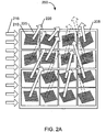
- FIGS. 2A-B illustrate top views of a directional backlight according to FIG. 1 .
- directional backlight 200 is show with a directional backplane 205 consisting of a plurality of polygonal directional pixels (e.g., directional pixel 210) arranged in a transparent slab. Each directional pixel is able to scatter a portion of the input planar lightbeams 215 into an output directional lightbeam (e.g., directional lightbeam 220). Each directional lightbeam is modulated by a modulator, e.g., LCD cell 225 for directional lightbeam 220.
- the directional lightbeams scattered by all the directional pixels in the directional backplane 205 and modulated by the modulators e.g., LCD cell 225
- directional backlight 230 is show with a directional backplane 235 consisting of a plurality of circular directional pixels (e.g., directional pixel 240) arranged in a transparent slab. Each directional pixel is able to scatter a portion of the input planar lightbeams 245 into an output directional lightbeam (e.g., directional lightbeam 250). Each directional lightbeam is modulated by a modulator, e.g., LCD cell 255 for directional lightbeam 250.
- the directional lightbeams scattered by all the directional pixels in the directional backplane 235 and modulated by the modulators e.g., LCD cell 255) can represent multiple image views that when combined form a 3D image.
- a single modulator may be used to modulate a set of directional lightbeams from a set of directional pixels. That is, a given modulator may be placed above a set of directional pixels instead of having a single modulator per directional pixel as shown in FIGS. 2A-B .
- directional backlight 300 is show with a directional backplane 305 consisting of a plurality of polygonal directional pixels (e.g., directional pixel 310a) arranged in a transparent slab. Each directional pixel is able to scatter a portion of the input planar lightbeams 315 into an output directional lightbeam (e.g., directional lightbeam 320a).
- a directional backplane 305 consisting of a plurality of polygonal directional pixels (e.g., directional pixel 310a) arranged in a transparent slab.
- Each directional pixel is able to scatter a portion of the input planar lightbeams 315 into an output directional lightbeam (e.g., directional lightbeam 320a).
- a set of directional lightbeams (e.g., directional lightbeams 320a-d scattered by directional pixels 310a-d) is modulated by a modulator (e.g., LCD cell 325a to modulate directional lightbeams 320a-d).
- a modulator e.g., LCD cell 325a to modulate directional lightbeams 320a-d.
- LCD cell 325a is used to turn on directional pixels 310a-d while LCD cell 325d is used to turn off directional pixels 330a-d.
- the directional lightbeams scattered by all the directional pixels in the directional backplane 305 and modulated by the LCD cells 325a-d can represent multiple image views that when combined form a 3D image.
- directional backlight 340 is show with a directional backplane 345 consisting of a plurality of circular directional pixels (e.g., directional pixel 350a) arranged in a transparent slab. Each directional pixel is able to scatter a portion of the input planar lightbeams 355 into an output directional lightbeam (e.g., directional lightbeam 360a).
- a set of directional lightbeams e.g., directional lightbeams 360a-d scattered by directional pixels 350a-d
- a modulator e.g., LCD cell 370a to modulate directional lightbeams 360a-d.
- LCD cell 370a is used to turn on directional pixels 350a-d while LCD cell 370d is used to turn off directional pixels 365a-d.
- the directional lightbeams scattered by all the directional pixels in the directional backplane 345 and modulated by modulators such as the LCD cells 370a-d can represent multiple image views that when combined form a 3D image.
- a directional backplane may be designed to have different shapes, such as, for example, a triangular shape (as shown in FIG. 4 ), a hexagonal shape (as shown in FIG. 5 ), or a circular shape (as shown in FIG. 6 ).
- the directional backplane 405 receives input planar lightbeams from three different spatial directions, e.g., input planar lightbeams 410-420.
- This configuration may be used when the input planar lightbeams represent light of different colors, e.g., with input planar lightbeams 410 representing a red color, input planar lightbeams 415 representing a green color, and input planar lightbeams 420 representing a blue color.
- Each of the input planar lightbeams 410-420 is disposed on a side of the triangular directional backplane 405 to focus their light on a set of directional pixels.
- the input planar lightbeams 410 is scattered into directional lightbeams by a set of directional pixels 425-435.
- This subset of directional pixels 425-435 may also receive light from the input planar lightbeams 415-420. However, by design this light is not scattered in the intended view zone of the directional backlight 400.
- planar lightbeams 410 are scattered by a subset G A of directional pixels 425-435 into an intended view zone.
- the intended view zone may be specified by a maximum ray angle ⁇ max measured from a normal to the directional backlight 400.
- Input planar lightbeams 410 may also be scattered by a subset of directional pixels G B 440-450, however those unwanted rays are outside the intended view zone as long as: sin ⁇ max ⁇ ⁇ A + ⁇ B ⁇ A ⁇ B n eff A ⁇ A 2 + n eff B ⁇ B 2 ⁇ n eff A ⁇ A n eff B ⁇ B
- ⁇ A is the wavelength of input planar lightbeams 410
- n eff A is the effective index of horizontal propagation of input planar lightbeams 410 in the directional backplane 405
- ⁇ B is the wavelength of input planar lightbeams 420 (to be scattered by directional pixels 440-450)
- n eff B is the effective index of horizontal propagation of input planar lightbeams 420 in the directional backplane 405.
- Equation 2 reduces to: sin ⁇ max ⁇ n eff 2
- n eff ⁇ 2 and sin ⁇ max ⁇ 1 For a directional backplane of refractive index n above 2 with input planar lightbeams propagating near the grazing angle, it is seen that the intended view zone of the display can be extended to the whole space (n eff ⁇ 2 and sin ⁇ max ⁇ 1).
- n 1.46
- the intended view zone is limited to about ⁇ max ⁇ arcsin(n/2) ( ⁇ 45° for glass).
- each directional lightbeam may be modulated by a modulator, such as, for example, LCD cell 455. Since precise directional and angular control of directional lightbeams can be achieved with each directional pixel in the directional backplane 405 and the directional lightbeams can be modulated by modulators such as LCD cells, the directional backlight 405 can be designed to generate many different views of 3D images.
- a modulator such as, for example, LCD cell 455. Since precise directional and angular control of directional lightbeams can be achieved with each directional pixel in the directional backplane 405 and the directional lightbeams can be modulated by modulators such as LCD cells, the directional backlight 405 can be designed to generate many different views of 3D images.
- the directional backplane 405 shown in FIG. 4 may be shaped into a more compact design by realizing that the extremities of the triangular slab can be cut to form a hexagonal shape, as shown in FIG. 5 .
- the directional backplane 505 receives input planar lightbeams from three different spatial directions, e.g., input planar lightbeams 510-520. Each of the input planar lightbeams 510-520 is disposed on alternating sides of the hexagonal directional backplane 505 to focus its light on a subset of directional pixels (e.g., directional pixels 525-535).
- the hexagonal directional backplane 505 has a side length that may range in the order of 10-30 mm, with a directional pixel size in the order of 10-30 ⁇ m.
- directional backlight 500 is shown with multiple configurations of modulators.
- a single modulator may be used to modulate directional lightbeams from a set of directional pixels, e.g., LCD cell 540 for directional pixels 525-535, or a single modulator may be used to modulate a single directional pixel, e.g., LCD cell 555 for directional pixel 560.
- any configuration of modulators for use with directional pixels may be used to modulate directional lightbeams scattered by the directional pixels.
- the directional backlight for use with color input planar lightbeams can have any geometrical shape besides a triangular ( FIG. 4 ) or hexagonal shape ( FIG. 5 ) as long as light from three primary colors is brought from three different directions.
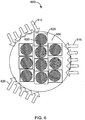
- the directional backlight may be a polygon, a circle, an ellipse, or another shape able to receive light from three different directions. Referring now to FIG. 6 , a directional backlight having a circular shape is described.
- Directional backplane 605 in directional backlight 600 receives input planar lightbeams 610-620 from three different directions.
- Each directional pixel has a circular shape, e.g., directional pixel 620, and scatters a directional lightbeam that is modulated by a modulator, e.g., LCD cell 625.
- a modulator e.g., LCD cell 625.
- Each LCD cell has a rectangular shape and the circular directional backplane 605 is designed to accommodate the rectangular LCD cells for the circular directional pixels (or for polygonal directional pixels if desired).
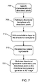
- FIG. 7 A flowchart for generating a 3D image with a directional backlight in accordance with the present application is illustrated in FIG. 7 .
- the characteristics may include characteristics of the patterned gratings in the directional pixels, such as, for example, a grating length, a grating width, an orientation, a pitch, and a duty cycle.
- each directional pixel in the directional backlight can be specified with a given set of characteristics to generate a directional lightbeam having a direction and an angular spread that is precisely controlled according to the characteristics.
- a directional backplane with directional pixels is fabricated (705).
- the directional backplane is made of a transparent material and may be fabricated with any suitable fabrication technique, such as, for example, optical lithography, nano-imprint lithography, roll-to-roll imprint lithography, direct embossing with an imprint mold, among others.
- the directional pixels may be etched in the directional backplane or be made of patterned gratings with material deposited on top of the directional backplane (e.g., any material that can be deposited and etched or lift-off, including any dielectrics or metal).
- a modulation layer (e.g., an LCD-based modulation layer) is then added to the directional backplane (710).
- the modulation layer includes a plurality of modulators (e.g., LCD cells) that are placed on top of a spacer layer (as shown in FIG. 1 ) above the directional backplane.
- the modulation layer may be designed to have a single modulator for a single directional pixel or a single modulator for a set of directional pixels.
- the directional backplane (and the directional pixels) may have different shapes (e.g., polygon, triangular, hexagonal, circular, etc.) to accommodate the modulation layer made of rectangular shaped modulators.
- the precise control that is achieved with the directional pixels and modulation in the directional backlight enables a 3D image to be generated with an easy to fabricate substantially planar structure.
- Different configurations of directional pixels generate different 3D images.
- the directional lightbeams generated by the directional pixels can be modulated to produce any desired effect in the generated images.
- the directional backlights described herein can be used to provide 3D images in display screens (e.g., in TVs, mobile devices, tablets, video game devices, and so on) as well as in other applications, such as, for example, 3D watches, 3D art devices, 3D medical devices, among others.
Landscapes
- Physics & Mathematics (AREA)
- General Physics & Mathematics (AREA)
- Optics & Photonics (AREA)
- Engineering & Computer Science (AREA)
- Multimedia (AREA)
- Signal Processing (AREA)
- Liquid Crystal (AREA)
- Testing, Inspecting, Measuring Of Stereoscopic Televisions And Televisions (AREA)
- Devices For Indicating Variable Information By Combining Individual Elements (AREA)
Description
- This application is related to
PCT Patent Application Serial No. PCT/US2012/035573 (Attorney Docket No. 82963238, Publication No.WO2013/162609 ), entitled "Directional Pixel for Use in a Display Screen", and filed on April 27th, 2012, and toPCT Patent Application Serial No. PCT/US2012/040305 (Attorney Docket No. 83011348, Publication No.WO2013/180725 ), entitled "Directional Backlight", and filed on May 31st, 2012, both assigned to the assignee of the present application. -
US2010/207964A1 describes a display device with an integrated backlight layer structure utilizing separate color diffractive out-couplings. - The ability to reproduce a light field in a display screen has been a key quest in imaging and display technology. A light field is the set of all light rays traveling in every direction through every point in space. Any natural, real-world scene can be fully characterized by its light field, providing information on the intensity, color, and direction of all light rays passing through the scene. The goal is to enable viewers of a display screen to experience a scene as one would experience it in person.
- Currently available display screens in televisions, personal computers, laptops, and mobile devices remain largely two-dimensional and are thus not capable of accurately reproducing a light field. Three-dimensional ("3D") displays have recently emerged but suffer from inefficiencies in angular and spatial resolution in addition to providing a limited number of views. Examples include 3D displays based on holograms, parallax barriers, or lenticular lenses.
- A common theme among these displays is their difficulty to generate light fields that are controlled with precision at the pixel level to achieve good image quality for a wide range of viewing angles and spatial resolutions.
- The present application discloses a directional backlight according to claim 1 and a method for generating a 3D image according to claim 8. The present application may be more fully appreciated in connection with the following detailed description taken in conjunction with the accompanying drawings, in which like reference characters refer to like parts throughout, and in which:
-
FIG. 1 illustrates a schematic diagram of a directional backlight in accordance with various examples; -
FIGS. 2A-B illustrate example top views of a directional backlight according toFIG. 1 ; -
FIGS. 3A-B illustrate further top views of a directional backlight according toFIG. 1 ; -
FIG. 4 illustrates a directional backlight having a triangular shape; -
FIG. 5 illustrates a directional backlight having an hexagonal shape; -
FIG. 6 illustrates a directional backlight having a circular shape; and -
FIG. 7 is a flowchart for generating a 3D image with a directional backlight in accordance with various examples. - A directional backlight with a modulation layer is disclosed. As generally used herein, a directional backlight is a layer in a display screen (e.g., an LCD display screen) that is used to provide a light field in the form of directional lightbeams. The directional lightbeams are scattered by a plurality of directional pixels in the directional backlight. Each directional lightbeam originates from a different directional pixel and has a given direction and angular spread based on characteristics of the directional pixel. This pointed directionality enables directional beams to be modulated (i.e., turned on, off or changed in brightness) using a plurality of modulators. The modulators may be, for example, Liquid Crystal Display ("LCD") cells (with or without polarizers). Other types of modulators may be used, such as those based on a different mechanism including micro-electrical-mechanical ("MEMS"), fluidic, magnetic, electrophoretic, or other mechanism that modulates the intensity of light upon application of an electrical signal.
- In various examples, the directional pixels are arranged in a directional backplane that is illuminated by a plurality of input planar lightbeams. The directional pixels receive the input planar lightbeams and scatter a fraction of them into directional lightbeams. A modulation layer is placed above the directional pixels to modulate the directional lightbeams as desired. The modulation layer includes a plurality of modulators (e.g., LCD cells), with each modulator modulating a single directional lightbeam from a single directional pixel or a set of directional lightbeams from a set of directional pixels. The modulation layer enables 3D images to be generated with many different views, with each view provided by a set of directional lightbeams.
- In various examples, the directional pixels in the directional backplane have patterned gratings of substantially parallel grooves arranged in or on top of the directional backplane. The directional backplane may be, for example, a slab of transparent material that guides the input planar lightbeams into the directional pixels, such as, for example, Silicon Nitride ("SiN"), glass or quartz, plastic, Indium Tin Oxide ("ITO"), among others. The patterned gratings can consist of grooves etched directly in or made of material deposited on top of the directional backplane or the waveguides (e.g., any material that can be deposited and etched or lift-off, including any dielectrics or metal). The grooves may also be slanted.
- As described in more detail herein below, each directional pixel may be specified by a grating length (i.e., dimension along the propagation axis of the input planar lightbeams), a grating width (i.e., dimension across the propagation axis of the input planar lightbeams), a groove orientation, a pitch, and a duty cycle. Each directional pixel may emit a directional lightbeam with a direction that is determined by the groove orientation and the grating pitch and with an angular spread that is determined by the grating length and width. By using a duty cycle of or around 50%, the second Fourier coefficient of the patterned gratings vanishes thereby preventing the scattering of light in additional unwanted directions. This insures that only one directional lightbeam emerges from each directional pixel regardless of its output angle.
- As further described in more detail herein below, a directional backlight can be designed with directional pixels that have a certain grating length, a grating width, a groove orientation, a pitch and a duty cycle that are selected to produce a given 3D image. The 3D image is generated from the directional lightbeams emitted by the directional pixels and modulated by the modulation layer, with modulated directional lightbeams from a set of directional pixels generating a given image view.
- It is appreciated that, in the following description, numerous specific details are set forth to provide a thorough understanding of the embodiments. However, it is appreciated that the embodiments may be practiced without limitation to these specific details. In other instances, well known methods and structures may not be described in detail to avoid unnecessarily obscuring the description of the embodiments. Also, the embodiments may be used in combination with each other.
- Referring now to
FIG. 1 , a schematic diagram of a directional backlight in accordance with various examples is described.Directional backlight 100 includes adirectional backplane 105 that receives a set of inputplanar lightbeams 110 from a plurality of light sources. The plurality of light sources may include, for example, one or more narrow-bandwidth light sources with a spectral bandwidth of approximately 30 nm or less, such as Light Emitting Diodes ("LEDs"), lasers, and so on. The inputplanar lightbeams 110 propagate in substantially the same plane as thedirectional backplane 105, which is designed to be substantially planar. - The
directional backplane 105 may consist of a slab of a transparent material (e.g., SiN, glass or quartz, plastic, ITO, etc.) having a plurality ofdirectional pixels 115a-d arranged in or on top of thedirectional backplane 105. Thedirectional pixels 115a-d scatter a fraction of the inputplanar lightbeams 110 intodirectional lightbeams 120a-d. In various examples, eachdirectional pixel 115a-d has patterned gratings of substantially parallel grooves, e.g.,grooves 125a fordirectional pixel 115a. The thickness of the grating grooves can be substantially the same for all grooves resulting in a substantially planar design. The grooves can be etched in the directional backplane or be made of material deposited on top of the directional backplane 105 (e.g., any material that can be deposited and etched or lift-off, including any dielectrics or metal). - Each
directional lightbeam 120a-d has a given direction and an angular spread that is determined by the patterned grating forming the correspondingdirectional pixel 115a-d. In particular, the direction of each directional lightbeam 120a-d is determined by the orientation and the grating pitch of the patterned gratings. The angular spread of each directional lightbeam is in turn determined by the grating length and width of the patterned gratings. For example, the direction of directional lightbeam 115a is determined by the orientation and the grating pitch of patternedgratings 125a. - It is appreciated that this substantially planar design and the formation of directional lightbeams 120a-d from input
planar lightbeams 110 requires gratings having a substantially smaller pitch than traditional diffraction gratings. For example, traditional diffraction gratings scatter light upon illumination with lightbeams that are propagating substantially across the plane of the grating. Here, the gratings in eachdirectional pixel 115a-d are substantially on the same plane as the inputplanar lightbeams 110 when generating the directional lightbeams 120a-d. - The directional lightbeams 120a-d are precisely controlled by characteristics of the gratings in
directional pixels 115a-d including a grating length L, a grating width W, a groove orientation θ, and a grating pitch Λ. In particular, the grating length L of grating 125a controls the angular spread ΔΘ of the directional lightbeam 120a along the input light propagation axis and the grating width W controls the angular spread ΔΘ of the directional lightbeam 120a across the input light propagation axis, as follows:
- The grating length L and the grating width W can vary in size in the range of 0.1 to 200 µm. The groove orientation angle θ and the grating pitch Λ may be set to satisfy a desired direction of the directional lightbeam 120a, with, for example, the groove orientation angle θ on the order of -40 to +40 degrees and the grating pitch Λ on the order of 200-700 nm.
- In various examples, a
modulation layer 130 having a plurality of modulators (e.g., LCD cells) is positioned above thedirectional pixels 115a-d to modulate the directional lightbeams 120a-d scattered by thedirectional pixels 115a-d. Modulation of directional lightbeams 120a-d involves controlling their brightness with the modulators (e.g., turning them on, off, or changing their brightness). For example, the modulators in themodulation layer 130 may be used to turn on directional lightbeams 120a and 120d and turn offdirectional lightbeams - The
modulation layer 130 may be placed on top of aspacer layer 135, which may be made of a material or simply consist of a spacing (i.e., air) between thedirectional pixels 115a-d and the modulators themodulation layer 130. Thespacer layer 135 may have a width, for example, on the order of 0-100 µm. - It is appreciated that
directional backplane 105 is shown with fourdirectional pixels 115a-d for illustration purposes only. A directional backplane in accordance with various examples can be designed with many directional pixels (e.g., higher than 100), depending on how the directional backplane is used (e.g., in a 3D display screen, in a 3D watch, in a mobile device, etc.). It is also appreciated that the directional pixels may have any shape, including for example, a circle, an ellipse, a polygon, or other geometrical shape. - Attention is now directed to
FIGS. 2A-B , which illustrate top views of a directional backlight according toFIG. 1 . InFIG. 2A ,directional backlight 200 is show with adirectional backplane 205 consisting of a plurality of polygonal directional pixels (e.g., directional pixel 210) arranged in a transparent slab. Each directional pixel is able to scatter a portion of the inputplanar lightbeams 215 into an output directional lightbeam (e.g., directional lightbeam 220). Each directional lightbeam is modulated by a modulator, e.g., LCD cell 225 fordirectional lightbeam 220. The directional lightbeams scattered by all the directional pixels in thedirectional backplane 205 and modulated by the modulators (e.g., LCD cell 225) can represent multiple image views that when combined form a 3D image. - Similarly, in
FIG. 2B ,directional backlight 230 is show with adirectional backplane 235 consisting of a plurality of circular directional pixels (e.g., directional pixel 240) arranged in a transparent slab. Each directional pixel is able to scatter a portion of the inputplanar lightbeams 245 into an output directional lightbeam (e.g., directional lightbeam 250). Each directional lightbeam is modulated by a modulator, e.g., LCD cell 255 fordirectional lightbeam 250. The directional lightbeams scattered by all the directional pixels in thedirectional backplane 235 and modulated by the modulators (e.g., LCD cell 255) can represent multiple image views that when combined form a 3D image. - In various examples, a single modulator may be used to modulate a set of directional lightbeams from a set of directional pixels. That is, a given modulator may be placed above a set of directional pixels instead of having a single modulator per directional pixel as shown in
FIGS. 2A-B . - Referring now to
FIGS. 3A-B , top views of a directional backlight according toFIG. 1 are described. InFIG. 3A ,directional backlight 300 is show with adirectional backplane 305 consisting of a plurality of polygonal directional pixels (e.g.,directional pixel 310a) arranged in a transparent slab. Each directional pixel is able to scatter a portion of the inputplanar lightbeams 315 into an output directional lightbeam (e.g., directional lightbeam 320a). A set of directional lightbeams (e.g., directional lightbeams 320a-d scattered bydirectional pixels 310a-d) is modulated by a modulator (e.g.,LCD cell 325a to modulate directional lightbeams 320a-d). For example,LCD cell 325a is used to turn ondirectional pixels 310a-d whileLCD cell 325d is used to turn offdirectional pixels 330a-d. The directional lightbeams scattered by all the directional pixels in thedirectional backplane 305 and modulated by theLCD cells 325a-d can represent multiple image views that when combined form a 3D image. - Similarly, in
FIG. 3B ,directional backlight 340 is show with adirectional backplane 345 consisting of a plurality of circular directional pixels (e.g.,directional pixel 350a) arranged in a transparent slab. Each directional pixel is able to scatter a portion of the inputplanar lightbeams 355 into an output directional lightbeam (e.g., directional lightbeam 360a). A set of directional lightbeams (e.g., directional lightbeams 360a-d scattered bydirectional pixels 350a-d) is modulated by a modulator (e.g.,LCD cell 370a to modulate directional lightbeams 360a-d). For example,LCD cell 370a is used to turn ondirectional pixels 350a-d whileLCD cell 370d is used to turn offdirectional pixels 365a-d. The directional lightbeams scattered by all the directional pixels in thedirectional backplane 345 and modulated by modulators such as theLCD cells 370a-d can represent multiple image views that when combined form a 3D image. - It is appreciated that a directional backplane may be designed to have different shapes, such as, for example, a triangular shape (as shown in
FIG. 4 ), a hexagonal shape (as shown inFIG. 5 ), or a circular shape (as shown inFIG. 6 ). InFIG. 4 , thedirectional backplane 405 receives input planar lightbeams from three different spatial directions, e.g., input planar lightbeams 410-420. This configuration may be used when the input planar lightbeams represent light of different colors, e.g., with inputplanar lightbeams 410 representing a red color, inputplanar lightbeams 415 representing a green color, and inputplanar lightbeams 420 representing a blue color. Each of the input planar lightbeams 410-420 is disposed on a side of the triangulardirectional backplane 405 to focus their light on a set of directional pixels. For example, the inputplanar lightbeams 410 is scattered into directional lightbeams by a set of directional pixels 425-435. This subset of directional pixels 425-435 may also receive light from the input planar lightbeams 415-420. However, by design this light is not scattered in the intended view zone of thedirectional backlight 400. - For example, suppose that input
planar lightbeams 410 are scattered by a subset GA of directional pixels 425-435 into an intended view zone. The intended view zone may be specified by a maximum ray angle θmax measured from a normal to thedirectional backlight 400. Inputplanar lightbeams 410 may also be scattered by a subset of directional pixels GB 440-450, however those unwanted rays are outside the intended view zone as long as:
planar lightbeams 410, neff A is the effective index of horizontal propagation of inputplanar lightbeams 410 in thedirectional backplane 405, λB is the wavelength of input planar lightbeams 420 (to be scattered by directional pixels 440-450), and neff B is the effective index of horizontal propagation of inputplanar lightbeams 420 in thedirectional backplane 405. In case where the effective indices and wavelengths are substantially the same, Equation 2 reduces to:
- It is appreciated that each directional lightbeam may be modulated by a modulator, such as, for example,
LCD cell 455. Since precise directional and angular control of directional lightbeams can be achieved with each directional pixel in thedirectional backplane 405 and the directional lightbeams can be modulated by modulators such as LCD cells, thedirectional backlight 405 can be designed to generate many different views of 3D images. - It is further appreciated that the
directional backplane 405 shown inFIG. 4 may be shaped into a more compact design by realizing that the extremities of the triangular slab can be cut to form a hexagonal shape, as shown inFIG. 5 . Thedirectional backplane 505 receives input planar lightbeams from three different spatial directions, e.g., input planar lightbeams 510-520. Each of the input planar lightbeams 510-520 is disposed on alternating sides of the hexagonaldirectional backplane 505 to focus its light on a subset of directional pixels (e.g., directional pixels 525-535). In various examples, the hexagonaldirectional backplane 505 has a side length that may range in the order of 10-30 mm, with a directional pixel size in the order of 10-30 µm. - It is appreciated that
directional backlight 500 is shown with multiple configurations of modulators. For example, a single modulator may be used to modulate directional lightbeams from a set of directional pixels, e.g.,LCD cell 540 for directional pixels 525-535, or a single modulator may be used to modulate a single directional pixel, e.g.,LCD cell 555 fordirectional pixel 560. One skilled in the art appreciates that any configuration of modulators for use with directional pixels may be used to modulate directional lightbeams scattered by the directional pixels. - It is also appreciated that the directional backlight for use with color input planar lightbeams can have any geometrical shape besides a triangular (
FIG. 4 ) or hexagonal shape (FIG. 5 ) as long as light from three primary colors is brought from three different directions. For example, the directional backlight may be a polygon, a circle, an ellipse, or another shape able to receive light from three different directions. Referring now toFIG. 6 , a directional backlight having a circular shape is described.Directional backplane 605 indirectional backlight 600 receives input planar lightbeams 610-620 from three different directions. Each directional pixel has a circular shape, e.g.,directional pixel 620, and scatters a directional lightbeam that is modulated by a modulator, e.g.,LCD cell 625. Each LCD cell has a rectangular shape and the circulardirectional backplane 605 is designed to accommodate the rectangular LCD cells for the circular directional pixels (or for polygonal directional pixels if desired). - A flowchart for generating a 3D image with a directional backlight in accordance with the present application is illustrated in
FIG. 7 . First, the characteristics of the directional pixels of the directional backlight are specified (700). The characteristics may include characteristics of the patterned gratings in the directional pixels, such as, for example, a grating length, a grating width, an orientation, a pitch, and a duty cycle. As described above, each directional pixel in the directional backlight can be specified with a given set of characteristics to generate a directional lightbeam having a direction and an angular spread that is precisely controlled according to the characteristics. - Next, a directional backplane with directional pixels is fabricated (705). The directional backplane is made of a transparent material and may be fabricated with any suitable fabrication technique, such as, for example, optical lithography, nano-imprint lithography, roll-to-roll imprint lithography, direct embossing with an imprint mold, among others. The directional pixels may be etched in the directional backplane or be made of patterned gratings with material deposited on top of the directional backplane (e.g., any material that can be deposited and etched or lift-off, including any dielectrics or metal).
- A modulation layer (e.g., an LCD-based modulation layer) is then added to the directional backplane (710). The modulation layer includes a plurality of modulators (e.g., LCD cells) that are placed on top of a spacer layer (as shown in
FIG. 1 ) above the directional backplane. As described above, the modulation layer may be designed to have a single modulator for a single directional pixel or a single modulator for a set of directional pixels. As further described above, the directional backplane (and the directional pixels) may have different shapes (e.g., polygon, triangular, hexagonal, circular, etc.) to accommodate the modulation layer made of rectangular shaped modulators. - Light from a plurality of narrow-bandwidth light sources is input into the directional backplane in the form of input planar lightbeams (715). Lastly, a 3D image is generated from the modulated directional lightbeams that are scattered by the directional pixels in the directional backplane (720).
- Advantageously, the precise control that is achieved with the directional pixels and modulation in the directional backlight enables a 3D image to be generated with an easy to fabricate substantially planar structure. Different configurations of directional pixels generate different 3D images. In addition, the directional lightbeams generated by the directional pixels can be modulated to produce any desired effect in the generated images. The directional backlights described herein can be used to provide 3D images in display screens (e.g., in TVs, mobile devices, tablets, video game devices, and so on) as well as in other applications, such as, for example, 3D watches, 3D art devices, 3D medical devices, among others.
- It is appreciated that the previous description of the disclosed embodiments is provided to enable any person skilled in the art to make or use the present disclosure. Various modifications to these embodiments will be readily apparent to those skilled in the art, and the generic principles defined herein may be applied to other embodiments without departing from the scope of the claims.
Claims (15)
- A directional backlight (100, 200, 230, 300, 340, 400, 500, 600), comprising:a directional backplane (125a, 205, 235,305, 345, 405, 505, 605) having a plurality of directional pixels (115a-d, 210, 240, 350a-d, 425-435, 525-535, 620) to scatter a plurality of input planar lightbeams (110, 215,245, 315, 355, 410-420, 510-520, 610-620) into a plurality of directional lightbeams (120a-d, 220, 250, 320a-d, 360a-d), each directional lightbeam having a direction and an angular spread controlled by characteristics of a directional pixel of the plurality of directional pixels; anda modulation layer (130) having a plurality of modulators (225, 255, 325a-d, 370a-d, 455, 555, 625) to modulate the plurality of directional lightbeams,wherein the plurality of directional pixels and plurality of modulators are configured such that the directional lightbeams scattered by the directional pixels and modulated by the modulators represent multiple image views that when combined form a 3D image.
- The directional backlight of claim 1, further comprising a spacer layer (135) between the directional backplane and the modulation layer.
- The directional backlight of claim 1, wherein the directional backplane is substantially planar.
- The directional backlight of claim 1, wherein each directional pixel in the plurality of directional pixels comprises patterned gratings with a plurality of substantially parallel grooves.
- The directional backlight of claim 1, wherein the directional backplane comprises one of a polygonal slab of transparent material and circular slab of transparent material.
- The directional backlight of claim 1, wherein the plurality of directional pixels comprises a plurality of polygonal directional pixels.
- The directional backlight of claim 1, wherein the plurality of directional pixels comprises a plurality of circular directional pixels.
- A method for generating a 3D image with a directional backlight having a modulation layer, comprising:illuminating the directional backplane with a plurality of input planar lightbeams (715), the input planar lightbeams scattered by a plurality of directional pixels into a plurality of directional lightbeams, a directional pixel of the plurality of directional pixels comprising a patterned grating having substantially parallel grooves; andmodulating the plurality of directional lightbeams with a plurality of modulators of the modulation layer to generate multiple views of a 3D image (720),wherein each directional lightbeam is controlled by characteristics of a directional pixel.
- The directional backlight of claim 5 or the method of claim 8, wherein the characteristics of a directional pixel comprise a grating length, a grating width, a grating orientation, a grating pitch, and a duty cycle.
- The directional backlight or the method of claim 9, wherein the grating pitch and the grating orientation control the direction of a directional lightbeam scattered by the directional pixel.
- The directional backlight or method of claim 9, wherein the grating length and the grating width control the angular spread of a directional lightbeam scattered by the directional pixel.
- The directional backlight of claim 1 or the method of claim 8, wherein a single modulator from the plurality of modulators modulates a directional lightbeam from a single directional pixel.
- The directional backlight of claim 1 or the method of claim 8, wherein a single modulator from the plurality of modulators modulates directional lightbeams from a set of directional pixels.
- The directional backlight of claim 1 or the method of claim 8, wherein the modulation layer comprises an LCD-based modulation layer and the plurality of modulators comprises a plurality of LCD cells.
- The method of claim 8, further comprising:fabricating the directional backplane with the plurality of directional pixels arranged thereon;adding the modulation layer above the directional backplane.
Priority Applications (3)
| Application Number | Priority Date | Filing Date | Title |
|---|---|---|---|
| EP17202907.6A EP3301504A1 (en) | 2012-06-01 | 2012-06-01 | Directional backlight with a modulation layer |
| PL12877856T PL2859402T3 (en) | 2012-06-01 | 2012-06-01 | Directional backlight with a modulation layer |
| PT128778560T PT2859402T (en) | 2012-06-01 | 2012-06-01 | Directional backlight with a modulation layer |
Applications Claiming Priority (1)
| Application Number | Priority Date | Filing Date | Title |
|---|---|---|---|
| PCT/US2012/040607 WO2013180737A1 (en) | 2012-06-01 | 2012-06-01 | Directional backlight with a modulation layer |
Related Child Applications (1)
| Application Number | Title | Priority Date | Filing Date |
|---|---|---|---|
| EP17202907.6A Division EP3301504A1 (en) | 2012-06-01 | 2012-06-01 | Directional backlight with a modulation layer |
Publications (3)
| Publication Number | Publication Date |
|---|---|
| EP2859402A1 EP2859402A1 (en) | 2015-04-15 |
| EP2859402A4 EP2859402A4 (en) | 2016-04-13 |
| EP2859402B1 true EP2859402B1 (en) | 2017-11-22 |
Family
ID=49673782
Family Applications (2)
| Application Number | Title | Priority Date | Filing Date |
|---|---|---|---|
| EP12877856.0A Active EP2859402B1 (en) | 2012-06-01 | 2012-06-01 | Directional backlight with a modulation layer |
| EP17202907.6A Withdrawn EP3301504A1 (en) | 2012-06-01 | 2012-06-01 | Directional backlight with a modulation layer |
Family Applications After (1)
| Application Number | Title | Priority Date | Filing Date |
|---|---|---|---|
| EP17202907.6A Withdrawn EP3301504A1 (en) | 2012-06-01 | 2012-06-01 | Directional backlight with a modulation layer |
Country Status (9)
| Country | Link |
|---|---|
| EP (2) | EP2859402B1 (en) |
| JP (1) | JP5964500B2 (en) |
| KR (1) | KR101788777B1 (en) |
| CN (1) | CN104335100B (en) |
| ES (1) | ES2658587T3 (en) |
| HK (1) | HK1205793A1 (en) |
| PL (1) | PL2859402T3 (en) |
| PT (1) | PT2859402T (en) |
| WO (1) | WO2013180737A1 (en) |
Families Citing this family (82)
| Publication number | Priority date | Publication date | Assignee | Title |
|---|---|---|---|---|
| GB0522968D0 (en) | 2005-11-11 | 2005-12-21 | Popovich Milan M | Holographic illumination device |
| GB0718706D0 (en) | 2007-09-25 | 2007-11-07 | Creative Physics Ltd | Method and apparatus for reducing laser speckle |
| US11726332B2 (en) | 2009-04-27 | 2023-08-15 | Digilens Inc. | Diffractive projection apparatus |
| US9335604B2 (en) | 2013-12-11 | 2016-05-10 | Milan Momcilo Popovich | Holographic waveguide display |
| US9341846B2 (en) | 2012-04-25 | 2016-05-17 | Rockwell Collins Inc. | Holographic wide angle display |
| US11204540B2 (en) | 2009-10-09 | 2021-12-21 | Digilens Inc. | Diffractive waveguide providing a retinal image |
| US9274349B2 (en) | 2011-04-07 | 2016-03-01 | Digilens Inc. | Laser despeckler based on angular diversity |
| WO2013027004A1 (en) | 2011-08-24 | 2013-02-28 | Milan Momcilo Popovich | Wearable data display |
| US10670876B2 (en) | 2011-08-24 | 2020-06-02 | Digilens Inc. | Waveguide laser illuminator incorporating a despeckler |
| WO2016020630A2 (en) | 2014-08-08 | 2016-02-11 | Milan Momcilo Popovich | Waveguide laser illuminator incorporating a despeckler |
| US20150010265A1 (en) | 2012-01-06 | 2015-01-08 | Milan, Momcilo POPOVICH | Contact image sensor using switchable bragg gratings |
| US9389415B2 (en) | 2012-04-27 | 2016-07-12 | Leia Inc. | Directional pixel for use in a display screen |
| US9456744B2 (en) | 2012-05-11 | 2016-10-04 | Digilens, Inc. | Apparatus for eye tracking |
| US9459461B2 (en) | 2012-05-31 | 2016-10-04 | Leia Inc. | Directional backlight |
| US9933684B2 (en) | 2012-11-16 | 2018-04-03 | Rockwell Collins, Inc. | Transparent waveguide display providing upper and lower fields of view having a specific light output aperture configuration |
| WO2014120160A1 (en) * | 2013-01-30 | 2014-08-07 | Hewlett-Packard Development Company, L.P. | Directional grating-based backlighting |
| US9298168B2 (en) | 2013-01-31 | 2016-03-29 | Leia Inc. | Multiview 3D wrist watch |
| US10209517B2 (en) | 2013-05-20 | 2019-02-19 | Digilens, Inc. | Holographic waveguide eye tracker |
| PL2938919T3 (en) | 2013-07-30 | 2019-06-28 | Leia Inc. | Multibeam diffraction grating-based backlighting |
| WO2015015138A1 (en) | 2013-07-31 | 2015-02-05 | Milan Momcilo Popovich | Method and apparatus for contact image sensing |
| CN104159100A (en) * | 2014-07-23 | 2014-11-19 | 京东方科技集团股份有限公司 | Stereoscopic display device and stereoscopic display method |
| US9557466B2 (en) | 2014-07-30 | 2017-01-31 | Leia, Inc | Multibeam diffraction grating-based color backlighting |
| WO2016020632A1 (en) | 2014-08-08 | 2016-02-11 | Milan Momcilo Popovich | Method for holographic mastering and replication |
| WO2016042283A1 (en) | 2014-09-19 | 2016-03-24 | Milan Momcilo Popovich | Method and apparatus for generating input images for holographic waveguide displays |
| WO2016046514A1 (en) | 2014-09-26 | 2016-03-31 | LOKOVIC, Kimberly, Sun | Holographic waveguide opticaltracker |
| JP6511144B2 (en) * | 2015-01-10 | 2019-05-15 | レイア、インコーポレイテッドLeia Inc. | Multi-beam grating based backlighting using polarization-mixing light guides and the same light guides |
| US10437064B2 (en) | 2015-01-12 | 2019-10-08 | Digilens Inc. | Environmentally isolated waveguide display |
| EP3245551B1 (en) | 2015-01-12 | 2019-09-18 | DigiLens Inc. | Waveguide light field displays |
| US10330777B2 (en) | 2015-01-20 | 2019-06-25 | Digilens Inc. | Holographic waveguide lidar |
| WO2016122679A1 (en) * | 2015-01-28 | 2016-08-04 | Leia Inc. | Three-dimensional (3d) electronic display |
| US9632226B2 (en) | 2015-02-12 | 2017-04-25 | Digilens Inc. | Waveguide grating device |
| WO2016148689A1 (en) * | 2015-03-16 | 2016-09-22 | Leia Inc. | Unidirectional grating-based backlighting employing an angularly selective reflective layer |
| US10459145B2 (en) | 2015-03-16 | 2019-10-29 | Digilens Inc. | Waveguide device incorporating a light pipe |
| US10591756B2 (en) | 2015-03-31 | 2020-03-17 | Digilens Inc. | Method and apparatus for contact image sensing |
| CN108139589B (en) * | 2015-09-05 | 2021-01-26 | 镭亚股份有限公司 | Light concentrating backlight and near-to-eye display system using the same |
| US10798371B2 (en) * | 2015-09-05 | 2020-10-06 | Leia Inc. | Multiview display with head tracking |
| CN113759555B (en) | 2015-10-05 | 2024-09-20 | 迪吉伦斯公司 | Waveguide display |
| KR102491853B1 (en) * | 2015-12-09 | 2023-01-26 | 삼성전자주식회사 | Directional backlight unit and 3D image display apparatus having the same |
| CH711992A1 (en) * | 2015-12-28 | 2017-06-30 | Regent Beleuchtungskörper Ag | Luminaire and floor lamp arrangement. |
| CN106959510A (en) * | 2016-01-08 | 2017-07-18 | 京东方科技集团股份有限公司 | A kind of display device and virtual reality glasses |
| KR102560708B1 (en) * | 2016-01-15 | 2023-07-27 | 삼성전자주식회사 | Display employing directional backlight and method for assembling the same |
| WO2017123259A1 (en) * | 2016-01-16 | 2017-07-20 | Leia Inc. | Multibeam diffraction grating-based head-up display |
| KR102526751B1 (en) * | 2016-01-25 | 2023-04-27 | 삼성전자주식회사 | Directional backlight unit, three dimensional image display apparatus, and method of displaying three dimensional image display |
| JP6776359B2 (en) * | 2016-01-30 | 2020-10-28 | レイア、インコーポレイテッドLeia Inc. | Multi-beam element backlighting with convergent view |
| JP2019510998A (en) * | 2016-01-30 | 2019-04-18 | レイア、インコーポレイテッドLeia Inc. | Privacy display and dual mode privacy display system |
| WO2017134412A1 (en) | 2016-02-04 | 2017-08-10 | Milan Momcilo Popovich | Holographic waveguide optical tracker |
| JP6895451B2 (en) | 2016-03-24 | 2021-06-30 | ディジレンズ インコーポレイテッド | Methods and Devices for Providing Polarized Selective Holography Waveguide Devices |
| JP6734933B2 (en) | 2016-04-11 | 2020-08-05 | ディジレンズ インコーポレイテッド | Holographic Waveguide Device for Structured Light Projection |
| CN105700226A (en) * | 2016-04-25 | 2016-06-22 | 京东方科技集团股份有限公司 | Viewing angle control mechanism, light guide plate, backlight module, array substrate and display panel |
| JP6645371B2 (en) * | 2016-07-15 | 2020-02-14 | オムロン株式会社 | Optical device and stereoscopic display method |
| KR102553840B1 (en) * | 2016-08-31 | 2023-07-10 | 삼성전자주식회사 | Glassless three-dimensional display apparatus including single back light unit |
| CN109642716B (en) * | 2016-09-07 | 2021-07-23 | 奇跃公司 | Virtual reality, augmented reality, and mixed reality systems including thick media and related methods |
| CN106292051B (en) * | 2016-10-21 | 2017-08-01 | 京东方科技集团股份有限公司 | A kind of display device and its display methods |
| KR102654863B1 (en) | 2016-11-08 | 2024-04-05 | 삼성전자주식회사 | Directional backlight unit, image display apparatus having the same |
| CN106443867A (en) * | 2016-11-09 | 2017-02-22 | 苏州苏大维格光电科技股份有限公司 | Waveguide device and three-dimensional display device |
| US11513350B2 (en) | 2016-12-02 | 2022-11-29 | Digilens Inc. | Waveguide device with uniform output illumination |
| US10845525B2 (en) | 2016-12-31 | 2020-11-24 | Vuzix Corporation | Imaging light guide with grating-expanded light distribution |
| FR3061461B1 (en) * | 2017-01-03 | 2020-06-19 | Valeo Vision | LIGHT WARNING SYSTEM FOR A MOTOR VEHICLE AND LIGHT WARNING METHOD |
| US10545346B2 (en) | 2017-01-05 | 2020-01-28 | Digilens Inc. | Wearable heads up displays |
| JP6618641B2 (en) | 2017-01-16 | 2019-12-11 | 三菱電機株式会社 | Texture display device, texture display method, and texture display program |
| US10416468B2 (en) | 2017-03-28 | 2019-09-17 | The Charles Stark Draper Laboratory, Inc. | Light field generator devices with series output couplers |
| WO2018186892A1 (en) * | 2017-04-08 | 2018-10-11 | Leia Inc. | Multiview backlight, mode-switchable backlight, and 2d/3d mode-switchable display |
| EP3598203B1 (en) * | 2017-04-28 | 2021-09-15 | Cloudminds (Shenzhen) Robotics Systems Co., Ltd. | Directional optical waveguide, directional backlight module and display device |
| JP7089583B2 (en) * | 2017-05-14 | 2022-06-22 | レイア、インコーポレイテッド | Multi-view backlight, display, and method with active emitter |
| JP7213831B2 (en) | 2017-06-13 | 2023-01-27 | ビュージックス コーポレーション | Image light guide with overlapping grating for expanded light distribution |
| WO2018231257A1 (en) * | 2017-06-16 | 2018-12-20 | Leia Inc. | Multiview backlight, multiview display and method employing offset multibeam elements |
| US10747176B2 (en) | 2017-09-04 | 2020-08-18 | Electronics And Telecommunications Research Institute | System and method for 3D holographic display using spatial-division multiplexed diffractive optical elements for viewing zone improvement |
| US10942430B2 (en) | 2017-10-16 | 2021-03-09 | Digilens Inc. | Systems and methods for multiplying the image resolution of a pixelated display |
| CN107741666B (en) | 2017-10-27 | 2020-08-04 | 上海天马微电子有限公司 | Display device |
| US10732569B2 (en) | 2018-01-08 | 2020-08-04 | Digilens Inc. | Systems and methods for high-throughput recording of holographic gratings in waveguide cells |
| WO2019136476A1 (en) | 2018-01-08 | 2019-07-11 | Digilens, Inc. | Waveguide architectures and related methods of manufacturing |
| CN116224492A (en) | 2018-01-08 | 2023-06-06 | 迪吉伦斯公司 | System and method for manufacturing waveguide unit |
| CN112088332A (en) | 2018-03-16 | 2020-12-15 | 迪吉伦斯公司 | Holographic waveguides including birefringence control and methods for their manufacture |
| US10345506B1 (en) * | 2018-07-16 | 2019-07-09 | Shenzhen Guangjian Technology Co., Ltd. | Light projecting method and device |
| WO2020023779A1 (en) | 2018-07-25 | 2020-01-30 | Digilens Inc. | Systems and methods for fabricating a multilayer optical structure |
| CN110908134B (en) * | 2018-08-28 | 2021-01-26 | 京东方科技集团股份有限公司 | Display device and display system |
| CN113039390B (en) * | 2018-10-31 | 2023-06-23 | 镭亚股份有限公司 | Multi-view backlight with optical mask elements, display and method |
| EP3924759A4 (en) | 2019-02-15 | 2022-12-28 | Digilens Inc. | Methods and apparatuses for providing a holographic waveguide display using integrated gratings |
| WO2020186113A1 (en) | 2019-03-12 | 2020-09-17 | Digilens Inc. | Holographic waveguide backlight and related methods of manufacturing |
| KR20220016990A (en) | 2019-06-07 | 2022-02-10 | 디지렌즈 인코포레이티드. | Waveguides incorporating transmission and reflection gratings and related manufacturing methods |
| JP2022543571A (en) | 2019-07-29 | 2022-10-13 | ディジレンズ インコーポレイテッド | Method and Apparatus for Multiplying Image Resolution and Field of View for Pixelated Displays |
| JP2022546413A (en) | 2019-08-29 | 2022-11-04 | ディジレンズ インコーポレイテッド | Vacuum grating and manufacturing method |
Family Cites Families (17)
| Publication number | Priority date | Publication date | Assignee | Title |
|---|---|---|---|---|
| EP1068548B1 (en) * | 1998-04-02 | 2003-11-12 | Elop Electro-Optics Industries Ltd. | Holographic optical devices |
| FI106323B (en) * | 1998-12-30 | 2001-01-15 | Nokia Mobile Phones Ltd | Backlight light guide for flat screen |
| US6919950B2 (en) * | 2000-08-29 | 2005-07-19 | Roman S. Dabrowski | Liquid crystal device and a liquid crystal material |
| JP2004077897A (en) * | 2002-08-20 | 2004-03-11 | Nippon Telegr & Teleph Corp <Ntt> | Display |
| EP1666992A1 (en) * | 2004-12-02 | 2006-06-07 | Asulab S.A. | Timepiece comprising a luminous decoration |
| EP1666933A1 (en) * | 2004-12-02 | 2006-06-07 | Asulab S.A. | Dual illumination function optical device and figurative image formation |
| WO2007042852A1 (en) * | 2005-10-13 | 2007-04-19 | Nokia Corporation | Illumination method for displaying different graphical layouts |
| US7714368B2 (en) * | 2006-06-26 | 2010-05-11 | Aptina Imaging Corporation | Method and apparatus providing imager pixel array with grating structure and imager device containing the same |
| CN101501391B (en) | 2006-07-03 | 2011-10-12 | 诺基亚公司 | Changing graphics in an apparatus including user interface illumination |
| JP5157115B2 (en) * | 2006-09-28 | 2013-03-06 | 凸版印刷株式会社 | Display comprising diffraction grating and printed matter using the same |
| US20080204873A1 (en) * | 2007-02-23 | 2008-08-28 | Strategic Patent Acquisitions Llc | Techniques for three dimensional displays |
| US7507012B2 (en) * | 2007-05-16 | 2009-03-24 | Rohm And Haas Denmark Finance A/S | LCD displays with light redirection |
| EP2158518B1 (en) * | 2007-06-14 | 2015-01-14 | Nokia Corporation | Displays with integrated backlighting |
| TWI387316B (en) * | 2008-11-18 | 2013-02-21 | Ind Tech Res Inst | Stereoscopic image displaying apparatus and stereoscopic image displaying method |
| JP2010237416A (en) | 2009-03-31 | 2010-10-21 | Sharp Corp | Stereoscopic display device |
| JP5493978B2 (en) * | 2010-02-19 | 2014-05-14 | 凸版印刷株式会社 | Image display body and information medium |
| JP2011133677A (en) * | 2009-12-24 | 2011-07-07 | Toppan Printing Co Ltd | Blank medium, image display body, and information medium |
-
2012
- 2012-06-01 WO PCT/US2012/040607 patent/WO2013180737A1/en active Application Filing
- 2012-06-01 KR KR1020147027174A patent/KR101788777B1/en active IP Right Grant
- 2012-06-01 EP EP12877856.0A patent/EP2859402B1/en active Active
- 2012-06-01 EP EP17202907.6A patent/EP3301504A1/en not_active Withdrawn
- 2012-06-01 JP JP2015514974A patent/JP5964500B2/en active Active
- 2012-06-01 ES ES12877856.0T patent/ES2658587T3/en active Active
- 2012-06-01 PT PT128778560T patent/PT2859402T/en unknown
- 2012-06-01 CN CN201280072700.0A patent/CN104335100B/en active Active
- 2012-06-01 PL PL12877856T patent/PL2859402T3/en unknown
-
2015
- 2015-07-06 HK HK15106381.7A patent/HK1205793A1/en unknown
Non-Patent Citations (1)
| Title |
|---|
| None * |
Also Published As
| Publication number | Publication date |
|---|---|
| HK1205793A1 (en) | 2015-12-24 |
| JP2015530604A (en) | 2015-10-15 |
| EP3301504A1 (en) | 2018-04-04 |
| PL2859402T3 (en) | 2018-08-31 |
| PT2859402T (en) | 2018-02-08 |
| EP2859402A4 (en) | 2016-04-13 |
| KR20150021017A (en) | 2015-02-27 |
| WO2013180737A1 (en) | 2013-12-05 |
| CN104335100B (en) | 2017-06-13 |
| JP5964500B2 (en) | 2016-08-03 |
| ES2658587T3 (en) | 2018-03-12 |
| CN104335100A (en) | 2015-02-04 |
| KR101788777B1 (en) | 2017-10-20 |
| EP2859402A1 (en) | 2015-04-15 |
Similar Documents
| Publication | Publication Date | Title |
|---|---|---|
| EP2859402B1 (en) | Directional backlight with a modulation layer | |
| US10082613B2 (en) | Directional backlight with a modulation layer | |
| US10120198B2 (en) | Directional backlight | |
| EP2856244B1 (en) | Directional backlight | |
| US9785119B2 (en) | Multiview display screen and multiview mobile device using same | |
| EP2951649B1 (en) | Multiview 3d wrist watch | |
| CN108139589B (en) | Light concentrating backlight and near-to-eye display system using the same | |
| WO2014081415A1 (en) | Directional waveguide-based pixel for use in a multiview display screen | |
| WO2014051623A1 (en) | Directional waveguide-based backlight for use in a multivew display screen | |
| US10488702B2 (en) | Display device having diffraction grating structure and driving method for the same | |
| WO2017118007A1 (en) | Dual-view autostereoscopic display device, method of manufacturing same, and liquid crystal display device | |
| CN107278274B (en) | Directional optical waveguide, directional backlight module and display device | |
| CN112400133A (en) | 3D display | |
| CN118011647A (en) | Spatial light modulation assembly, holographic display system and electronic equipment |
Legal Events
| Date | Code | Title | Description |
|---|---|---|---|
| PUAI | Public reference made under article 153(3) epc to a published international application that has entered the european phase |
Free format text: ORIGINAL CODE: 0009012 |
|
| 17P | Request for examination filed |
Effective date: 20141215 |
|
| AK | Designated contracting states |
Kind code of ref document: A1 Designated state(s): AL AT BE BG CH CY CZ DE DK EE ES FI FR GB GR HR HU IE IS IT LI LT LU LV MC MK MT NL NO PL PT RO RS SE SI SK SM TR |
|
| AX | Request for extension of the european patent |
Extension state: BA ME |
|
| DAX | Request for extension of the european patent (deleted) | ||
| RA4 | Supplementary search report drawn up and despatched (corrected) |
Effective date: 20160310 |
|
| RIC1 | Information provided on ipc code assigned before grant |
Ipc: F21V 8/00 20060101ALI20160304BHEP Ipc: G02B 27/10 20060101ALI20160304BHEP Ipc: G02B 27/22 20060101AFI20160304BHEP Ipc: H04N 13/04 20060101ALI20160304BHEP |
|
| GRAP | Despatch of communication of intention to grant a patent |
Free format text: ORIGINAL CODE: EPIDOSNIGR1 |
|
| INTG | Intention to grant announced |
Effective date: 20170421 |
|
| GRAS | Grant fee paid |
Free format text: ORIGINAL CODE: EPIDOSNIGR3 |
|
| GRAJ | Information related to disapproval of communication of intention to grant by the applicant or resumption of examination proceedings by the epo deleted |
Free format text: ORIGINAL CODE: EPIDOSDIGR1 |
|
| GRAL | Information related to payment of fee for publishing/printing deleted |
Free format text: ORIGINAL CODE: EPIDOSDIGR3 |
|
| GRAJ | Information related to disapproval of communication of intention to grant by the applicant or resumption of examination proceedings by the epo deleted |
Free format text: ORIGINAL CODE: EPIDOSDIGR1 |
|
| GRAP | Despatch of communication of intention to grant a patent |
Free format text: ORIGINAL CODE: EPIDOSNIGR1 |
|
| GRAR | Information related to intention to grant a patent recorded |
Free format text: ORIGINAL CODE: EPIDOSNIGR71 |
|
| GRAA | (expected) grant |
Free format text: ORIGINAL CODE: 0009210 |
|
| INTC | Intention to grant announced (deleted) | ||
| AK | Designated contracting states |
Kind code of ref document: B1 Designated state(s): AL AT BE BG CH CY CZ DE DK EE ES FI FR GB GR HR HU IE IS IT LI LT LU LV MC MK MT NL NO PL PT RO RS SE SI SK SM TR |
|
| INTG | Intention to grant announced |
Effective date: 20171018 |
|
| REG | Reference to a national code |
Ref country code: GB Ref legal event code: FG4D |
|
| REG | Reference to a national code |
Ref country code: CH Ref legal event code: EP |
|
| REG | Reference to a national code |
Ref country code: IE Ref legal event code: FG4D |
|
| REG | Reference to a national code |
Ref country code: AT Ref legal event code: REF Ref document number: 948921 Country of ref document: AT Kind code of ref document: T Effective date: 20171215 |
|
| REG | Reference to a national code |
Ref country code: DE Ref legal event code: R096 Ref document number: 602012040218 Country of ref document: DE |
|
| REG | Reference to a national code |
Ref country code: PT Ref legal event code: SC4A Ref document number: 2859402 Country of ref document: PT Date of ref document: 20180208 Kind code of ref document: T Free format text: AVAILABILITY OF NATIONAL TRANSLATION Effective date: 20180201 |
|
| REG | Reference to a national code |
Ref country code: NL Ref legal event code: FP |
|
| REG | Reference to a national code |
Ref country code: ES Ref legal event code: FG2A Ref document number: 2658587 Country of ref document: ES Kind code of ref document: T3 Effective date: 20180312 |
|
| REG | Reference to a national code |
Ref country code: LT Ref legal event code: MG4D |
|
| REG | Reference to a national code |
Ref country code: FR Ref legal event code: PLFP Year of fee payment: 7 |
|
| REG | Reference to a national code |
Ref country code: CH Ref legal event code: NV Representative=s name: E. BLUM AND CO. AG PATENT- UND MARKENANWAELTE , CH |
|
| REG | Reference to a national code |
Ref country code: AT Ref legal event code: MK05 Ref document number: 948921 Country of ref document: AT Kind code of ref document: T Effective date: 20171122 |
|
| PG25 | Lapsed in a contracting state [announced via postgrant information from national office to epo] |
Ref country code: FI Free format text: LAPSE BECAUSE OF FAILURE TO SUBMIT A TRANSLATION OF THE DESCRIPTION OR TO PAY THE FEE WITHIN THE PRESCRIBED TIME-LIMIT Effective date: 20171122 Ref country code: LT Free format text: LAPSE BECAUSE OF FAILURE TO SUBMIT A TRANSLATION OF THE DESCRIPTION OR TO PAY THE FEE WITHIN THE PRESCRIBED TIME-LIMIT Effective date: 20171122 Ref country code: SE Free format text: LAPSE BECAUSE OF FAILURE TO SUBMIT A TRANSLATION OF THE DESCRIPTION OR TO PAY THE FEE WITHIN THE PRESCRIBED TIME-LIMIT Effective date: 20171122 Ref country code: NO Free format text: LAPSE BECAUSE OF FAILURE TO SUBMIT A TRANSLATION OF THE DESCRIPTION OR TO PAY THE FEE WITHIN THE PRESCRIBED TIME-LIMIT Effective date: 20180222 |
|
| PG25 | Lapsed in a contracting state [announced via postgrant information from national office to epo] |
Ref country code: RS Free format text: LAPSE BECAUSE OF FAILURE TO SUBMIT A TRANSLATION OF THE DESCRIPTION OR TO PAY THE FEE WITHIN THE PRESCRIBED TIME-LIMIT Effective date: 20171122 Ref country code: GR Free format text: LAPSE BECAUSE OF FAILURE TO SUBMIT A TRANSLATION OF THE DESCRIPTION OR TO PAY THE FEE WITHIN THE PRESCRIBED TIME-LIMIT Effective date: 20180223 Ref country code: BG Free format text: LAPSE BECAUSE OF FAILURE TO SUBMIT A TRANSLATION OF THE DESCRIPTION OR TO PAY THE FEE WITHIN THE PRESCRIBED TIME-LIMIT Effective date: 20180222 Ref country code: LV Free format text: LAPSE BECAUSE OF FAILURE TO SUBMIT A TRANSLATION OF THE DESCRIPTION OR TO PAY THE FEE WITHIN THE PRESCRIBED TIME-LIMIT Effective date: 20171122 Ref country code: HR Free format text: LAPSE BECAUSE OF FAILURE TO SUBMIT A TRANSLATION OF THE DESCRIPTION OR TO PAY THE FEE WITHIN THE PRESCRIBED TIME-LIMIT Effective date: 20171122 Ref country code: AT Free format text: LAPSE BECAUSE OF FAILURE TO SUBMIT A TRANSLATION OF THE DESCRIPTION OR TO PAY THE FEE WITHIN THE PRESCRIBED TIME-LIMIT Effective date: 20171122 |
|
| PG25 | Lapsed in a contracting state [announced via postgrant information from national office to epo] |
Ref country code: EE Free format text: LAPSE BECAUSE OF FAILURE TO SUBMIT A TRANSLATION OF THE DESCRIPTION OR TO PAY THE FEE WITHIN THE PRESCRIBED TIME-LIMIT Effective date: 20171122 Ref country code: CY Free format text: LAPSE BECAUSE OF FAILURE TO SUBMIT A TRANSLATION OF THE DESCRIPTION OR TO PAY THE FEE WITHIN THE PRESCRIBED TIME-LIMIT Effective date: 20171122 Ref country code: DK Free format text: LAPSE BECAUSE OF FAILURE TO SUBMIT A TRANSLATION OF THE DESCRIPTION OR TO PAY THE FEE WITHIN THE PRESCRIBED TIME-LIMIT Effective date: 20171122 Ref country code: SK Free format text: LAPSE BECAUSE OF FAILURE TO SUBMIT A TRANSLATION OF THE DESCRIPTION OR TO PAY THE FEE WITHIN THE PRESCRIBED TIME-LIMIT Effective date: 20171122 Ref country code: CZ Free format text: LAPSE BECAUSE OF FAILURE TO SUBMIT A TRANSLATION OF THE DESCRIPTION OR TO PAY THE FEE WITHIN THE PRESCRIBED TIME-LIMIT Effective date: 20171122 |
|
| REG | Reference to a national code |
Ref country code: DE Ref legal event code: R097 Ref document number: 602012040218 Country of ref document: DE |
|
| PG25 | Lapsed in a contracting state [announced via postgrant information from national office to epo] |
Ref country code: RO Free format text: LAPSE BECAUSE OF FAILURE TO SUBMIT A TRANSLATION OF THE DESCRIPTION OR TO PAY THE FEE WITHIN THE PRESCRIBED TIME-LIMIT Effective date: 20171122 Ref country code: SM Free format text: LAPSE BECAUSE OF FAILURE TO SUBMIT A TRANSLATION OF THE DESCRIPTION OR TO PAY THE FEE WITHIN THE PRESCRIBED TIME-LIMIT Effective date: 20171122 |
|
| PLBE | No opposition filed within time limit |
Free format text: ORIGINAL CODE: 0009261 |
|
| STAA | Information on the status of an ep patent application or granted ep patent |
Free format text: STATUS: NO OPPOSITION FILED WITHIN TIME LIMIT |
|
| 26N | No opposition filed |
Effective date: 20180823 |
|
| PG25 | Lapsed in a contracting state [announced via postgrant information from national office to epo] |
Ref country code: SI Free format text: LAPSE BECAUSE OF FAILURE TO SUBMIT A TRANSLATION OF THE DESCRIPTION OR TO PAY THE FEE WITHIN THE PRESCRIBED TIME-LIMIT Effective date: 20171122 |
|
| PG25 | Lapsed in a contracting state [announced via postgrant information from national office to epo] |
Ref country code: MC Free format text: LAPSE BECAUSE OF FAILURE TO SUBMIT A TRANSLATION OF THE DESCRIPTION OR TO PAY THE FEE WITHIN THE PRESCRIBED TIME-LIMIT Effective date: 20171122 Ref country code: LU Free format text: LAPSE BECAUSE OF NON-PAYMENT OF DUE FEES Effective date: 20180601 |
|
| REG | Reference to a national code |
Ref country code: DE Ref legal event code: R079 Ref document number: 602012040218 Country of ref document: DE Free format text: PREVIOUS MAIN CLASS: G02B0027220000 Ipc: G02B0030000000 |
|
| PG25 | Lapsed in a contracting state [announced via postgrant information from national office to epo] |
Ref country code: MT Free format text: LAPSE BECAUSE OF NON-PAYMENT OF DUE FEES Effective date: 20180601 |
|
| PG25 | Lapsed in a contracting state [announced via postgrant information from national office to epo] |
Ref country code: TR Free format text: LAPSE BECAUSE OF FAILURE TO SUBMIT A TRANSLATION OF THE DESCRIPTION OR TO PAY THE FEE WITHIN THE PRESCRIBED TIME-LIMIT Effective date: 20171122 |
|
| PG25 | Lapsed in a contracting state [announced via postgrant information from national office to epo] |
Ref country code: MK Free format text: LAPSE BECAUSE OF NON-PAYMENT OF DUE FEES Effective date: 20171122 Ref country code: HU Free format text: LAPSE BECAUSE OF FAILURE TO SUBMIT A TRANSLATION OF THE DESCRIPTION OR TO PAY THE FEE WITHIN THE PRESCRIBED TIME-LIMIT; INVALID AB INITIO Effective date: 20120601 |
|
| PG25 | Lapsed in a contracting state [announced via postgrant information from national office to epo] |
Ref country code: AL Free format text: LAPSE BECAUSE OF FAILURE TO SUBMIT A TRANSLATION OF THE DESCRIPTION OR TO PAY THE FEE WITHIN THE PRESCRIBED TIME-LIMIT Effective date: 20171122 Ref country code: IS Free format text: LAPSE BECAUSE OF FAILURE TO SUBMIT A TRANSLATION OF THE DESCRIPTION OR TO PAY THE FEE WITHIN THE PRESCRIBED TIME-LIMIT Effective date: 20180322 |
|
| REG | Reference to a national code |
Ref country code: FR Ref legal event code: PLFP Year of fee payment: 12 |
|
| PGFP | Annual fee paid to national office [announced via postgrant information from national office to epo] |
Ref country code: IT Payment date: 20230510 Year of fee payment: 12 |
|
| PGFP | Annual fee paid to national office [announced via postgrant information from national office to epo] |
Ref country code: ES Payment date: 20230707 Year of fee payment: 12 Ref country code: CH Payment date: 20230702 Year of fee payment: 12 |
|
| PGFP | Annual fee paid to national office [announced via postgrant information from national office to epo] |
Ref country code: IE Payment date: 20240619 Year of fee payment: 13 |
|
| PGFP | Annual fee paid to national office [announced via postgrant information from national office to epo] |
Ref country code: GB Payment date: 20240620 Year of fee payment: 13 |
|
| PGFP | Annual fee paid to national office [announced via postgrant information from national office to epo] |
Ref country code: DE Payment date: 20240619 Year of fee payment: 13 |
|
| PGFP | Annual fee paid to national office [announced via postgrant information from national office to epo] |
Ref country code: NL Payment date: 20240619 Year of fee payment: 13 |
|
| PGFP | Annual fee paid to national office [announced via postgrant information from national office to epo] |
Ref country code: FR Payment date: 20240628 Year of fee payment: 13 |
|
| PGFP | Annual fee paid to national office [announced via postgrant information from national office to epo] |
Ref country code: PL Payment date: 20240523 Year of fee payment: 13 Ref country code: PT Payment date: 20240523 Year of fee payment: 13 |
|
| PGFP | Annual fee paid to national office [announced via postgrant information from national office to epo] |
Ref country code: BE Payment date: 20240619 Year of fee payment: 13 |