EP2858246A1 - Capacitance minimization switch - Google Patents
Capacitance minimization switch Download PDFInfo
- Publication number
- EP2858246A1 EP2858246A1 EP13368037.1A EP13368037A EP2858246A1 EP 2858246 A1 EP2858246 A1 EP 2858246A1 EP 13368037 A EP13368037 A EP 13368037A EP 2858246 A1 EP2858246 A1 EP 2858246A1
- Authority
- EP
- European Patent Office
- Prior art keywords
- transmission gate
- current
- amplifier
- cmos transmission
- input
- Prior art date
- Legal status (The legal status is an assumption and is not a legal conclusion. Google has not performed a legal analysis and makes no representation as to the accuracy of the status listed.)
- Granted
Links
Images


Classifications
-
- H—ELECTRICITY
- H03—ELECTRONIC CIRCUITRY
- H03F—AMPLIFIERS
- H03F3/00—Amplifiers with only discharge tubes or only semiconductor devices as amplifying elements
- H03F3/45—Differential amplifiers
- H03F3/45071—Differential amplifiers with semiconductor devices only
- H03F3/45076—Differential amplifiers with semiconductor devices only characterised by the way of implementation of the active amplifying circuit in the differential amplifier
- H03F3/45179—Differential amplifiers with semiconductor devices only characterised by the way of implementation of the active amplifying circuit in the differential amplifier using MOSFET transistors as the active amplifying circuit
-
- H—ELECTRICITY
- H03—ELECTRONIC CIRCUITRY
- H03F—AMPLIFIERS
- H03F1/00—Details of amplifiers with only discharge tubes, only semiconductor devices or only unspecified devices as amplifying elements
- H03F1/08—Modifications of amplifiers to reduce detrimental influences of internal impedances of amplifying elements
- H03F1/083—Modifications of amplifiers to reduce detrimental influences of internal impedances of amplifying elements in transistor amplifiers
- H03F1/086—Modifications of amplifiers to reduce detrimental influences of internal impedances of amplifying elements in transistor amplifiers with FET's
-
- H—ELECTRICITY
- H03—ELECTRONIC CIRCUITRY
- H03K—PULSE TECHNIQUE
- H03K17/00—Electronic switching or gating, i.e. not by contact-making and –breaking
- H03K17/14—Modifications for compensating variations of physical values, e.g. of temperature
- H03K17/145—Modifications for compensating variations of physical values, e.g. of temperature in field-effect transistor switches
-
- H—ELECTRICITY
- H03—ELECTRONIC CIRCUITRY
- H03K—PULSE TECHNIQUE
- H03K17/00—Electronic switching or gating, i.e. not by contact-making and –breaking
- H03K17/16—Modifications for eliminating interference voltages or currents
- H03K17/161—Modifications for eliminating interference voltages or currents in field-effect transistor switches
-
- H—ELECTRICITY
- H03—ELECTRONIC CIRCUITRY
- H03K—PULSE TECHNIQUE
- H03K2217/00—Indexing scheme related to electronic switching or gating, i.e. not by contact-making or -breaking covered by H03K17/00
- H03K2217/0054—Gating switches, e.g. pass gates
Definitions
- the present disclosure is related to integrated circuit switches, and in particular with switches designed to minimize effects of parasitic capacitance.
- Switches are utilized in electronic circuits to control when a signal is allowed to propagate from one node to another.
- An implementation of such a switch in CMOS technology is the transmission gate (examples shown in FIG. 1A and 1B ), comprising NMOS and PMOS transistors connected in parallel for the purpose of allowing good conductivity for a wide signal voltage range.
- FIG. 1A a data switch of prior art comprising an N-channel transistor 10 and a P-channel transistor 11 connected in parallel, where the sources of the two transistors are connected together to form a data input A and the drains of the two transistors are connected to form data output B.
- An ON signal a high logic signal, is applied to the gate of the N-channel transistor 10 and through an inverter circuit 12 to the gate of the P-channel transistor 11.
- an off signal which is a low logic signal, is applied to the gate of the N-channel transistor and through the inverter circuit to the gate of the P-channel transistor.
- FIG. 1B is a second data switch of prior art where a second parallel connected pair of transistors, an N-channel transistor 15 and a P-channel transistor 16, are connected in tandem 13 with a first pair of transistors 10 and 11.
- An N-channel transistor 14 is used to ground the tandem connection 13 to insure isolation between A and B.
- a semiconductor switch presents a resistance to AC signals inside the intended operating range, but parasitic capacitance is also present.
- the impedance of the parasitic capacitive will present an AC path to the power supplies and chip substrate, and will ultimately cause signal attenuation at higher frequencies.
- there will be capacitive impedance between the two sides of the switch that will cause some signal propagation when in the "off' state, thus reducing the isolation of the switch against higher frequency signals.
- a disadvantage of prior-art switch design shown in FIG. 1A is that lower resistive impedance in the "on" state dictates larger transistors. Larger transistors inherently include larger unwanted capacitances; therefore strong switches with low on-resistance also have larger parasitic capacitances, which limit the maximum frequency of a switched signal.
- ⁇ Q the sum of all parasitic capacitances multiplied by the change in voltage
- US 2006/0164164 A1 (Rogers et al. ) is directed to compensating for parasitic capacitances in a VCA circuit.
- US 8,400,848 B2 (Fujimura ) is directed to a bit line capacitance compensation capacitor, which compensates the capacitance of the bit line, and a peripheral capacitance compensation capacitor, which compensates the peripheral capacitance of the bit line.
- a capacitance compensation is directed to using a compensation device coupled to a gain device.
- US 8,344,802 B2 (Huang et al. ) is directed to an operational amplifier device capable of using transmission gates for capacitance compensation.
- US 6,462,611 B2 (Shigehara et al. ) is directed to body effect compensation for electronic switches connected between two terminals.
- US 6,150,884 (Fattaruso ) an improved operational amplifier circuit with nested transconductance is directed to capacitance compensation.
- It is objectives of the present disclosure is to sense current diverted from a CMOS transmission gate and inject that current into the input of the transmission gate.
- the present disclosure would not work without the use of some element that senses the rate of change of voltage of the signal being propagated by the switch, ( dv / dt ) .
- dv / dt is sensed by a simple RC network and an operational transconductance amplifier (OTA).
- OTA operational transconductance amplifier
- these required sensing and scaling functions are performed in one step by measuring the current that flows through the parasitic gate capacitance towards V+ (for the NMOS in the example) or V-(for the PMOS in the example).
- the current is proportional to both the capacitance and dv / dt.
- the present disclosure also would not work without converting the measurement of the current in the parasitic capacitances into another current, which is sourced from the local power supply(ies) and is fed into the signal at node A or B, or both A and B, or at any node in-between which has equal electrical potential in the "on " state.
- the current that is fed back into the system must be of opposite polarity to the current flowing into the system through the parasitic devices. For example, raising the voltage of node A in FIG. 3a requires that current must flow from nodes A and B into the output of the inverter via the gate capacitance of the PMOS transistor, therefore the OTA must deliver some current back into node A.
- FIG. 2A shows the most significant parasitic capacitances present in the simple transmission gate of FIG. 1a and reduced to a simple model in FIG. 2B .
- FIG. 2A is shown the main parasitic capacitances 20 associated with N-channel transistor and 21 associated with the P-channel transistor of a CMOS transmission gate, which affect signals that are switched from A to B. These capacitances include input capacitance from A to the gate of each transistor and from A to the substrate of each capacitor, and output capacitance from B to the gate of each transistor and B to the substrate of each transistor.
- FIG. 2B shows an equivalent circuit of the switch of FIG.
- the two transistors of the switch are represented by a parallel resistance Rp to signals flowing from A to B, where Rp is a high value when the switch is biased off with a low logic signal, and Rp is a low resistance when the switch is biased on with a high logic signal.
- the input capacitance Cps is the equivalent of the parallel parasitic capacitance of the two transistors at point A and the output capacitance Cpd is the equivalent of the parallel parasitic capacitance of the two transistors at point B.
- FIG. 3A a CMOS transmission gate 31 of the present disclosure is shown.
- the rate of change of an input signal voltage is sensed through a dedicated RC network.
- the sense capacitor, C will add to the parasitic capacitance of the switch.
- An OTA (operational transconductance amplifier) 30 measures a current, i RC , by measuring the voltage drop, V R , across the resistor R of the RC network.
- the output of the OTC is applied back to the input of the CMOS transmission gate.
- the gain, g m of the OTA (operational transconductance amplifier) must be correctly set to account for the values of sense resistor, R, sense capacitor, C, and total parasitic capacitance, C para (which includes sense capacitance, C).
- the parasitic capacitance does not need to be known because it is sensed directly by current amplifiers 32 and 33.
- a first input to current amplifier 32 is connected to the gate of the N-channel transistor of the CMOS transmission gate 31 and a first input to current amplifier 33 is connected to the gate of the P-channel transistor.
- the second input to current amplifier 32 is connected to the CMOS transmission gate on/off input and the second input to current amplifier 33 is connected to the output of the inverter circuit 34, which is connected to the transmission gate on/off input.
- the most dominate current that is "lost" through the parasitic capacitance surrounding the transistor gates is sensed directly and mirrored back into the signal path. For this reason, the size of the transistors is unimportant and the same compensation circuit can be applied to any size of switch, providing that the maximum current, accuracy, and speed are suitable.
- the gain of the two current amplifiers 32 and 33 is set to be less than unity to insure circuit stability; therefore, the amount of compensation of the effects of the parasitic capacitance is somewhat less than one hundred percent. However, most of the loss through the parasitic capacitance is compensated.
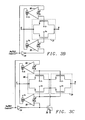
- FIG. 3C the same concept as in FIG. 3B is applied to a transistor switch architecture, which provides better isolation in the "off' state.
- CMOS transmission switches 36 and 37 connected in tandem.
- An N-channel transistor 39 is used to ground the tandem connection to insure isolation between input A and output B of the tandem switch.
- the gates of the two N-channel transistors are connected together and connected to a first input of current amplifier 32.
- the second input to the current amplifier 32 is connected to on/off control input of the tandem transistor switch.
- the output of amplifier 32 is connected to input A of the tandem transistor switch.
- the gates of the two P-channel transistors are connected together and connected to a first input to current amplifier 33.
- the second input to current amplifier 33 is connected to the output of the inverter circuit 34, and the output of current amplifier 33 is connected to input A of the tandem transistor switch.
- the gain of the current amplifiers 32 and 33 is set to be less than one (1) to maintain stability of the circuitry since the feedback that is accomplished is positive feedback.
- any type of capacitor might be suitable for emulating the parasitic capacitance before scaling (capacitor C in FIG. 3A ), however the most suitable type of capacitor would probably be a MOSCAP (capacitor formed across the gate-oxide of a MOS transistor), since the MOSCAP could be matched to the dimension, orientation, and electrical characteristics of the switch transistor. Such matching would lead to a roughly constant relationship between the sensed current and the total lost current.
- MOSCAP capacitor formed across the gate-oxide of a MOS transistor
- USB data signals transmitted on two separate wires
- USB data signals should have a differential amplitude between 200mV - 400mV, switching at speeds from 1.5Mb/s (low-speed), to 12Mb/s (full-speed), 480Mb/s (high-speed), and 5Gb/s (Super-Speed).
- Data lines are terminated by impedances from 18 ⁇ to 45 ⁇ and the data integrity relies on the ability of the data-line to pass signals from the transmitter to the receiver without large overshoots or attenuation.
- the ideal data line would have zero capacitance and zero impedance, allowing the transmitter and receiver to completely define the signal characteristics as defined in the USB standard specifications. But when multiplexing is required to facilitate the sharing of 2 pins for multiple functions, one of these being USB data communication, then inevitably a switch will be required in the data-line which will add additional capacitance and impedance. To get as close to the ideal data-line as possible, the switch should be low impedance (meaning it will be large), and should introduce minimum capacitance. Because larger switches introduce larger capacitance, the capacitance minimization concept described in this invention can be used.
Landscapes
- Engineering & Computer Science (AREA)
- Power Engineering (AREA)
- Amplifiers (AREA)
- Electronic Switches (AREA)
Abstract
Description
- The present disclosure is related to integrated circuit switches, and in particular with switches designed to minimize effects of parasitic capacitance.
- Semiconductor switches are utilized in electronic circuits to control when a signal is allowed to propagate from one node to another. An implementation of such a switch in CMOS technology is the transmission gate (examples shown in
FIG. 1A and 1B ), comprising NMOS and PMOS transistors connected in parallel for the purpose of allowing good conductivity for a wide signal voltage range. There are a number of different ways in which combinations of transistors can be connected together to implement a switch function; however, they all perform the same basic function of connecting two nodes when "on", and isolating the two nodes when "off". For DC signals inside an intended operating range, a switch appears like a resistor, the impedance depending on the architecture used and the dimensions of the transistors. There can also be dependence on the DC level of the signal for most architectures. - In
FIG. 1A is shown a data switch of prior art comprising an N-channel transistor 10 and a P-channel transistor 11 connected in parallel, where the sources of the two transistors are connected together to form a data input A and the drains of the two transistors are connected to form data output B. An ON signal, a high logic signal, is applied to the gate of the N-channel transistor 10 and through aninverter circuit 12 to the gate of the P-channel transistor 11. To turn off the switch an off signal, which is a low logic signal, is applied to the gate of the N-channel transistor and through the inverter circuit to the gate of the P-channel transistor. - In
FIG. 1B is a second data switch of prior art where a second parallel connected pair of transistors, an N-channel transistor 15 and a P-channel transistor 16, are connected intandem 13 with a first pair oftransistors channel transistor 14 is used to ground thetandem connection 13 to insure isolation between A and B. - A semiconductor switch presents a resistance to AC signals inside the intended operating range, but parasitic capacitance is also present. The impedance of the parasitic capacitive will present an AC path to the power supplies and chip substrate, and will ultimately cause signal attenuation at higher frequencies. In addition there will be capacitive impedance between the two sides of the switch that will cause some signal propagation when in the "off' state, thus reducing the isolation of the switch against higher frequency signals. A disadvantage of prior-art switch design shown in
FIG. 1A is that lower resistive impedance in the "on" state dictates larger transistors. Larger transistors inherently include larger unwanted capacitances; therefore strong switches with low on-resistance also have larger parasitic capacitances, which limit the maximum frequency of a switched signal. - The purpose of the switches in
FIG. 1A and 1B is to make the voltage at node B equal to the voltage at node A while in the "on" state. Any change in the signal voltage at nodes A and B will require the total sum of all parasitic capacitances to be charged, or discharged, by a charge, ΔQ, equal to the sum of capacitances multiplied by the change in voltage, ΔQ=C·ΔV. Thus the faster the signal frequency, the higher the current required to charge and discharge the parasitic capacitances, i=C·dv/dt. -
US 2006/0164164 A1 (Rogers et al. ) is directed to compensating for parasitic capacitances in a VCA circuit.US 8,400,848 B2 (Fujimura ) is directed to a bit line capacitance compensation capacitor, which compensates the capacitance of the bit line, and a peripheral capacitance compensation capacitor, which compensates the peripheral capacitance of the bit line. InUS 8,344,808 B2 (Samavedamet al.) a capacitance compensation is directed to using a compensation device coupled to a gain device.US 8,344,802 B2 (Huang et al. ) is directed to an operational amplifier device capable of using transmission gates for capacitance compensation.US 6,462,611 B2 (Shigehara et al. ) is directed to body effect compensation for electronic switches connected between two terminals. InUS 6,150,884 (Fattaruso ) an improved operational amplifier circuit with nested transconductance is directed to capacitance compensation. - It is objectives of the present disclosure is to sense current diverted from a CMOS transmission gate and inject that current into the input of the transmission gate.
- It is also an objective of the present disclosure to sense a voltage across a resistor in an RC network to detect parasitic capacitance current and allow output current of the transconductance amplifier to be connected in-phase to the input of the CMOS transmission gate.
- It is further an objective of the present disclosure to detect gate current of the N-channel and P-channel transistors of the transmission gate and apply that current to the input of the CMOS transmission gate.
- Common to the prior art is the use of at least one transistor of any type, which can be controlled by a stimulus to make it alternately low resistive (in "on" state) and high resistive (in "off' state). There is also the presence of a stimulus that controls when the transistor(s) is in the "on" or "off' state and the existence of two electrically separate nodes (A & B shown in
FIG. 1A, 1B , and2A ), which are connected to either side of the transistor (or network of transistors). - The present disclosure would not work without the use of some element that senses the rate of change of voltage of the signal being propagated by the switch, (dv/dt). The invention also would not work without the use of some element or device that scales dv/dt with the known parasitic capacitances from the transistor(s), which results in a voltage or current that is proportional to the current that flows through the parasitic capacitances according to the equation, i=C·dv/dt. In the example
FIG. 3a , dv/dt is sensed by a simple RC network and an operational transconductance amplifier (OTA). The measured dv/dt is scaled by the gm of the OTA. In the exampleFIG. 3b , these required sensing and scaling functions are performed in one step by measuring the current that flows through the parasitic gate capacitance towards V+ (for the NMOS in the example) or V-(for the PMOS in the example). The current is proportional to both the capacitance and dv/dt. - The present disclosure also would not work without converting the measurement of the current in the parasitic capacitances into another current, which is sourced from the local power supply(ies) and is fed into the signal at node A or B, or both A and B, or at any node in-between which has equal electrical potential in the "on " state. In order to reduce the effective capacitance of the switch, the current that is fed back into the system must be of opposite polarity to the current flowing into the system through the parasitic devices. For example, raising the voltage of node A in
FIG. 3a requires that current must flow from nodes A and B into the output of the inverter via the gate capacitance of the PMOS transistor, therefore the OTA must deliver some current back into node A. - This invention will be described with reference to the accompanying drawings, wherein:
-
FIG. 1A is a circuit diagram of a CMOS transmission gate of the prior art; -
FIG. 1B is a circuit diagram of a tandem CMOS transmission gate of the prior art; -
FIG. 2A is a circuit diagram of parasitic capacitance of a CMOS transmission gate of the present disclosure; -
FIG. 2B is an equivalent circuit of the CMOS transmission gate of the present disclosure; -
FIG. 3A is a circuit diagram of a transconductance amplifier detecting parasitic capacitance current to be applied to the input of a CMOS transmission gate; -
FIG. 3B is a circuit diagram of current amplifiers connected to a CMOS transmission gate to detect and feed back parasitic capacitance current; and -
FIG. 3C is a circuit diagram of current amplifiers connected to a tandem CMOS transmission gate to detect and feed back parasitic capacitance current. - . The most significant parasitic capacitances present in the simple transmission gate of
FIG. 1a are illustrated inFIG. 2A and reduced to a simple model inFIG. 2B . InFIG. 2A is shown the mainparasitic capacitances 20 associated with N-channel transistor and 21 associated with the P-channel transistor of a CMOS transmission gate, which affect signals that are switched from A to B. These capacitances include input capacitance from A to the gate of each transistor and from A to the substrate of each capacitor, and output capacitance from B to the gate of each transistor and B to the substrate of each transistor.FIG. 2B shows an equivalent circuit of the switch ofFIG. 2A in which the two transistors of the switch are represented by a parallel resistance Rp to signals flowing from A to B, where Rp is a high value when the switch is biased off with a low logic signal, and Rp is a low resistance when the switch is biased on with a high logic signal. The input capacitance Cps is the equivalent of the parallel parasitic capacitance of the two transistors at point A and the output capacitance Cpd is the equivalent of the parallel parasitic capacitance of the two transistors at point B. - In
FIG. 3A aCMOS transmission gate 31 of the present disclosure is shown. The rate of change of an input signal voltage is sensed through a dedicated RC network. Note that the sense capacitor, C, will add to the parasitic capacitance of the switch. An OTA (operational transconductance amplifier) 30 measures a current, iRC , by measuring the voltage drop, V R , across the resistor R of the RC network. The output of the OTC is applied back to the input of the CMOS transmission gate. The gain, gm, of the OTA (operational transconductance amplifier) must be correctly set to account for the values of sense resistor, R, sense capacitor, C, and total parasitic capacitance, Cpara (which includes sense capacitance, C). - Sensed is dv/dt = iRC / C = V R / (R·C) where iRC = VR / R and dv/dt = V R / (R·C), and forced is the current iFB < Cpara·dv/dt where iFB is less than lost current otherwise instability can occur, wherein dv/dt = V R / (R·C); iFB < (Cpara·V R ) / (R·C) > gm·V R ; iFB = gm·V R and.·. gm·V R < (Cpara·V R ) / (R·C). Therefore gm < Cpara / (R·C) This method is suitable as long as the parasitic capacitances are known. Positive feedback means instability will occur if loop gain is greater than or equal to one. It also relies on the RC time constant of the sense components being significantly shorter than the rise/fall times of the switching signal.
- In
FIG. 3B the parasitic capacitance does not need to be known because it is sensed directly bycurrent amplifiers current amplifier 32 is connected to the gate of the N-channel transistor of theCMOS transmission gate 31 and a first input tocurrent amplifier 33 is connected to the gate of the P-channel transistor. The second input tocurrent amplifier 32 is connected to the CMOS transmission gate on/off input and the second input tocurrent amplifier 33 is connected to the output of theinverter circuit 34, which is connected to the transmission gate on/off input. The most dominate current that is "lost" through the parasitic capacitance surrounding the transistor gates is sensed directly and mirrored back into the signal path. For this reason, the size of the transistors is unimportant and the same compensation circuit can be applied to any size of switch, providing that the maximum current, accuracy, and speed are suitable. - The gain of the two
current amplifiers - In
FIG. 3C the same concept as inFIG. 3B is applied to a transistor switch architecture, which provides better isolation in the "off' state. There are two CMOS transmission switches 36 and 37 connected in tandem. An N-channel transistor 39 is used to ground the tandem connection to insure isolation between input A and output B of the tandem switch. The gates of the two N-channel transistors are connected together and connected to a first input ofcurrent amplifier 32. The second input to thecurrent amplifier 32 is connected to on/off control input of the tandem transistor switch. The output ofamplifier 32 is connected to input A of the tandem transistor switch. The gates of the two P-channel transistors are connected together and connected to a first input tocurrent amplifier 33. The second input tocurrent amplifier 33 is connected to the output of theinverter circuit 34, and the output ofcurrent amplifier 33 is connected to input A of the tandem transistor switch. The gain of thecurrent amplifiers - Current flowing into, or out of, the gates of the transistors that make up the CMOS transmission switches comprises current required by the gates to operate and capacitive current required to charge (discharge) the parasitic capacitance that surrounds the transistors than make up the CMOS transmission switch as shown in
FIG. 2A . Therefore, since the signal connected to input A is less than unity, the correction for the effects of the parasitic capacitance is less than total, but most of the effects of the parasitic capacitance is compensated for. - When implicitly sensing the current lost through switch parasitic capacitance any type of capacitor might be suitable for emulating the parasitic capacitance before scaling (capacitor C in
FIG. 3A ), however the most suitable type of capacitor would probably be a MOSCAP (capacitor formed across the gate-oxide of a MOS transistor), since the MOSCAP could be matched to the dimension, orientation, and electrical characteristics of the switch transistor. Such matching would lead to a roughly constant relationship between the sensed current and the total lost current. - When explicitly sensing the current lost through the parasitic capacitance of the switch, no additional sensing capacitor is required, although additional capacitors could be utilized to further emulate parasitic capacitances other than the gate-drain and gate-source capacitances. However, to some extent the additional parasitic capacitance present will be proportional to the gate-source and gate-drain capacitances and so increasing the ratio of fed-back current to sensed current would be sufficient.
- In all sensing schemes (implicit and explicit sensing) it is important that the ratio of total fed-back current to total lost current (Σi FB/Σi LOST) does not exceed the value of one (1). It should also be clear that Σi FB/Σi LOST should not equal the value of one (1) since any mismatch or variation could then cause Σi FB/Σi LOST to exceed one. If Σi FB/Σi LOST exceeds the value of one then the circuit wants to inject more current into the signal than would be lost through the parasitic capacitance. This means that any signal change, including that caused by noise falling within the bandwidth of the circuit, could cause the circuit to push exponentially more current into or out of the signal until the circuit saturates. It would then be possible that the circuit overpower the original source of the signal.
- One possible application for the circuit concept described is for a switch to optionally pass or block USB data signals, depending on whether the switch is chosen to be "on" or "off". USB data signals (transmitted on two separate wires) should have a differential amplitude between 200mV - 400mV, switching at speeds from 1.5Mb/s (low-speed), to 12Mb/s (full-speed), 480Mb/s (high-speed), and 5Gb/s (Super-Speed). Data lines are terminated by impedances from 18Ω to 45Ω and the data integrity relies on the ability of the data-line to pass signals from the transmitter to the receiver without large overshoots or attenuation. The ideal data line would have zero capacitance and zero impedance, allowing the transmitter and receiver to completely define the signal characteristics as defined in the USB standard specifications. But when multiplexing is required to facilitate the sharing of 2 pins for multiple functions, one of these being USB data communication, then inevitably a switch will be required in the data-line which will add additional capacitance and impedance. To get as close to the ideal data-line as possible, the switch should be low impedance (meaning it will be large), and should introduce minimum capacitance. Because larger switches introduce larger capacitance, the capacitance minimization concept described in this invention can be used.
- While the invention has been particularly shown and described with reference to preferred embodiments thereof, it will be understood by those skilled in the art that various changes in form and details may be made without departing from the spirit and scope of the invention.
Claims (17)
- A capacitance minimization circuit, comprising:a) a CMOS transmission gate comprising signal loss caused by parasitic capacitance;b) an amplifier circuit that detects said signal loss; andc) said amplifier capable of feeding back to an input, or output, of the CMOS transmission gate a signal loss caused by the parasitic capacitance.
- The circuit of claim 1, wherein said amplifier circuit is an operational transconductance amplifier capable of sensing current through a resistor of an RC network connected to an input of the CMOS transmission gate and capable of connecting an output current to the input of the CMOS transmission gate to minimize effects of the parasitic capacitance.
- The circuit of claim 2, wherein said operational transconductance amplifier forms a part of a positive feedback loop, wherein the loop gain is set to be less than one.
- The circuit of claim 1, wherein said amplifier circuit is a first current amplifier circuit with a first input connected to a gate of an N-channel transistor of the CMOS transmission gate and a second input connected to an on and off control signal of the CMOS transmission gate.
- the circuit of claim 1, wherein said amplifier circuit is a second current amplifier circuit with a first input connected to a gate of a P-channel transistor of the CMOS transmission gate and a second input connected to an inverted on and off control signal of the CMOS transmission gate.
- The circuit of claim 1, wherein said CMOS transmission gate is connected in tandem with a second CMOS transmission gate forming a tandem pair of transmission gates to provide input and output isolation in the off state.
- The circuit of claim 6, wherein said amplifier circuit is a first current amplifier circuit with a first input connected to gates of both N-channel transistors of the tandem pair of transmission gates and a second input connected to an on and off control signal of the tandem transmission gate.
- The circuit of claim 4 or 7, wherein said first current amplifier has a gain set to be less than one.
- The circuit of claim 6, wherein said amplifier circuit is a second current amplifier circuit with a first input connected to gates of both P-channel transistors of the tandem pair of transmission gates and a second input connected to an inverted on and off control of the tandem transmission gate.
- The circuit of claim 5 or 9, wherein said second current amplifier has a gain set to be less than one.
- A method of capacitance minimization, comprising:a) forming a CMOS transmission gate with an N-channel transistor connected in parallel with a P-channel transistor between an input and an output;b) connecting an amplifier to the input of the CMOS transmission gate; andc) replacing current lost to parasitic capacitance of the CMOS transmission gate with output current of the amplifier.
- The method of claim 11, wherein the amplifier is a transconductance amplifier capable of sensing a current containing a portion of the current of the parasitic capacitance which can be amplified and applied to the input of the CMOS transmission gate to compensate for parasitic capacitance current loss.
- The method of claim 11, wherein said amplifier is a first current amplifier with inputs connected between a gate of the N-channel transistor of the CMOS transmission gate and an on and off control of the CMOS transmission gate, wherein an output of the first current amplifier is connected with positive feedback to a signal input of the CMOS transmission gate to replace current loss to parasitic capacitance associated with the N-channel transistor.
- The method of claim 11, wherein said amplifier is a second current amplifier with inputs connected between a gate of the P-channel transistor of the CMOS transmission gate and an inversion of an on and off control of the CMOS transmission gate, wherein an output of the second amplifier is connected with positive feedback to a signal input of the CMOS transmission gate to replace current loss to parasitic capacitance associated with the P-channel transistor.
- The method of claim 11, wherein said CMOS transmission gate comprises two CMOS transmission gates comprising two N-channel and P-channel transistors pairs connected in tandem to provide input to output isolation in the off state.
- The method of claim 15, wherein said amplifier is a first current amplifier with inputs connected between gates of the two N-channel transistors of the tandem CMOS transmission gates and an on and off control of the CMOS transmission gate, wherein an output of the first current amplifier is connected with positive feedback to a signal input of the CMOS transmission gate to replace current loss to parasitic capacitance associated with the two N-channel transistors.
- The method of claim 15, wherein said amplifier is a second current amplifier with inputs connected between gates of the two P-channel transistors of the tandem CMOS transmission gates and an inversion of on and off control of the CMOS transmission gate, wherein an output of the second current amplifier is connected with positive feedback to a signal input of the CMOS transmission gate to replace current loss to parasitic capacitance associated with the two P-channel transistors.
Priority Applications (2)
| Application Number | Priority Date | Filing Date | Title |
|---|---|---|---|
| EP13368037.1A EP2858246B1 (en) | 2013-10-07 | 2013-10-07 | Capacitance minimization switch |
| US14/055,629 US9966911B2 (en) | 2013-10-07 | 2013-10-16 | Capacitance minimization switch |
Applications Claiming Priority (1)
| Application Number | Priority Date | Filing Date | Title |
|---|---|---|---|
| EP13368037.1A EP2858246B1 (en) | 2013-10-07 | 2013-10-07 | Capacitance minimization switch |
Publications (2)
| Publication Number | Publication Date |
|---|---|
| EP2858246A1 true EP2858246A1 (en) | 2015-04-08 |
| EP2858246B1 EP2858246B1 (en) | 2019-09-11 |
Family
ID=49486418
Family Applications (1)
| Application Number | Title | Priority Date | Filing Date |
|---|---|---|---|
| EP13368037.1A Active EP2858246B1 (en) | 2013-10-07 | 2013-10-07 | Capacitance minimization switch |
Country Status (2)
| Country | Link |
|---|---|
| US (1) | US9966911B2 (en) |
| EP (1) | EP2858246B1 (en) |
Cited By (1)
| Publication number | Priority date | Publication date | Assignee | Title |
|---|---|---|---|---|
| WO2023173592A1 (en) * | 2022-03-17 | 2023-09-21 | 南京邮电大学 | Integrated circuit interconnection line parasitic capacitance extraction method based on discontinuous finite element method |
Families Citing this family (3)
| Publication number | Priority date | Publication date | Assignee | Title |
|---|---|---|---|---|
| US9831860B2 (en) | 2015-03-16 | 2017-11-28 | Taiwan Semiconductor Manufacturing Company, Ltd. | Clock generation circuit |
| US10396772B2 (en) | 2016-12-12 | 2019-08-27 | Psemi Corporation | Methods and devices to improve switching time by bypassing gate resistor |
| EP4329198A1 (en) * | 2022-08-23 | 2024-02-28 | Nexperia B.V. | Area efficient bidirectional switch with off state injection current control |
Citations (7)
| Publication number | Priority date | Publication date | Assignee | Title |
|---|---|---|---|---|
| US6150884A (en) | 1998-05-13 | 2000-11-21 | Texas Instruments Incorporated | Multistage amplifier circuit with improved nested transconductance capacitance compensation |
| US20020036576A1 (en) * | 2000-09-28 | 2002-03-28 | Hitachi, Ltd. | Analog switch circuit |
| US6462611B2 (en) | 1997-04-24 | 2002-10-08 | Kabushiki Kaisha Toshiba | Transmission gate |
| US20060164164A1 (en) | 2004-01-28 | 2006-07-27 | Rogers John W M | Variable gain amplifier with low phase variation |
| US8344808B2 (en) | 2008-03-31 | 2013-01-01 | Javelin Semiconductor, Inc. | Non-linear capacitance compensation |
| US8344802B2 (en) | 2011-01-24 | 2013-01-01 | Novatek Microelectronics Corp. | Operational amplifier device |
| US8400848B2 (en) | 2010-09-24 | 2013-03-19 | Kabushiki Kaisha Toshiba | Bit line negative potential circuit and semiconductor storage device |
Family Cites Families (1)
| Publication number | Priority date | Publication date | Assignee | Title |
|---|---|---|---|---|
| US5550503A (en) * | 1995-04-28 | 1996-08-27 | Motorola, Inc. | Circuits and method for reducing voltage error when charging and discharging a capacitor through a transmission gate |
-
2013
- 2013-10-07 EP EP13368037.1A patent/EP2858246B1/en active Active
- 2013-10-16 US US14/055,629 patent/US9966911B2/en active Active
Patent Citations (7)
| Publication number | Priority date | Publication date | Assignee | Title |
|---|---|---|---|---|
| US6462611B2 (en) | 1997-04-24 | 2002-10-08 | Kabushiki Kaisha Toshiba | Transmission gate |
| US6150884A (en) | 1998-05-13 | 2000-11-21 | Texas Instruments Incorporated | Multistage amplifier circuit with improved nested transconductance capacitance compensation |
| US20020036576A1 (en) * | 2000-09-28 | 2002-03-28 | Hitachi, Ltd. | Analog switch circuit |
| US20060164164A1 (en) | 2004-01-28 | 2006-07-27 | Rogers John W M | Variable gain amplifier with low phase variation |
| US8344808B2 (en) | 2008-03-31 | 2013-01-01 | Javelin Semiconductor, Inc. | Non-linear capacitance compensation |
| US8400848B2 (en) | 2010-09-24 | 2013-03-19 | Kabushiki Kaisha Toshiba | Bit line negative potential circuit and semiconductor storage device |
| US8344802B2 (en) | 2011-01-24 | 2013-01-01 | Novatek Microelectronics Corp. | Operational amplifier device |
Cited By (2)
| Publication number | Priority date | Publication date | Assignee | Title |
|---|---|---|---|---|
| WO2023173592A1 (en) * | 2022-03-17 | 2023-09-21 | 南京邮电大学 | Integrated circuit interconnection line parasitic capacitance extraction method based on discontinuous finite element method |
| US12093633B1 (en) | 2022-03-17 | 2024-09-17 | Nanjing University Of Posts And Telecommunications | Method for extracting parasitic capacitance of interconnection lines of integrated circuit based on discontinuous Galerkin finite element method |
Also Published As
| Publication number | Publication date |
|---|---|
| US9966911B2 (en) | 2018-05-08 |
| US20150097621A1 (en) | 2015-04-09 |
| EP2858246B1 (en) | 2019-09-11 |
Similar Documents
| Publication | Publication Date | Title |
|---|---|---|
| US7633338B1 (en) | Compensation circuit for amplifiers having multiple stages | |
| US8385036B2 (en) | System and method for negative voltage protection | |
| EP2858246B1 (en) | Capacitance minimization switch | |
| CN108664077A (en) | Current conveyor circuit, corresponding unit and method | |
| CN103684279A (en) | Circuits for improving linearity of metal oxide semiconductor (MOS) transistors | |
| US6181157B1 (en) | Resistor mirror | |
| WO2019246329A1 (en) | Load switch having a controlled slew rate | |
| KR101069029B1 (en) | Current-carrying logic | |
| EP2824835B1 (en) | Impedance component having low sensitivity to power supply variations | |
| Kaushik et al. | Crosstalk analysis for a CMOS gate driven inductively and capacitively coupled interconnects | |
| US9246459B2 (en) | Variable gain amplifier | |
| US9964832B2 (en) | Distributed mach-zehnder modulator (MZM) driver delay compensation | |
| US10411458B2 (en) | Overvoltage protection device | |
| US10788849B2 (en) | Voltage regulator in USB power delivery integrated circuit | |
| EP3629479B1 (en) | Data interface, chip and chip system | |
| CN116401192B (en) | A detection circuit and terminal equipment | |
| US20140118073A1 (en) | Cancellation of dynamic offset in mos resistors | |
| US7915915B1 (en) | Circuit system for data transmission | |
| US9203352B1 (en) | Techniques for noise reduction during calibration | |
| US11165425B2 (en) | Power supply detection circuit | |
| EP1811653A1 (en) | Amplifier input switch configuration with improved PSRR | |
| WO1998038739A1 (en) | Cmos integrated circuit | |
| US10333745B1 (en) | Receiving circuit | |
| EP1811654A1 (en) | Amplifier feedback switch configuration with improved PSRR | |
| US9065441B2 (en) | Voltage scale-down circuit |
Legal Events
| Date | Code | Title | Description |
|---|---|---|---|
| PUAI | Public reference made under article 153(3) epc to a published international application that has entered the european phase |
Free format text: ORIGINAL CODE: 0009012 |
|
| 17P | Request for examination filed |
Effective date: 20131007 |
|
| AK | Designated contracting states |
Kind code of ref document: A1 Designated state(s): AL AT BE BG CH CY CZ DE DK EE ES FI FR GB GR HR HU IE IS IT LI LT LU LV MC MK MT NL NO PL PT RO RS SE SI SK SM TR |
|
| AX | Request for extension of the european patent |
Extension state: BA ME |
|
| R17P | Request for examination filed (corrected) |
Effective date: 20151007 |
|
| RBV | Designated contracting states (corrected) |
Designated state(s): AL AT BE BG CH CY CZ DE DK EE ES FI FR GB GR HR HU IE IS IT LI LT LU LV MC MK MT NL NO PL PT RO RS SE SI SK SM TR |
|
| STAA | Information on the status of an ep patent application or granted ep patent |
Free format text: STATUS: EXAMINATION IS IN PROGRESS |
|
| 17Q | First examination report despatched |
Effective date: 20170421 |
|
| GRAP | Despatch of communication of intention to grant a patent |
Free format text: ORIGINAL CODE: EPIDOSNIGR1 |
|
| STAA | Information on the status of an ep patent application or granted ep patent |
Free format text: STATUS: GRANT OF PATENT IS INTENDED |
|
| INTG | Intention to grant announced |
Effective date: 20190506 |
|
| GRAS | Grant fee paid |
Free format text: ORIGINAL CODE: EPIDOSNIGR3 |
|
| GRAA | (expected) grant |
Free format text: ORIGINAL CODE: 0009210 |
|
| STAA | Information on the status of an ep patent application or granted ep patent |
Free format text: STATUS: THE PATENT HAS BEEN GRANTED |
|
| AK | Designated contracting states |
Kind code of ref document: B1 Designated state(s): AL AT BE BG CH CY CZ DE DK EE ES FI FR GB GR HR HU IE IS IT LI LT LU LV MC MK MT NL NO PL PT RO RS SE SI SK SM TR |
|
| REG | Reference to a national code |
Ref country code: GB Ref legal event code: FG4D |
|
| REG | Reference to a national code |
Ref country code: CH Ref legal event code: EP |
|
| REG | Reference to a national code |
Ref country code: AT Ref legal event code: REF Ref document number: 1179826 Country of ref document: AT Kind code of ref document: T Effective date: 20190915 |
|
| REG | Reference to a national code |
Ref country code: DE Ref legal event code: R096 Ref document number: 602013060304 Country of ref document: DE Ref country code: IE Ref legal event code: FG4D |
|
| REG | Reference to a national code |
Ref country code: NL Ref legal event code: MP Effective date: 20190911 |
|
| REG | Reference to a national code |
Ref country code: LT Ref legal event code: MG4D |
|
| PG25 | Lapsed in a contracting state [announced via postgrant information from national office to epo] |
Ref country code: NO Free format text: LAPSE BECAUSE OF FAILURE TO SUBMIT A TRANSLATION OF THE DESCRIPTION OR TO PAY THE FEE WITHIN THE PRESCRIBED TIME-LIMIT Effective date: 20191211 Ref country code: BG Free format text: LAPSE BECAUSE OF FAILURE TO SUBMIT A TRANSLATION OF THE DESCRIPTION OR TO PAY THE FEE WITHIN THE PRESCRIBED TIME-LIMIT Effective date: 20191211 Ref country code: FI Free format text: LAPSE BECAUSE OF FAILURE TO SUBMIT A TRANSLATION OF THE DESCRIPTION OR TO PAY THE FEE WITHIN THE PRESCRIBED TIME-LIMIT Effective date: 20190911 Ref country code: LT Free format text: LAPSE BECAUSE OF FAILURE TO SUBMIT A TRANSLATION OF THE DESCRIPTION OR TO PAY THE FEE WITHIN THE PRESCRIBED TIME-LIMIT Effective date: 20190911 Ref country code: HR Free format text: LAPSE BECAUSE OF FAILURE TO SUBMIT A TRANSLATION OF THE DESCRIPTION OR TO PAY THE FEE WITHIN THE PRESCRIBED TIME-LIMIT Effective date: 20190911 Ref country code: SE Free format text: LAPSE BECAUSE OF FAILURE TO SUBMIT A TRANSLATION OF THE DESCRIPTION OR TO PAY THE FEE WITHIN THE PRESCRIBED TIME-LIMIT Effective date: 20190911 |
|
| PG25 | Lapsed in a contracting state [announced via postgrant information from national office to epo] |
Ref country code: AL Free format text: LAPSE BECAUSE OF FAILURE TO SUBMIT A TRANSLATION OF THE DESCRIPTION OR TO PAY THE FEE WITHIN THE PRESCRIBED TIME-LIMIT Effective date: 20190911 Ref country code: ES Free format text: LAPSE BECAUSE OF FAILURE TO SUBMIT A TRANSLATION OF THE DESCRIPTION OR TO PAY THE FEE WITHIN THE PRESCRIBED TIME-LIMIT Effective date: 20190911 Ref country code: LV Free format text: LAPSE BECAUSE OF FAILURE TO SUBMIT A TRANSLATION OF THE DESCRIPTION OR TO PAY THE FEE WITHIN THE PRESCRIBED TIME-LIMIT Effective date: 20190911 Ref country code: RS Free format text: LAPSE BECAUSE OF FAILURE TO SUBMIT A TRANSLATION OF THE DESCRIPTION OR TO PAY THE FEE WITHIN THE PRESCRIBED TIME-LIMIT Effective date: 20190911 Ref country code: GR Free format text: LAPSE BECAUSE OF FAILURE TO SUBMIT A TRANSLATION OF THE DESCRIPTION OR TO PAY THE FEE WITHIN THE PRESCRIBED TIME-LIMIT Effective date: 20191212 |
|
| REG | Reference to a national code |
Ref country code: AT Ref legal event code: MK05 Ref document number: 1179826 Country of ref document: AT Kind code of ref document: T Effective date: 20190911 |
|
| PG25 | Lapsed in a contracting state [announced via postgrant information from national office to epo] |
Ref country code: PT Free format text: LAPSE BECAUSE OF FAILURE TO SUBMIT A TRANSLATION OF THE DESCRIPTION OR TO PAY THE FEE WITHIN THE PRESCRIBED TIME-LIMIT Effective date: 20200113 Ref country code: IT Free format text: LAPSE BECAUSE OF FAILURE TO SUBMIT A TRANSLATION OF THE DESCRIPTION OR TO PAY THE FEE WITHIN THE PRESCRIBED TIME-LIMIT Effective date: 20190911 Ref country code: PL Free format text: LAPSE BECAUSE OF FAILURE TO SUBMIT A TRANSLATION OF THE DESCRIPTION OR TO PAY THE FEE WITHIN THE PRESCRIBED TIME-LIMIT Effective date: 20190911 Ref country code: EE Free format text: LAPSE BECAUSE OF FAILURE TO SUBMIT A TRANSLATION OF THE DESCRIPTION OR TO PAY THE FEE WITHIN THE PRESCRIBED TIME-LIMIT Effective date: 20190911 Ref country code: AT Free format text: LAPSE BECAUSE OF FAILURE TO SUBMIT A TRANSLATION OF THE DESCRIPTION OR TO PAY THE FEE WITHIN THE PRESCRIBED TIME-LIMIT Effective date: 20190911 Ref country code: RO Free format text: LAPSE BECAUSE OF FAILURE TO SUBMIT A TRANSLATION OF THE DESCRIPTION OR TO PAY THE FEE WITHIN THE PRESCRIBED TIME-LIMIT Effective date: 20190911 Ref country code: NL Free format text: LAPSE BECAUSE OF FAILURE TO SUBMIT A TRANSLATION OF THE DESCRIPTION OR TO PAY THE FEE WITHIN THE PRESCRIBED TIME-LIMIT Effective date: 20190911 |
|
| PG25 | Lapsed in a contracting state [announced via postgrant information from national office to epo] |
Ref country code: IS Free format text: LAPSE BECAUSE OF FAILURE TO SUBMIT A TRANSLATION OF THE DESCRIPTION OR TO PAY THE FEE WITHIN THE PRESCRIBED TIME-LIMIT Effective date: 20200224 Ref country code: CZ Free format text: LAPSE BECAUSE OF FAILURE TO SUBMIT A TRANSLATION OF THE DESCRIPTION OR TO PAY THE FEE WITHIN THE PRESCRIBED TIME-LIMIT Effective date: 20190911 Ref country code: SK Free format text: LAPSE BECAUSE OF FAILURE TO SUBMIT A TRANSLATION OF THE DESCRIPTION OR TO PAY THE FEE WITHIN THE PRESCRIBED TIME-LIMIT Effective date: 20190911 Ref country code: SM Free format text: LAPSE BECAUSE OF FAILURE TO SUBMIT A TRANSLATION OF THE DESCRIPTION OR TO PAY THE FEE WITHIN THE PRESCRIBED TIME-LIMIT Effective date: 20190911 |
|
| REG | Reference to a national code |
Ref country code: CH Ref legal event code: PL |
|
| REG | Reference to a national code |
Ref country code: DE Ref legal event code: R097 Ref document number: 602013060304 Country of ref document: DE |
|
| PLBE | No opposition filed within time limit |
Free format text: ORIGINAL CODE: 0009261 |
|
| STAA | Information on the status of an ep patent application or granted ep patent |
Free format text: STATUS: NO OPPOSITION FILED WITHIN TIME LIMIT |
|
| PG2D | Information on lapse in contracting state deleted |
Ref country code: IS |
|
| PG25 | Lapsed in a contracting state [announced via postgrant information from national office to epo] |
Ref country code: LI Free format text: LAPSE BECAUSE OF NON-PAYMENT OF DUE FEES Effective date: 20191031 Ref country code: DK Free format text: LAPSE BECAUSE OF FAILURE TO SUBMIT A TRANSLATION OF THE DESCRIPTION OR TO PAY THE FEE WITHIN THE PRESCRIBED TIME-LIMIT Effective date: 20190911 Ref country code: LU Free format text: LAPSE BECAUSE OF NON-PAYMENT OF DUE FEES Effective date: 20191007 Ref country code: CH Free format text: LAPSE BECAUSE OF NON-PAYMENT OF DUE FEES Effective date: 20191031 Ref country code: IS Free format text: LAPSE BECAUSE OF FAILURE TO SUBMIT A TRANSLATION OF THE DESCRIPTION OR TO PAY THE FEE WITHIN THE PRESCRIBED TIME-LIMIT Effective date: 20200112 |
|
| REG | Reference to a national code |
Ref country code: BE Ref legal event code: MM Effective date: 20191031 |
|
| 26N | No opposition filed |
Effective date: 20200615 |
|
| PG25 | Lapsed in a contracting state [announced via postgrant information from national office to epo] |
Ref country code: BE Free format text: LAPSE BECAUSE OF NON-PAYMENT OF DUE FEES Effective date: 20191031 Ref country code: SI Free format text: LAPSE BECAUSE OF FAILURE TO SUBMIT A TRANSLATION OF THE DESCRIPTION OR TO PAY THE FEE WITHIN THE PRESCRIBED TIME-LIMIT Effective date: 20190911 Ref country code: MC Free format text: LAPSE BECAUSE OF FAILURE TO SUBMIT A TRANSLATION OF THE DESCRIPTION OR TO PAY THE FEE WITHIN THE PRESCRIBED TIME-LIMIT Effective date: 20190911 |
|
| GBPC | Gb: european patent ceased through non-payment of renewal fee |
Effective date: 20191211 |
|
| PG25 | Lapsed in a contracting state [announced via postgrant information from national office to epo] |
Ref country code: GB Free format text: LAPSE BECAUSE OF NON-PAYMENT OF DUE FEES Effective date: 20191211 Ref country code: IE Free format text: LAPSE BECAUSE OF NON-PAYMENT OF DUE FEES Effective date: 20191007 |
|
| PG25 | Lapsed in a contracting state [announced via postgrant information from national office to epo] |
Ref country code: CY Free format text: LAPSE BECAUSE OF FAILURE TO SUBMIT A TRANSLATION OF THE DESCRIPTION OR TO PAY THE FEE WITHIN THE PRESCRIBED TIME-LIMIT Effective date: 20190911 |
|
| PG25 | Lapsed in a contracting state [announced via postgrant information from national office to epo] |
Ref country code: MT Free format text: LAPSE BECAUSE OF FAILURE TO SUBMIT A TRANSLATION OF THE DESCRIPTION OR TO PAY THE FEE WITHIN THE PRESCRIBED TIME-LIMIT Effective date: 20190911 Ref country code: HU Free format text: LAPSE BECAUSE OF FAILURE TO SUBMIT A TRANSLATION OF THE DESCRIPTION OR TO PAY THE FEE WITHIN THE PRESCRIBED TIME-LIMIT; INVALID AB INITIO Effective date: 20131007 Ref country code: FR Free format text: LAPSE BECAUSE OF NON-PAYMENT OF DUE FEES Effective date: 20191112 |
|
| PG25 | Lapsed in a contracting state [announced via postgrant information from national office to epo] |
Ref country code: TR Free format text: LAPSE BECAUSE OF FAILURE TO SUBMIT A TRANSLATION OF THE DESCRIPTION OR TO PAY THE FEE WITHIN THE PRESCRIBED TIME-LIMIT Effective date: 20190911 |
|
| PG25 | Lapsed in a contracting state [announced via postgrant information from national office to epo] |
Ref country code: MK Free format text: LAPSE BECAUSE OF FAILURE TO SUBMIT A TRANSLATION OF THE DESCRIPTION OR TO PAY THE FEE WITHIN THE PRESCRIBED TIME-LIMIT Effective date: 20190911 |
|
| PGFP | Annual fee paid to national office [announced via postgrant information from national office to epo] |
Ref country code: DE Payment date: 20251020 Year of fee payment: 13 |