EP2854278A2 - Matrix converter - Google Patents
Matrix converter Download PDFInfo
- Publication number
- EP2854278A2 EP2854278A2 EP14185512.2A EP14185512A EP2854278A2 EP 2854278 A2 EP2854278 A2 EP 2854278A2 EP 14185512 A EP14185512 A EP 14185512A EP 2854278 A2 EP2854278 A2 EP 2854278A2
- Authority
- EP
- European Patent Office
- Prior art keywords
- commutation
- output
- section
- phase
- voltage
- Prior art date
- Legal status (The legal status is an assumption and is not a legal conclusion. Google has not performed a legal analysis and makes no representation as to the accuracy of the status listed.)
- Withdrawn
Links
Images









Classifications
-
- H—ELECTRICITY
- H02—GENERATION; CONVERSION OR DISTRIBUTION OF ELECTRIC POWER
- H02M—APPARATUS FOR CONVERSION BETWEEN AC AND AC, BETWEEN AC AND DC, OR BETWEEN DC AND DC, AND FOR USE WITH MAINS OR SIMILAR POWER SUPPLY SYSTEMS; CONVERSION OF DC OR AC INPUT POWER INTO SURGE OUTPUT POWER; CONTROL OR REGULATION THEREOF
- H02M5/00—Conversion of AC power input into AC power output, e.g. for change of voltage, for change of frequency, for change of number of phases
- H02M5/02—Conversion of AC power input into AC power output, e.g. for change of voltage, for change of frequency, for change of number of phases without intermediate conversion into DC
- H02M5/04—Conversion of AC power input into AC power output, e.g. for change of voltage, for change of frequency, for change of number of phases without intermediate conversion into DC by static converters
- H02M5/22—Conversion of AC power input into AC power output, e.g. for change of voltage, for change of frequency, for change of number of phases without intermediate conversion into DC by static converters using discharge tubes with control electrode or semiconductor devices with control electrode
- H02M5/275—Conversion of AC power input into AC power output, e.g. for change of voltage, for change of frequency, for change of number of phases without intermediate conversion into DC by static converters using discharge tubes with control electrode or semiconductor devices with control electrode using devices of a triode or transistor type requiring continuous application of a control signal
- H02M5/293—Conversion of AC power input into AC power output, e.g. for change of voltage, for change of frequency, for change of number of phases without intermediate conversion into DC by static converters using discharge tubes with control electrode or semiconductor devices with control electrode using devices of a triode or transistor type requiring continuous application of a control signal using semiconductor devices only
-
- H—ELECTRICITY
- H02—GENERATION; CONVERSION OR DISTRIBUTION OF ELECTRIC POWER
- H02M—APPARATUS FOR CONVERSION BETWEEN AC AND AC, BETWEEN AC AND DC, OR BETWEEN DC AND DC, AND FOR USE WITH MAINS OR SIMILAR POWER SUPPLY SYSTEMS; CONVERSION OF DC OR AC INPUT POWER INTO SURGE OUTPUT POWER; CONTROL OR REGULATION THEREOF
- H02M5/00—Conversion of AC power input into AC power output, e.g. for change of voltage, for change of frequency, for change of number of phases
- H02M5/02—Conversion of AC power input into AC power output, e.g. for change of voltage, for change of frequency, for change of number of phases without intermediate conversion into DC
- H02M5/04—Conversion of AC power input into AC power output, e.g. for change of voltage, for change of frequency, for change of number of phases without intermediate conversion into DC by static converters
- H02M5/22—Conversion of AC power input into AC power output, e.g. for change of voltage, for change of frequency, for change of number of phases without intermediate conversion into DC by static converters using discharge tubes with control electrode or semiconductor devices with control electrode
- H02M5/275—Conversion of AC power input into AC power output, e.g. for change of voltage, for change of frequency, for change of number of phases without intermediate conversion into DC by static converters using discharge tubes with control electrode or semiconductor devices with control electrode using devices of a triode or transistor type requiring continuous application of a control signal
- H02M5/297—Conversion of AC power input into AC power output, e.g. for change of voltage, for change of frequency, for change of number of phases without intermediate conversion into DC by static converters using discharge tubes with control electrode or semiconductor devices with control electrode using devices of a triode or transistor type requiring continuous application of a control signal for conversion of frequency
-
- H—ELECTRICITY
- H02—GENERATION; CONVERSION OR DISTRIBUTION OF ELECTRIC POWER
- H02M—APPARATUS FOR CONVERSION BETWEEN AC AND AC, BETWEEN AC AND DC, OR BETWEEN DC AND DC, AND FOR USE WITH MAINS OR SIMILAR POWER SUPPLY SYSTEMS; CONVERSION OF DC OR AC INPUT POWER INTO SURGE OUTPUT POWER; CONTROL OR REGULATION THEREOF
- H02M5/00—Conversion of AC power input into AC power output, e.g. for change of voltage, for change of frequency, for change of number of phases
- H02M5/02—Conversion of AC power input into AC power output, e.g. for change of voltage, for change of frequency, for change of number of phases without intermediate conversion into DC
- H02M5/04—Conversion of AC power input into AC power output, e.g. for change of voltage, for change of frequency, for change of number of phases without intermediate conversion into DC by static converters
- H02M5/22—Conversion of AC power input into AC power output, e.g. for change of voltage, for change of frequency, for change of number of phases without intermediate conversion into DC by static converters using discharge tubes with control electrode or semiconductor devices with control electrode
- H02M5/275—Conversion of AC power input into AC power output, e.g. for change of voltage, for change of frequency, for change of number of phases without intermediate conversion into DC by static converters using discharge tubes with control electrode or semiconductor devices with control electrode using devices of a triode or transistor type requiring continuous application of a control signal
- H02M5/293—Conversion of AC power input into AC power output, e.g. for change of voltage, for change of frequency, for change of number of phases without intermediate conversion into DC by static converters using discharge tubes with control electrode or semiconductor devices with control electrode using devices of a triode or transistor type requiring continuous application of a control signal using semiconductor devices only
- H02M5/2932—Conversion of AC power input into AC power output, e.g. for change of voltage, for change of frequency, for change of number of phases without intermediate conversion into DC by static converters using discharge tubes with control electrode or semiconductor devices with control electrode using devices of a triode or transistor type requiring continuous application of a control signal using semiconductor devices only with automatic control of output voltage, current or power
Definitions
- the present invention relates to a matrix converter.
- Matrix converters include a plurality of bidirectional switches that couple between an AC (alternating-current) power source and a load.
- the bidirectional switches are controlled to directly switch phase voltages of the AC power source so as to output a desired voltage and a desired frequency to the load.
- the matrix converters perform commutation, which is to switch between the phases of the AC power source to be coupled to the load using a bidirectional switch.
- Marcus Ziegler and Wilfried Hofmann propose a method of commutation in "Rectifier based robust control of bidirectional switches in AC-AC matrix converters" (EPE-PEMC 2002 Dubrovnik & Cavtat). Specifically, a bidirectional switch is switched with its conducting direction being unidirectional depending on the polarity of the output current.
- the proposed method of commutation shortens the time required for the commutation and thus improves voltage accuracy.
- One aspect of an embodiment has been made in view of the above-described circumstances, and it is an object of the present disclosure to provide a matrix converter capable of improving accuracy of output voltage.
- a matrix converter includes a power conversion section and a control section.
- the power conversion section includes a plurality of bidirectional switches each having a controllable conducting direction.
- the bidirectional switches are disposed between a plurality of input terminals and a plurality of output terminals.
- the plurality of input terminals are respectively coupled to phases of an AC power source.
- the plurality of output terminals are respectively coupled to phases of a load.
- the control section is configured to control the plurality of bidirectional switches.
- the control section includes a first commutation control section, a second commutation control section, and a selection section.
- the first commutation control section is configured to perform commutation control in a state where the conducting direction of the bidirectional switches is unidirectional.
- the second commutation control section is configured to perform the commutation control in a state where the conducting direction of the bidirectional switches is bidirectional.
- the selection section is configured to select between the first commutation control section and the second commutation control section to perform the commutation control based on a state of an output current from the power conversion section.
- the one aspect of the embodiment provides a matrix converter capable of improving accuracy of output voltage.
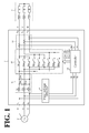
- FIG. 1 shows an exemplary configuration of a matrix converter according to an embodiment.
- a matrix converter 1 according to this embodiment is disposed between a three-phase AC power source 2 (hereinafter simply referred to as AC power source 2) and a load 3.
- AC power source 2 hereinafter simply referred to as AC power source 2
- An example of the load 3 is an AC motor.
- an R phase, an S phase, and a T phase of the AC power source 2 will be referred to as input phases
- a U phase, a V phase, and a W phase of the load 3 will be referred to as output phases.
- the matrix converter 1 includes input terminals Tr, Ys, and Tt, and output terminals Tu, Tv, and Tw.
- the R, S, and T phases of the AC power source 2 are respectively coupled to the input terminals Tr, Ts, and Tt.
- the U, V, and W phases of the load 3 are respectively coupled to the output terminals Tu, Tv, and Tw.
- the AC power source 2 supplies three-phase AC power to the matrix converter 1 through the input terminals Tr, Ts, and Tt.
- the matrix converter 1 converts the three-phase AC power into three-phase AC power of a desired voltage and a desired frequency. Then, the matrix converter 1 outputs the resulting three-phase AC power to the load 3 through the output terminals Tu, Tv, and Tw.
- the matrix converter 1 includes a power conversion section 10, an LC filter 11, an input voltage detection section 12, an output current detection section 13, and a control section 14.
- the power conversion section 10 includes a plurality of bidirectional switches, namely, Sru, Ssu, Stu, Srv, Ssv, Stv, Srw, Ssw, and Stw (hereinafter occasionally collectively referred to as bidirectional switch S).
- the plurality of bidirectional switches couple the phases of the AC power source 2 to the corresponding phases of the load 3.
- the bidirectional switches Sru, Ssu, and Stu respectively couple the R, S, and T phases of the AC power source 2 to the U phase of the load 3.
- the bidirectional switches Srv, Ssv, and Stv respectively couple the R, S, and T phases of the AC power source 2 to the V phase of the load 3.
- the bidirectional switches Srw, Ssw, and Stw respectively couple the R, S, and T phases of the AC power source 2 to the W phase of the load 3.
- the bidirectional switch S is made up of an anti-parallel connection of serial connection bodies each made up of a unidirectional switch and a diode.
- FIG. 2 shows an exemplary configuration of the bidirectional switch S.
- the bidirectional switch S includes a serial connection body 20 and a serial connection body 21.
- the serial connection body 20 is made up of a unidirectional switch Sio and a diode Dio
- the serial connection body 21 is made up of a unidirectional switch Soi and a diode Doi.
- the serial connection body 20 and the serial connection body 21 are anti-parallely connected to each other.
- unidirectional switches Sio and Soi include, but are not limited to, semiconductor switching elements such as metal-oxide-semiconductor field-effect transistor (MOSFET) and insulated gate bipolar transistor (IGBT).
- semiconductor switching elements such as metal-oxide-semiconductor field-effect transistor (MOSFET) and insulated gate bipolar transistor (IGBT).
- MOSFET metal-oxide-semiconductor field-effect transistor
- IGBT insulated gate bipolar transistor
- next generation semiconductor switching elements such as SiC and GaN.
- the bidirectional switch S will not be limited to the configuration shown in FIG. 2 .
- Another example of the bidirectional switch S is that the cathode of the diode Dio and the cathode of the diode Doi are not coupled to each other.
- the bidirectional switch S may not be provided with the diodes Dio and Doi, and the unidirectional switches Sio and Soi may be anti-parallely connected to each other.
- Reverse blocking IGBTs are a kind of IGBT that has a tolerance against reverse bias (a state where voltage is higher on the emitter side than on the collector side of IGBT).
- the LC filter 11 is disposed between the power conversion section 10 and the R, S, and T phases of the AC power source 2 to eliminate or minimize a flow of high frequency current from the power conversion section 10 to the AC power source 2.
- the LC filter 11 includes three reactors Lr, Ls, and Lt and three capacitors Crs, Cst, and Ctr, and removes high frequency components resulting from switching of the bidirectional switch S of the power conversion section 10.
- the input voltage detection section 12 detects voltage values Er, Es, and Et (hereinafter referred to as input phase voltages Er, Es, and Et) respectively of the R, S, and T phases of the AC power source 2.
- the input phase voltages Er, Es, and Et may be occasionally collectively referred to as input voltage Vi.
- inter-input phase voltages Ers, Est, and Etr may be occasionally collectively referred to as inter-input phase voltage Esa.
- the output current detection section 13 detects the current flowing between the power conversion section 10 and the load 3. Specifically, the output current detection section 13 detects instantaneous values Iu, Iv, and Iw (hereinafter referred to as output phase currents Iu, Iv, and Iw) of the currents flowing between the power conversion section 10 and the U, V, and W phases of the load 3.
- the output phase currents Iu, Iv, and Iw may be occasionally collectively referred to as output current Io.
- instantaneous values of the voltages respectively output to the U, V, and W phases of the load 3 from the power conversion section 10 may be occasionally referred to as output phase voltages Vu, Vv, and Vw.
- the output phase voltages Vu, Vv, and Vw may be occasionally collectively referred to as output voltage Vo.
- the control section 14 generates gate signals S1u to S6u, S1v to S6v, and S1w to S6w based on the input phase voltages Er, Es, and Et detected by the input voltage detection section 12 and based on the output phase currents Iu, Iv, and Iw detected by the output current detection section 13.
- the gate signals S1u to S6u, S1v to S6v, and S1w to S6w may be occasionally collectively referred to as gate signal Sg.
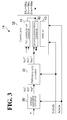
- FIG. 3 shows an exemplary configuration of the control section 14.
- the control section 14 includes a voltage command calculation section 30, a PWM duty ratio calculation section 31, and a commutation section 32.
- the control section 14 includes a microcomputer and various circuits.
- the microcomputer includes a central processing unit (CPU), a read only memory (ROM), a random access memory (RAM), and an input-output port.
- the CPU of the microcomputer reads and executes a program stored in the ROM to function as the voltage command calculation section 30, the PWM duty ratio calculation section 31, and the commutation section 32. It is possible to implement the control section 14 using hardware alone, without using any programs.
- the voltage command calculation section 30 Based on a frequency command f* and the output phase currents Iu, Iv, and Iw, the voltage command calculation section 30 generates voltage commands Vu*, Vv*, and Vw* (hereinafter occasionally collectively referred to as voltage command Vo*) for the respective output phases. Then, the voltage command calculation section 30 outputs the voltage commands Vu*, Vv*, and Vw*.
- the frequency command f* is a command associated with the frequencies of the output phase voltages Vu, Vv, and Vw.
- the PWM duty ratio calculation section 31 Based on the voltage commands Vu*, Vv*, and Vw* and based on the input phase voltages Er, Es, and Et, the PWM duty ratio calculation section 31 generates PWM voltage commands Vu1*, Vv1*, and Vw1*. It is possible to use any known technique to generate the PWM voltage commands Vu1*, Vv1*, and Vw1*. Exemplary techniques are described in Japanese Unexamined Patent Application Publication No. 2008-048550 and Japanese Unexamined Patent Application Publication No. 2012-239265 .
- the PWM duty ratio calculation section 31 makes the input phase voltages Er, Es, and Et into input phase voltages Ep, Em, and En in descending order. Then, the PWM duty ratio calculation section 31 converts the voltage commands Vu*, Vv*, and Vw* into pulse width modulation signals corresponding to the voltage values of the input phase voltages Ep, Em, and En. Then, the PWM duty ratio calculation section 31 outputs the resulting PWM voltage commands Vu1*, Vv1*, and Vw1*. In the following description, the PWM voltage commands Vu1*, Vv1*, and Vw1* may be occasionally collectively referred to as PWM voltage command Vo1*.
- the commutation section 32 executes commutation control, which is to switch the phases of the AC power source 2 to be coupled to the load 3 using the bidirectional switch S. Specifically, in response to the PWM voltage commands Vu1*, Vv1*, and Vw1*, the commutation section 32 determines the switching order of the bidirectional switch S at the time of commutation based on the polarity of each of the output phase currents Iu, Iv, and Iw and based on the input phase voltages Ep, Em, and En. Based on the switching order thus determined, the commutation section 32 generates the gate signals S1u to S6u, S1v to S6v, and S1w to S6w.
- the gate signals S1u to S6u, S1v to S6v, and S1w to S6w are input into each of the unidirectional switches Sio and Soi of the bidirectional switch S of the power conversion section 10.
- the unidirectional switches Sio and Soi are ON-OFF controlled.
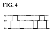
- FIG. 4 is a diagram illustrating switching among the input phase voltages Ep, Em, and En, which are output to the output phases.
- the bidirectional switch S is controlled by the gate signal Sg in the manner shown in FIG. 4 , where the input phase voltage output to each output phase switches in the order: En ⁇ Em ⁇ Ep ⁇ Em ⁇ En in a single cycle Tc of the PWM voltage command Vo1*, which is a pulse width modulation signal.
- the switching order of the input phase voltage to be output to the output phases is not limited to En ⁇ Em ⁇ Ep ⁇ Em ⁇ En.
- FIG. 5 illustrates a relationship between the unidirectional switches Sio and Soi of the plurality of bidirectional switches Sru, Ssu, Stu, Srv, Ssv, Stv, Srw, Ssw, and Stw and the gate signals S1u to S6u, S1v to S6v, and S1w to S6w.
- the LC filter 11 and the output current detection section 13 are omitted in FIG. 5 .
- the unidirectional switch Sio (see FIG. 2 ) of the bidirectional switch Sru is ON-OFF controlled by the gate signal S1u, and the unidirectional switch Soi (see FIG. 2 ) of the bidirectional switch Sru is controlled by the gate signal S2u.
- the unidirectional switch Sio of the bidirectional switch Ssu is ON-OFF controlled by the gate signal S3u, and the unidirectional switch Soi of the bidirectional switch Ssu is controlled by the gate signal S4u.
- the unidirectional switch Sio of the bidirectional switch Stu is ON-OFF controlled by the gate signal S5u, and the unidirectional switch Soi of the bidirectional switch Stu is controlled by the gate signal S6u.
- the unidirectional switches Sio and Soi of the bidirectional switches Srv, Ssv, and Stv are ON-OFF controlled by the gate signals S1v to S6v.
- the unidirectional switches Sio and Soi of the bidirectional switches Srw, Ssw, and Stw are ON-OFF controlled by the gate signals S1w to S6w.
- the commutation section 32 includes a first commutation control section 41, a second commutation control section 42, and a selection section 43.
- the first and second commutation control sections 41 and 42 are both capable of determining the switching order of the bidirectional switches and generating the gate signals S1u to S6u, S1v to S6v, and S1w to S6w.
- the selection section 43 selects one of the first and second commutation control sections 41 and 42 based on the states of the output phase currents Iu, Iv, and Iw. Then, the selection section 43 causes the selected commutation control section to output the gate signals S1u to S6u, S1v to S6v, and S1w to S6w. This improves the accuracy of the output voltage Vo.
- the configurations of the first commutation control section 41, the second commutation control section 42, and the selection section 43 will be described in detail below.
- the first commutation control section 41 performs the commutation control in a state where the conducting direction of the bidirectional switch S is unidirectional.
- a commutation method based on this commutation control such method will be hereinafter referred to as unidirectional switching commutation
- one of the unidirectional switches Sio and Soi of the bidirectional switch S is turned OFF, while the other one of the unidirectional switches is ON-OFF controlled.
- the unidirectional switching commutation shortens the time required for the commutation operation and improves voltage accuracy.
- Examples of the unidirectional switching commutation include 1-step current commutation and 2-step current commutation.
- the first commutation control section 41 by setting its inner parameters, is capable of using any one of the 1-step current commutation and the 2-step current commutation in performing the commutation control.
- the first commutation control section 41 generates the gate signals S1u to S6u, S1v to S6v, and S1w to S6w for performing the PWM control including the commutation operation that is based on the unidirectional switching commutation.
- each of the 1-step current commutation and the 2-step current commutation is similar throughout the U, V, and W phases, and the following description will take the U phase as an example. Also in the following description, the polarity of the output current Io flowing from the AC power source 2 to the load 3 will be regarded as positive (Io > 0).
- FIGs. 6A and 6B illustrate relationships in the 1-step current commutation between the output phase voltage Vu and the gate signals S1u to S6u.
- FIG. 6A illustrates the commutation operation in a case where the output phase current Iu is a positive value.
- FIG. 6B illustrates the commutation operation in a case where the output phase current Iu is a negative value.
- FIGs. 7A and 7B illustrate states of the unidirectional switches Sio and Soi at time t0 to time t5 shown in FIGs. 6A and 6B .
- Ep Er
- Em Es
- En Et.
- the gate signal S3u changes from Low level to High level.
- This state is as shown in FIG. 7A , where the unidirectional switch Sio is turned ON in the bidirectional switch Ssu serving as a switching destination.
- the conduction direction of the unidirectional switch Sio is the same as the direction of flow of the output phase current Iu.
- the input phase voltage output to the U phase is switched from En to Em, and continues to be output to the U phase.
- the unidirectional switch Soi is OFF, even though the unidirectional switch Soi has a conduction direction opposite to the direction of flow of the output phase current Iu. This ensures that no interphase short-circuiting of the AC power source 2 occurs.
- the gate signal S1u changes from Low level to High level.
- This state is as shown in FIG. 7A , where the unidirectional switch Sio is turned ON in the bidirectional switch Sru serving as the switching destination.
- the conduction direction of the unidirectional switch Sio is the same as the direction of flow of the output phase current Iu.
- the gate signal S1u changes from High level to Low level.
- This state is as shown in FIG. 7A , where the unidirectional switch Sio is turned OFF in the bidirectional switch Sru serving as the switching destination.
- the input phase voltage output to the U phase is switched to Em without interphase short-circuiting of the AC power source 2, and the input phase voltage continues to be output to the U phase.
- the gate signal S3u changes from High level to Low level.
- This state is as shown in FIG. 7A , where the unidirectional switch Sio is turned OFF in the bidirectional switch Ssu serving as the switching destination.
- the input phase voltage output to the U phase is switched to En without interphase short-circuiting of the AC power source 2, and the input phase voltage continues to be output to the U phase.
- the switching processing at time t1, time t2, time t4, and time t5 shown in FIG. 6B is similar to the switching processing at time t1, time t2, time t4, and time t5 shown in FIG. 6A .
- switching processing is performed with respect to the unidirectional switch Soi, which has the same conducting direction as the direction of flow of the output phase current Iu.
- the voltage to be output as the output phase voltage Vu is changeable in the order En ⁇ Em ⁇ Ep ⁇ Em ⁇ En.
- interphase short-circuiting of the AC power source 2 is eliminated or minimized, and opening of the output phase of the matrix converter 1 is eliminated or minimized.
- the input phase voltage output to the output phase is switchable on a one-step basis. This shortens the time required for the commutation operation and improves the voltage accuracy of the output phase.
- one unidirectional switch corresponding to the input phase voltage output to each output phase is turned ON, and also one unidirectional switch corresponding to the input phase voltage having an absolute value smaller than the input phase voltage output to each output phase is turned ON.
- the 1-step current commutation will not be limited to this switch control.
- FIGs. 8A and 8B Another possible example of 1-step current commutation is shown in FIGs. 8A and 8B .
- this 1-step current commutation only the one unidirectional switch corresponding to the input phase voltage output to each output phase is turned ON on a one-step basis.
- FIGs. 8A and 8B are diagrams respectively corresponding to FIGs. 6A and 6B , and illustrate relationships between the output phase voltage Vu and the gate signals S1u to S6u in the other 1-step current commutation.
- the unidirectional switching commutation includes the 2-step current commutation.
- the input phase voltage output to each output phase is switched in two steps 1 and 2.
- a unidirectional switch with a conducting direction that is the same as the direction of the output current Io is turned ON (step 1).
- a unidirectional switch with a conducting direction that is the same as the direction of the output current Io is turned OFF (step 2).
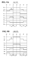
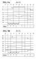
- FIGs. 9A and 9B illustrate the 2-step current commutation and respectively correspond to FIGs. 6A and 6B . Specifically, FIGs. 9A and 9B illustrate relationships between the output phase voltage Vu and the gate signals S1u to S6u in the 2-step current commutation.
- Each step has a time length of Td (hereinafter referred to as step time length Td).
- the step time length Td is longer than turn-ON time of the unidirectional switches Sio and Soi. While the steps have the same step time length Td for convenience of description, the steps may have mutually different step time lengths.
- the second commutation control section 42 performs the commutation control in a state where the conducing direction of the bidirectional switch S is bidirectional.
- a commutation method based on this commutation control such method will be hereinafter referred to as bidirectional switching commutation
- the unidirectional switches Sio and Soi of the bidirectional switches S serving as the switching source and destination are both ON controlled before and after the commutation operation.
- commutation failure refers to a state where interphase short-circuiting of the AC power source 2 occurs or the output phase goes into open state.
- Examples of the bidirectional switching commutation include 4-step voltage commutation, 3-step voltage commutation, 2-step voltage commutation, 4-step current commutation, 3-step current commutation, and 3-step voltage and current commutation.
- the second commutation control section 42 by setting its inner parameters, is capable of using any of the commutations in performing the commutation control.
- the second commutation control section 42 generates the gate signals S1u to S6u, S1v to S6v, and S1w to S6w for performing the PWM control including the commutation operation that is based on the bidirectional switching commutation.
- the 4-step voltage commutation is such a method of commutation that in order to eliminate or minimize inter-input phase short-circuiting and opening of the output phase, the ON-OFF order of the unidirectional switches Sio and Soi of the bidirectional switches S serving as the switching source and destination is determined based on a relationship in magnitude among the input phase voltages Er, Es, and Et.
- the commutation operation is based on a switching pattern of the following steps 1 to 4. In the 4-step voltage commutation, it is not necessary to change the switching pattern depending on the polarity of the output current Io.
- the reverse bias refers to a state where the input side voltage is lower than the output side voltage immediately before the commutation operation.
- the forward bias refers to a state where the input side voltage is higher than the output side voltage immediately before the commutation operation.
- the forward bias refers to a state where the input side voltage is lower than the output side voltage immediately before the commutation operation.
- the reverse bias refers to a state where the input side voltage is higher than the output side voltage immediately before the commutation operation.
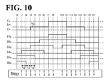
- FIG. 10 illustrates a relationship in the 4-step voltage commutation among the output phase voltage Vu, the gate signals S1u to S6u, and the steps in the commutation operation.
- FIG. 11 illustrates states of the unidirectional switches Sio and Soi at time t0 to time t17 shown in FIG. 10 .
- Ep Er
- Em Es
- En Et.
- the gate signal S4u changes from Low level to High level. This state is as shown in FIG. 11 , where the unidirectional switch Soi is turned ON in the bidirectional switch Ssu serving as the switching destination (step 1).
- the gate signal S6u changes from High level to Low level at time t2. This state is as shown in FIG. 11 , where the unidirectional switch Soi is turned OFF in the bidirectional switch Stu serving as the switching source (step 2).
- the gate signal S3u changes from Low level to High level. This state is as shown in FIG. 11 , where the unidirectional switch Soi is turned ON in the bidirectional switch Ssu (step 3).
- the gate signal S5u changes from High level to Low level. This state is as shown in FIG. 11 , where the unidirectional switch Sio is turned OFF in the bidirectional switch Stu (step 4).
- the switching processing at time t5 to time t8, time t10 to time t13, and time t14 to time t17 shown in FIG. 10 is similar to the switching processing of steps 1 to 4 at time t1 to time t4, as shown in FIG. 11 .
- the step time length Td is longer than the turn-ON time and turn-OFF time of the unidirectional switches Sio and Soi. While the steps have the same step time length Td for convenience of description, the steps may have mutually different step time lengths. This also applies in the commutations described below.
- the voltage to be output as the output phase voltage Vu is changeable in the order En ⁇ Em ⁇ Ep ⁇ Em ⁇ En.
- interphase short-circuiting of the AC power source 2 is eliminated or minimized, and opening of the output phase of the matrix converter 1 is eliminated or minimized.
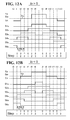
- the 3-step voltage commutation is a 3-step commutation that is based on a relationship in magnitude among the input phase voltages Er, Es, and Et and based on the polarity of the output current Io. This commutation operation is as shown in FIGs. 12A and 12B .
- FIGs. 12A and 12B illustrate a relationship in the 3-step voltage commutation between the output phase voltage Vu and the gate signals S1u to S6u, and correspond to FIG. 10 .
- FIG. 12A illustrates the commutation operation in a case where the output phase current Iu is a positive value.
- FIG. 12B illustrates the commutation operation in a case where the output phase current Iu is a negative value.
- the polarity of the output current Io is a positive value and the voltage output as the output phase voltage Vu is incremental.
- the commutation operation of the 3-step voltage commutation is based on a switching pattern of the following steps 1 to 3.
- the 2-step voltage commutation is such a method of commutation that the unidirectional switches Sio and Soi of the bidirectional switch S corresponding to the input phase voltage output to the output phase are both ON before and after the commutation operation, while in the remaining bidirectional switches S, only one of the unidirectional switches is ON.
- FIG. 13 illustrates a relationship in the 2-step voltage commutation between the output phase voltage Vu and the gate signals S1u to S6u, and corresponds to FIG. 10 .
- the step time length Td is longer than the turn-OFF time of the unidirectional switches Sio and Soi.
- the 2-step voltage commutation may be other than the commutation shown in FIG. 13 .
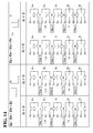
- Another example of the 2-step voltage commutation is shown in FIG. 14.
- FIG. 14 illustrates states of the unidirectional switches Sio and Soi in the other 2-step voltage commutation.
- the 2-step voltage commutation shown in FIG. 14 has different switch control patterns, which depend on the relationship in magnitude between EP - Em and Em-En and on the polarity of the output current Io.
- the step time length Td is longer than the turn-ON time and turn OFF time of the unidirectional switches Sio and Soi.
- a step time length Toff is longer than the turn-OFF time of the unidirectional switches Sio and Soi.
- the commutation operation is based on a switching pattern of the following steps 1 to 4 in accordance with the polarity of the output current Io.
- FIGs. 15A and 15B illustrate a relationship in the 4-step current commutation between the output phase voltage Vu and the gate signals S1u to S6u, and correspond to FIG. 10 .
- FIG. 15A illustrates the commutation operation in a case where the output phase current Iu is a positive value.
- FIG. 15B illustrates the commutation operation in a case where the output phase current Iu is a negative value.
- the voltage to be output as the output phase voltage Vu is changeable in the order En ⁇ Em ⁇ Ep ⁇ Em ⁇ En.
- interphase short-circuiting of the AC power source 2 is eliminated or minimized, and opening of the output phase of the matrix converter 1 is eliminated or minimized.
- the 3-step current commutation is a 3-step commutation that is based on the polarity of the output current Io.
- This commutation operation is as shown in FIGs. 16A and 16B.
- FIGs. 16A and 16B illustrate a relationship in the 3-step current commutation between the output phase voltage Vu and the gate signals S1u to S6u, and correspond to FIG. 10 .
- FIG. 16A illustrates the commutation operation in a case where the output phase current Iu is a positive value.
- FIG. 16B illustrates the commutation operation in a case where the output phase current Iu is a negative value.
- the commutation operation of the 3-step current commutation is based on a switching pattern of the following steps 1 to 3.
- the 3-step current commutation may be other than the above-described commutation control.
- Other examples of the 3-step current commutation are shown in FIGs. 17A and 17B , where steps 2 and 3 of a 4-step current commutation are simultaneously performed as a single step.
- FIGs. 17A and 17B illustrate a relationship in the 3-step current commutation between the output phase voltage Vu and the gate signals S1u to S6u, and correspond to FIG. 10 .
- FIG. 17A illustrates the commutation operation in a case where the output phase current Iu is a positive value.
- FIG. 17B illustrates the commutation operation in a case where the output phase current Iu is a negative value.
- the 3-step voltage and current commutation is such a method of commutation that one of its step 1 and step 2 is corresponding step 1 or step 2 of the 3-step voltage commutation, while the other one of step 1 and step 2 is corresponding step 1 or step 2 of the 3-step current commutation.
- FIGs. 18A and 18B illustrate a relationship in the 3-step voltage and current commutation between the output phase voltage Vu and the gate signals S1u to S6u, and correspond to FIG. 10 .
- FIG. 18A illustrates the commutation operation in a case where the output phase current Iu is a positive value.
- FIG. 18B illustrates the commutation operation in a case where the output phase current Iu is a negative value.
- the selection section 43 Based on the state of the output current Io of the power conversion section 10, the selection section 43 selects between the first commutation control section 41 and the second commutation control section 42 to perform the commutation control. As described above, the first commutation control section 41 performs the commutation control based on the unidirectional switching commutation, while the second commutation control section 42 performs the commutation control based on the bidirectional switching commutation.
- one unidirectional switch among the unidirectional switches Sio and Soi of the bidirectional switch S, that corresponds to the polarity of the output current Io is ON-OFF controlled. This shortens the time required for the commutation operation and improves voltage accuracy.
- one of the unidirectional switches Sio and Soi of the bidirectional switch S is ON before and after the commutation operation. If, however, the polarity of the output current Io is incorrect, no output current Io flows, and this no-flow state continues beyond the period without the commutation operation.
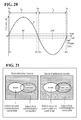
- FIG. 19A illustrates a region RA is where the output current Io is small and more susceptible to detection sensitivity and detection noise of the output current detection section 13. This leads to cases where no output current Io is output as exemplified in FIG. 19B.
- FIG. 19A illustrates a target waveform of the output current Io.
- FIG. 19B illustrates an output state of the output current Io caused by a commutation failure in the unidirectional switching commutation.
- the bidirectional switching commutation ensures that a resulting commutation failure, if any, is only within the commutation operation period, eliminating or minimizing such occurrences as opening of the output phase and inter-input phase short-circuiting outside the commutation operation period.
- the 4-step voltage commutation even if the polarity of the output current Io is incorrect, no commutation failure occurs.
- the bidirectional switching commutation eliminates or minimizes those situations in which no output current Io is output.
- the bidirectional switching commutation has a larger number of steps than the unidirectional switching commutation does. This elongates the time required for the commutation operation, resulting in degraded voltage accuracy compared with the unidirectional switching commutation. This necessitates voltage compensation processing or similar processing, which makes the bidirectional switching commutation complex.
- the selection section 43 selects between the first commutation control section 41 and the second commutation control section 42 to perform the commutation control. This ensures that the commutation control is based on a suitable commutation method selected between the unidirectional switching commutation and the bidirectional switching. This, in turn, eliminates or minimizes a commutation failure while improving accuracy of the output voltage Vo.
- the selection section 43 has first selection mode and second selection mode for the commutation control section.
- the selection section 43 by setting its inner parameters, is capable of selecting the commutation control section in any one of first selection mode and second selection mode.
- FIG. 20 illustrates a relationship between the output current Io and the commutation control section selected in first selection mode.
- the selection section 43 selects the first commutation control section 41 in period Ta, during which the output current Io is equal to or larger than a current threshold Iref.
- the selection section 43 selects the second commutation control section 42.
- the current threshold Iref is the same throughout the case where the output current Io is a positive value and the case where the output current Io is a negative value.
- the current threshold Iref may also vary between the case where the output current Io is a positive value and the case where the output current Io is a negative value.
- the second selection mode is different from the first selection mode in that the first commutation control section 41 is selected even when the output current Io is smaller than the current threshold Iref, insofar as the inter-input phase voltage Esa is smaller than a voltage threshold Eref.
- FIG. 21 illustrates a difference between first selection mode and second selection mode.
- first selection mode the prevention of opening of the output phase is prioritized over the prevention of the inter-input phase short-circuiting.
- second selection mode the prevention of inter-input phase short-circuiting is prioritized over the prevention of opening of the output phase.
- the bidirectional switching commutation that the second commutation control section 42 uses in the second selection mode eliminates or minimizes inter-input phase short-circuiting.
- Examples of the bidirectional switching commutation that the second commutation control section 42 uses in the second selection mode include the 4-step current commutation shown in FIG. 15A and other drawings, and the 2-step current commutation shown in FIG. 14 .
- the selection section 43 selects the first commutation control section 41 when the output current Io is equal to or larger than the current threshold Iref, or when the output current Io is smaller than the current threshold Iref and the inter-input phase voltage Esa is smaller than a voltage threshold Eref.
- the selection section 43 selects the second commutation control section 42 when the output current Io is smaller than the current threshold Iref and the inter-input phase voltage Esa is equal to or larger than the voltage threshold Eref.
- the current threshold Iref and the voltage threshold Eref each may vary between the case where the output current Io is a positive value and the case where the output current Io is a negative value.
- FIG. 22 illustrates a configuration of the selection section 43.
- the selection section 43 includes a U-phase selection section 50A, a V-phase selection section 50B, and a W-phase selection section 50C.
- the U-phase selection section 50A selects one of the first and second commutation control sections 41 and 42 based on the magnitude of the output phase current Iu, and outputs the gate signals S1u to S6u output from the selected commutation control section.
- the V-phase selection section 50B selects one of the first and second commutation control sections 41 and 42 based on the magnitude of the output phase current Iv, and outputs the gate signals S1v to S6v output from the selected commutation control section.
- the W-phase selection section 50C selects one of the first and second commutation control sections 41 and 42 based on the magnitude of the output phase current Iw, and outputs the gate signals S1w to S6w output from the selected commutation control section.
- a configuration of the U-phase selection section 50A will be described in detail below.
- the configurations of the V-phase selection section 50B and W-phase selection section 50C are the same as the configuration of the U-phase selection section 50A, and thus will not be described.
- the U-phase selection section 50A includes absolute-value calculation sections 51 and 55, a current threshold output section 52, subtraction sections 53 and 57, switch sections 54 and 59, a voltage threshold output section 56, and a selected mode output section 58.
- the absolute-value calculation section 51 calculates an absolute value Iua of the output phase current Iu to obtain the magnitude of the output phase current Iu, and outputs the absolute value Iua to the subtraction section 53.
- the current threshold output section 52 outputs the current threshold Iref, which is set in advance, to the subtraction section 53.
- the subtraction section 53 subtracts the current threshold Iref from the absolute value Iua, and outputs a difference Idif to the switch section 54.
- the switch section 54 receives the gate signals S1u to S6u from each of the first and second commutation control sections 41 and 42, and outputs the gate signals S1u to S6u from one of the commutation control sections based on the difference Idif output from the subtraction section 53. Specifically, when the difference Idif is 0 or a positive value, the switch section 54 selects and outputs the gate signals S1u to S6u output from the first commutation control section 41. When the difference Idif is a negative value, the switch section 54 selects and outputs the gate signals S1u to S6u output from the second commutation control section 42.
- the absolute-value calculation section 55 receives the input phase voltages Er, Es, and Et, and obtains absolute values of the inter-input phase voltages Ers, Est, and Etr from the input phase voltages Er, Es, and Et.
- the inter-input phase voltage Ers is a voltage between the R and S phases.
- the inter-input phase voltage Est is a voltage between the S and T phases.
- the inter-input phase voltage Etr is a voltage between the T and R phases.
- the voltage threshold output section 56 calculates the absolute values Ersa, Esta, and Etra respectively of the inter-input phase voltages Ers, Est, and Etr to obtain the magnitudes of the inter-input phase voltages Ers, Est, and Etr, and outputs the absolute values Ersa, Esta, and Etra to the subtraction section 53.
- the voltage threshold output section 56 outputs the voltage threshold Eref, which is set in advance, to the subtraction section 57.
- the subtraction section 57 subtracts the voltage threshold Eref from each of the inter-input phase voltages Ers, Est, and Etr, and outputs differences Ersdif, Estdif, and Etrdif to the switch section 59.
- the selected mode output section 58 outputs mode information to the switch section 59.
- the mode information indicates which of the selection mode, first selection mode or second selection mode, is set as a parameter.
- the switch section 59 receives the output from the switch section 54 and the output from the first commutation control section 41. Then, based on the differences from the subtraction section 57 and based on the mode information from the selected mode output section 58, the switch section 59 selects and outputs one of the outputs from the switch section 54 and the first commutation control section 41.
- the switch section 59 selects and outputs the output from the switch section 54. Then, when the output current Io is equal to or larger than the current threshold Iref, the gate signal Sg from the first commutation control section 41 is output. When the output current Io is smaller than the current threshold Iref, the gate signal Sg from the second commutation control section 42 is output.
- the switch section 59 selects and outputs the output from the switch section 54 or the output from the first commutation control section 41 based on the differences from the subtraction section 57.
- the switch section 59 selects and outputs the gate signals S1u to S6u output from the switch section 54 when the difference Estdif is 0 or a positive value.
- the switch section 59 selects and outputs the gate signals S1u to S6u output from the first commutation control section 41.
- the switch section 59 selects and outputs the gate signals S1u to S6u output from the switch section 54 when the difference Ersdif is 0 or a positive value.
- the switch section 59 selects and outputs the gate signals S1u to S6u output from the first commutation control section 41.
- the selection section 43 selects between the first commutation control section 41 and the second commutation control section 42 to perform the commutation control. This enables the matrix converter 1 to eliminate or minimize a commutation failure while improving the accuracy of the output voltage Vo.
- FIG. 23 illustrates another configuration of the U-phase selection section 50A in the selection section 43.
- the configurations of the V-phase selection section 50B and the W-phase selection section 50C are the same as the configuration of the U-phase selection section 50A.
- the U-phase selection section 50A includes phase calculation sections 51A and 55A, phase threshold output sections 52A and 56A, and comparison sections 53A and 57A, instead of the absolute-value calculation sections 51 and 55, the current threshold output section 52, the voltage threshold output section 56, and the subtraction sections 53 and 57 shown in FIG. 22 .
- the U-phase selection section 50A is otherwise similar to the configuration shown in FIG. 22 .
- the phase calculation section 51A receives the output phase current Iu to obtain a phase ⁇ u of the output phase current Iu.
- the phase calculation section 51A may also obtain the phase ⁇ u of the output phase current Iu from any one of the output phase currents Iv and Iw.
- the phase threshold output section 52A outputs a phase threshold ⁇ oref. Examples of the range of the phase threshold ⁇ oref are shown in FIG. 20 : “0° to ⁇ 1 ", " ⁇ 2 to ⁇ 3 ", and " ⁇ 4 to 360°”.
- the comparison section 53A compares the phase ⁇ u of the output phase current Iu output from the phase calculation section 51A with the phase threshold ⁇ oref output from the phase threshold output section 52A. When the phase ⁇ u is contained in the phase threshold ⁇ oref, the comparison section 53A outputs a negative signal. When the phase ⁇ u is not contained in the phase threshold ⁇ oref, the comparison section 53A outputs a positive signal.
- the phase calculation section 55A receives the input phase voltages Er, Es, and Et to obtain a phase ⁇ i of the input voltage Vi.
- the phase calculation section 55A may also obtain the phase ⁇ i of the input voltage Vi from any one of the input phase voltages Er, Es, and Et.
- the phase threshold output section 56A outputs phase thresholds ⁇ rsref, ⁇ stref, and ⁇ trref respectively for the inter-input phase voltages Ers, Est, and Etr.
- the phase threshold ⁇ rsref is set within such an example range of the phase ⁇ i that the absolute value of the inter-input phase voltage Ers is equal to or smaller than the voltage threshold Eref.
- the phase threshold ⁇ stref is set within such an example range of the phase ⁇ i that the absolute value of the inter-input phase voltage Est is equal to or smaller than the voltage threshold Eref.
- the phase threshold ⁇ trref is set within such an example range of the phase ⁇ i that the absolute value of the inter-input phase voltage Etr is equal to or smaller than the voltage threshold Eref.
- the comparison section 57A compares the phase ⁇ i of the input voltage Vi output from the phase calculation section 55A with each of the thresholds ⁇ rsref, ⁇ stref, and ⁇ trref output from the phase threshold output section 56A.
- the comparison section 57A outputs a negative signal associated with the inter-input phase voltage Ers.
- the comparison section 57A outputs a positive signal associated with the inter-input phase voltage Ers.
- the comparison section 57A When the phase ⁇ i is contained in the phase threshold ⁇ stref, the comparison section 57A outputs a negative signal associated with the inter-input phase voltage Est. When the phase ⁇ i is not contained in the phase threshold ⁇ stref, the comparison section 57A outputs a positive signal associated with the inter-input phase voltage Est. When the phase ⁇ i is contained in the phase threshold ⁇ trref, the comparison section 57A outputs a negative signal associated with the inter-input phase voltage Etr. When the phase ⁇ i is not contained in the phase threshold ⁇ trref, the comparison section 57A outputs a positive signal associated with the inter-input phase voltage Etr.
- the switch section 59 selects and outputs the gate signals S1u to S6u output from the switch section 54 when the positive signal associated with the inter-input phase voltage Ers is output from the comparison section 57A.
- the switch section 59 selects and outputs the gate signals S1u to S6u output from the first commutation control section 41.
- the switch section 59 makes a selection based on signals associated with the inter-input phase voltage Est.
- the switch section 59 makes a selection based on signals associated with the inter-input phase voltage Etr.
- the selection section 43 is capable of selecting between the first commutation control section 41 and the second commutation control section 42 to perform the commutation control based on the phase of the output current Io and the phase of the input voltage Vi.
- the selection section 43 will not be limited to the above-described configuration.
- the phase selection sections 50A to 50C obtain the phase ⁇ o of the output current Io for the state of the output current Io, while for the state of the inter-input phase voltage Esa, the phase selection sections 50A to 50C obtain the inter-input phase voltage Esa.
- the phase selection sections 50A to 50C may obtain the phase ⁇ o of the output current Io at the phase calculation section 51A, the phase threshold output section 52A, and the comparison section 53A. Then, at the absolute-value calculation section 55, the voltage threshold output section 56, and the subtraction section 57, the phase selection sections 50A to 50C may obtain the magnitude of the inter-input phase voltage Esa.
- the phase selection sections 50A to 50C may also obtain the magnitude of the output current Io for the state of the output current Io, and obtain the phase ⁇ i of the input voltage Vi for the state of the inter-input phase voltage Esa.
- the phase selection sections 50A to 50C each may obtain the magnitude of the output current Io at the absolute-value calculation section 51, the current threshold output section 52, and the subtraction section 53, and obtain the phase ⁇ i of the input voltage Vi at the phase calculation section 55A, the phase threshold output section 56A and the comparison section 57A.
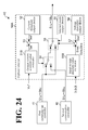
- the selection section 43 has been described as determining the states of the inter-input phase voltage Esa and the output current Io based on a detected value. As shown in FIG. 24 , it is also possible to use an input voltage estimation section to estimate the state of the inter-input phase voltage Esa, and use an output current estimation section to estimate the state of the output current Io.
- FIG. 24 illustrates a still another configuration of the U-phase selection section 50A in the selection section 43.
- the configurations of the V-phase selection section 50B and the W-phase selection section 50C are the same as the configuration of the U-phase selection section 50A.
- the U-phase selection section 50A includes an output current absolute-value estimation section 51B and an input voltage absolute-value estimation section 55B, instead of the absolute-value calculation sections 51 and 55 shown in FIG. 22 .
- the U-phase selection section 50A is otherwise similar to the configuration shown in FIG. 22 .
- the output current absolute-value estimation section 51B obtains the absolute value Iua of the output phase current Iu from the voltage command Vo*.
- the output current absolute-value estimation section 51B includes a table or a formula indicating the relationship between the voltage command Vu* and the absolute value Iua of the output phase current Iu. Based on the table or the formula, the output current absolute-value estimation section 51B obtains the absolute value Iua of the output phase current Iu.
- the input voltage absolute-value estimation section 55B estimates the absolute values Ersa, Esta, and Etra of the inter-input phase voltages Ers, Est, and Etr based on an input current Ii output from an input current estimation section (not shown).
- the input voltage absolute-value estimation section 55B includes a table or a formula indicating the relationship between the input phase current Ir and the absolute value of the input phase voltage Er. Based on the table or the formula, the input voltage absolute-value estimation section 55B obtains the absolute values Ersa, Esta, and Etra of the inter-input phase voltages Ers, Est, and Etr.
- the matrix converter 1 determines the state of the inter-input phase voltage Esa and the state of the output current Io based on a detected value or an estimated value. Then, the matrix converter 1 selects between the first commutation control section 41 and the second commutation control section 42 to perform the commutation control. This enables the matrix converter 1 to eliminate or minimize a commutation failure while improving the accuracy of the output voltage Vo.
Landscapes
- Engineering & Computer Science (AREA)
- Power Engineering (AREA)
- Ac-Ac Conversion (AREA)
Abstract
Description
- The present invention relates to a matrix converter.
- Matrix converters include a plurality of bidirectional switches that couple between an AC (alternating-current) power source and a load. The bidirectional switches are controlled to directly switch phase voltages of the AC power source so as to output a desired voltage and a desired frequency to the load.
- The matrix converters perform commutation, which is to switch between the phases of the AC power source to be coupled to the load using a bidirectional switch. Marcus Ziegler and Wilfried Hofmann propose a method of commutation in "Rectifier based robust control of bidirectional switches in AC-AC matrix converters" (EPE-PEMC 2002 Dubrovnik & Cavtat). Specifically, a bidirectional switch is switched with its conducting direction being unidirectional depending on the polarity of the output current.
- The contents of "Rectifier based robust control of bidirectional switches in AC-AC matrix converters" are incorporated herein by reference in their entirety.
- The proposed method of commutation shortens the time required for the commutation and thus improves voltage accuracy. However, there is dependency on the detection accuracy of the polarity of the output current. That is, a normal commutation may not be possible depending on the detection accuracy of the polarity of the output current, resulting in degraded accuracy of the output voltage.
- One aspect of an embodiment has been made in view of the above-described circumstances, and it is an object of the present disclosure to provide a matrix converter capable of improving accuracy of output voltage.
- According to one aspect of the present disclosure, a matrix converter includes a power conversion section and a control section. The power conversion section includes a plurality of bidirectional switches each having a controllable conducting direction. The bidirectional switches are disposed between a plurality of input terminals and a plurality of output terminals. The plurality of input terminals are respectively coupled to phases of an AC power source. The plurality of output terminals are respectively coupled to phases of a load. The control section is configured to control the plurality of bidirectional switches. The control section includes a first commutation control section, a second commutation control section, and a selection section. The first commutation control section is configured to perform commutation control in a state where the conducting direction of the bidirectional switches is unidirectional. The second commutation control section is configured to perform the commutation control in a state where the conducting direction of the bidirectional switches is bidirectional. The selection section is configured to select between the first commutation control section and the second commutation control section to perform the commutation control based on a state of an output current from the power conversion section.
- The one aspect of the embodiment provides a matrix converter capable of improving accuracy of output voltage.
- A more complete appreciation of the present disclosure and many of the attendant advantages thereof will be readily obtained as the same becomes better understood by reference to the following detailed description when considered in connection with the accompanying drawings, wherein:
-
FIG. 1 is a diagram illustrating an exemplary configuration of a matrix converter according to an embodiment; -
FIG. 2 is a diagram illustrating an exemplary configuration of a bidirectional switch shown inFIG. 1 ; -
FIG. 3 is a diagram illustrating an exemplary configuration of a control section shown inFIG. 1 ; -
FIG. 4 is a diagram illustrating switching among input phase voltages output to output phases; -
FIG. 5 illustrates a relationship between unidirectional switches of a plurality of bidirectional switches and gate signals; -
FIG. 6A illustrates a relationship between an output phase voltage and gate signals in a case where an output phase current is a positive value in a 1-step current commutation; -
FIG. 6B illustrates a relationship between the output phase voltage and the gate signals in a case where the output phase current is a negative value in the 1-step current commutation; -
FIG. 7A illustrates states of the unidirectional switch in the 1-step current commutation shown inFIG. 6A ; -
FIG. 7B illustrates a state of the unidirectional switch in the 1-step current commutation shown inFIG. 6B ; -
FIG. 8A illustrates a relationship between the output phase voltage and the gate signals in a case where the output phase current is a positive value in another 1-step current commutation; -
FIG. 8B illustrates a relationship between the output phase voltage and the gate signals in a case where the output phase current is a negative value in the other 1-step current commutation; -
FIG. 9A illustrates a relationship between the output phase voltage and the gate signals in a case where the output phase current is a positive value in a 2-step current commutation; -
FIG. 9B illustrates a relationship between the output phase voltage and the gate signals in a case where the output phase current is a negative value in the 2-step current commutation; -
FIG. 10 illustrates a relationship among an output phase voltage, the gate signals, and steps in a commutation operation in a 4-step voltage commutation; -
FIG. 11 illustrates a state of the unidirectional switches in the 4-step voltage commutation shown inFIG. 10 ; -
FIG. 12A illustrates a relationship between the output phase voltage and the gate signals in a case where the output phase current is a positive value in a 3-step voltage commutation; -
FIG. 12B illustrates a relationship between the output phase voltage and the gate signals in a case where the output phase current is a negative value in the 3-step voltage commutation; -
FIG. 13 illustrates a relationship among the output phase voltage, the gate signals, and steps in a commutation operation in a 2-step voltage commutation; -
FIG. 14 illustrates states of the unidirectional switches in another 2-step voltage commutation; -
FIG. 15A illustrates a relationship between the output phase voltage and the gate signals in a case where the output phase current is a positive value in a 4-step current commutation; -
FIG. 15B illustrates a relationship between the output phase voltage and the gate signals in a case where the output phase current is a negative value in the 4-step current commutation; -
FIG. 16A illustrates a relationship between the output phase voltage and the gate signals in a case where the output phase current is a positive value in a 3-step current commutation; -
FIG. 16B illustrates a relationship between the output phase voltage and the gate signals in a case where the output phase current is a negative value in the 3-step current commutation; -
FIG. 17A illustrates a relationship between the output phase voltage and the gate signals in a case where the output phase current is a positive value in another 3-step current commutation; -
FIG. 17B illustrates a relationship between the output phase voltage and the gate signals in a case where the output phase current is a negative value in the other 3-step current commutation; -
FIG. 18A illustrates a relationship between the output phase voltage and the gate signals in a case where the output phase current is a positive value in a 3-step voltage and current commutation; -
FIG. 18B illustrates a relationship between the output phase voltage and the gate signals in a case where the output phase current is a negative value in the 3-step voltage and current commutation; -
FIG. 19A illustrates a target waveform of the output current; -
FIG. 19B illustrates an output state of the output current caused by a commutation failure in an unidirectional switching commutation; -
FIG. 20 illustrates a relationship between a commutation control section selected in first selection mode and the output current; -
FIG. 21 illustrates a difference between first selection mode and second selection mode; -
FIG. 22 is a diagram illustrating a configuration of a selection section shown inFIG. 3 ; -
FIG. 23 is a diagram illustrating another configuration of the selection section shown inFIG. 3 ; and -
FIG. 24 is a diagram illustrating a still another configuration of the selection section shown inFIG. 3 . - The embodiments will now be described with reference to the accompanying drawings, wherein like reference numerals designate corresponding or identical elements throughout the various drawings.
-
FIG. 1 shows an exemplary configuration of a matrix converter according to an embodiment. As shown inFIG. 1 , amatrix converter 1 according to this embodiment is disposed between a three-phase AC power source 2 (hereinafter simply referred to as AC power source 2) and aload 3. An example of theload 3 is an AC motor. In the following description, an R phase, an S phase, and a T phase of theAC power source 2 will be referred to as input phases, while a U phase, a V phase, and a W phase of theload 3 will be referred to as output phases. - The
matrix converter 1 includes input terminals Tr, Ys, and Tt, and output terminals Tu, Tv, and Tw. The R, S, and T phases of theAC power source 2 are respectively coupled to the input terminals Tr, Ts, and Tt. The U, V, and W phases of theload 3 are respectively coupled to the output terminals Tu, Tv, and Tw. TheAC power source 2 supplies three-phase AC power to thematrix converter 1 through the input terminals Tr, Ts, and Tt. Thematrix converter 1 converts the three-phase AC power into three-phase AC power of a desired voltage and a desired frequency. Then, thematrix converter 1 outputs the resulting three-phase AC power to theload 3 through the output terminals Tu, Tv, and Tw. - As shown in
FIG. 1 , thematrix converter 1 includes apower conversion section 10, anLC filter 11, an inputvoltage detection section 12, an outputcurrent detection section 13, and acontrol section 14. - The
power conversion section 10 includes a plurality of bidirectional switches, namely, Sru, Ssu, Stu, Srv, Ssv, Stv, Srw, Ssw, and Stw (hereinafter occasionally collectively referred to as bidirectional switch S). The plurality of bidirectional switches couple the phases of theAC power source 2 to the corresponding phases of theload 3. - The bidirectional switches Sru, Ssu, and Stu respectively couple the R, S, and T phases of the
AC power source 2 to the U phase of theload 3. The bidirectional switches Srv, Ssv, and Stv respectively couple the R, S, and T phases of theAC power source 2 to the V phase of theload 3. The bidirectional switches Srw, Ssw, and Stw respectively couple the R, S, and T phases of theAC power source 2 to the W phase of theload 3. - The bidirectional switch S is made up of an anti-parallel connection of serial connection bodies each made up of a unidirectional switch and a diode.
FIG. 2 shows an exemplary configuration of the bidirectional switch S. As shown inFIG. 2 , the bidirectional switch S includes aserial connection body 20 and aserial connection body 21. Theserial connection body 20 is made up of a unidirectional switch Sio and a diode Dio, and theserial connection body 21 is made up of a unidirectional switch Soi and a diode Doi. Theserial connection body 20 and theserial connection body 21 are anti-parallely connected to each other. - Examples of the unidirectional switches Sio and Soi include, but are not limited to, semiconductor switching elements such as metal-oxide-semiconductor field-effect transistor (MOSFET) and insulated gate bipolar transistor (IGBT). Other examples include next generation semiconductor switching elements such as SiC and GaN.
- The bidirectional switch S will not be limited to the configuration shown in
FIG. 2 . Another example of the bidirectional switch S is that the cathode of the diode Dio and the cathode of the diode Doi are not coupled to each other. When the unidirectional switches Sio and Soi are reverse blocking IGBTs, the bidirectional switch S may not be provided with the diodes Dio and Doi, and the unidirectional switches Sio and Soi may be anti-parallely connected to each other. Reverse blocking IGBTs are a kind of IGBT that has a tolerance against reverse bias (a state where voltage is higher on the emitter side than on the collector side of IGBT). - The
LC filter 11 is disposed between thepower conversion section 10 and the R, S, and T phases of theAC power source 2 to eliminate or minimize a flow of high frequency current from thepower conversion section 10 to theAC power source 2. Specifically, theLC filter 11 includes three reactors Lr, Ls, and Lt and three capacitors Crs, Cst, and Ctr, and removes high frequency components resulting from switching of the bidirectional switch S of thepower conversion section 10. - The input
voltage detection section 12 detects voltage values Er, Es, and Et (hereinafter referred to as input phase voltages Er, Es, and Et) respectively of the R, S, and T phases of theAC power source 2. In the following description, the input phase voltages Er, Es, and Et may be occasionally collectively referred to as input voltage Vi. Also, inter-input phase voltages Ers, Est, and Etr may be occasionally collectively referred to as inter-input phase voltage Esa. Here, the following applies: Ers = Er - Es, Est = Es - Et, and Etr = Et-Er. - The output
current detection section 13 detects the current flowing between thepower conversion section 10 and theload 3. Specifically, the outputcurrent detection section 13 detects instantaneous values Iu, Iv, and Iw (hereinafter referred to as output phase currents Iu, Iv, and Iw) of the currents flowing between thepower conversion section 10 and the U, V, and W phases of theload 3. In the following description, the output phase currents Iu, Iv, and Iw may be occasionally collectively referred to as output current Io. Also, instantaneous values of the voltages respectively output to the U, V, and W phases of theload 3 from thepower conversion section 10 may be occasionally referred to as output phase voltages Vu, Vv, and Vw. The output phase voltages Vu, Vv, and Vw may be occasionally collectively referred to as output voltage Vo. - The
control section 14 generates gate signals S1u to S6u, S1v to S6v, and S1w to S6w based on the input phase voltages Er, Es, and Et detected by the inputvoltage detection section 12 and based on the output phase currents Iu, Iv, and Iw detected by the outputcurrent detection section 13. In the following description, the gate signals S1u to S6u, S1v to S6v, and S1w to S6w may be occasionally collectively referred to as gate signal Sg. -
FIG. 3 shows an exemplary configuration of thecontrol section 14. As shown inFIG. 3 , thecontrol section 14 includes a voltagecommand calculation section 30, a PWM dutyratio calculation section 31, and acommutation section 32. Thecontrol section 14 includes a microcomputer and various circuits. The microcomputer includes a central processing unit (CPU), a read only memory (ROM), a random access memory (RAM), and an input-output port. The CPU of the microcomputer reads and executes a program stored in the ROM to function as the voltagecommand calculation section 30, the PWM dutyratio calculation section 31, and thecommutation section 32. It is possible to implement thecontrol section 14 using hardware alone, without using any programs. - Based on a frequency command f* and the output phase currents Iu, Iv, and Iw, the voltage
command calculation section 30 generates voltage commands Vu*, Vv*, and Vw* (hereinafter occasionally collectively referred to as voltage command Vo*) for the respective output phases. Then, the voltagecommand calculation section 30 outputs the voltage commands Vu*, Vv*, and Vw*. The frequency command f* is a command associated with the frequencies of the output phase voltages Vu, Vv, and Vw. - Based on the voltage commands Vu*, Vv*, and Vw* and based on the input phase voltages Er, Es, and Et, the PWM duty
ratio calculation section 31 generates PWM voltage commands Vu1*, Vv1*, and Vw1*. It is possible to use any known technique to generate the PWM voltage commands Vu1*, Vv1*, and Vw1*. Exemplary techniques are described in Japanese Unexamined Patent Application Publication No.2008-048550 2012-239265 - For example, during a period of unchanging relationship in magnitude among the input phase voltages Er, Es, and Et, the PWM duty
ratio calculation section 31 makes the input phase voltages Er, Es, and Et into input phase voltages Ep, Em, and En in descending order. Then, the PWM dutyratio calculation section 31 converts the voltage commands Vu*, Vv*, and Vw* into pulse width modulation signals corresponding to the voltage values of the input phase voltages Ep, Em, and En. Then, the PWM dutyratio calculation section 31 outputs the resulting PWM voltage commands Vu1*, Vv1*, and Vw1*. In the following description, the PWM voltage commands Vu1*, Vv1*, and Vw1* may be occasionally collectively referred to as PWM voltage command Vo1*. - The
commutation section 32 executes commutation control, which is to switch the phases of theAC power source 2 to be coupled to theload 3 using the bidirectional switch S. Specifically, in response to the PWM voltage commands Vu1*, Vv1*, and Vw1*, thecommutation section 32 determines the switching order of the bidirectional switch S at the time of commutation based on the polarity of each of the output phase currents Iu, Iv, and Iw and based on the input phase voltages Ep, Em, and En. Based on the switching order thus determined, thecommutation section 32 generates the gate signals S1u to S6u, S1v to S6v, and S1w to S6w. - The gate signals S1u to S6u, S1v to S6v, and S1w to S6w are input into each of the unidirectional switches Sio and Soi of the bidirectional switch S of the
power conversion section 10. Thus, the unidirectional switches Sio and Soi are ON-OFF controlled. -
FIG. 4 is a diagram illustrating switching among the input phase voltages Ep, Em, and En, which are output to the output phases. The bidirectional switch S is controlled by the gate signal Sg in the manner shown inFIG. 4 , where the input phase voltage output to each output phase switches in the order: En → Em → Ep → Em → En in a single cycle Tc of the PWM voltage command Vo1*, which is a pulse width modulation signal. The switching order of the input phase voltage to be output to the output phases is not limited to En → Em → Ep → Em → En. -
FIG. 5 illustrates a relationship between the unidirectional switches Sio and Soi of the plurality of bidirectional switches Sru, Ssu, Stu, Srv, Ssv, Stv, Srw, Ssw, and Stw and the gate signals S1u to S6u, S1v to S6v, and S1w to S6w. TheLC filter 11 and the outputcurrent detection section 13 are omitted inFIG. 5 . - The unidirectional switch Sio (see
FIG. 2 ) of the bidirectional switch Sru is ON-OFF controlled by the gate signal S1u, and the unidirectional switch Soi (seeFIG. 2 ) of the bidirectional switch Sru is controlled by the gate signal S2u. The unidirectional switch Sio of the bidirectional switch Ssu is ON-OFF controlled by the gate signal S3u, and the unidirectional switch Soi of the bidirectional switch Ssu is controlled by the gate signal S4u. The unidirectional switch Sio of the bidirectional switch Stu is ON-OFF controlled by the gate signal S5u, and the unidirectional switch Soi of the bidirectional switch Stu is controlled by the gate signal S6u. - Similarly, the unidirectional switches Sio and Soi of the bidirectional switches Srv, Ssv, and Stv are ON-OFF controlled by the gate signals S1v to S6v. The unidirectional switches Sio and Soi of the bidirectional switches Srw, Ssw, and Stw are ON-OFF controlled by the gate signals S1w to S6w.
- Referring back to
FIG. 3 , thecontrol section 14 will be further described. Thecommutation section 32 includes a firstcommutation control section 41, a secondcommutation control section 42, and aselection section 43. The first and secondcommutation control sections - The
selection section 43 selects one of the first and secondcommutation control sections selection section 43 causes the selected commutation control section to output the gate signals S1u to S6u, S1v to S6v, and S1w to S6w. This improves the accuracy of the output voltage Vo. The configurations of the firstcommutation control section 41, the secondcommutation control section 42, and theselection section 43 will be described in detail below. - The first
commutation control section 41 performs the commutation control in a state where the conducting direction of the bidirectional switch S is unidirectional. In a commutation method based on this commutation control (such method will be hereinafter referred to as unidirectional switching commutation), one of the unidirectional switches Sio and Soi of the bidirectional switch S is turned OFF, while the other one of the unidirectional switches is ON-OFF controlled. Thus, the unidirectional switching commutation shortens the time required for the commutation operation and improves voltage accuracy. - Examples of the unidirectional switching commutation include 1-step current commutation and 2-step current commutation. The first
commutation control section 41, by setting its inner parameters, is capable of using any one of the 1-step current commutation and the 2-step current commutation in performing the commutation control. The firstcommutation control section 41 generates the gate signals S1u to S6u, S1v to S6v, and S1w to S6w for performing the PWM control including the commutation operation that is based on the unidirectional switching commutation. - First, the 1-step current commutation will be described by referring to
FIGs. 6A, 6B ,7A, and 7B . Here, each of the 1-step current commutation and the 2-step current commutation is similar throughout the U, V, and W phases, and the following description will take the U phase as an example. Also in the following description, the polarity of the output current Io flowing from theAC power source 2 to theload 3 will be regarded as positive (Io > 0). -
FIGs. 6A and 6B illustrate relationships in the 1-step current commutation between the output phase voltage Vu and the gate signals S1u to S6u.FIG. 6A illustrates the commutation operation in a case where the output phase current Iu is a positive value.FIG. 6B illustrates the commutation operation in a case where the output phase current Iu is a negative value.FIGs. 7A and 7B illustrate states of the unidirectional switches Sio and Soi at time t0 to time t5 shown inFIGs. 6A and 6B . Here, the following applies: Ep = Er, Em = Es, and En = Et. - As shown in
FIG. 6A , where the output phase current Iu is a positive value, at time t0, which is before the start of the commutation operation, the gate signal S5u is at High level, while the gate signals S1u to S4u and S6u are at Low level. This state is as shown inFIG. 7A , where in the bidirectional switch Stu serving as a switching source, the unidirectional switch Sio is ON, while the other unidirectional switch Soi is OFF. The conduction direction of the unidirectional switch Sio is the same as the direction of flow of the output phase current Iu. In this state, the input phase voltage En is output to the U phase. - Then, at time t1, which is when the commutation operation starts, the gate signal S3u changes from Low level to High level. This state is as shown in
FIG. 7A , where the unidirectional switch Sio is turned ON in the bidirectional switch Ssu serving as a switching destination. The conduction direction of the unidirectional switch Sio is the same as the direction of flow of the output phase current Iu. As a result, the input phase voltage output to the U phase is switched from En to Em, and continues to be output to the U phase. In each of the bidirectional switches Sru, Ssu, and Stu, the unidirectional switch Soi is OFF, even though the unidirectional switch Soi has a conduction direction opposite to the direction of flow of the output phase current Iu. This ensures that no interphase short-circuiting of theAC power source 2 occurs. - Next, at time t2, the gate signal S1u changes from Low level to High level. This state is as shown in
FIG. 7A , where the unidirectional switch Sio is turned ON in the bidirectional switch Sru serving as the switching destination. The conduction direction of the unidirectional switch Sio is the same as the direction of flow of the output phase current Iu. As a result, the input phase voltage output to the U phase is switched to Ep without interphase short-circuiting of theAC power source 2, and the input phase voltage continues to be output to the U phase. - Next, at time t4, the gate signal S1u changes from High level to Low level. This state is as shown in
FIG. 7A , where the unidirectional switch Sio is turned OFF in the bidirectional switch Sru serving as the switching destination. As a result, the input phase voltage output to the U phase is switched to Em without interphase short-circuiting of theAC power source 2, and the input phase voltage continues to be output to the U phase. - Next, at time t5, the gate signal S3u changes from High level to Low level. This state is as shown in
FIG. 7A , where the unidirectional switch Sio is turned OFF in the bidirectional switch Ssu serving as the switching destination. As a result, the input phase voltage output to the U phase is switched to En without interphase short-circuiting of theAC power source 2, and the input phase voltage continues to be output to the U phase. - The switching processing at time t1, time t2, time t4, and time t5 shown in
FIG. 6B is similar to the switching processing at time t1, time t2, time t4, and time t5 shown inFIG. 6A . As shown inFIG. 7B , switching processing is performed with respect to the unidirectional switch Soi, which has the same conducting direction as the direction of flow of the output phase current Iu. - Thus, in the 1-step current commutation, the voltage to be output as the output phase voltage Vu is changeable in the order En → Em → Ep → Em → En. At the same time, interphase short-circuiting of the
AC power source 2 is eliminated or minimized, and opening of the output phase of thematrix converter 1 is eliminated or minimized. Also in the 1-step current commutation, the input phase voltage output to the output phase is switchable on a one-step basis. This shortens the time required for the commutation operation and improves the voltage accuracy of the output phase. - In the above-described 1-step current commutation, one unidirectional switch corresponding to the input phase voltage output to each output phase is turned ON, and also one unidirectional switch corresponding to the input phase voltage having an absolute value smaller than the input phase voltage output to each output phase is turned ON. The 1-step current commutation, however, will not be limited to this switch control.
- Another possible example of 1-step current commutation is shown in
FIGs. 8A and 8B . In this 1-step current commutation, only the one unidirectional switch corresponding to the input phase voltage output to each output phase is turned ON on a one-step basis.FIGs. 8A and 8B are diagrams respectively corresponding toFIGs. 6A and 6B , and illustrate relationships between the output phase voltage Vu and the gate signals S1u to S6u in the other 1-step current commutation. - As described above, the unidirectional switching commutation includes the 2-step current commutation. In the 2-step current commutation, the input phase voltage output to each output phase is switched in two
steps -
FIGs. 9A and 9B illustrate the 2-step current commutation and respectively correspond toFIGs. 6A and 6B . Specifically,FIGs. 9A and 9B illustrate relationships between the output phase voltage Vu and the gate signals S1u to S6u in the 2-step current commutation. Each step has a time length of Td (hereinafter referred to as step time length Td). The step time length Td is longer than turn-ON time of the unidirectional switches Sio and Soi. While the steps have the same step time length Td for convenience of description, the steps may have mutually different step time lengths. - The second
commutation control section 42 performs the commutation control in a state where the conducing direction of the bidirectional switch S is bidirectional. In a commutation method based on this commutation control (such method will be hereinafter referred to as bidirectional switching commutation), the unidirectional switches Sio and Soi of the bidirectional switches S serving as the switching source and destination are both ON controlled before and after the commutation operation. Thus, in the bidirectional switching commutation, even when the polarity of the output current Io is incorrect, a resulting commutation failure is within the commutation operation period. The term commutation failure refers to a state where interphase short-circuiting of theAC power source 2 occurs or the output phase goes into open state. - Examples of the bidirectional switching commutation include 4-step voltage commutation, 3-step voltage commutation, 2-step voltage commutation, 4-step current commutation, 3-step current commutation, and 3-step voltage and current commutation. The second
commutation control section 42, by setting its inner parameters, is capable of using any of the commutations in performing the commutation control. The secondcommutation control section 42 generates the gate signals S1u to S6u, S1v to S6v, and S1w to S6w for performing the PWM control including the commutation operation that is based on the bidirectional switching commutation. - First, the 4-step voltage commutation will be described. The 4-step voltage commutation is such a method of commutation that in order to eliminate or minimize inter-input phase short-circuiting and opening of the output phase, the ON-OFF order of the unidirectional switches Sio and Soi of the bidirectional switches S serving as the switching source and destination is determined based on a relationship in magnitude among the input phase voltages Er, Es, and Et. In the 4-step voltage commutation, the commutation operation is based on a switching pattern of the following
steps 1 to 4. In the 4-step voltage commutation, it is not necessary to change the switching pattern depending on the polarity of the output current Io. - Step 1: Turn ON a reverse biased unidirectional switch in a switching destination.
- Step 2: Turn OFF a reverse biased unidirectional switch in a switching source.
- Step 3: Turn ON a forward biased unidirectional switch in the switching destination.
- Step 4: Turn OFF a forward biased unidirectional switch in the switching source.
- In the unidirectional switch Sio, the reverse bias refers to a state where the input side voltage is lower than the output side voltage immediately before the commutation operation. The forward bias refers to a state where the input side voltage is higher than the output side voltage immediately before the commutation operation. In the unidirectional switch Soi, the forward bias refers to a state where the input side voltage is lower than the output side voltage immediately before the commutation operation. The reverse bias refers to a state where the input side voltage is higher than the output side voltage immediately before the commutation operation.
-
FIG. 10 illustrates a relationship in the 4-step voltage commutation among the output phase voltage Vu, the gate signals S1u to S6u, and the steps in the commutation operation.FIG. 11 illustrates states of the unidirectional switches Sio and Soi at time t0 to time t17 shown inFIG. 10 . Here, the following applies: Ep = Er, Em= Es, and En = Et. - As shown in
FIG. 10 , at time t1, the gate signal S4u changes from Low level to High level. This state is as shown inFIG. 11 , where the unidirectional switch Soi is turned ON in the bidirectional switch Ssu serving as the switching destination (step 1). - Then, the gate signal S6u changes from High level to Low level at time t2. This state is as shown in
FIG. 11 , where the unidirectional switch Soi is turned OFF in the bidirectional switch Stu serving as the switching source (step 2). - Then, at time t3, the gate signal S3u changes from Low level to High level. This state is as shown in
FIG. 11 , where the unidirectional switch Soi is turned ON in the bidirectional switch Ssu (step 3). - Then, at time t4, the gate signal S5u changes from High level to Low level. This state is as shown in
FIG. 11 , where the unidirectional switch Sio is turned OFF in the bidirectional switch Stu (step 4). - The switching processing at time t5 to time t8, time t10 to time t13, and time t14 to time t17 shown in
FIG. 10 is similar to the switching processing ofsteps 1 to 4 at time t1 to time t4, as shown inFIG. 11 . The step time length Td is longer than the turn-ON time and turn-OFF time of the unidirectional switches Sio and Soi. While the steps have the same step time length Td for convenience of description, the steps may have mutually different step time lengths. This also applies in the commutations described below. - Thus, in the commutation control based on the 4-step voltage commutation, the voltage to be output as the output phase voltage Vu is changeable in the order En → Em → Ep → Em → En. At the same time, interphase short-circuiting of the
AC power source 2 is eliminated or minimized, and opening of the output phase of thematrix converter 1 is eliminated or minimized. - The 3-step voltage commutation is a 3-step commutation that is based on a relationship in magnitude among the input phase voltages Er, Es, and Et and based on the polarity of the output current Io. This commutation operation is as shown in
FIGs. 12A and 12B . -
FIGs. 12A and 12B illustrate a relationship in the 3-step voltage commutation between the output phase voltage Vu and the gate signals S1u to S6u, and correspond toFIG. 10 .FIG. 12A illustrates the commutation operation in a case where the output phase current Iu is a positive value.FIG. 12B illustrates the commutation operation in a case where the output phase current Iu is a negative value. - In the example shown in
FIG. 12A , the polarity of the output current Io is a positive value and the voltage output as the output phase voltage Vu is incremental. In this example, the commutation operation of the 3-step voltage commutation is based on a switching pattern of the followingsteps 1 to 3. - Step 1: Turn ON the reverse biased unidirectional switch in the switching destination, and turn OFF the reverse biased unidirectional switch in the switching source.
- Step 2: Turn ON the forward biased unidirectional switch in the switching destination.
- Step 3: Turn OFF the forward biased unidirectional switch in the switching source.
- The 2-step voltage commutation is such a method of commutation that the unidirectional switches Sio and Soi of the bidirectional switch S corresponding to the input phase voltage output to the output phase are both ON before and after the commutation operation, while in the remaining bidirectional switches S, only one of the unidirectional switches is ON.
-
FIG. 13 illustrates a relationship in the 2-step voltage commutation between the output phase voltage Vu and the gate signals S1u to S6u, and corresponds toFIG. 10 . The step time length Td is longer than the turn-OFF time of the unidirectional switches Sio and Soi. - The 2-step voltage commutation may be other than the commutation shown in
FIG. 13 . Another example of the 2-step voltage commutation is shown inFIG. 14. FIG. 14 illustrates states of the unidirectional switches Sio and Soi in the other 2-step voltage commutation. The 2-step voltage commutation shown inFIG. 14 has different switch control patterns, which depend on the relationship in magnitude between EP - Em and Em-En and on the polarity of the output current Io. The step time length Td is longer than the turn-ON time and turn OFF time of the unidirectional switches Sio and Soi. A step time length Toff is longer than the turn-OFF time of the unidirectional switches Sio and Soi. - In the 4-step current commutation, the commutation operation is based on a switching pattern of the following
steps 1 to 4 in accordance with the polarity of the output current Io. - Step 1: Turn OFF one unidirectional switch, among the unidirectional switches of the bidirectional switch S serving as the switching source, that has a polarity opposite to the polarity of the output current Io.
- Step 2: Turn ON one unidirectional switch, among the unidirectional switches of the bidirectional switch S serving as the switching destination, that has the same polarity as the polarity of the output current Io.
- Step 3: Turn OFF one unidirectional switch, among the unidirectional switches of the bidirectional switch S serving as the switching source, that has the same polarity as the polarity of the output current Io.
- Step 4: Turn ON one unidirectional switch, among the unidirectional switches of the bidirectional switch S serving as the switching destination, that has a polarity opposite to the polarity of the output current Io.
-
FIGs. 15A and 15B illustrate a relationship in the 4-step current commutation between the output phase voltage Vu and the gate signals S1u to S6u, and correspond toFIG. 10 .FIG. 15A illustrates the commutation operation in a case where the output phase current Iu is a positive value.FIG. 15B illustrates the commutation operation in a case where the output phase current Iu is a negative value. - Thus, in the commutation control based on the 4-step current commutation, the voltage to be output as the output phase voltage Vu is changeable in the order En → Em → Ep → Em → En. At the same time, interphase short-circuiting of the
AC power source 2 is eliminated or minimized, and opening of the output phase of thematrix converter 1 is eliminated or minimized. - The 3-step current commutation is a 3-step commutation that is based on the polarity of the output current Io. This commutation operation is as shown in
FIGs. 16A and 16B. FIGs. 16A and 16B illustrate a relationship in the 3-step current commutation between the output phase voltage Vu and the gate signals S1u to S6u, and correspond toFIG. 10 .FIG. 16A illustrates the commutation operation in a case where the output phase current Iu is a positive value.FIG. 16B illustrates the commutation operation in a case where the output phase current Iu is a negative value. - In the exemplary case where the polarity of the output current Io is positive, and where the voltage output as the output phase voltage Vu is switched from high voltage on the input phase side to low voltage using the bidirectional switch S, the commutation operation of the 3-step current commutation is based on a switching pattern of the following
steps 1 to 3. - Step 1: Turn OFF one unidirectional switch, among the unidirectional switches of the bidirectional switch S serving as the switching source, that has a polarity opposite to the polarity of the output current Io, and turn ON one unidirectional switch, among the unidirectional switches of the bidirectional switch S serving as the switching destination, that has the same polarity as the polarity of the output current Io.
- Step 2: Turn OFF one unidirectional switch, among the unidirectional switches of the bidirectional switch S serving as the switching source, that has the same polarity as the polarity of the output current Io.
- Step 3: Turn ON one unidirectional switch, among the unidirectional switches of the bidirectional switch S serving as the switching destination, that has a polarity opposite to the polarity of the output current Io.
- The 3-step current commutation may be other than the above-described commutation control. Other examples of the 3-step current commutation are shown in
FIGs. 17A and 17B , wheresteps -
FIGs. 17A and 17B illustrate a relationship in the 3-step current commutation between the output phase voltage Vu and the gate signals S1u to S6u, and correspond toFIG. 10 .FIG. 17A illustrates the commutation operation in a case where the output phase current Iu is a positive value.FIG. 17B illustrates the commutation operation in a case where the output phase current Iu is a negative value. - The 3-step voltage and current commutation is such a method of commutation that one of its
step 1 andstep 2 is correspondingstep 1 orstep 2 of the 3-step voltage commutation, while the other one ofstep 1 andstep 2 is correspondingstep 1 orstep 2 of the 3-step current commutation. -
FIGs. 18A and 18B illustrate a relationship in the 3-step voltage and current commutation between the output phase voltage Vu and the gate signals S1u to S6u, and correspond toFIG. 10 .FIG. 18A illustrates the commutation operation in a case where the output phase current Iu is a positive value.FIG. 18B illustrates the commutation operation in a case where the output phase current Iu is a negative value. - Next, the
selection section 43 will be described. Based on the state of the output current Io of thepower conversion section 10, theselection section 43 selects between the firstcommutation control section 41 and the secondcommutation control section 42 to perform the commutation control. As described above, the firstcommutation control section 41 performs the commutation control based on the unidirectional switching commutation, while the secondcommutation control section 42 performs the commutation control based on the bidirectional switching commutation. - As described above, in the unidirectional switching commutation, one unidirectional switch, among the unidirectional switches Sio and Soi of the bidirectional switch S, that corresponds to the polarity of the output current Io is ON-OFF controlled. This shortens the time required for the commutation operation and improves voltage accuracy.
- Thus, in the unidirectional switching commutation, one of the unidirectional switches Sio and Soi of the bidirectional switch S is ON before and after the commutation operation. If, however, the polarity of the output current Io is incorrect, no output current Io flows, and this no-flow state continues beyond the period without the commutation operation.
- As shown in
FIG. 19A , a region RA is where the output current Io is small and more susceptible to detection sensitivity and detection noise of the outputcurrent detection section 13. This leads to cases where no output current Io is output as exemplified inFIG. 19B. FIG. 19A illustrates a target waveform of the output current Io.FIG. 19B illustrates an output state of the output current Io caused by a commutation failure in the unidirectional switching commutation. - In contrast, in the bidirectional switching commutation, the unidirectional switches Sio and Soi of the bidirectional switch S that correspond to the input phase voltage output to the output phase are both ON-controlled before and after the commutation operation. Thus, even if the polarity of the output current Io is incorrect, the bidirectional switching commutation ensures that a resulting commutation failure, if any, is only within the commutation operation period, eliminating or minimizing such occurrences as opening of the output phase and inter-input phase short-circuiting outside the commutation operation period. In the 4-step voltage commutation, even if the polarity of the output current Io is incorrect, no commutation failure occurs.
- Thus, the bidirectional switching commutation eliminates or minimizes those situations in which no output current Io is output. However, the bidirectional switching commutation has a larger number of steps than the unidirectional switching commutation does. This elongates the time required for the commutation operation, resulting in degraded voltage accuracy compared with the unidirectional switching commutation. This necessitates voltage compensation processing or similar processing, which makes the bidirectional switching commutation complex.
- In view of this, based on the state of the output current Io of the
power conversion section 10, theselection section 43 selects between the firstcommutation control section 41 and the secondcommutation control section 42 to perform the commutation control. This ensures that the commutation control is based on a suitable commutation method selected between the unidirectional switching commutation and the bidirectional switching. This, in turn, eliminates or minimizes a commutation failure while improving accuracy of the output voltage Vo. - The
selection section 43 has first selection mode and second selection mode for the commutation control section. Theselection section 43, by setting its inner parameters, is capable of selecting the commutation control section in any one of first selection mode and second selection mode. -
FIG. 20 illustrates a relationship between the output current Io and the commutation control section selected in first selection mode. As shown inFIG. 20 , in selecting the commutation control section in first selection mode, theselection section 43 selects the firstcommutation control section 41 in period Ta, during which the output current Io is equal to or larger than a current threshold Iref. In period Tb, during which the output current Io is smaller than the current threshold Iref, theselection section 43 selects the secondcommutation control section 42. In the example shown inFIG. 20 , the current threshold Iref is the same throughout the case where the output current Io is a positive value and the case where the output current Io is a negative value. The current threshold Iref may also vary between the case where the output current Io is a positive value and the case where the output current Io is a negative value. - As shown in
FIG. 21 , the second selection mode is different from the first selection mode in that the firstcommutation control section 41 is selected even when the output current Io is smaller than the current threshold Iref, insofar as the inter-input phase voltage Esa is smaller than a voltage threshold Eref.FIG. 21 illustrates a difference between first selection mode and second selection mode. In first selection mode, the prevention of opening of the output phase is prioritized over the prevention of the inter-input phase short-circuiting. In second selection mode, the prevention of inter-input phase short-circuiting is prioritized over the prevention of opening of the output phase. - The bidirectional switching commutation that the second
commutation control section 42 uses in the second selection mode eliminates or minimizes inter-input phase short-circuiting. Examples of the bidirectional switching commutation that the secondcommutation control section 42 uses in the second selection mode include the 4-step current commutation shown inFIG. 15A and other drawings, and the 2-step current commutation shown inFIG. 14 . - In selecting the commutation control section in second selection mode, the
selection section 43 selects the firstcommutation control section 41 when the output current Io is equal to or larger than the current threshold Iref, or when the output current Io is smaller than the current threshold Iref and the inter-input phase voltage Esa is smaller than a voltage threshold Eref. Theselection section 43 selects the secondcommutation control section 42 when the output current Io is smaller than the current threshold Iref and the inter-input phase voltage Esa is equal to or larger than the voltage threshold Eref. The current threshold Iref and the voltage threshold Eref each may vary between the case where the output current Io is a positive value and the case where the output current Io is a negative value. -
FIG. 22 illustrates a configuration of theselection section 43. As shown inFIG. 22 , theselection section 43 includes aU-phase selection section 50A, a V-phase selection section 50B, and a W-phase selection section 50C. TheU-phase selection section 50A selects one of the first and secondcommutation control sections - The V-
phase selection section 50B selects one of the first and secondcommutation control sections phase selection section 50C selects one of the first and secondcommutation control sections - A configuration of the
U-phase selection section 50A will be described in detail below. The configurations of the V-phase selection section 50B and W-phase selection section 50C are the same as the configuration of theU-phase selection section 50A, and thus will not be described. - As shown in
FIG. 22 , theU-phase selection section 50A includes absolute-value calculation sections threshold output section 52,subtraction sections switch sections threshold output section 56, and a selectedmode output section 58. - The absolute-
value calculation section 51 calculates an absolute value Iua of the output phase current Iu to obtain the magnitude of the output phase current Iu, and outputs the absolute value Iua to thesubtraction section 53. The currentthreshold output section 52 outputs the current threshold Iref, which is set in advance, to thesubtraction section 53. Thesubtraction section 53 subtracts the current threshold Iref from the absolute value Iua, and outputs a difference Idif to theswitch section 54. - The
switch section 54 receives the gate signals S1u to S6u from each of the first and secondcommutation control sections subtraction section 53. Specifically, when the difference Idif is 0 or a positive value, theswitch section 54 selects and outputs the gate signals S1u to S6u output from the firstcommutation control section 41. When the difference Idif is a negative value, theswitch section 54 selects and outputs the gate signals S1u to S6u output from the secondcommutation control section 42. - The absolute-
value calculation section 55 receives the input phase voltages Er, Es, and Et, and obtains absolute values of the inter-input phase voltages Ers, Est, and Etr from the input phase voltages Er, Es, and Et. The inter-input phase voltage Ers is a voltage between the R and S phases. The inter-input phase voltage Est is a voltage between the S and T phases. The inter-input phase voltage Etr is a voltage between the T and R phases. - The voltage
threshold output section 56 calculates the absolute values Ersa, Esta, and Etra respectively of the inter-input phase voltages Ers, Est, and Etr to obtain the magnitudes of the inter-input phase voltages Ers, Est, and Etr, and outputs the absolute values Ersa, Esta, and Etra to thesubtraction section 53. The voltagethreshold output section 56 outputs the voltage threshold Eref, which is set in advance, to thesubtraction section 57. - The
subtraction section 57 subtracts the voltage threshold Eref from each of the inter-input phase voltages Ers, Est, and Etr, and outputs differences Ersdif, Estdif, and Etrdif to theswitch section 59. The selectedmode output section 58 outputs mode information to theswitch section 59. The mode information indicates which of the selection mode, first selection mode or second selection mode, is set as a parameter. - The
switch section 59 receives the output from theswitch section 54 and the output from the firstcommutation control section 41. Then, based on the differences from thesubtraction section 57 and based on the mode information from the selectedmode output section 58, theswitch section 59 selects and outputs one of the outputs from theswitch section 54 and the firstcommutation control section 41. - Specifically, when the mode information output from the selected
mode output section 58 indicates first selection mode, theswitch section 59 selects and outputs the output from theswitch section 54. Then, when the output current Io is equal to or larger than the current threshold Iref, the gate signal Sg from the firstcommutation control section 41 is output. When the output current Io is smaller than the current threshold Iref, the gate signal Sg from the secondcommutation control section 42 is output. - When the mode information output from the selected
mode output section 58 indicates second selection mode, theswitch section 59 selects and outputs the output from theswitch section 54 or the output from the firstcommutation control section 41 based on the differences from thesubtraction section 57. - For example, in the case of a commutation from the input phase voltage En to the input phase voltage Em under the condition of Ep = Er, Em = Es, and En = Et, the
switch section 59 selects and outputs the gate signals S1u to S6u output from theswitch section 54 when the difference Estdif is 0 or a positive value. When the difference Estdif is a negative value, theswitch section 59 selects and outputs the gate signals S1u to S6u output from the firstcommutation control section 41. - In the case of a commutation from the input phase voltage Em to the input phase voltage Ep under the condition of Ep = Er, Em = Es, and En = Et, the
switch section 59 selects and outputs the gate signals S1u to S6u output from theswitch section 54 when the difference Ersdif is 0 or a positive value. When the difference Ersdif is a negative value, theswitch section 59 selects and outputs the gate signals S1u to S6u output from the firstcommutation control section 41. - Thus, based on the magnitude of the output current Io and the magnitude of the inter-input phase voltage Esa, the
selection section 43 selects between the firstcommutation control section 41 and the secondcommutation control section 42 to perform the commutation control. This enables thematrix converter 1 to eliminate or minimize a commutation failure while improving the accuracy of the output voltage Vo. - While in the above-described embodiment the commutation control section is selected based on the magnitude of the output current Io, it is also possible to select the commutation control section based on the phase of the output current Io.
FIG. 23 illustrates another configuration of theU-phase selection section 50A in theselection section 43. The configurations of the V-phase selection section 50B and the W-phase selection section 50C are the same as the configuration of theU-phase selection section 50A. - As shown in
FIG. 23 , theU-phase selection section 50A includesphase calculation sections threshold output sections comparison sections value calculation sections threshold output section 52, the voltagethreshold output section 56, and thesubtraction sections FIG. 22 . TheU-phase selection section 50A is otherwise similar to the configuration shown inFIG. 22 . - The
phase calculation section 51A receives the output phase current Iu to obtain a phase θu of the output phase current Iu. Thephase calculation section 51A may also obtain the phase θu of the output phase current Iu from any one of the output phase currents Iv and Iw. - The phase
threshold output section 52A outputs a phase threshold θoref. Examples of the range of the phase threshold θoref are shown inFIG. 20 : "0° to θ1", "θ2 to θ3", and "θ4 to 360°". Thecomparison section 53A compares the phase θu of the output phase current Iu output from thephase calculation section 51A with the phase threshold θoref output from the phasethreshold output section 52A. When the phase θu is contained in the phase threshold θoref, thecomparison section 53A outputs a negative signal. When the phase θu is not contained in the phase threshold θoref, thecomparison section 53A outputs a positive signal. - The
phase calculation section 55A receives the input phase voltages Er, Es, and Et to obtain a phase θi of the input voltage Vi. Thephase calculation section 55A may also obtain the phase θi of the input voltage Vi from any one of the input phase voltages Er, Es, and Et. - The phase
threshold output section 56A outputs phase thresholds θrsref, θstref, and θtrref respectively for the inter-input phase voltages Ers, Est, and Etr. The phase threshold θrsref is set within such an example range of the phase θi that the absolute value of the inter-input phase voltage Ers is equal to or smaller than the voltage threshold Eref. The phase threshold θstref is set within such an example range of the phase θi that the absolute value of the inter-input phase voltage Est is equal to or smaller than the voltage threshold Eref. The phase threshold θtrref is set within such an example range of the phase θi that the absolute value of the inter-input phase voltage Etr is equal to or smaller than the voltage threshold Eref. - The
comparison section 57A compares the phase θi of the input voltage Vi output from thephase calculation section 55A with each of the thresholds θrsref, θstref, and θtrref output from the phasethreshold output section 56A. When the phase θi is contained in the phase threshold θrsref, thecomparison section 57A outputs a negative signal associated with the inter-input phase voltage Ers. When the phase θi is not contained in the phase threshold θrsref, thecomparison section 57A outputs a positive signal associated with the inter-input phase voltage Ers. - When the phase θi is contained in the phase threshold θstref, the
comparison section 57A outputs a negative signal associated with the inter-input phase voltage Est. When the phase θi is not contained in the phase threshold θstref, thecomparison section 57A outputs a positive signal associated with the inter-input phase voltage Est. When the phase θi is contained in the phase threshold θtrref, thecomparison section 57A outputs a negative signal associated with the inter-input phase voltage Etr. When the phase θi is not contained in the phase threshold θtrref, thecomparison section 57A outputs a positive signal associated with the inter-input phase voltage Etr. - In the case of a commutation from the input phase voltage Er to the input phase voltage Es in the U phase for example, the
switch section 59 selects and outputs the gate signals S1u to S6u output from theswitch section 54 when the positive signal associated with the inter-input phase voltage Ers is output from thecomparison section 57A. When the negative signal associated with the inter-input phase voltage Ers is output from thecomparison section 57A, theswitch section 59 selects and outputs the gate signals S1u to S6u output from the firstcommutation control section 41. - Similarly, in the case of a commutation between the input phase voltage Es and the input phase voltage Et, the
switch section 59 makes a selection based on signals associated with the inter-input phase voltage Est. In the case of a commutation between the input phase voltage Et and the input phase voltage Er, theswitch section 59 makes a selection based on signals associated with the inter-input phase voltage Etr. - Thus, the
selection section 43 is capable of selecting between the firstcommutation control section 41 and the secondcommutation control section 42 to perform the commutation control based on the phase of the output current Io and the phase of the input voltage Vi. - The
selection section 43 will not be limited to the above-described configuration. Another possible example is that thephase selection sections 50A to 50C obtain the phase θo of the output current Io for the state of the output current Io, while for the state of the inter-input phase voltage Esa, thephase selection sections 50A to 50C obtain the inter-input phase voltage Esa. In this case, thephase selection sections 50A to 50C may obtain the phase θo of the output current Io at thephase calculation section 51A, the phasethreshold output section 52A, and thecomparison section 53A. Then, at the absolute-value calculation section 55, the voltagethreshold output section 56, and thesubtraction section 57, thephase selection sections 50A to 50C may obtain the magnitude of the inter-input phase voltage Esa. - The
phase selection sections 50A to 50C may also obtain the magnitude of the output current Io for the state of the output current Io, and obtain the phase θi of the input voltage Vi for the state of the inter-input phase voltage Esa. In this case, thephase selection sections 50A to 50C each may obtain the magnitude of the output current Io at the absolute-value calculation section 51, the currentthreshold output section 52, and thesubtraction section 53, and obtain the phase θi of the input voltage Vi at thephase calculation section 55A, the phasethreshold output section 56A and thecomparison section 57A. - The
selection section 43 has been described as determining the states of the inter-input phase voltage Esa and the output current Io based on a detected value. As shown inFIG. 24 , it is also possible to use an input voltage estimation section to estimate the state of the inter-input phase voltage Esa, and use an output current estimation section to estimate the state of the output current Io.FIG. 24 illustrates a still another configuration of theU-phase selection section 50A in theselection section 43. The configurations of the V-phase selection section 50B and the W-phase selection section 50C are the same as the configuration of theU-phase selection section 50A. - As shown in
FIG. 24 , theU-phase selection section 50A includes an output current absolute-value estimation section 51B and an input voltage absolute-value estimation section 55B, instead of the absolute-value calculation sections FIG. 22 . TheU-phase selection section 50A is otherwise similar to the configuration shown inFIG. 22 . - The output current absolute-
value estimation section 51B obtains the absolute value Iua of the output phase current Iu from the voltage command Vo*. For example, the output current absolute-value estimation section 51B includes a table or a formula indicating the relationship between the voltage command Vu* and the absolute value Iua of the output phase current Iu. Based on the table or the formula, the output current absolute-value estimation section 51B obtains the absolute value Iua of the output phase current Iu. - For example, the input voltage absolute-
value estimation section 55B estimates the absolute values Ersa, Esta, and Etra of the inter-input phase voltages Ers, Est, and Etr based on an input current Ii output from an input current estimation section (not shown). For example, the input voltage absolute-value estimation section 55B includes a table or a formula indicating the relationship between the input phase current Ir and the absolute value of the input phase voltage Er. Based on the table or the formula, the input voltage absolute-value estimation section 55B obtains the absolute values Ersa, Esta, and Etra of the inter-input phase voltages Ers, Est, and Etr. - As has been described hereinbefore, the
matrix converter 1 according to this embodiment determines the state of the inter-input phase voltage Esa and the state of the output current Io based on a detected value or an estimated value. Then, thematrix converter 1 selects between the firstcommutation control section 41 and the secondcommutation control section 42 to perform the commutation control. This enables thematrix converter 1 to eliminate or minimize a commutation failure while improving the accuracy of the output voltage Vo. - Obviously, numerous modifications and variations of the present disclosure are possible in light of the above teachings. It is therefore to be understood that within the scope of the appended claims, the present disclosure may be practiced otherwise than as specifically described herein.
- 1
- Matrix converter
- 2
- AC power source
- 3
- Load
- 10
- Power conversion section
- 11
- LC filter
- 12
- Input voltage detection section
- 13
- Output current detection section
- 14
- Control section
- 30
- Voltage command calculation section
- 31
- PWM duty ratio calculation section
- 32
- Commutation section
- 41
- First commutation control section
- 42
- Second commutation control section
- 43
- Selection section
Claims (4)
- A matrix converter (1), characterized by:a power conversion section (10) comprising a plurality of bidirectional switches each having a controllable conducting direction, the bidirectional switches being disposed between a plurality of input terminals and a plurality of output terminals, the plurality of input terminals being respectively coupled to phases of an AC power source, the plurality of output terminals being respectively coupled to phases of a load; anda control section (14) configured to control the plurality of bidirectional switches, the control section (14) comprising:a first commutation control section (41) configured to perform commutation control in a state where the conducting direction of the bidirectional switches is unidirectional;a second commutation control section (42) configured to perform the commutation control in a state where the conducting direction of the bidirectional switches is bidirectional; anda selection section (43) configured to select between the first commutation control section (41) and the second commutation control section (42) to perform the commutation control based on a state of an output current from the power conversion section (10).
- The matrix converter (1) according to claim 1, wherein the state of the output current comprises a detected value or an estimated value of at least one of a magnitude of the output current and a phase of the output current.
- The matrix converter (1) according to claim 2,
wherein the selection section (43) is configured to select the first commutation control section (41) when the magnitude of the output current is equal to or larger than a predetermined current threshold or when the magnitude of the output current is smaller than the predetermined current threshold and a magnitude of an inter-phase voltage of the AC power source is smaller than a predetermined voltage threshold, and
wherein the selection section (43) is configured to select the second commutation control section (42) when the magnitude of the output current is smaller than the predetermined current threshold and the magnitude of the inter-phase voltage is equal to or larger than the predetermined voltage threshold. - The matrix converter (1) according to claim 2,
wherein the selection section (43) is configured to select the first commutation control section (41) when the magnitude of the output current is equal to or larger than a predetermined current threshold, and
wherein the selection section (43) is configured to select the second commutation control section (42) when the magnitude of the output current is smaller than the predetermined current threshold.
Applications Claiming Priority (1)
| Application Number | Priority Date | Filing Date | Title |
|---|---|---|---|
| JP2013199796A JP5854017B2 (en) | 2013-09-26 | 2013-09-26 | Matrix converter |
Publications (2)
| Publication Number | Publication Date |
|---|---|
| EP2854278A2 true EP2854278A2 (en) | 2015-04-01 |
| EP2854278A3 EP2854278A3 (en) | 2015-07-01 |
Family
ID=51564572
Family Applications (1)
| Application Number | Title | Priority Date | Filing Date |
|---|---|---|---|
| EP14185512.2A Withdrawn EP2854278A3 (en) | 2013-09-26 | 2014-09-19 | Matrix converter |
Country Status (4)
| Country | Link |
|---|---|
| US (1) | US9450501B2 (en) |
| EP (1) | EP2854278A3 (en) |
| JP (1) | JP5854017B2 (en) |
| CN (1) | CN104518675A (en) |
Families Citing this family (4)
| Publication number | Priority date | Publication date | Assignee | Title |
|---|---|---|---|---|
| US11101638B2 (en) | 2018-10-05 | 2021-08-24 | Analog Devices Global Unlimited Company | Semiconductor die including multiple controllers for operating over an extended temperature range |
| JP7249236B2 (en) * | 2019-08-02 | 2023-03-30 | 株式会社東芝 | Electronic circuits and wireless power transmission devices |
| US11451156B2 (en) | 2020-01-21 | 2022-09-20 | Itt Manufacturing Enterprises Llc | Overvoltage clamp for a matrix converter |
| GB2601533B (en) * | 2020-12-03 | 2023-09-13 | Dyson Technology Ltd | Drive circuit for a brushless motor |
Citations (2)
| Publication number | Priority date | Publication date | Assignee | Title |
|---|---|---|---|---|
| JP2008048550A (en) | 2006-08-18 | 2008-02-28 | Yaskawa Electric Corp | Matrix converter |
| JP2012239265A (en) | 2011-05-10 | 2012-12-06 | Yaskawa Electric Corp | Matrix converter |
Family Cites Families (8)
| Publication number | Priority date | Publication date | Assignee | Title |
|---|---|---|---|---|
| EP1306964A1 (en) * | 2001-10-29 | 2003-05-02 | Phase Motion Control S.r.l. | Control method for an AC-AC matrix converter |
| JP3960125B2 (en) * | 2002-05-14 | 2007-08-15 | 富士電機ホールディングス株式会社 | Commutation method of direct power converter |
| TW200614644A (en) * | 2004-06-01 | 2006-05-01 | Yaskawa Denki Seisakusho Kk | PWM cycloconverter and method for controlling the same |
| JP4626651B2 (en) * | 2005-04-27 | 2011-02-09 | 株式会社安川電機 | Power conversion apparatus and power conversion method |
| JP4839704B2 (en) * | 2005-07-06 | 2011-12-21 | 富士電機株式会社 | AC to AC power converter |
| JP4884131B2 (en) * | 2006-08-16 | 2012-02-29 | 国立大学法人長岡技術科学大学 | AC / AC direct converter controller |
| EP1976105B1 (en) * | 2007-03-30 | 2011-09-21 | Alstom Technology Ltd | Active generator control sequence |
| JP5493432B2 (en) * | 2009-04-01 | 2014-05-14 | 株式会社明電舎 | AC-AC direct conversion device and commutation control method for AC-AC direct conversion device |
-
2013
- 2013-09-26 JP JP2013199796A patent/JP5854017B2/en active Active
-
2014
- 2014-08-26 CN CN201410425580.9A patent/CN104518675A/en active Pending
- 2014-09-19 EP EP14185512.2A patent/EP2854278A3/en not_active Withdrawn
- 2014-09-25 US US14/495,895 patent/US9450501B2/en active Active
Patent Citations (2)
| Publication number | Priority date | Publication date | Assignee | Title |
|---|---|---|---|---|
| JP2008048550A (en) | 2006-08-18 | 2008-02-28 | Yaskawa Electric Corp | Matrix converter |
| JP2012239265A (en) | 2011-05-10 | 2012-12-06 | Yaskawa Electric Corp | Matrix converter |
Non-Patent Citations (2)
| Title |
|---|
| KATO K ET AL: "Improvement of Input Current Waveforms for a Matrix Converter Using a Novel Hybrid Commutation Method", FOURTH POWER CONVERSION CONFERENCE, 2-5 APRIL 2007, NAGOYA, JAPAN, IEEE, PISCATAWAY, NJ, USA, 1 April 2007 (2007-04-01), pages 763 - 768, XP031178553, ISBN: 978-1-4244-0843-6, DOI: 10.1109/PCCON.2007.373053 * |
| MARCUS ZIEGLER; WILFRIED HOFMANN: "Rectifier based robust control of bidirectional switches in AC-AC matrix converters", EPE-PEMC 2002 DUBROVNIK & CAVTAT, 2002 |
Also Published As
| Publication number | Publication date |
|---|---|
| JP2015065797A (en) | 2015-04-09 |
| CN104518675A (en) | 2015-04-15 |
| JP5854017B2 (en) | 2016-02-09 |
| EP2854278A3 (en) | 2015-07-01 |
| US20150085551A1 (en) | 2015-03-26 |
| US9450501B2 (en) | 2016-09-20 |
Similar Documents
| Publication | Publication Date | Title |
|---|---|---|
| EP3062428B1 (en) | Inverter phase current reconstruction apparatus and methods | |
| US20150130432A1 (en) | Matrix converter and method for compensating for output voltage error | |
| US10003272B2 (en) | Three-phase/single-phase matrix converter | |
| US9112414B2 (en) | Matrix converter having a plurality of bidirectional switches for a commutation operation and control method therefor | |
| US9276486B2 (en) | Matrix converter and method for compensating for output voltage error | |
| JP5839014B2 (en) | Matrix converter | |
| EP3098955A1 (en) | Step-up device and converter device | |
| US20160056706A1 (en) | Matrix converter, matrix converter control device and matrix converter control method | |
| US9450501B2 (en) | Matrix converter having first and second commutation controllers | |
| KR20070020061A (en) | PMC cycloconverter and its control method | |
| US9660545B2 (en) | Matrix converter | |
| US9887645B2 (en) | Motor drive apparatus having function of suppressing temporal variation of regenerative current | |
| US9473037B2 (en) | Matrix converter | |
| CN110447163B (en) | Power conversion device | |
| US20160054751A1 (en) | Matrix converter, matrix converter control device and matrix converter control method | |
| KR102713923B1 (en) | Power transforming apparatus |
Legal Events
| Date | Code | Title | Description |
|---|---|---|---|
| PUAI | Public reference made under article 153(3) epc to a published international application that has entered the european phase |
Free format text: ORIGINAL CODE: 0009012 |
|
| 17P | Request for examination filed |
Effective date: 20140919 |
|
| AK | Designated contracting states |
Kind code of ref document: A2 Designated state(s): AL AT BE BG CH CY CZ DE DK EE ES FI FR GB GR HR HU IE IS IT LI LT LU LV MC MK MT NL NO PL PT RO RS SE SI SK SM TR |
|
| AX | Request for extension of the european patent |
Extension state: BA ME |
|
| PUAL | Search report despatched |
Free format text: ORIGINAL CODE: 0009013 |
|
| AK | Designated contracting states |
Kind code of ref document: A3 Designated state(s): AL AT BE BG CH CY CZ DE DK EE ES FI FR GB GR HR HU IE IS IT LI LT LU LV MC MK MT NL NO PL PT RO RS SE SI SK SM TR |
|
| AX | Request for extension of the european patent |
Extension state: BA ME |
|
| RIC1 | Information provided on ipc code assigned before grant |
Ipc: H02M 5/27 20060101ALI20150527BHEP Ipc: H02M 5/297 20060101AFI20150527BHEP Ipc: H02M 5/293 20060101ALI20150527BHEP |
|
| R17P | Request for examination filed (corrected) |
Effective date: 20150825 |
|
| RBV | Designated contracting states (corrected) |
Designated state(s): AL AT BE BG CH CY CZ DE DK EE ES FI FR GB GR HR HU IE IS IT LI LT LU LV MC MK MT NL NO PL PT RO RS SE SI SK SM TR |
|
| 17Q | First examination report despatched |
Effective date: 20161010 |
|
| STAA | Information on the status of an ep patent application or granted ep patent |
Free format text: STATUS: THE APPLICATION IS DEEMED TO BE WITHDRAWN |
|
| 18D | Application deemed to be withdrawn |
Effective date: 20170221 |