EP2854187A1 - LED device, method of manufacturing the same, and light-emitting apparatus - Google Patents
LED device, method of manufacturing the same, and light-emitting apparatus Download PDFInfo
- Publication number
- EP2854187A1 EP2854187A1 EP14180793.3A EP14180793A EP2854187A1 EP 2854187 A1 EP2854187 A1 EP 2854187A1 EP 14180793 A EP14180793 A EP 14180793A EP 2854187 A1 EP2854187 A1 EP 2854187A1
- Authority
- EP
- European Patent Office
- Prior art keywords
- metal
- led device
- led
- light
- emitting apparatus
- Prior art date
- Legal status (The legal status is an assumption and is not a legal conclusion. Google has not performed a legal analysis and makes no representation as to the accuracy of the status listed.)
- Granted
Links
Images


Classifications
-
- H—ELECTRICITY
- H01—ELECTRIC ELEMENTS
- H01L—SEMICONDUCTOR DEVICES NOT COVERED BY CLASS H10
- H01L33/00—Semiconductor devices with at least one potential-jump barrier or surface barrier specially adapted for light emission; Processes or apparatus specially adapted for the manufacture or treatment thereof or of parts thereof; Details thereof
- H01L33/48—Semiconductor devices with at least one potential-jump barrier or surface barrier specially adapted for light emission; Processes or apparatus specially adapted for the manufacture or treatment thereof or of parts thereof; Details thereof characterised by the semiconductor body packages
- H01L33/64—Heat extraction or cooling elements
- H01L33/647—Heat extraction or cooling elements the elements conducting electric current to or from the semiconductor body
-
- H—ELECTRICITY
- H01—ELECTRIC ELEMENTS
- H01L—SEMICONDUCTOR DEVICES NOT COVERED BY CLASS H10
- H01L33/00—Semiconductor devices with at least one potential-jump barrier or surface barrier specially adapted for light emission; Processes or apparatus specially adapted for the manufacture or treatment thereof or of parts thereof; Details thereof
- H01L33/48—Semiconductor devices with at least one potential-jump barrier or surface barrier specially adapted for light emission; Processes or apparatus specially adapted for the manufacture or treatment thereof or of parts thereof; Details thereof characterised by the semiconductor body packages
-
- H—ELECTRICITY
- H05—ELECTRIC TECHNIQUES NOT OTHERWISE PROVIDED FOR
- H05K—PRINTED CIRCUITS; CASINGS OR CONSTRUCTIONAL DETAILS OF ELECTRIC APPARATUS; MANUFACTURE OF ASSEMBLAGES OF ELECTRICAL COMPONENTS
- H05K3/00—Apparatus or processes for manufacturing printed circuits
- H05K3/30—Assembling printed circuits with electric components, e.g. with resistor
- H05K3/32—Assembling printed circuits with electric components, e.g. with resistor electrically connecting electric components or wires to printed circuits
-
- F—MECHANICAL ENGINEERING; LIGHTING; HEATING; WEAPONS; BLASTING
- F21—LIGHTING
- F21K—NON-ELECTRIC LIGHT SOURCES USING LUMINESCENCE; LIGHT SOURCES USING ELECTROCHEMILUMINESCENCE; LIGHT SOURCES USING CHARGES OF COMBUSTIBLE MATERIAL; LIGHT SOURCES USING SEMICONDUCTOR DEVICES AS LIGHT-GENERATING ELEMENTS; LIGHT SOURCES NOT OTHERWISE PROVIDED FOR
- F21K9/00—Light sources using semiconductor devices as light-generating elements, e.g. using light-emitting diodes [LED] or lasers
- F21K9/90—Methods of manufacture
-
- F—MECHANICAL ENGINEERING; LIGHTING; HEATING; WEAPONS; BLASTING
- F21—LIGHTING
- F21V—FUNCTIONAL FEATURES OR DETAILS OF LIGHTING DEVICES OR SYSTEMS THEREOF; STRUCTURAL COMBINATIONS OF LIGHTING DEVICES WITH OTHER ARTICLES, NOT OTHERWISE PROVIDED FOR
- F21V17/00—Fastening of component parts of lighting devices, e.g. shades, globes, refractors, reflectors, filters, screens, grids or protective cages
- F21V17/10—Fastening of component parts of lighting devices, e.g. shades, globes, refractors, reflectors, filters, screens, grids or protective cages characterised by specific fastening means or way of fastening
- F21V17/12—Fastening of component parts of lighting devices, e.g. shades, globes, refractors, reflectors, filters, screens, grids or protective cages characterised by specific fastening means or way of fastening by screwing
-
- F—MECHANICAL ENGINEERING; LIGHTING; HEATING; WEAPONS; BLASTING
- F21—LIGHTING
- F21V—FUNCTIONAL FEATURES OR DETAILS OF LIGHTING DEVICES OR SYSTEMS THEREOF; STRUCTURAL COMBINATIONS OF LIGHTING DEVICES WITH OTHER ARTICLES, NOT OTHERWISE PROVIDED FOR
- F21V7/00—Reflectors for light sources
- F21V7/04—Optical design
- F21V7/05—Optical design plane
-
- F—MECHANICAL ENGINEERING; LIGHTING; HEATING; WEAPONS; BLASTING
- F21—LIGHTING
- F21Y—INDEXING SCHEME ASSOCIATED WITH SUBCLASSES F21K, F21L, F21S and F21V, RELATING TO THE FORM OR THE KIND OF THE LIGHT SOURCES OR OF THE COLOUR OF THE LIGHT EMITTED
- F21Y2101/00—Point-like light sources
-
- F—MECHANICAL ENGINEERING; LIGHTING; HEATING; WEAPONS; BLASTING
- F21—LIGHTING
- F21Y—INDEXING SCHEME ASSOCIATED WITH SUBCLASSES F21K, F21L, F21S and F21V, RELATING TO THE FORM OR THE KIND OF THE LIGHT SOURCES OR OF THE COLOUR OF THE LIGHT EMITTED
- F21Y2103/00—Elongate light sources, e.g. fluorescent tubes
- F21Y2103/30—Elongate light sources, e.g. fluorescent tubes curved
- F21Y2103/33—Elongate light sources, e.g. fluorescent tubes curved annular
-
- F—MECHANICAL ENGINEERING; LIGHTING; HEATING; WEAPONS; BLASTING
- F21—LIGHTING
- F21Y—INDEXING SCHEME ASSOCIATED WITH SUBCLASSES F21K, F21L, F21S and F21V, RELATING TO THE FORM OR THE KIND OF THE LIGHT SOURCES OR OF THE COLOUR OF THE LIGHT EMITTED
- F21Y2105/00—Planar light sources
- F21Y2105/10—Planar light sources comprising a two-dimensional array of point-like light-generating elements
-
- F—MECHANICAL ENGINEERING; LIGHTING; HEATING; WEAPONS; BLASTING
- F21—LIGHTING
- F21Y—INDEXING SCHEME ASSOCIATED WITH SUBCLASSES F21K, F21L, F21S and F21V, RELATING TO THE FORM OR THE KIND OF THE LIGHT SOURCES OR OF THE COLOUR OF THE LIGHT EMITTED
- F21Y2115/00—Light-generating elements of semiconductor light sources
- F21Y2115/10—Light-emitting diodes [LED]
-
- H—ELECTRICITY
- H01—ELECTRIC ELEMENTS
- H01L—SEMICONDUCTOR DEVICES NOT COVERED BY CLASS H10
- H01L2224/00—Indexing scheme for arrangements for connecting or disconnecting semiconductor or solid-state bodies and methods related thereto as covered by H01L24/00
- H01L2224/01—Means for bonding being attached to, or being formed on, the surface to be connected, e.g. chip-to-package, die-attach, "first-level" interconnects; Manufacturing methods related thereto
- H01L2224/42—Wire connectors; Manufacturing methods related thereto
- H01L2224/47—Structure, shape, material or disposition of the wire connectors after the connecting process
- H01L2224/48—Structure, shape, material or disposition of the wire connectors after the connecting process of an individual wire connector
- H01L2224/4805—Shape
- H01L2224/4809—Loop shape
- H01L2224/48091—Arched
-
- H—ELECTRICITY
- H01—ELECTRIC ELEMENTS
- H01L—SEMICONDUCTOR DEVICES NOT COVERED BY CLASS H10
- H01L2224/00—Indexing scheme for arrangements for connecting or disconnecting semiconductor or solid-state bodies and methods related thereto as covered by H01L24/00
- H01L2224/01—Means for bonding being attached to, or being formed on, the surface to be connected, e.g. chip-to-package, die-attach, "first-level" interconnects; Manufacturing methods related thereto
- H01L2224/42—Wire connectors; Manufacturing methods related thereto
- H01L2224/47—Structure, shape, material or disposition of the wire connectors after the connecting process
- H01L2224/48—Structure, shape, material or disposition of the wire connectors after the connecting process of an individual wire connector
- H01L2224/481—Disposition
- H01L2224/48135—Connecting between different semiconductor or solid-state bodies, i.e. chip-to-chip
- H01L2224/48137—Connecting between different semiconductor or solid-state bodies, i.e. chip-to-chip the bodies being arranged next to each other, e.g. on a common substrate
-
- H—ELECTRICITY
- H01—ELECTRIC ELEMENTS
- H01L—SEMICONDUCTOR DEVICES NOT COVERED BY CLASS H10
- H01L25/00—Assemblies consisting of a plurality of individual semiconductor or other solid state devices ; Multistep manufacturing processes thereof
- H01L25/03—Assemblies consisting of a plurality of individual semiconductor or other solid state devices ; Multistep manufacturing processes thereof all the devices being of a type provided for in the same subgroup of groups H01L27/00 - H01L33/00, or in a single subclass of H10K, H10N, e.g. assemblies of rectifier diodes
- H01L25/04—Assemblies consisting of a plurality of individual semiconductor or other solid state devices ; Multistep manufacturing processes thereof all the devices being of a type provided for in the same subgroup of groups H01L27/00 - H01L33/00, or in a single subclass of H10K, H10N, e.g. assemblies of rectifier diodes the devices not having separate containers
- H01L25/075—Assemblies consisting of a plurality of individual semiconductor or other solid state devices ; Multistep manufacturing processes thereof all the devices being of a type provided for in the same subgroup of groups H01L27/00 - H01L33/00, or in a single subclass of H10K, H10N, e.g. assemblies of rectifier diodes the devices not having separate containers the devices being of a type provided for in group H01L33/00
- H01L25/0753—Assemblies consisting of a plurality of individual semiconductor or other solid state devices ; Multistep manufacturing processes thereof all the devices being of a type provided for in the same subgroup of groups H01L27/00 - H01L33/00, or in a single subclass of H10K, H10N, e.g. assemblies of rectifier diodes the devices not having separate containers the devices being of a type provided for in group H01L33/00 the devices being arranged next to each other
-
- H—ELECTRICITY
- H01—ELECTRIC ELEMENTS
- H01L—SEMICONDUCTOR DEVICES NOT COVERED BY CLASS H10
- H01L2924/00—Indexing scheme for arrangements or methods for connecting or disconnecting semiconductor or solid-state bodies as covered by H01L24/00
- H01L2924/013—Alloys
- H01L2924/0132—Binary Alloys
- H01L2924/01322—Eutectic Alloys, i.e. obtained by a liquid transforming into two solid phases
-
- H—ELECTRICITY
- H01—ELECTRIC ELEMENTS
- H01L—SEMICONDUCTOR DEVICES NOT COVERED BY CLASS H10
- H01L33/00—Semiconductor devices with at least one potential-jump barrier or surface barrier specially adapted for light emission; Processes or apparatus specially adapted for the manufacture or treatment thereof or of parts thereof; Details thereof
- H01L33/48—Semiconductor devices with at least one potential-jump barrier or surface barrier specially adapted for light emission; Processes or apparatus specially adapted for the manufacture or treatment thereof or of parts thereof; Details thereof characterised by the semiconductor body packages
- H01L33/483—Containers
- H01L33/486—Containers adapted for surface mounting
-
- H—ELECTRICITY
- H01—ELECTRIC ELEMENTS
- H01L—SEMICONDUCTOR DEVICES NOT COVERED BY CLASS H10
- H01L33/00—Semiconductor devices with at least one potential-jump barrier or surface barrier specially adapted for light emission; Processes or apparatus specially adapted for the manufacture or treatment thereof or of parts thereof; Details thereof
- H01L33/48—Semiconductor devices with at least one potential-jump barrier or surface barrier specially adapted for light emission; Processes or apparatus specially adapted for the manufacture or treatment thereof or of parts thereof; Details thereof characterised by the semiconductor body packages
- H01L33/62—Arrangements for conducting electric current to or from the semiconductor body, e.g. lead-frames, wire-bonds or solder balls
-
- H—ELECTRICITY
- H05—ELECTRIC TECHNIQUES NOT OTHERWISE PROVIDED FOR
- H05K—PRINTED CIRCUITS; CASINGS OR CONSTRUCTIONAL DETAILS OF ELECTRIC APPARATUS; MANUFACTURE OF ASSEMBLAGES OF ELECTRICAL COMPONENTS
- H05K1/00—Printed circuits
- H05K1/02—Details
- H05K1/0201—Thermal arrangements, e.g. for cooling, heating or preventing overheating
- H05K1/0203—Cooling of mounted components
-
- H—ELECTRICITY
- H05—ELECTRIC TECHNIQUES NOT OTHERWISE PROVIDED FOR
- H05K—PRINTED CIRCUITS; CASINGS OR CONSTRUCTIONAL DETAILS OF ELECTRIC APPARATUS; MANUFACTURE OF ASSEMBLAGES OF ELECTRICAL COMPONENTS
- H05K2201/00—Indexing scheme relating to printed circuits covered by H05K1/00
- H05K2201/10—Details of components or other objects attached to or integrated in a printed circuit board
- H05K2201/10007—Types of components
- H05K2201/10189—Non-printed connector
-
- H—ELECTRICITY
- H05—ELECTRIC TECHNIQUES NOT OTHERWISE PROVIDED FOR
- H05K—PRINTED CIRCUITS; CASINGS OR CONSTRUCTIONAL DETAILS OF ELECTRIC APPARATUS; MANUFACTURE OF ASSEMBLAGES OF ELECTRICAL COMPONENTS
- H05K2201/00—Indexing scheme relating to printed circuits covered by H05K1/00
- H05K2201/10—Details of components or other objects attached to or integrated in a printed circuit board
- H05K2201/10227—Other objects, e.g. metallic pieces
- H05K2201/1031—Surface mounted metallic connector elements
-
- H—ELECTRICITY
- H05—ELECTRIC TECHNIQUES NOT OTHERWISE PROVIDED FOR
- H05K—PRINTED CIRCUITS; CASINGS OR CONSTRUCTIONAL DETAILS OF ELECTRIC APPARATUS; MANUFACTURE OF ASSEMBLAGES OF ELECTRICAL COMPONENTS
- H05K2201/00—Indexing scheme relating to printed circuits covered by H05K1/00
- H05K2201/10—Details of components or other objects attached to or integrated in a printed circuit board
- H05K2201/10227—Other objects, e.g. metallic pieces
- H05K2201/10409—Screws
-
- H—ELECTRICITY
- H05—ELECTRIC TECHNIQUES NOT OTHERWISE PROVIDED FOR
- H05K—PRINTED CIRCUITS; CASINGS OR CONSTRUCTIONAL DETAILS OF ELECTRIC APPARATUS; MANUFACTURE OF ASSEMBLAGES OF ELECTRICAL COMPONENTS
- H05K2201/00—Indexing scheme relating to printed circuits covered by H05K1/00
- H05K2201/10—Details of components or other objects attached to or integrated in a printed circuit board
- H05K2201/10613—Details of electrical connections of non-printed components, e.g. special leads
- H05K2201/10954—Other details of electrical connections
- H05K2201/10962—Component not directly connected to the PCB
-
- H—ELECTRICITY
- H05—ELECTRIC TECHNIQUES NOT OTHERWISE PROVIDED FOR
- H05K—PRINTED CIRCUITS; CASINGS OR CONSTRUCTIONAL DETAILS OF ELECTRIC APPARATUS; MANUFACTURE OF ASSEMBLAGES OF ELECTRICAL COMPONENTS
- H05K3/00—Apparatus or processes for manufacturing printed circuits
- H05K3/30—Assembling printed circuits with electric components, e.g. with resistor
- H05K3/301—Assembling printed circuits with electric components, e.g. with resistor by means of a mounting structure
-
- Y—GENERAL TAGGING OF NEW TECHNOLOGICAL DEVELOPMENTS; GENERAL TAGGING OF CROSS-SECTIONAL TECHNOLOGIES SPANNING OVER SEVERAL SECTIONS OF THE IPC; TECHNICAL SUBJECTS COVERED BY FORMER USPC CROSS-REFERENCE ART COLLECTIONS [XRACs] AND DIGESTS
- Y02—TECHNOLOGIES OR APPLICATIONS FOR MITIGATION OR ADAPTATION AGAINST CLIMATE CHANGE
- Y02P—CLIMATE CHANGE MITIGATION TECHNOLOGIES IN THE PRODUCTION OR PROCESSING OF GOODS
- Y02P70/00—Climate change mitigation technologies in the production process for final industrial or consumer products
- Y02P70/50—Manufacturing or production processes characterised by the final manufactured product
Definitions
- This invention relates to a device (hereinafter referred to as an "LED device”) using a light-emitting diode (hereinafter referred to as "LED”) bare chip, a method of manufacturing the LED device, and a light-emitting apparatus using the LED device.
- LED devices using LED bare chips being semiconductor components have been used also in general illumination, car headlamps, and so on which require large quantities of light.
- the LED device also consumes large power for obtaining a large quantity of light, there has arisen a problem of heat generation which occurs as a result of the large power consumption. That is, since the LED bare chip is weak against heat, it is necessary to effectively dissipate the heat particularly from the bare chip.
- Patent Document 1 JP-A-2004-199896 discloses an LED illumination system which is increased in heat dissipation. This LED illumination system will be briefly described with reference to Fig. 24 .
- a heat transfer layer 2 made of diamond is provided on a substrate 1
- a conductive layer 3 having predetermined patterns is formed on the heat transfer layer 2
- LED chips 4 are placed at predetermined positions on the conductive layer 3
- electrodes 7 and 8 of the LED chips 4 are electrically connected to terminals 5 and 6 of the conductive layer 3
- lower surfaces of the LED chips 4 are in contact with heat contact portions 9 of the conductive layer 3, thereby enhancing heat dissipation.
- the substrate provided with the heat transfer layer is essential, if the LED chips are mounted on a substrate having no heat transfer layer, the cooling effect of the LED chips cannot be expected. Consequently, the LED chip attaching object is limited in terms of heat dissipation.
- an LED device characterized in that an LED bare chip is mounted directly on a metal contact and power supply to the bare chip and heat conduction from the bare chip are carried out through the metal contact.
- a method of manufacturing the above-mentioned LED device characterized by preparing a lead frame formed with a pair of metal contacts, forming a device body by insert-molding the pair of metal contacts with the plastic, mounting the bare chips on the pair of metal contacts to form the LED device on the lead frame, and then cutting the metal contacts to separate the LED device from the lead frame.
- a light-emitting apparatus characterized by comprising the above-mentioned LED device and a connector adapted to be attached to an attaching object and capable of fitting the metal contacts, wherein power is supplied to the bare chips from the attaching object through the connector and the metal contacts and heat of the bare chips is transmitted to the attaching object through the metal contacts and the connector to carry out heat dissipation.
- an LED device of a simple structure that is excellent in heat dissipation of an LED chip and that improves the cause of high cost, and a light-emitting apparatus using such an
- Fig. 1 a description will be given of a method of manufacturing LED devices according to an embodiment of this invention.
- a metal lead frame 21 having a shape shown in Fig. 1 (a) is prepared.
- the lead frame 21 is integrally formed with a number of metal pieces 22 of a predetermined shape which will be metal contacts in a later process.
- the metal pieces 22 respectively form pairs which are arranged in a matrix on the lead frame 21.
- Fig. 1 (b) engineering plastic is molded or insert-molded for each pair of the metal pieces 22, thereby forming a device body 23 of a predetermined shape which partially covers the metal pieces 22.
- a recess 24 is formed in an upper surface of the device body 23 so that end portions of the paired metal pieces 22 are exposed at positions adjacent to each other at the bottom of the recess 24.
- two LED bare chips (light-emitting elements) 25 are fixedly mounted in the recess 24 of each device body 23 by Au-Sn eutectic soldering or the like.
- the single bare chip 25 is placed in contact with the end portion of each metal piece 22 and, further, later-described conductive wires are electrically connected between the metal pieces 22 and the bare chips 25 and between the bare chips 25, respectively.
- a number of LED devices 27 are formed on the lead frame 21.
- the LED device 27 includes a pair of metal contacts 28 formed by the metal pieces 22 shown in Fig. 1 (a) . While the metal contacts 28 are insert-molded to the device body 23, each metal contact 28 has one end exposed in the recess 24 of the device body 23 and the other end protruding downward from a lower surface of the device body 23 so as to form a plate-shaped terminal portion 29.
- the bare chips 25 are placed in direct contact with the metal contacts 28, respectively. Accordingly, it is configured that power supply to the bare chips 25 and heat conduction from the bare chips 25 are carried out through the metal contacts 28. Further, since the LED device 27 has the pair of metal contacts 28 and the bare chip 25 is mounted, in equal number, on each of the paired metal contacts 28, the heat conduction from the bare chips 25 are uniformly dispersed to the paired metal contacts 28 and therefore excellent heat dissipation can be expected.
- the metal contacts 28 are each used to conduct both heat and electricity, it is possible to provide the LED device which is simple in structure and inexpensive.
- This light-emitting apparatus comprises the LED device 27 and a socket connector 31 which is capable of fitting and releasing the LED device 27.
- the socket connector 31 comprises an insulating housing 32 made of plastic or the like and a number of metal springs 33 made of a material with a high thermal conductivity and attached to the housing 32.
- the housing 32 has two elongated holes 34 that respectively receive therein the two terminal portions 29 of the LED device 27.
- the metal springs 33 are provided in plurality, for example, in the number of five, corresponding to each elongated hole 34 of the housing 32 and are arranged at intervals in the longitudinal direction of each elongated hole 34.
- Each metal spring 33 has a contact portion 35 disposed in the elongated hole 34 and a connecting portion 36 led out from the contact portion 35 to the outside of the housing 32.
- the connecting portions 36 are divided so as to correspond to one or the other of the two elongated holes 34 and are respectively connected to two interconnections 38, which are formed on an attaching object 37 such as a board, using a technique such as reflow soldering. In this manner, the socket connector 31 can be surface-mounted on the attaching object 37.
- the terminal portions 29 of the metal contacts 28 are inserted into the elongated holes 34 so as to be brought into contact with the plurality of contact portions 35 in a lump which are disposed therein.
- heats separately transmitted to the two metal contacts 28 from the two bare chips 25 are respectively dispersed to the plurality of metal springs 33 and further transmitted to the attaching object 37 through the connecting portions 36. Accordingly, excellent heat dissipation can be expected.
- the socket connector 31 can be mounted on the attaching object 37 in the state where the LED device 27 is not fitted, it is possible to prevent heat damage to the LED device 27 due to the reflow soldering and to prevent connection failure of the LED device 27 due to the occurrence of solder cracks after the mounting. Further, since the socket connector 31 which is capable of fitting and releasing the LED device 27 is used, it is possible to easily replace the LED device 27. Further, since contraction due to the difference in linear expansion coefficient between the LED device 27 and the solder is relaxed by spring contacts of the metal springs 33, a highly reliable connection function is achieved.
- the socket connector 31 can also be mounted on the attaching object 37 by each of the structures shown in Figs. 5 to 7 .
- connection plates 36' are fixed to an attaching object 37 by tightening screws 41, thereby electrically connecting the connection plates 36' to interconnections 38 on the attaching object 37.
- connection plates 36' are fixed to an attaching object 37 using socket welding 42, thereby electrically connecting the connection plates 36' to interconnections 38 on the attaching object 37.
- housing 32 also in the socket connector 31 shown in Fig. 6 .
- An example using the housing 32 is shown in Figs. 6A to 6C .
- connection plates 36' are fixed to an attaching object 37 using socket caulking 43, thereby electrically connecting the connection plates 36' to interconnections 38 on the attaching object 37.
- connection plates 36' While the description has been given above of the example in which the connection plates 36' are connected to the interconnections 38 on the attaching object 37, the connection plates 36' may alternatively be joined to electrically independent metal plates.
- two bare chips 25 are respectively mounted with respect to two metal contacts 28.
- the two bare chips 25 are electrically connected to each other by a conductive wire 44. Further, the two bare chips 25 are each electrically connected to the corresponding metal contact 28 by a conductive wire 45.
- bare chips 25 are mounted with respect to two metal contacts 28 such that the two bare chips 25 are mounted on each metal contact 28.
- the two bare chips 25 mounted on one of the metal contacts 28 and the two bare chips 25 mounted on the other of the metal contacts 28 are electrically connected to each other by conductive wires 46. Further, the four bare chips 25 are each electrically connected to the corresponding metal contact 28 by a conductive wire 47.
- bare chips 25 are mounted with respect to two metal contacts 28 such that the three bare chips 25 are mounted on each metal contact 28.
- the six bare chips 25 are each electrically connected to the two metal contacts 28 by conductive wires 48 and 49.
- the two LED bare chips are connected in series while, in Fig. 9 , the two LED bare chips are connected in series so that two series structures are arranged side by side. In Fig. 10 , the six LED bare chips are connected in parallel. In this manner, the wiring configuration may be suitably determined. While the description has been given of the case where the LED device 27 has two plus and minus terminals (has two terminal portions 29), the same number of bare chips may be mounted on each contact likewise even in the case of four terminals or six terminals.
- the reason is that, by distributing the generated heat from the bare chips 25 in the LED device 27 equally by the number of terminal portions 29, the heat can be uniformly transmitted from the terminal portions 29 to the attaching object 37 such as a mounting board or a housing. That is, by providing the same number of bare chips 25 on each of the paired metal contacts 28, the generated heat from the bare chips 25 can be equally distributed to the terminal portions 29. In this manner, by equally distributing the generated heat from the bare chips 25 to the terminal portions 29, it is possible to prevent the localization of heat and thus to reduce the difference in stress to be generated so that the reliability is improved. Assuming that the number of terminal portions 29 of the LED device 27 is n (n ⁇ 2), the number of bare chips 25 that are mounted in the LED device 27 becomes a multiple of n.
- Figs. 11 and 12 show an LED device 27' according to another embodiment of this invention.
- This LED device 27' has four terminal portions 29. Out of the four terminal portions 29, the two are minus terminals and the other two are plus terminals. That is, the single LED device 27' has the two plus terminals and the two minus terminals. In this manner, by providing the plurality of plus terminals and the plurality of minus terminals, it is possible to individually control LEDs that emit different colors of light, which is convenient for adjusting the color.
- Fig. 13 shows a modification of the light-emitting apparatus.
- the same reference symbols are assigned to those portions having the same functions, thereby omitting an explanation thereof.
- a socket connector 31 used in the light-emitting apparatus of Fig. 13 portions of metal springs 33 are held by a housing 32. As shown in (a), the socket connector 31 is mounted on a surface of an attaching object 37 such as a board using a mounter and the other portions of the metal springs 33 are respectively connected to two interconnections 38, which are disposed to be spaced apart from each other, of the attaching object 37 using a technique such as reflow soldering.
- an LED device 27 is fitted to the socket connector 31.
- the relationship between the LED device 27 and the socket connector 31 may be the same as one of the various examples described above.
- Fig. 14 shows another modification of the light-emitting apparatus.
- the same reference symbols are assigned to those portions having the same functions, thereby omitting an explanation thereof.
- a socket connector 31 used in the light-emitting apparatus of Fig. 14 portions of metal springs 33 are held by a housing 32.
- a through hole 51 is formed in an attaching object 37 from its front to back.
- the socket connector 31 is mounted on the attaching object 37. That is, as shown in (a), the socket connector 31 is inserted down into the through hole 51 in a posture which is upside down as compared with that in Fig. 13 (a) , and the other portions of the metal springs 33 are respectively connected to two interconnections 38, which are disposed to be spaced apart from each other, of the attaching object 37 using a technique such as reflow soldering.
- the attaching object 37 After mounting the socket connector 31 on the attaching object 37 as described above, the attaching object 37 is turned over as shown in (b) and then an LED device 27 is fitted to the socket connector 31 as shown in (c) and (d).
- the relationship between the LED device 27 and the socket connector 31 may be the same as one of the various examples described above.
- Fig. 15 shows still another modification of the light-emitting apparatus.
- the same reference symbols are assigned to those portions having the same functions, thereby omitting an explanation thereof.
- the light-emitting apparatus of Fig. 15 uses two electrically independent metal plates 52 as attaching objects and interconnections. Between these metal plates 52, a plurality of socket connectors 31 each having an LED device 27 connected thereto are mounted in a bridging state. Further, metal springs 33 of each socket connector 31 are connected to the metal plates 52 by a suitable connection method.
- One example of the suitable connection method is so-called bus bar mounting.
- laser welding portions 53 shown in Fig. 16 can be used alone or in combination thereof.
- screwing portions 54 shown in Fig. 17 can be used alone or in combination thereof.
- caulking portions 55 shown in Fig. 18 can be used alone or in combination thereof.
- Fig. 19 shows still another modification of the light-emitting apparatus.
- the same reference symbols are assigned to those portions having the same functions, thereby omitting an explanation thereof.
- the light-emitting apparatus of Fig. 19 uses, as attaching objects and interconnections, a plurality of, for example, seven, flat plate-shaped metal plates 56 which are formed by press working or the like and are electrically independent of each other. These metal plates 56 are disposed side by side in a circumferential direction to form a ring shape, a plurality of, for example, six, socket connectors 31 each having an LED device 27 connected thereto are mounted in a bridging state between the adjacent metal plates 56, and metal springs 33 are connected to the metal plates 56, thereby forming a series circuit.
- the two metal plates 56, located at both ends of the series circuit, of the seven metal plates 56 are each provided with a connecting portion 57 by bending and harness terminals 58 are fitted and connected to the connecting portions 57 so that the metal plates 56 can be fixed to the harness.
- the plurality of metal plates are arranged in the circumferential direction.
- Each metal plate 56 (52) is not limited to the flat plate shape, but may be, for example, an angled member as shown in Fig. 20 .
- Fig. 21 shows still another modification of the light-emitting apparatus.
- the same reference symbols are assigned to those portions having the same functions, thereby omitting an explanation thereof.
- the light-emitting apparatus of Fig. 21 comprises a disc-shaped housing 61 made of an insulator, a first ring-shaped metal plate 62 disposed on a disc-shaped surface of the housing 61, a second polygonal metal plate 63 disposed on the disc-shaped surface of the housing 61 inward of the first metal plate 62, and a disc-shaped insulating reflector 64, as a separate component, having an outer diameter equal to that of the first metal plate 62.
- the first and second metal plates 62 and 63 serve as interconnections and both can be formed by press working or the like.
- the first and second metal plates 62 and 63 are arranged in a radial direction.
- an inner peripheral face of the first metal plate 62 faces an outer peripheral face of the second metal plate 63 with a substantially uniform gap therebetween on the disc-shaped surface of the housing 61 and therefore the first and second metal plates 62 and 63 are electrically independent of each other.
- a plurality of, for example, six, socket connectors 31 each having an LED device 27 connected thereto are placed in a bridging state between the first and second metal plates 62 and 63.
- Metal springs 33 of each socket connector 31 are in contact with the first and second metal plates 62 and 63.
- the reflector 64 is overlaid on the first and second metal plates 62 and 63.
- the socket connectors 31 are respectively inserted into a plurality of holes 65 formed in the reflector 64.
- the reflector 64 is tightly fixed to the housing 61 using screw rods 66 or the like. Consequently, by the reflector 64, the metal springs 33 of the socket connectors 31 are pressed to the first and second metal plates 62 and 63 so as to be electrically connected thereto and the positions of the socket connectors 31 are fixed.
- Fig. 21 the six LED devices 27 and the six socket connectors 31 are used. However, the number of them may be suitably changed as in Fig. 22 which shows a case of three.
- Fig. 23 shows still another modification of the light-emitting apparatus.
- the same reference symbols are assigned to those portions having the same functions, thereby omitting an explanation thereof.
- the light-emitting apparatus of Fig. 23 comprises a rectangular plate-shaped housing 71 made of an insulator, two metal plates 72 adjacently disposed on a rectangular surface of the housing 71, and an insulating reflection sheet 73 covering the metal plates 72.
- the metal plates 72 can be formed by press working or the like and respectively have a plurality of semicircular recesses on their mutually facing sides. These semicircular recesses cooperatively form a plurality of substantially circular holes 74 when the two metal plates 72 are disposed adjacent to each other.
- the reflection sheet 73 has a plurality of small holes 75 which are in one-to-one correspondence with the holes 74.
- a plurality of socket connectors 31 each having an LED device 27 connected thereto are disposed so as to be spaced apart from each other on the rectangular surface of the housing 71.
- the two metal plates 72 are adjacently disposed with a gap therebetween on the rectangular surface of the housing 71. Therefore, the two metal plates 72 are electrically independent of each other and are used as attaching objects and interconnections.
- the metal plates 72 are tightly fixed to the housing 71 using screw rods 76 or the like. Consequently, the metal plates 72 are pressed to metal springs 33 of the socket connectors 31 so as to be electrically connected thereto and so as to fix the positions of the socket connectors 31.
- the reflection sheet 73 is disposed on the metal plates 72.
- the LED devices 27 are respectively inserted into the small holes 75 of the reflection sheets 73.
- the light-emitting apparatus shown in (c) is obtained. According to this light-emitting apparatus, since the reflection sheet 73 is used, it is possible to effectively use the light of the LED devices 27.
- An LED device characterized in that an LED bare chip 25 is mounted directly on a metal contact 28 and power supply to the bare chip 25 and heat conduction from the bare chip 25 are carried out through the metal contact 28.
- the LED device characterized by comprising a pair of metal contacts 28, wherein the bare chip 25 is provided, in equal number, on each of the pair of metal contacts 28.
- the LED device characterized by comprising a device body 23 made of plastic and insert-molded with the metal contact 28, wherein the metal contact 28has a terminal portion 29 protruding outward from the device body 23.
- a light-emitting apparatus characterized by comprising the LED device according to any one of supplementary notes 1 to 3 and a connector 31 adapted to be attached to an attaching object 37 and capable of fitting the metal contacts 28, wherein power is supplied to the bare chips 25 from the attaching object 37 through the connector 31 and the metal contacts 28 and heat of the bare chips is transmitted to the attaching object 37 through the metal contacts 28 and the connector 31 to carry out heat dissipation.
- the light-emitting apparatus characterized by further comprising the attaching object 37, wherein a plurality of interconnections 38 are formed on a surface of the attaching object 37, the connector 31 is disposed in a bridging state between the interconnections 38, and the metal contacts 28 are connected to the interconnections 38.
- the light-emitting apparatus characterized by further comprising, as the attaching object 37, a plurality of metal plates which are disposed adjacent to each other and are electrically independent of each other, wherein the connector 31 is disposed in a bridging state between the adjacent metal plates and the metal contacts 28 are connected to the metal plates.
- the light-emitting apparatus according to supplementary note 7, characterized in that the plurality of metal plates are arranged parallel to each other.
- the light-emitting apparatus according to supplementary note 7, characterized in that the plurality of metal plates are arranged in a circumferential direction.
- the light-emitting apparatus according to supplementary note 7, characterized in that the plurality of metal plates are arranged in a radial direction.
- the light-emitting apparatus according to any one of supplementary notes 6 to 10, characterized by further comprising a separate component that fixes the connector 31 to the attaching object 37.
- the light-emitting apparatus according to supplementary note 11, characterized in that the separate component is insulating.
- This invention is applicable to general illumination, streetlights, car backlights, and so on.
Abstract
Description
- This invention relates to a device (hereinafter referred to as an "LED device") using a light-emitting diode (hereinafter referred to as "LED") bare chip, a method of manufacturing the LED device, and a light-emitting apparatus using the LED device.
- In recent years, the increase in LED output has been achieved. Following it, LED devices using LED bare chips being semiconductor components have been used also in general illumination, car headlamps, and so on which require large quantities of light. However, since the LED device also consumes large power for obtaining a large quantity of light, there has arisen a problem of heat generation which occurs as a result of the large power consumption. That is, since the LED bare chip is weak against heat, it is necessary to effectively dissipate the heat particularly from the bare chip.
-
JP-A-2004-199896 Fig. 24 . Aheat transfer layer 2 made of diamond is provided on asubstrate 1, aconductive layer 3 having predetermined patterns is formed on theheat transfer layer 2, LED chips 4 are placed at predetermined positions on theconductive layer 3,electrodes terminals conductive layer 3, and lower surfaces of the LED chips 4 are in contact withheat contact portions 9 of theconductive layer 3, thereby enhancing heat dissipation. -
- Patent Document 1:
JP-A-2004-199896 - However, with the structure in which the heat transfer layer made of diamond is provided on the substrate as in
Patent Document 1, the substrate itself becomes expensive. Besides, since it is necessary to provide the wiring on the heat transfer layer, this also causes a further increase in cost. - Further, since the substrate provided with the heat transfer layer is essential, if the LED chips are mounted on a substrate having no heat transfer layer, the cooling effect of the LED chips cannot be expected. Consequently, the LED chip attaching object is limited in terms of heat dissipation.
- It is therefore an object of this invention to provide an LED device that solves the above-mentioned problems.
- According to an aspect of the present invention, there is provided an LED device characterized in that an LED bare chip is mounted directly on a metal contact and power supply to the bare chip and heat conduction from the bare chip are carried out through the metal contact.
- According to another aspect of the present invention, there is provided a method of manufacturing the above-mentioned LED device, characterized by preparing a lead frame formed with a pair of metal contacts, forming a device body by insert-molding the pair of metal contacts with the plastic, mounting the bare chips on the pair of metal contacts to form the LED device on the lead frame, and then cutting the metal contacts to separate the LED device from the lead frame.
- According to still another aspect of the present invention, there is provided a light-emitting apparatus characterized by comprising the above-mentioned LED device and a connector adapted to be attached to an attaching object and capable of fitting the metal contacts, wherein power is supplied to the bare chips from the attaching object through the connector and the metal contacts and heat of the bare chips is transmitted to the attaching object through the metal contacts and the connector to carry out heat dissipation.
- According to this invention, it is possible to provide an LED device of a simple structure that is excellent in heat dissipation of an LED chip and that improves the cause of high cost, and a light-emitting apparatus using such an
- LED device.
-
-
Fig. 1 is a process explanatory diagram for explaining a method of manufacturing LED devices according to an embodiment of this invention. -
Fig. 2 is an exploded view of a light-emitting apparatus including the LED device shown inFig. 1 (d) and a socket connector for connecting it. -
Fig. 3 is an assembled view of the light-emitting apparatus shown inFig. 2 . -
Fig. 4 is a cross-sectional view ofFig. 3 . -
Fig. 5 is a perspective view showing another example of the mounting structure of a socket connector along with the LED device. -
Fig. 6 is a perspective view showing still another example of the mounting structure of a socket connector along with the LED device. -
Fig. 6A is an exploded perspective view showing a modification of the socket connector shown inFig. 6 , along with the LED device and an attaching object. -
Fig. 6B is an external perspective view showing a state where the LED device is attached to the attaching object by the socket connector ofFig. 6A . -
Fig. 6C is an enlarged cross-sectional view ofFig. 6B . -
Fig. 7 is a perspective view showing still another example of the mounting structure of a socket connector along with the LED device. -
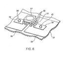
Fig. 8 is a perspective view for explaining one example of the layout and connection of LED bare chips in an LED device. -
Fig. 9 is a perspective view for explaining another example of the layout and connection of LED bare chips in an LED device. -
Fig. 10 is a perspective view for explaining still another example of the layout and connection of LED bare chips in an LED device. -
Fig. 11 is a perspective view of an LED device according to another embodiment of this invention. -
Fig. 12 is a perspective view showing only the main part of the LED device ofFig. 11 by cutting out part of it. -
Fig. 13 shows a modification of the light-emitting apparatus, wherein (a) is a perspective view thereof in a disassembled state, (b) is a perspective view thereof in an assembled state, and (c) is a side view thereof in the assembled state. -
Fig. 14 shows another modification of the light-emitting apparatus, wherein (a) is a perspective view thereof under assembly from its back surface side, (b) is a perspective view thereof under assembly from its front surface side, (c) is a perspective view thereof in an assembled state from its front surface side, and (d) is a side view thereof in the assembled state. -
Fig. 15 is a perspective view showing still another modification of the light-emitting apparatus. -
Fig. 16 is a perspective view for explaining one example of a connection method that can be used for the light-emitting apparatus ofFig. 15 . -
Fig. 17 is a perspective view for explaining another example of a connection method that can be used for the light-emitting apparatus ofFig. 15 . -
Fig. 18 is a perspective view for explaining still another example of a connection method that can be used for the light-emitting apparatus ofFig. 15 . -
Fig. 19 is a perspective view showing still another modification of the light-emitting apparatus. -
Fig. 20 is a perspective view showing still another modification of the light-emitting apparatus. -
Fig. 21 shows still another modification of the light-emitting apparatus, wherein (a) is a perspective view thereof in a disassembled state and (b) is a perspective view thereof in an assembled state. -
Fig. 22 is a perspective view of still another modification of the light-emitting apparatus in a disassembled state. -
Fig. 23 shows still another modification of the light-emitting apparatus, wherein (a) is a perspective view thereof under assembly, (b) is a perspective view thereof in a state where the assembly has been further advanced, and (c) is a perspective view thereof in an assembly completed state. -
Fig. 24 is a cross-sectional view for explaining an LED illumination system disclosed in Patent Document 1 (JP-A-2004-199896 - Referring first to
Fig. 1 , a description will be given of a method of manufacturing LED devices according to an embodiment of this invention. - In the manufacture of the LED devices, a
metal lead frame 21 having a shape shown inFig. 1 (a) is prepared. Thelead frame 21 is integrally formed with a number ofmetal pieces 22 of a predetermined shape which will be metal contacts in a later process. Themetal pieces 22 respectively form pairs which are arranged in a matrix on thelead frame 21. - Proceeding to
Fig. 1 (b) , engineering plastic is molded or insert-molded for each pair of themetal pieces 22, thereby forming adevice body 23 of a predetermined shape which partially covers themetal pieces 22. In this event, arecess 24 is formed in an upper surface of thedevice body 23 so that end portions of the pairedmetal pieces 22 are exposed at positions adjacent to each other at the bottom of therecess 24. - Proceeding to
Fig. 1 (c) , two LED bare chips (light-emitting elements) 25 are fixedly mounted in therecess 24 of eachdevice body 23 by Au-Sn eutectic soldering or the like. In this event, the singlebare chip 25 is placed in contact with the end portion of eachmetal piece 22 and, further, later-described conductive wires are electrically connected between themetal pieces 22 and thebare chips 25 and between thebare chips 25, respectively. In this manner, a number ofLED devices 27 are formed on thelead frame 21. - Thereafter, portions, coupled to the
lead frame 21, of themetal pieces 22 are cut, thereby separating theLED devices 27 from thelead frame 21. In this manner, theLED devices 27, one of which is shown inFig. 1 (d) , can be relatively easily manufactured in large number. Finally, resin is filled into therecesses 24 of thedevice bodies 23 and cured. - Herein, referring particularly to
Fig. 1 (d) , the manufacturedLED device 27 will be described. - The
LED device 27 includes a pair ofmetal contacts 28 formed by themetal pieces 22 shown inFig. 1 (a) . While themetal contacts 28 are insert-molded to thedevice body 23, eachmetal contact 28 has one end exposed in therecess 24 of thedevice body 23 and the other end protruding downward from a lower surface of thedevice body 23 so as to form a plate-shapedterminal portion 29. - In the
LED device 27, thebare chips 25 are placed in direct contact with themetal contacts 28, respectively. Accordingly, it is configured that power supply to thebare chips 25 and heat conduction from thebare chips 25 are carried out through themetal contacts 28. Further, since theLED device 27 has the pair ofmetal contacts 28 and thebare chip 25 is mounted, in equal number, on each of the pairedmetal contacts 28, the heat conduction from thebare chips 25 are uniformly dispersed to the pairedmetal contacts 28 and therefore excellent heat dissipation can be expected. - As described above, since the
metal contacts 28 are each used to conduct both heat and electricity, it is possible to provide the LED device which is simple in structure and inexpensive. - Referring next to
Figs. 2 to 4 , a description will be given of a light-emitting apparatus using theLED device 27 shown inFig. 1 (d) . - This light-emitting apparatus comprises the
LED device 27 and asocket connector 31 which is capable of fitting and releasing theLED device 27. Thesocket connector 31 comprises an insulatinghousing 32 made of plastic or the like and a number of metal springs 33 made of a material with a high thermal conductivity and attached to thehousing 32. Thehousing 32 has two elongatedholes 34 that respectively receive therein the twoterminal portions 29 of theLED device 27. - The metal springs 33 are provided in plurality, for example, in the number of five, corresponding to each
elongated hole 34 of thehousing 32 and are arranged at intervals in the longitudinal direction of eachelongated hole 34. Eachmetal spring 33 has acontact portion 35 disposed in theelongated hole 34 and a connectingportion 36 led out from thecontact portion 35 to the outside of thehousing 32. The connectingportions 36 are divided so as to correspond to one or the other of the twoelongated holes 34 and are respectively connected to twointerconnections 38, which are formed on an attachingobject 37 such as a board, using a technique such as reflow soldering. In this manner, thesocket connector 31 can be surface-mounted on the attachingobject 37. - When the
LED device 27 is fitted to thesocket connector 31, theterminal portions 29 of themetal contacts 28 are inserted into theelongated holes 34 so as to be brought into contact with the plurality ofcontact portions 35 in a lump which are disposed therein. As a result, heats separately transmitted to the twometal contacts 28 from the twobare chips 25 are respectively dispersed to the plurality of metal springs 33 and further transmitted to the attachingobject 37 through the connectingportions 36. Accordingly, excellent heat dissipation can be expected. Simultaneously, there are formed electrical paths each of which reaches thebare chip 25 from theinterconnection 38 of the attachingobject 37 through the metal springs 33 and themetal contact 28. Accordingly, it is possible to supply power to eachbare chip 25 through the metal springs 33 and themetal contact 28. - According to this light-emitting apparatus, since the
socket connector 31 can be mounted on the attachingobject 37 in the state where theLED device 27 is not fitted, it is possible to prevent heat damage to theLED device 27 due to the reflow soldering and to prevent connection failure of theLED device 27 due to the occurrence of solder cracks after the mounting. Further, since thesocket connector 31 which is capable of fitting and releasing theLED device 27 is used, it is possible to easily replace theLED device 27. Further, since contraction due to the difference in linear expansion coefficient between theLED device 27 and the solder is relaxed by spring contacts of the metal springs 33, a highly reliable connection function is achieved. - While the description has been given above of the example in which the
socket connector 31 is mounted on the attachingobject 37 by connecting the plurality of connectingportions 36 to theinterconnections 38, thesocket connector 31 can also be mounted on the attachingobject 37 by each of the structures shown inFigs. 5 to 7 . - In
Fig. 5 , connecting portions respectively provided to a plurality of metal springs 33 of asocket connector 31 are integrally formed together in advance, thereby obtaining a single connection plate 36'. Then, the connection plates 36' are fixed to an attachingobject 37 by tighteningscrews 41, thereby electrically connecting the connection plates 36' to interconnections 38 on the attachingobject 37. - In
Fig. 6 , connecting portions respectively provided to a plurality of metal springs 33 of asocket connector 31 are integrally formed together in advance, thereby obtaining a single connection plate 36'. Consequently, thesocket connector 31 is formed without using the above-mentionedhousing 32. Then, the connection plates 36' are fixed to an attachingobject 37 usingsocket welding 42, thereby electrically connecting the connection plates 36' to interconnections 38 on the attachingobject 37. - It is of course possible to use the above-mentioned
housing 32 also in thesocket connector 31 shown inFig. 6 . An example using thehousing 32 is shown inFigs. 6A to 6C . - Also in
Fig. 7 , connecting portions respectively provided to a plurality of metal springs 33 of asocket connector 31 are integrally formed together in advance, thereby obtaining a single connection plate 36'. Consequently, thesocket connector 31 is formed without using the above-mentionedhousing 32. Then, the connection plates 36' are fixed to an attachingobject 37 usingsocket caulking 43, thereby electrically connecting the connection plates 36' to interconnections 38 on the attachingobject 37. - While the description has been given above of the example in which the connection plates 36' are connected to the
interconnections 38 on the attachingobject 37, the connection plates 36' may alternatively be joined to electrically independent metal plates. - It is of course possible to use the above-mentioned
housing 32 also in thesocket connector 31 shown inFig. 7 . - Referring next to
Figs. 8 to 10 , a description will be given of some examples of the layout and connection ofbare chips 25 in anLED device 27. - In an
LED device 27 ofFig. 8 , twobare chips 25 are respectively mounted with respect to twometal contacts 28. The twobare chips 25 are electrically connected to each other by aconductive wire 44. Further, the twobare chips 25 are each electrically connected to the correspondingmetal contact 28 by aconductive wire 45. - In an
LED device 27 ofFig. 9 , fourbare chips 25 are mounted with respect to twometal contacts 28 such that the twobare chips 25 are mounted on eachmetal contact 28. The twobare chips 25 mounted on one of themetal contacts 28 and the twobare chips 25 mounted on the other of themetal contacts 28 are electrically connected to each other byconductive wires 46. Further, the fourbare chips 25 are each electrically connected to the correspondingmetal contact 28 by aconductive wire 47. - In an
LED device 27 ofFig. 10 , sixbare chips 25 are mounted with respect to twometal contacts 28 such that the threebare chips 25 are mounted on eachmetal contact 28. The sixbare chips 25 are each electrically connected to the twometal contacts 28 byconductive wires - In
Fig. 8 , the two LED bare chips are connected in series while, inFig. 9 , the two LED bare chips are connected in series so that two series structures are arranged side by side. InFig. 10 , the six LED bare chips are connected in parallel. In this manner, the wiring configuration may be suitably determined. While the description has been given of the case where theLED device 27 has two plus and minus terminals (has two terminal portions 29), the same number of bare chips may be mounted on each contact likewise even in the case of four terminals or six terminals. The reason is that, by distributing the generated heat from thebare chips 25 in theLED device 27 equally by the number ofterminal portions 29, the heat can be uniformly transmitted from theterminal portions 29 to the attachingobject 37 such as a mounting board or a housing. That is, by providing the same number ofbare chips 25 on each of the pairedmetal contacts 28, the generated heat from thebare chips 25 can be equally distributed to theterminal portions 29. In this manner, by equally distributing the generated heat from thebare chips 25 to theterminal portions 29, it is possible to prevent the localization of heat and thus to reduce the difference in stress to be generated so that the reliability is improved. Assuming that the number ofterminal portions 29 of theLED device 27 is n (n≥2), the number ofbare chips 25 that are mounted in theLED device 27 becomes a multiple of n. -
Figs. 11 and 12 show an LED device 27' according to another embodiment of this invention. This LED device 27' has fourterminal portions 29. Out of the fourterminal portions 29, the two are minus terminals and the other two are plus terminals. That is, the single LED device 27' has the two plus terminals and the two minus terminals. In this manner, by providing the plurality of plus terminals and the plurality of minus terminals, it is possible to individually control LEDs that emit different colors of light, which is convenient for adjusting the color. -
Fig. 13 shows a modification of the light-emitting apparatus. The same reference symbols are assigned to those portions having the same functions, thereby omitting an explanation thereof. - In a
socket connector 31 used in the light-emitting apparatus ofFig. 13 , portions of metal springs 33 are held by ahousing 32. As shown in (a), thesocket connector 31 is mounted on a surface of an attachingobject 37 such as a board using a mounter and the other portions of the metal springs 33 are respectively connected to twointerconnections 38, which are disposed to be spaced apart from each other, of the attachingobject 37 using a technique such as reflow soldering. - Then, as shown in (b) and (c), an
LED device 27 is fitted to thesocket connector 31. The relationship between theLED device 27 and thesocket connector 31 may be the same as one of the various examples described above. -
Fig. 14 shows another modification of the light-emitting apparatus. The same reference symbols are assigned to those portions having the same functions, thereby omitting an explanation thereof. - Also in a
socket connector 31 used in the light-emitting apparatus ofFig. 14 , portions of metal springs 33 are held by ahousing 32. A throughhole 51 is formed in an attachingobject 37 from its front to back. Using this throughhole 51, thesocket connector 31 is mounted on the attachingobject 37. That is, as shown in (a), thesocket connector 31 is inserted down into the throughhole 51 in a posture which is upside down as compared with that inFig. 13 (a) , and the other portions of the metal springs 33 are respectively connected to twointerconnections 38, which are disposed to be spaced apart from each other, of the attachingobject 37 using a technique such as reflow soldering. - After mounting the
socket connector 31 on the attachingobject 37 as described above, the attachingobject 37 is turned over as shown in (b) and then anLED device 27 is fitted to thesocket connector 31 as shown in (c) and (d). The relationship between theLED device 27 and thesocket connector 31 may be the same as one of the various examples described above. - According to the light-emitting apparatus of
Fig. 14 , it is possible to reduce the dimension in a thickness direction of the attachingobject 37. -
Fig. 15 shows still another modification of the light-emitting apparatus. The same reference symbols are assigned to those portions having the same functions, thereby omitting an explanation thereof. - The light-emitting apparatus of
Fig. 15 uses two electricallyindependent metal plates 52 as attaching objects and interconnections. Between thesemetal plates 52, a plurality ofsocket connectors 31 each having anLED device 27 connected thereto are mounted in a bridging state. Further, metal springs 33 of eachsocket connector 31 are connected to themetal plates 52 by a suitable connection method. One example of the suitable connection method is so-called bus bar mounting. - As another example of the suitable connection method,
laser welding portions 53 shown inFig. 16 , screwingportions 54 shown inFig. 17 , andcaulking portions 55 shown inFig. 18 can be used alone or in combination thereof. -
Fig. 19 shows still another modification of the light-emitting apparatus. The same reference symbols are assigned to those portions having the same functions, thereby omitting an explanation thereof. - The light-emitting apparatus of
Fig. 19 uses, as attaching objects and interconnections, a plurality of, for example, seven, flat plate-shapedmetal plates 56 which are formed by press working or the like and are electrically independent of each other. Thesemetal plates 56 are disposed side by side in a circumferential direction to form a ring shape, a plurality of, for example, six,socket connectors 31 each having anLED device 27 connected thereto are mounted in a bridging state between theadjacent metal plates 56, and metal springs 33 are connected to themetal plates 56, thereby forming a series circuit. In this case, the twometal plates 56, located at both ends of the series circuit, of the sevenmetal plates 56 are each provided with a connectingportion 57 by bending andharness terminals 58 are fitted and connected to the connectingportions 57 so that themetal plates 56 can be fixed to the harness. The plurality of metal plates are arranged in the circumferential direction. - Each metal plate 56 (52) is not limited to the flat plate shape, but may be, for example, an angled member as shown in
Fig. 20 . -
Fig. 21 shows still another modification of the light-emitting apparatus. The same reference symbols are assigned to those portions having the same functions, thereby omitting an explanation thereof. - The light-emitting apparatus of
Fig. 21 comprises a disc-shapedhousing 61 made of an insulator, a first ring-shapedmetal plate 62 disposed on a disc-shaped surface of thehousing 61, a secondpolygonal metal plate 63 disposed on the disc-shaped surface of thehousing 61 inward of thefirst metal plate 62, and a disc-shaped insulatingreflector 64, as a separate component, having an outer diameter equal to that of thefirst metal plate 62. The first andsecond metal plates second metal plates - As shown in (a), an inner peripheral face of the
first metal plate 62 faces an outer peripheral face of thesecond metal plate 63 with a substantially uniform gap therebetween on the disc-shaped surface of thehousing 61 and therefore the first andsecond metal plates socket connectors 31 each having anLED device 27 connected thereto are placed in a bridging state between the first andsecond metal plates socket connector 31 are in contact with the first andsecond metal plates - In (a), further, the
reflector 64 is overlaid on the first andsecond metal plates socket connectors 31 are respectively inserted into a plurality ofholes 65 formed in thereflector 64. Further, thereflector 64 is tightly fixed to thehousing 61 usingscrew rods 66 or the like. Consequently, by thereflector 64, the metal springs 33 of thesocket connectors 31 are pressed to the first andsecond metal plates socket connectors 31 are fixed. - In this manner, the light-emitting apparatus shown in (b) is obtained.
- In
Fig. 21 , the sixLED devices 27 and the sixsocket connectors 31 are used. However, the number of them may be suitably changed as inFig. 22 which shows a case of three. -
Fig. 23 shows still another modification of the light-emitting apparatus. The same reference symbols are assigned to those portions having the same functions, thereby omitting an explanation thereof. - The light-emitting apparatus of
Fig. 23 comprises a rectangular plate-shapedhousing 71 made of an insulator, twometal plates 72 adjacently disposed on a rectangular surface of thehousing 71, and an insulatingreflection sheet 73 covering themetal plates 72. Themetal plates 72 can be formed by press working or the like and respectively have a plurality of semicircular recesses on their mutually facing sides. These semicircular recesses cooperatively form a plurality of substantiallycircular holes 74 when the twometal plates 72 are disposed adjacent to each other. Thereflection sheet 73 has a plurality ofsmall holes 75 which are in one-to-one correspondence with theholes 74. - As shown in (a), a plurality of
socket connectors 31 each having anLED device 27 connected thereto are disposed so as to be spaced apart from each other on the rectangular surface of thehousing 71. Then, the twometal plates 72 are adjacently disposed with a gap therebetween on the rectangular surface of thehousing 71. Therefore, the twometal plates 72 are electrically independent of each other and are used as attaching objects and interconnections. Further, themetal plates 72 are tightly fixed to thehousing 71 usingscrew rods 76 or the like. Consequently, themetal plates 72 are pressed to metal springs 33 of thesocket connectors 31 so as to be electrically connected thereto and so as to fix the positions of thesocket connectors 31. - Further, as shown in (b), the
reflection sheet 73 is disposed on themetal plates 72. In this event, theLED devices 27 are respectively inserted into thesmall holes 75 of thereflection sheets 73. In this manner, the light-emitting apparatus shown in (c) is obtained. According to this light-emitting apparatus, since thereflection sheet 73 is used, it is possible to effectively use the light of theLED devices 27. - Part or the whole of the above-mentioned embodiments can also be described as the following supplementary notes but is not limited thereto.
- An LED device characterized in that an LED
bare chip 25 is mounted directly on ametal contact 28 and power supply to thebare chip 25 and heat conduction from thebare chip 25 are carried out through themetal contact 28. - The LED device according to
supplementary note 1, characterized by comprising a pair ofmetal contacts 28, wherein thebare chip 25 is provided, in equal number, on each of the pair ofmetal contacts 28. - The LED device according to
supplementary note device body 23 made of plastic and insert-molded with themetal contact 28, wherein the metal contact 28has aterminal portion 29 protruding outward from thedevice body 23. - A method of manufacturing the LED device according to any one of
supplementary notes 1 to 3, characterized by preparing alead frame 21 formed with the pair ofmetal contacts 28, forming a device body by insert-molding the pair ofmetal contacts 28 with the plastic, mounting thebare chips 25 on the pair ofmetal contacts 28 to form the LED device on thelead frame 21, and then cutting themetal contacts 28 to separate the LED device from thelead frame 21. - A light-emitting apparatus characterized by comprising the LED device according to any one of
supplementary notes 1 to 3 and aconnector 31 adapted to be attached to an attachingobject 37 and capable of fitting themetal contacts 28, wherein power is supplied to thebare chips 25 from the attachingobject 37 through theconnector 31 and themetal contacts 28 and heat of the bare chips is transmitted to the attachingobject 37 through themetal contacts 28 and theconnector 31 to carry out heat dissipation. - The light-emitting apparatus according to
supplementary note 5, characterized by further comprising the attachingobject 37, wherein a plurality ofinterconnections 38 are formed on a surface of the attachingobject 37, theconnector 31 is disposed in a bridging state between theinterconnections 38, and themetal contacts 28 are connected to theinterconnections 38. - The light-emitting apparatus according to
supplementary note 5, characterized by further comprising, as the attachingobject 37, a plurality of metal plates which are disposed adjacent to each other and are electrically independent of each other, wherein theconnector 31 is disposed in a bridging state between the adjacent metal plates and themetal contacts 28 are connected to the metal plates. - The light-emitting apparatus according to
supplementary note 7, characterized in that the plurality of metal plates are arranged parallel to each other. - The light-emitting apparatus according to
supplementary note 7, characterized in that the plurality of metal plates are arranged in a circumferential direction. - The light-emitting apparatus according to
supplementary note 7, characterized in that the plurality of metal plates are arranged in a radial direction. - The light-emitting apparatus according to any one of
supplementary notes 6 to 10, characterized by further comprising a separate component that fixes theconnector 31 to the attachingobject 37. - The light-emitting apparatus according to supplementary note 11, characterized in that the separate component is insulating.
- While this invention has been described with reference to the embodiments, this invention is not limited thereto. Various changes that can be understood by those skilled in the art can be made to the structures and details of this invention within the scope of this invention.
- This application claims the benefit of priority from Japanese Patent Application No.
2010-18719, filed on January 29, 2010 - This invention is applicable to general illumination, streetlights, car backlights, and so on.
-
- 1
- substrate
- 2
- heat transfer layer
- 3
- conductive layer
- 4
- LED chip
- 5, 6
- terminals of conductive layer
- 7, 8
- electrodes of LED chip
- 9
- heat contact portion of conductive layer
- 21
- lead frame
- 22
- metal piece
- 23
- device body
- 24
- recess
- 25
- LED bare chip (light-emitting element)
- 27
- LED device
- 27'
- LED device
- 28
- metal contact
- 29
- terminal portion
- 31
- socket connector (connector)
- 32
- housing
- 33
- metal spring
- 34
- elongated hole
- 35
- contact portion
- 36
- connecting portion
- 36'
- connection plate
- 37
- attaching object
- 38
- interconnection
- 41
- screw
- 42
- socket welding
- 43
- socket caulking
- 44 to 49
- conductive wires
- 51
- through hole
- 52
- metal plate
- 53
- laser welding portion
- 54
- screwing portion
- 55
- caulking portion
- 56
- metal plate
- 57
- connecting portion
- 58
- harness terminal
- 61
- housing
- 62
- first metal plate
- 63
- second metal plate
- 64
- reflector
- 65
- hole
- 66
- screw rod
- 71
- housing
- 72
- metal plate
- 73
- reflection sheet
- 74
- hole
Claims (2)
- An LED device (27, 27') characterized by comprising:a pair of metal contacts (28);a device body (23) made of plastic by insert-molding the metal contacts (28) to have a recess (24) on an upper surface thereof, one ends of the pair of metal contacts (28) being exposed adjacent to each other at a bottom of the recess (24) of the device body (23), the other ends of the pair of metal contacts (28) protruding from a lower surface of the device body (23); andan LED bare chip (25) placed in the recess (24) of the device body (23) and mounted directly on the one ends of the pair of metal contacts (28), wherein power supply to the bare chip (25) and heat conduction from the bare chip (25) are carried out through the metal contacts (28).
- An LED device (27, 27') as claimed in claim 1, characterized by further comprising an additional metal contact (28), the metal contacts (28) making a pair, wherein the bare chip (25) is provided, in equal number, on each of the pair of metal contacts (28).
Priority Applications (1)
| Application Number | Priority Date | Filing Date | Title |
|---|---|---|---|
| EP17200933.4A EP3309848B1 (en) | 2010-01-29 | 2011-01-18 | Led device, method of manufacturing the same, and light-emitting apparatus |
Applications Claiming Priority (2)
| Application Number | Priority Date | Filing Date | Title |
|---|---|---|---|
| JP2010018719 | 2010-01-29 | ||
| EP11736889.4A EP2515354B1 (en) | 2010-01-29 | 2011-01-18 | Method for manufacturing an led device |
Related Parent Applications (2)
| Application Number | Title | Priority Date | Filing Date |
|---|---|---|---|
| EP11736889.4A Division EP2515354B1 (en) | 2010-01-29 | 2011-01-18 | Method for manufacturing an led device |
| EP11736889.4A Division-Into EP2515354B1 (en) | 2010-01-29 | 2011-01-18 | Method for manufacturing an led device |
Related Child Applications (2)
| Application Number | Title | Priority Date | Filing Date |
|---|---|---|---|
| EP17200933.4A Division-Into EP3309848B1 (en) | 2010-01-29 | 2011-01-18 | Led device, method of manufacturing the same, and light-emitting apparatus |
| EP17200933.4A Division EP3309848B1 (en) | 2010-01-29 | 2011-01-18 | Led device, method of manufacturing the same, and light-emitting apparatus |
Publications (2)
| Publication Number | Publication Date |
|---|---|
| EP2854187A1 true EP2854187A1 (en) | 2015-04-01 |
| EP2854187B1 EP2854187B1 (en) | 2018-03-07 |
Family
ID=44319166
Family Applications (5)
| Application Number | Title | Priority Date | Filing Date |
|---|---|---|---|
| EP11736889.4A Not-in-force EP2515354B1 (en) | 2010-01-29 | 2011-01-18 | Method for manufacturing an led device |
| EP17160854.0A Not-in-force EP3214662B1 (en) | 2010-01-29 | 2011-01-18 | Light-emitting apparatus |
| EP17200933.4A Active EP3309848B1 (en) | 2010-01-29 | 2011-01-18 | Led device, method of manufacturing the same, and light-emitting apparatus |
| EP14180793.3A Not-in-force EP2854187B1 (en) | 2010-01-29 | 2011-01-18 | LED device, method of manufacturing the same, and light-emitting apparatus |
| EP14180822.0A Not-in-force EP2854188B1 (en) | 2010-01-29 | 2011-01-18 | LED device, method of manufacturing the same, and light-emitting apparatus |
Family Applications Before (3)
| Application Number | Title | Priority Date | Filing Date |
|---|---|---|---|
| EP11736889.4A Not-in-force EP2515354B1 (en) | 2010-01-29 | 2011-01-18 | Method for manufacturing an led device |
| EP17160854.0A Not-in-force EP3214662B1 (en) | 2010-01-29 | 2011-01-18 | Light-emitting apparatus |
| EP17200933.4A Active EP3309848B1 (en) | 2010-01-29 | 2011-01-18 | Led device, method of manufacturing the same, and light-emitting apparatus |
Family Applications After (1)
| Application Number | Title | Priority Date | Filing Date |
|---|---|---|---|
| EP14180822.0A Not-in-force EP2854188B1 (en) | 2010-01-29 | 2011-01-18 | LED device, method of manufacturing the same, and light-emitting apparatus |
Country Status (7)
| Country | Link |
|---|---|
| US (1) | US9425372B2 (en) |
| EP (5) | EP2515354B1 (en) |
| JP (1) | JP5871621B2 (en) |
| KR (1) | KR101398701B1 (en) |
| CN (2) | CN107275467B (en) |
| TW (1) | TWI467816B (en) |
| WO (1) | WO2011093174A1 (en) |
Families Citing this family (28)
| Publication number | Priority date | Publication date | Assignee | Title |
|---|---|---|---|---|
| JP5528900B2 (en) * | 2010-04-30 | 2014-06-25 | ローム株式会社 | Light emitting element module |
| DE102011056708A1 (en) | 2011-12-20 | 2013-06-20 | Osram Opto Semiconductors Gmbh | Process for the production of optoelectronic semiconductor components, lead frame composite and optoelectronic semiconductor component |
| DE102011056700A1 (en) | 2011-12-20 | 2013-06-20 | Osram Opto Semiconductors Gmbh | Process for the production of optoelectronic semiconductor components, lead frame composite and optoelectronic semiconductor component |
| KR101276576B1 (en) | 2012-02-16 | 2013-06-18 | 오름반도체 주식회사 | Module for lighting emitting diode |
| JP5956815B2 (en) * | 2012-04-20 | 2016-07-27 | 日本航空電子工業株式会社 | Optical module substrate and optical module |
| DE102012104882B4 (en) * | 2012-06-05 | 2017-06-08 | Osram Opto Semiconductors Gmbh | Process for the production of optoelectronic semiconductor components and thus produced optoelectronic semiconductor component |
| US10591124B2 (en) | 2012-08-30 | 2020-03-17 | Sabic Global Technologies B.V. | Heat dissipating system for a light, headlamp assembly comprising the same, and method of dissipating heat |
| US9565782B2 (en) * | 2013-02-15 | 2017-02-07 | Ecosense Lighting Inc. | Field replaceable power supply cartridge |
| WO2015139995A1 (en) * | 2014-03-21 | 2015-09-24 | Koninklijke Philips N.V. | Lighting device with an improved housing |
| DE102014220188B3 (en) * | 2014-10-06 | 2016-02-11 | E.G.O. Elektro-Gerätebau GmbH | display device |
| US10477636B1 (en) | 2014-10-28 | 2019-11-12 | Ecosense Lighting Inc. | Lighting systems having multiple light sources |
| US11306897B2 (en) | 2015-02-09 | 2022-04-19 | Ecosense Lighting Inc. | Lighting systems generating partially-collimated light emissions |
| US9869450B2 (en) | 2015-02-09 | 2018-01-16 | Ecosense Lighting Inc. | Lighting systems having a truncated parabolic- or hyperbolic-conical light reflector, or a total internal reflection lens; and having another light reflector |
| US9651216B2 (en) | 2015-03-03 | 2017-05-16 | Ecosense Lighting Inc. | Lighting systems including asymmetric lens modules for selectable light distribution |
| US9568665B2 (en) | 2015-03-03 | 2017-02-14 | Ecosense Lighting Inc. | Lighting systems including lens modules for selectable light distribution |
| US9746159B1 (en) | 2015-03-03 | 2017-08-29 | Ecosense Lighting Inc. | Lighting system having a sealing system |
| US9651227B2 (en) | 2015-03-03 | 2017-05-16 | Ecosense Lighting Inc. | Low-profile lighting system having pivotable lighting enclosure |
| USD785218S1 (en) | 2015-07-06 | 2017-04-25 | Ecosense Lighting Inc. | LED luminaire having a mounting system |
| USD782093S1 (en) | 2015-07-20 | 2017-03-21 | Ecosense Lighting Inc. | LED luminaire having a mounting system |
| USD782094S1 (en) | 2015-07-20 | 2017-03-21 | Ecosense Lighting Inc. | LED luminaire having a mounting system |
| US9651232B1 (en) | 2015-08-03 | 2017-05-16 | Ecosense Lighting Inc. | Lighting system having a mounting device |
| TWI622187B (en) * | 2015-11-23 | 2018-04-21 | Unity Opto Technology Co Ltd | LED light emitting device manufacturing method and LED light emitting device |
| CN108475712B (en) * | 2015-12-01 | 2021-11-09 | 夏普株式会社 | Image forming element |
| DE102016103123A1 (en) * | 2016-02-23 | 2017-08-24 | Vishay Semiconductor Gmbh | Optoelectronic device |
| DE102016103144A1 (en) | 2016-02-23 | 2017-08-24 | Vishay Semiconductor Gmbh | Optoelectronic device |
| DE102016103113A1 (en) | 2016-02-23 | 2017-08-24 | Vishay Semiconductor Gmbh | Optoelectronic device |
| DE102016103136A1 (en) | 2016-02-23 | 2017-08-24 | Vishay Semiconductor Gmbh | Optoelectronic device |
| CN109782856B (en) * | 2019-03-20 | 2024-01-26 | 南京工程学院 | Active disassembly structure of tablet personal computer |
Citations (10)
| Publication number | Priority date | Publication date | Assignee | Title |
|---|---|---|---|---|
| US5404282A (en) * | 1993-09-17 | 1995-04-04 | Hewlett-Packard Company | Multiple light emitting diode module |
| US20030151343A1 (en) * | 2000-06-15 | 2003-08-14 | Balu Jeganathan | Method of producing a lamp |
| JP2003303936A (en) * | 2002-04-12 | 2003-10-24 | Matsushita Electric Ind Co Ltd | Lead frame and manufacturing method thereof, and chip type led employing the lead frame |
| US20030218417A1 (en) * | 2002-05-22 | 2003-11-27 | Unity Opto Technology Co., Ltd. | Light emitting diode lamp with light emitting diode module having improved heat dissipation |
| JP2004199896A (en) | 2002-12-16 | 2004-07-15 | Junichi Shimada | Led illumination system |
| US20050199900A1 (en) * | 2004-03-12 | 2005-09-15 | Ming-Der Lin | Light-emitting device with high heat-dissipating efficiency |
| US20080042151A1 (en) * | 2006-07-10 | 2008-02-21 | Samsung Electro-Mechanics Co., Ltd. | High power light emitting diode package and method of producing the same |
| DE202007012162U1 (en) * | 2007-06-05 | 2008-03-20 | Seoul Semiconductor Co., Ltd. | LED housing |
| US20090001393A1 (en) * | 2007-06-29 | 2009-01-01 | Seoul Semiconductor Co., Ltd. | Multi-light emitting diode package |
| US20090283781A1 (en) * | 2008-05-16 | 2009-11-19 | Cree Hong Kong Limited | Mini V SMD |
Family Cites Families (30)
| Publication number | Priority date | Publication date | Assignee | Title |
|---|---|---|---|---|
| JPS61171089U (en) | 1985-04-10 | 1986-10-23 | ||
| JPH08116096A (en) | 1994-10-14 | 1996-05-07 | Hamamatsu Photonics Kk | Light emitting device |
| US6274924B1 (en) * | 1998-11-05 | 2001-08-14 | Lumileds Lighting, U.S. Llc | Surface mountable LED package |
| US6386733B1 (en) * | 1998-11-17 | 2002-05-14 | Ichikoh Industries, Ltd. | Light emitting diode mounting structure |
| US6521916B2 (en) | 1999-03-15 | 2003-02-18 | Gentex Corporation | Radiation emitter device having an encapsulant with different zones of thermal conductivity |
| AUPQ818100A0 (en) * | 2000-06-15 | 2000-07-06 | Arlec Australia Limited | Led lamp |
| AUPR570501A0 (en) | 2001-06-15 | 2001-07-12 | Q1 (Pacific) Limited | Led lamp |
| US6541800B2 (en) * | 2001-02-22 | 2003-04-01 | Weldon Technologies, Inc. | High power LED |
| JP4095463B2 (en) * | 2003-02-13 | 2008-06-04 | 松下電器産業株式会社 | LED light source socket |
| DE102004063978B4 (en) * | 2003-07-17 | 2019-01-24 | Toyoda Gosei Co., Ltd. | Light-emitting device |
| JP2005159296A (en) * | 2003-11-06 | 2005-06-16 | Sharp Corp | Package structure of optodevice |
| JP2005317661A (en) * | 2004-04-27 | 2005-11-10 | Sharp Corp | Semiconductor light emitting device and its manufacturing method |
| KR100558454B1 (en) * | 2004-06-17 | 2006-03-10 | 삼성전기주식회사 | Detachable light emitting diode for vehicle and module thereof |
| KR100587020B1 (en) * | 2004-09-01 | 2006-06-08 | 삼성전기주식회사 | High power light emitting diode package |
| WO2006059828A1 (en) * | 2004-09-10 | 2006-06-08 | Seoul Semiconductor Co., Ltd. | Light emitting diode package having multiple molding resins |
| US7677763B2 (en) * | 2004-10-20 | 2010-03-16 | Timothy Chan | Method and system for attachment of light emitting diodes to circuitry for use in lighting |
| JP2006165101A (en) | 2004-12-03 | 2006-06-22 | Harison Toshiba Lighting Corp | Envelope for light-emitting device |
| JP2006165097A (en) * | 2004-12-03 | 2006-06-22 | Harison Toshiba Lighting Corp | Envelope for light-emitting element |
| KR100616684B1 (en) | 2005-06-03 | 2006-08-28 | 삼성전기주식회사 | High power led package and fabrication method thereof |
| JP4582786B2 (en) | 2005-06-16 | 2010-11-17 | ニチコン株式会社 | Light source device |
| JP2007080878A (en) | 2005-09-09 | 2007-03-29 | Matsushita Electric Works Ltd | Light emitting device |
| DE112006004259A5 (en) * | 2005-11-21 | 2012-09-06 | Seoul Semiconductor Co., Ltd. | Light-emitting element |
| JP4430737B2 (en) * | 2006-10-18 | 2010-03-10 | 伸壹 坪田 | LED unit manufacturing method |
| TW200843135A (en) | 2007-04-23 | 2008-11-01 | Augux Co Ltd | Method of packaging light emitting diode with high heat-dissipating efficiency and the structure thereof |
| JP2008300553A (en) * | 2007-05-30 | 2008-12-11 | I-Chiun Precision Industry Co Ltd | Manufacturing method of frame combination member for surface mounted light emitting diode, and structure thereof |
| US7923831B2 (en) | 2007-05-31 | 2011-04-12 | Avago Technologies Ecbu Ip (Singapore) Pte. Ltd. | LED-based light source having improved thermal dissipation |
| KR100801621B1 (en) | 2007-06-05 | 2008-02-11 | 서울반도체 주식회사 | Led package |
| CN101533819B (en) * | 2008-03-14 | 2013-01-16 | 旭丽电子(广州)有限公司 | Semiconductor packaging structure, lead frame and conductive part which are applied to semiconductor packaging structure |
| JP2009267292A (en) | 2008-04-30 | 2009-11-12 | Toshiba Lighting & Technology Corp | Light-emitting device and luminaire |
| JP2010018719A (en) | 2008-07-11 | 2010-01-28 | Adeka Corp | Silicon-containing curable composition |
-
2011
- 2011-01-18 US US13/521,294 patent/US9425372B2/en active Active
- 2011-01-18 EP EP11736889.4A patent/EP2515354B1/en not_active Not-in-force
- 2011-01-18 EP EP17160854.0A patent/EP3214662B1/en not_active Not-in-force
- 2011-01-18 JP JP2011551810A patent/JP5871621B2/en not_active Expired - Fee Related
- 2011-01-18 CN CN201710231007.8A patent/CN107275467B/en not_active Expired - Fee Related
- 2011-01-18 KR KR1020127018028A patent/KR101398701B1/en active IP Right Grant
- 2011-01-18 WO PCT/JP2011/050756 patent/WO2011093174A1/en active Application Filing
- 2011-01-18 EP EP17200933.4A patent/EP3309848B1/en active Active
- 2011-01-18 EP EP14180793.3A patent/EP2854187B1/en not_active Not-in-force
- 2011-01-18 CN CN201180006903.5A patent/CN102754228B/en not_active Expired - Fee Related
- 2011-01-18 EP EP14180822.0A patent/EP2854188B1/en not_active Not-in-force
- 2011-01-28 TW TW100103340A patent/TWI467816B/en not_active IP Right Cessation
Patent Citations (10)
| Publication number | Priority date | Publication date | Assignee | Title |
|---|---|---|---|---|
| US5404282A (en) * | 1993-09-17 | 1995-04-04 | Hewlett-Packard Company | Multiple light emitting diode module |
| US20030151343A1 (en) * | 2000-06-15 | 2003-08-14 | Balu Jeganathan | Method of producing a lamp |
| JP2003303936A (en) * | 2002-04-12 | 2003-10-24 | Matsushita Electric Ind Co Ltd | Lead frame and manufacturing method thereof, and chip type led employing the lead frame |
| US20030218417A1 (en) * | 2002-05-22 | 2003-11-27 | Unity Opto Technology Co., Ltd. | Light emitting diode lamp with light emitting diode module having improved heat dissipation |
| JP2004199896A (en) | 2002-12-16 | 2004-07-15 | Junichi Shimada | Led illumination system |
| US20050199900A1 (en) * | 2004-03-12 | 2005-09-15 | Ming-Der Lin | Light-emitting device with high heat-dissipating efficiency |
| US20080042151A1 (en) * | 2006-07-10 | 2008-02-21 | Samsung Electro-Mechanics Co., Ltd. | High power light emitting diode package and method of producing the same |
| DE202007012162U1 (en) * | 2007-06-05 | 2008-03-20 | Seoul Semiconductor Co., Ltd. | LED housing |
| US20090001393A1 (en) * | 2007-06-29 | 2009-01-01 | Seoul Semiconductor Co., Ltd. | Multi-light emitting diode package |
| US20090283781A1 (en) * | 2008-05-16 | 2009-11-19 | Cree Hong Kong Limited | Mini V SMD |
Also Published As
| Publication number | Publication date |
|---|---|
| US9425372B2 (en) | 2016-08-23 |
| EP2854187B1 (en) | 2018-03-07 |
| CN107275467B (en) | 2019-06-14 |
| KR101398701B1 (en) | 2014-05-27 |
| EP3214662A1 (en) | 2017-09-06 |
| TW201135990A (en) | 2011-10-16 |
| EP3309848A1 (en) | 2018-04-18 |
| KR20120106799A (en) | 2012-09-26 |
| EP2515354A4 (en) | 2013-09-11 |
| CN107275467A (en) | 2017-10-20 |
| EP2854188B1 (en) | 2017-04-26 |
| EP2854188A1 (en) | 2015-04-01 |
| WO2011093174A1 (en) | 2011-08-04 |
| JP5871621B2 (en) | 2016-03-01 |
| JPWO2011093174A1 (en) | 2013-05-30 |
| EP2515354A1 (en) | 2012-10-24 |
| CN102754228A (en) | 2012-10-24 |
| EP3309848B1 (en) | 2022-05-18 |
| US20120292660A1 (en) | 2012-11-22 |
| TWI467816B (en) | 2015-01-01 |
| EP2515354B1 (en) | 2018-03-07 |
| CN102754228B (en) | 2017-10-13 |
| EP3214662B1 (en) | 2018-09-26 |
Similar Documents
| Publication | Publication Date | Title |
|---|---|---|
| EP2515354B1 (en) | Method for manufacturing an led device | |
| US7510400B2 (en) | LED interconnect spring clip assembly | |
| US8933616B2 (en) | Light emitting device with spring-loaded LED-holder | |
| KR101294657B1 (en) | Module for securing LED and Method for manufacturing the same, LED module and Illuminating apparatus using LED module | |
| CN102313170B (en) | Light emitting device and illumination apparatus | |
| CN105720181A (en) | Led lead frame array for general illumination | |
| US20090160302A1 (en) | Led lighting lamp | |
| CN102365491A (en) | Lighting system comprising at least one luminous band | |
| CN102844607A (en) | Array of scalable ceramic diode carriers having leds | |
| TWI594468B (en) | Photoelectric device | |
| CN107453104B (en) | Connector, power supply module and terminal equipment | |
| KR20210110560A (en) | Lighting device comprising a circuit board | |
| CN103196042B (en) | Illuminator and manufacture method thereof | |
| US11430933B2 (en) | Lighting device with high flexibility in connecting electrical components | |
| JP3139079U (en) | LED unit and LED module | |
| KR101138442B1 (en) | Light emitting device |
Legal Events
| Date | Code | Title | Description |
|---|---|---|---|
| PUAI | Public reference made under article 153(3) epc to a published international application that has entered the european phase |
Free format text: ORIGINAL CODE: 0009012 |
|
| 17P | Request for examination filed |
Effective date: 20140813 |
|
| AC | Divisional application: reference to earlier application |
Ref document number: 2515354 Country of ref document: EP Kind code of ref document: P |
|
| AK | Designated contracting states |
Kind code of ref document: A1 Designated state(s): AL AT BE BG CH CY CZ DE DK EE ES FI FR GB GR HR HU IE IS IT LI LT LU LV MC MK MT NL NO PL PT RO RS SE SI SK SM TR |
|
| AX | Request for extension of the european patent |
Extension state: BA ME |
|
| R17P | Request for examination filed (corrected) |
Effective date: 20150911 |
|
| RBV | Designated contracting states (corrected) |
Designated state(s): AL AT BE BG CH CY CZ DE DK EE ES FI FR GB GR HR HU IE IS IT LI LT LU LV MC MK MT NL NO PL PT RO RS SE SI SK SM TR |
|
| 17Q | First examination report despatched |
Effective date: 20151119 |
|
| STAA | Information on the status of an ep patent application or granted ep patent |
Free format text: STATUS: EXAMINATION IS IN PROGRESS |
|
| RIC1 | Information provided on ipc code assigned before grant |
Ipc: H01L 33/48 20100101AFI20161017BHEP Ipc: F21Y 103/33 20160101ALN20161017BHEP Ipc: F21V 7/05 20060101ALI20161017BHEP Ipc: H01L 33/64 20100101ALI20161017BHEP Ipc: F21K 9/90 20160101ALN20161017BHEP Ipc: H05K 3/30 20060101ALN20161017BHEP Ipc: F21Y 105/10 20160101ALN20161017BHEP Ipc: H01L 25/075 20060101ALN20161017BHEP Ipc: F21Y 115/10 20160101ALI20161017BHEP Ipc: H05K 3/32 20060101ALN20161017BHEP Ipc: F21Y 101/00 20160101ALI20161017BHEP Ipc: H05K 1/02 20060101ALI20161017BHEP Ipc: H01L 33/62 20100101ALN20161017BHEP Ipc: F21V 17/12 20060101ALN20161017BHEP |
|
| RIC1 | Information provided on ipc code assigned before grant |
Ipc: F21V 7/05 20060101ALI20170502BHEP Ipc: F21Y 105/10 20160101ALN20170502BHEP Ipc: H05K 3/32 20060101ALN20170502BHEP Ipc: H01L 33/48 20100101AFI20170502BHEP Ipc: H05K 1/02 20060101ALI20170502BHEP Ipc: H05K 3/30 20060101ALN20170502BHEP Ipc: H01L 33/62 20100101ALN20170502BHEP Ipc: H01L 33/64 20100101ALI20170502BHEP Ipc: H01L 25/075 20060101ALN20170502BHEP Ipc: F21Y 101/00 20160101ALI20170502BHEP Ipc: F21Y 115/10 20160101ALI20170502BHEP Ipc: F21K 9/90 20160101ALN20170502BHEP Ipc: F21V 17/12 20060101ALN20170502BHEP Ipc: F21Y 103/33 20160101ALN20170502BHEP |
|
| RIC1 | Information provided on ipc code assigned before grant |
Ipc: H05K 3/32 20060101ALN20170606BHEP Ipc: F21V 7/05 20060101ALI20170606BHEP Ipc: F21Y 103/33 20160101ALN20170606BHEP Ipc: H05K 1/02 20060101ALI20170606BHEP Ipc: H01L 25/075 20060101ALN20170606BHEP Ipc: H05K 3/30 20060101ALN20170606BHEP Ipc: F21Y 101/00 20160101ALI20170606BHEP Ipc: F21Y 115/10 20160101ALI20170606BHEP Ipc: F21V 17/12 20060101ALN20170606BHEP Ipc: F21K 9/90 20160101ALN20170606BHEP Ipc: H01L 33/64 20100101ALI20170606BHEP Ipc: H01L 33/62 20100101ALN20170606BHEP Ipc: F21Y 105/10 20160101ALN20170606BHEP Ipc: H01L 33/48 20100101AFI20170606BHEP |
|
| GRAP | Despatch of communication of intention to grant a patent |
Free format text: ORIGINAL CODE: EPIDOSNIGR1 |
|
| STAA | Information on the status of an ep patent application or granted ep patent |
Free format text: STATUS: GRANT OF PATENT IS INTENDED |
|
| RIC1 | Information provided on ipc code assigned before grant |
Ipc: F21K 9/90 20160101ALN20170609BHEP Ipc: F21Y 103/33 20160101ALN20170609BHEP Ipc: F21Y 105/10 20160101ALN20170609BHEP Ipc: H01L 33/62 20100101ALN20170609BHEP Ipc: H01L 25/075 20060101ALN20170609BHEP Ipc: F21Y 115/10 20160101ALI20170609BHEP Ipc: F21V 7/05 20060101ALI20170609BHEP Ipc: H05K 1/02 20060101ALI20170609BHEP Ipc: H01L 33/48 20100101AFI20170609BHEP Ipc: H05K 3/32 20060101ALN20170609BHEP Ipc: H05K 3/30 20060101ALN20170609BHEP Ipc: H01L 33/64 20100101ALI20170609BHEP Ipc: F21V 17/12 20060101ALN20170609BHEP Ipc: F21Y 101/00 20160101ALI20170609BHEP |
|
| RIC1 | Information provided on ipc code assigned before grant |
Ipc: H05K 1/02 20060101ALI20170622BHEP Ipc: H01L 33/62 20100101ALN20170622BHEP Ipc: H01L 33/64 20100101ALI20170622BHEP Ipc: F21Y 105/10 20160101ALN20170622BHEP Ipc: H05K 3/30 20060101ALN20170622BHEP Ipc: F21Y 115/10 20160101ALI20170622BHEP Ipc: F21Y 103/33 20160101ALN20170622BHEP Ipc: F21Y 101/00 20160101ALI20170622BHEP Ipc: H01L 25/075 20060101ALN20170622BHEP Ipc: F21K 9/90 20160101ALN20170622BHEP Ipc: F21V 7/05 20060101ALI20170622BHEP Ipc: H05K 3/32 20060101ALN20170622BHEP Ipc: F21V 17/12 20060101ALN20170622BHEP Ipc: H01L 33/48 20100101AFI20170622BHEP |
|
| INTG | Intention to grant announced |
Effective date: 20170719 |
|
| GRAS | Grant fee paid |
Free format text: ORIGINAL CODE: EPIDOSNIGR3 |
|
| GRAA | (expected) grant |
Free format text: ORIGINAL CODE: 0009210 |
|
| STAA | Information on the status of an ep patent application or granted ep patent |
Free format text: STATUS: THE PATENT HAS BEEN GRANTED |
|
| AC | Divisional application: reference to earlier application |
Ref document number: 2515354 Country of ref document: EP Kind code of ref document: P |
|
| AK | Designated contracting states |
Kind code of ref document: B1 Designated state(s): AL AT BE BG CH CY CZ DE DK EE ES FI FR GB GR HR HU IE IS IT LI LT LU LV MC MK MT NL NO PL PT RO RS SE SI SK SM TR |
|
| REG | Reference to a national code |
Ref country code: GB Ref legal event code: FG4D |
|
| REG | Reference to a national code |
Ref country code: CH Ref legal event code: EP Ref country code: AT Ref legal event code: REF Ref document number: 977432 Country of ref document: AT Kind code of ref document: T Effective date: 20180315 |
|
| REG | Reference to a national code |
Ref country code: NL Ref legal event code: FP |
|
| REG | Reference to a national code |
Ref country code: IE Ref legal event code: FG4D |
|
| REG | Reference to a national code |
Ref country code: DE Ref legal event code: R096 Ref document number: 602011046414 Country of ref document: DE |
|
| REG | Reference to a national code |
Ref country code: LT Ref legal event code: MG4D |
|
| PG25 | Lapsed in a contracting state [announced via postgrant information from national office to epo] |
Ref country code: FI Free format text: LAPSE BECAUSE OF FAILURE TO SUBMIT A TRANSLATION OF THE DESCRIPTION OR TO PAY THE FEE WITHIN THE PRESCRIBED TIME-LIMIT Effective date: 20180307 Ref country code: NO Free format text: LAPSE BECAUSE OF FAILURE TO SUBMIT A TRANSLATION OF THE DESCRIPTION OR TO PAY THE FEE WITHIN THE PRESCRIBED TIME-LIMIT Effective date: 20180607 Ref country code: CY Free format text: LAPSE BECAUSE OF FAILURE TO SUBMIT A TRANSLATION OF THE DESCRIPTION OR TO PAY THE FEE WITHIN THE PRESCRIBED TIME-LIMIT Effective date: 20180307 Ref country code: ES Free format text: LAPSE BECAUSE OF FAILURE TO SUBMIT A TRANSLATION OF THE DESCRIPTION OR TO PAY THE FEE WITHIN THE PRESCRIBED TIME-LIMIT Effective date: 20180307 Ref country code: HR Free format text: LAPSE BECAUSE OF FAILURE TO SUBMIT A TRANSLATION OF THE DESCRIPTION OR TO PAY THE FEE WITHIN THE PRESCRIBED TIME-LIMIT Effective date: 20180307 Ref country code: LT Free format text: LAPSE BECAUSE OF FAILURE TO SUBMIT A TRANSLATION OF THE DESCRIPTION OR TO PAY THE FEE WITHIN THE PRESCRIBED TIME-LIMIT Effective date: 20180307 |
|
| REG | Reference to a national code |
Ref country code: AT Ref legal event code: MK05 Ref document number: 977432 Country of ref document: AT Kind code of ref document: T Effective date: 20180307 |
|
| PG25 | Lapsed in a contracting state [announced via postgrant information from national office to epo] |
Ref country code: GR Free format text: LAPSE BECAUSE OF FAILURE TO SUBMIT A TRANSLATION OF THE DESCRIPTION OR TO PAY THE FEE WITHIN THE PRESCRIBED TIME-LIMIT Effective date: 20180608 Ref country code: RS Free format text: LAPSE BECAUSE OF FAILURE TO SUBMIT A TRANSLATION OF THE DESCRIPTION OR TO PAY THE FEE WITHIN THE PRESCRIBED TIME-LIMIT Effective date: 20180307 Ref country code: BG Free format text: LAPSE BECAUSE OF FAILURE TO SUBMIT A TRANSLATION OF THE DESCRIPTION OR TO PAY THE FEE WITHIN THE PRESCRIBED TIME-LIMIT Effective date: 20180607 Ref country code: SE Free format text: LAPSE BECAUSE OF FAILURE TO SUBMIT A TRANSLATION OF THE DESCRIPTION OR TO PAY THE FEE WITHIN THE PRESCRIBED TIME-LIMIT Effective date: 20180307 Ref country code: LV Free format text: LAPSE BECAUSE OF FAILURE TO SUBMIT A TRANSLATION OF THE DESCRIPTION OR TO PAY THE FEE WITHIN THE PRESCRIBED TIME-LIMIT Effective date: 20180307 |
|
| PG25 | Lapsed in a contracting state [announced via postgrant information from national office to epo] |
Ref country code: PL Free format text: LAPSE BECAUSE OF FAILURE TO SUBMIT A TRANSLATION OF THE DESCRIPTION OR TO PAY THE FEE WITHIN THE PRESCRIBED TIME-LIMIT Effective date: 20180307 Ref country code: EE Free format text: LAPSE BECAUSE OF FAILURE TO SUBMIT A TRANSLATION OF THE DESCRIPTION OR TO PAY THE FEE WITHIN THE PRESCRIBED TIME-LIMIT Effective date: 20180307 Ref country code: RO Free format text: LAPSE BECAUSE OF FAILURE TO SUBMIT A TRANSLATION OF THE DESCRIPTION OR TO PAY THE FEE WITHIN THE PRESCRIBED TIME-LIMIT Effective date: 20180307 Ref country code: AL Free format text: LAPSE BECAUSE OF FAILURE TO SUBMIT A TRANSLATION OF THE DESCRIPTION OR TO PAY THE FEE WITHIN THE PRESCRIBED TIME-LIMIT Effective date: 20180307 |
|
| PG25 | Lapsed in a contracting state [announced via postgrant information from national office to epo] |
Ref country code: SK Free format text: LAPSE BECAUSE OF FAILURE TO SUBMIT A TRANSLATION OF THE DESCRIPTION OR TO PAY THE FEE WITHIN THE PRESCRIBED TIME-LIMIT Effective date: 20180307 Ref country code: SM Free format text: LAPSE BECAUSE OF FAILURE TO SUBMIT A TRANSLATION OF THE DESCRIPTION OR TO PAY THE FEE WITHIN THE PRESCRIBED TIME-LIMIT Effective date: 20180307 Ref country code: AT Free format text: LAPSE BECAUSE OF FAILURE TO SUBMIT A TRANSLATION OF THE DESCRIPTION OR TO PAY THE FEE WITHIN THE PRESCRIBED TIME-LIMIT Effective date: 20180307 Ref country code: CZ Free format text: LAPSE BECAUSE OF FAILURE TO SUBMIT A TRANSLATION OF THE DESCRIPTION OR TO PAY THE FEE WITHIN THE PRESCRIBED TIME-LIMIT Effective date: 20180307 |
|
| REG | Reference to a national code |
Ref country code: DE Ref legal event code: R097 Ref document number: 602011046414 Country of ref document: DE |
|
| PG25 | Lapsed in a contracting state [announced via postgrant information from national office to epo] |
Ref country code: PT Free format text: LAPSE BECAUSE OF FAILURE TO SUBMIT A TRANSLATION OF THE DESCRIPTION OR TO PAY THE FEE WITHIN THE PRESCRIBED TIME-LIMIT Effective date: 20180709 |
|
| PLBE | No opposition filed within time limit |
Free format text: ORIGINAL CODE: 0009261 |
|
| STAA | Information on the status of an ep patent application or granted ep patent |
Free format text: STATUS: NO OPPOSITION FILED WITHIN TIME LIMIT |
|
| PG25 | Lapsed in a contracting state [announced via postgrant information from national office to epo] |
Ref country code: DK Free format text: LAPSE BECAUSE OF FAILURE TO SUBMIT A TRANSLATION OF THE DESCRIPTION OR TO PAY THE FEE WITHIN THE PRESCRIBED TIME-LIMIT Effective date: 20180307 |
|
| 26N | No opposition filed |
Effective date: 20181210 |
|
| PG25 | Lapsed in a contracting state [announced via postgrant information from national office to epo] |
Ref country code: SI Free format text: LAPSE BECAUSE OF FAILURE TO SUBMIT A TRANSLATION OF THE DESCRIPTION OR TO PAY THE FEE WITHIN THE PRESCRIBED TIME-LIMIT Effective date: 20180307 Ref country code: IT Free format text: LAPSE BECAUSE OF FAILURE TO SUBMIT A TRANSLATION OF THE DESCRIPTION OR TO PAY THE FEE WITHIN THE PRESCRIBED TIME-LIMIT Effective date: 20180307 |
|
| PG25 | Lapsed in a contracting state [announced via postgrant information from national office to epo] |
Ref country code: MC Free format text: LAPSE BECAUSE OF FAILURE TO SUBMIT A TRANSLATION OF THE DESCRIPTION OR TO PAY THE FEE WITHIN THE PRESCRIBED TIME-LIMIT Effective date: 20180307 |
|
| REG | Reference to a national code |
Ref country code: CH Ref legal event code: PL |
|
| GBPC | Gb: european patent ceased through non-payment of renewal fee |
Effective date: 20190118 |
|
| PG25 | Lapsed in a contracting state [announced via postgrant information from national office to epo] |
Ref country code: LU Free format text: LAPSE BECAUSE OF NON-PAYMENT OF DUE FEES Effective date: 20190118 |
|
| REG | Reference to a national code |
Ref country code: BE Ref legal event code: MM Effective date: 20190131 |
|
| REG | Reference to a national code |
Ref country code: IE Ref legal event code: MM4A |
|
| PG25 | Lapsed in a contracting state [announced via postgrant information from national office to epo] |
Ref country code: FR Free format text: LAPSE BECAUSE OF NON-PAYMENT OF DUE FEES Effective date: 20190131 |
|
| PG25 | Lapsed in a contracting state [announced via postgrant information from national office to epo] |
Ref country code: BE Free format text: LAPSE BECAUSE OF NON-PAYMENT OF DUE FEES Effective date: 20190131 |
|
| PG25 | Lapsed in a contracting state [announced via postgrant information from national office to epo] |
Ref country code: GB Free format text: LAPSE BECAUSE OF NON-PAYMENT OF DUE FEES Effective date: 20190118 Ref country code: LI Free format text: LAPSE BECAUSE OF NON-PAYMENT OF DUE FEES Effective date: 20190131 Ref country code: CH Free format text: LAPSE BECAUSE OF NON-PAYMENT OF DUE FEES Effective date: 20190131 |
|
| PG25 | Lapsed in a contracting state [announced via postgrant information from national office to epo] |
Ref country code: IE Free format text: LAPSE BECAUSE OF NON-PAYMENT OF DUE FEES Effective date: 20190118 |
|
| PG25 | Lapsed in a contracting state [announced via postgrant information from national office to epo] |
Ref country code: TR Free format text: LAPSE BECAUSE OF FAILURE TO SUBMIT A TRANSLATION OF THE DESCRIPTION OR TO PAY THE FEE WITHIN THE PRESCRIBED TIME-LIMIT Effective date: 20180307 |
|
| PG25 | Lapsed in a contracting state [announced via postgrant information from national office to epo] |
Ref country code: MT Free format text: LAPSE BECAUSE OF NON-PAYMENT OF DUE FEES Effective date: 20190118 |
|
| PGFP | Annual fee paid to national office [announced via postgrant information from national office to epo] |
Ref country code: NL Payment date: 20201214 Year of fee payment: 11 |
|
| PGFP | Annual fee paid to national office [announced via postgrant information from national office to epo] |
Ref country code: DE Payment date: 20210105 Year of fee payment: 11 |
|
| PG25 | Lapsed in a contracting state [announced via postgrant information from national office to epo] |
Ref country code: IS Free format text: LAPSE BECAUSE OF FAILURE TO SUBMIT A TRANSLATION OF THE DESCRIPTION OR TO PAY THE FEE WITHIN THE PRESCRIBED TIME-LIMIT Effective date: 20180707 |
|
| PG25 | Lapsed in a contracting state [announced via postgrant information from national office to epo] |
Ref country code: HU Free format text: LAPSE BECAUSE OF FAILURE TO SUBMIT A TRANSLATION OF THE DESCRIPTION OR TO PAY THE FEE WITHIN THE PRESCRIBED TIME-LIMIT; INVALID AB INITIO Effective date: 20110118 |
|
| PG25 | Lapsed in a contracting state [announced via postgrant information from national office to epo] |
Ref country code: MK Free format text: LAPSE BECAUSE OF FAILURE TO SUBMIT A TRANSLATION OF THE DESCRIPTION OR TO PAY THE FEE WITHIN THE PRESCRIBED TIME-LIMIT Effective date: 20180307 |
|
| REG | Reference to a national code |
Ref country code: DE Ref legal event code: R119 Ref document number: 602011046414 Country of ref document: DE |
|
| REG | Reference to a national code |
Ref country code: NL Ref legal event code: MM Effective date: 20220201 |
|
| PG25 | Lapsed in a contracting state [announced via postgrant information from national office to epo] |
Ref country code: NL Free format text: LAPSE BECAUSE OF NON-PAYMENT OF DUE FEES Effective date: 20220201 Ref country code: DE Free format text: LAPSE BECAUSE OF NON-PAYMENT OF DUE FEES Effective date: 20220802 |