EP2852066A1 - Radio frequency communication system and noise isolation method applied thereto - Google Patents
Radio frequency communication system and noise isolation method applied thereto Download PDFInfo
- Publication number
- EP2852066A1 EP2852066A1 EP20140185487 EP14185487A EP2852066A1 EP 2852066 A1 EP2852066 A1 EP 2852066A1 EP 20140185487 EP20140185487 EP 20140185487 EP 14185487 A EP14185487 A EP 14185487A EP 2852066 A1 EP2852066 A1 EP 2852066A1
- Authority
- EP
- European Patent Office
- Prior art keywords
- mode signal
- electrically connected
- noise
- capacitor
- common
- Prior art date
- Legal status (The legal status is an assumption and is not a legal conclusion. Google has not performed a legal analysis and makes no representation as to the accuracy of the status listed.)
- Withdrawn
Links
Images


Classifications
-
- H—ELECTRICITY
- H03—ELECTRONIC CIRCUITRY
- H03F—AMPLIFIERS
- H03F3/00—Amplifiers with only discharge tubes or only semiconductor devices as amplifying elements
- H03F3/189—High-frequency amplifiers, e.g. radio frequency amplifiers
- H03F3/19—High-frequency amplifiers, e.g. radio frequency amplifiers with semiconductor devices only
- H03F3/191—Tuned amplifiers
-
- H—ELECTRICITY
- H03—ELECTRONIC CIRCUITRY
- H03H—IMPEDANCE NETWORKS, e.g. RESONANT CIRCUITS; RESONATORS
- H03H2/00—Networks using elements or techniques not provided for in groups H03H3/00 - H03H21/00
- H03H2/005—Coupling circuits between transmission lines or antennas and transmitters, receivers or amplifiers
- H03H2/006—Transmitter or amplifier output circuits
-
- H—ELECTRICITY
- H03—ELECTRONIC CIRCUITRY
- H03F—AMPLIFIERS
- H03F2200/00—Indexing scheme relating to amplifiers
- H03F2200/294—Indexing scheme relating to amplifiers the amplifier being a low noise amplifier [LNA]
-
- H—ELECTRICITY
- H03—ELECTRONIC CIRCUITRY
- H03H—IMPEDANCE NETWORKS, e.g. RESONANT CIRCUITS; RESONATORS
- H03H7/00—Multiple-port networks comprising only passive electrical elements as network components
- H03H7/01—Frequency selective two-port networks
- H03H7/09—Filters comprising mutual inductance
-
- H—ELECTRICITY
- H03—ELECTRONIC CIRCUITRY
- H03H—IMPEDANCE NETWORKS, e.g. RESONANT CIRCUITS; RESONATORS
- H03H7/00—Multiple-port networks comprising only passive electrical elements as network components
- H03H7/52—One-way transmission networks, i.e. unilines
Definitions
- the invention relates to a radio frequency communication system and, more particularly, to a radio frequency communication system with a noise isolation circuit.
- a communication device for transmitting information becomes more important.
- a radio frequency (RF) circuit usually uses an antenna (such a single-end antenna or a differential antenna) to exchange data.
- the antenna receives or transmits signals, it is easily interfered by electromagnetic noise, and thus the signal outputted by the antenna may be mixed with a lot of noise, which results in a low signal to noise ratio and a signal distortion.
- the signal distortion may generate an error in the communication device, and the electronic device cannot transmit information correctly.
- the radio frequency communication system uses a noise isolating unit which includes a plurality of transformers and capacitors to isolate the noise in the signals received by an antenna, and the radio frequency communication system can improve a signal to noise ratio.
- a radio frequency communication system includes an antenna, an amplifier and a noise isolating unit.
- the amplifier is electrically connected to the antenna to amplify a common-mode signal transmitted by the antenna and outputs an amplified common-mode signal.
- the noise isolating unit is electrically connected to the amplifier to isolate the amplified common-mode signal.
- the noise isolating unit includes a first transformer and a second transformer.
- the first transformer includes a first primary winding and a first secondary winding, and the first primary winding is electrically connected to the amplifier.
- the second transformer includes a second primary winding and a second secondary winding, and the second primary winding is electrically connected to the first secondary winding to isolate the transmission of the amplified common-mode signal.
- a noise isolation method applied to a radio frequency communication system includes an antenna, an amplifier and a noise isolating unit.
- the noise isolating unit further includes a first transformer and a second transformer.
- the first transformer includes a first primary winding and a first secondary winding, and the first primary winding is electrically connected to the amplifier.
- the second transformer includes a second primary winding and a second secondary winding, and the second primary winding is electrically connected to the first secondary winding.
- Noise isolation method includes following steps: transmits a common-mode signal by the antenna; amplifies the common-mode signal and outputs the amplified common-mode signal by the amplifier; and isolates the transmission of the amplified common-mode signal by the noise isolating unit.
- Coupled means two or more components directly or indirectly contact with each other physically or electrically, and it may also means two or more components cooperate or interact with each other.
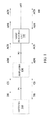
- FIG. 1 is a schematic diagram showing a radio frequency communication system in an embodiment.
- the radio frequency communication system 100 includes an antenna 110, an amplifier 120 and a noise isolating unit 130.
- the antenna 110 receives a wireless signal and transmits a common-mode signal CS and a differential-mode signal DS to the amplifier 120.
- the common-mode signal CS may be a transmission signal related to noise
- the differential-mode signal DS may be a transmission signal related to information.
- the antenna 110 is a single antenna.
- the amplifier 120 is electrically connected to the antenna 110 to amplify the common-mode signal CS and the differential-mode signal DS transmitted by the antenna 110, and output an amplified common-mode signal ACS and an amplified differential-mode signal ADS.
- the differential-mode signal DS and the amplified differential-mode signal ADS are shown in a full line
- the common-mode signal CS and the amplified common-mode signal ACS are shown in a dotted line in FIG. 1 .
- the noise isolating unit 130 is electrically connected to the amplifier 120 to transmit the amplified differential-mode signal ADS and isolate the amplified common-mode signal ACS.
- FIG. 2 is a schematic diagram showing a circuit of a radio frequency communication system in an embodiment.
- the differential-mode signal DS and the amplified differential-mode signal ADS are shown in a full line
- the common-mode signal CS and the amplified common-mode signal ACS are shown in a dotted line in FIG. 2 .
- the amplifier 220 includes a transistor M1.
- a control end of the transistor M1 is electrically connected to the antenna 210, the first end of the transistor M1 is electrically connected to the noise isolating unit 230, and the second end of the transistor M1 is connected to the ground GND.
- the transistor M1 may be a bipolar junction transistor (BJT).
- a base of the transistor M1 is electrically connected to the antenna 210, a collector is electrically connected to the noise isolating unit 230, and an emitter is connected to the ground GND.
- the amplifier 220 in FIG. 2 may be other types of amplifying circuits or elements, which is not limited herein.
- the noise isolating unit 230 includes a first transformer T1 and a second transformer T2.
- the noise isolating unit 230 further includes a first capacitor C1, a second capacitor C2, a third capacitor C3 and a fourth capacitor C4.
- the first transformer T1 includes a first primary winding R1 and a first secondary winding S1.
- One end of the first primary winding R1 is electrically connected to the amplifier 220 via the first capacitor C1, and the other end of the first primary winding R1 is connected to the ground GND.
- One end of the first secondary winding S1 is electrically connected to the second capacitor C2, and the other end of the first secondary winding S1 is electrically connected to the third capacitor C3.
- the second transformer T2 includes a second primary winding R2 and a second secondary winding S2.
- One end of the second primary winding R2 is electrically connected to one end of the first secondary winding S1 via the second capacitor C2, and the other end of the second primary winding R2 is electrically connected to the other end of the first secondary winding S 1 via the third capacitor C3 to isolate the transmission of the amplified common-mode signal ACS.
- one end of the second secondary winding S2 is electrically connected to the fourth capacitor C4, and the other end of the second secondary winding S2 is connected to the ground GND.
- the inductance of the transformer and the capacitance of the capacitors can be obtained by impedance matching in following equations and according to practical requirements.
- XL is an impedance matching value of the radio frequency communication system 100 (such as 50 ⁇ )
- ⁇ is an angular frequency of the operation system
- L is an inductance of the transformer.
- the impedance L can be obtained via the known impedance matching value XL and the known angular frequency ⁇ .
- the capacitance C of the noise isolating unit 130 can be obtained via the known angular frequency ⁇ and the impedance L.
- LTE long term evolution
- the angular frequency ⁇ equals to 2 ⁇ *700MHz
- the impedance matching value XL of the radio frequency system is 50 ⁇ .
- the antenna 210 may be a single-end antenna. Since one end of the single-end antenna is connected to the ground, the single antenna of the antenna 210 can be regarded as a differential antenna according to an image theory, and thus the antenna 210 can transmit the common-mode signal CS and the differential-mode signal DS.
- the common-mode signal CS and the differential-mode signal DS are transmitted to the amplifier 220.
- the amplifier 220 amplifies the common-mode signal CS and the differential-mode signal DS, and outputs the amplified common-mode signal ACS and the amplified differential-mode signal ADS.
- the amplified common-mode signal ACS and the amplified differential-mode signal ADS are inputted to the noise isolating unit 230. Since the amplified common-mode signal ACS is an in-phase signal, it cannot be transmitted in the circuit of the radio frequency communication system 200, and a part of the amplified common-mode signal ACS is isolated by the first transformer T1 and cannot be transmitted to the second transformer T2. On the other hand, since the amplified differential-mode signal ADS is an out of phase signal, it can be transmitted in the circuit of the radio frequency communication system 200, and it can pass through the first transformer T1 and be transmitted to the second transformer T2 completely.
- the rest part of the amplified common-mode signal ACS passes through the first transformer T1 and is inputted to the second transformer T2. Since the amplified common-mode signal ACS is an in-phase signal, the rest part of the amplified common-mode signal ACS is isolated by the second transformer T2 and cannot be outputted. On the other hand, since the amplified differential-mode signal ADS is an out of phase signal, the amplified differential-mode signal ADS can pass through the second transformer T2 completely.
- the first transformer T1 isolates a part of the amplified common-mode signal ACS
- the second transformer T2 isolates the rest part of the amplified common-mode signal ACS.
- the noise isolating unit in the previous embodiment only includes two transformers and four capacitors, which is not limited herein.
- the person with ordinary skills in the art can change the number of transformers and capacitors according to practical requirements, so as to get better noise isolating effect.
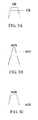
- FIG. 3A is a schematic diagram showing waveforms of the common-mode signal CS and the differential-mode signal DS at a node P1 of the embodiment in FIG. 1 .
- FIG. 3B is a schematic diagram showing waveforms of the amplified common-mode signal ACS and the amplified differential-mode signal ADS at a node P2 of the embodiment in FIG. 1 .
- FIG. 3C is a schematic diagram showing waveforms of the amplified common-mode signal ACS and the amplified differential-mode signal ADS at a node P3 of the embodiment in FIG. 1 .
- the differential-mode signal DS and the amplified differential-mode signal ADS in FIG. 3A to FIG. 3C are shown in a full line
- the common-mode signal CS and the amplified common-mode signal ACS in FIG. 3A to FIG. 3C are shown in a dotted line.
- the node P1 is between the antenna 110 and the amplifier 120
- the node P2 is between the amplifier 120 and the noise isolating unit 130
- the node P3 is behind the noise isolating unit 130.
- the amplified common-mode signal ACS is outputted.
- the differential-mode signal DS is amplified by the amplifier 120 to form the amplified differential-mode signal ADS.
- the amplified common-mode signal ACS and the amplified differential-mode signal ADS are inputted to the noise isolating unit 130, and the noise isolating unit 130 isolates the amplified common-mode signal ACS to reduce the noise signal.
- the amplified differential-mode signal ADS passes through the noise isolating unit 130, its waveform is restored to the waveform which is inputted to the amplifier 120.
- the noise isolating unit 130 can reduce the noise signal and maintain the information signal, and thus it can improve the signal to noise ratio.
- the noise isolating unit 130 which isolates the amplified common-mode signal ACS can be achieved by different means according to practical requirements.
- a layout at a printed circuit board (PCB) can form an equivalent circuit of the noise isolating unit 130.
- the inductance of the transformers and the capacitance of the capacitors can be obtained via the equations in the previous embodiment.
- the equivalent circuit of the noise isolating unit 130 may also be achieved via low temperature co-fired ceramic (LTCC) to isolate the amplified common-mode signal ACS, which is not limited herein.
- LTCC low temperature co-fired ceramic
- FIG. 4 is a flow chart showing a noise isolation method in an embodiment.
- the noise isolation method 400 can be applied to the radio frequency communication system shown in FIG. 2 , which is not limited herein. Please refer to FIG. 2 and FIG. 4 , the noise isolation method 400 includes following steps.
- the antenna 210 transmits the common-mode signal CS (S410).
- the amplifier 220 amplifies the common-mode signal CS and outputs the amplified common-mode signal ACS (S420).
- the noise isolating unit 230 isolates the transmission of the amplified common-mode signal ACS (S430).
- the antenna 210 includes a single antenna.
- the amplifier 220 includes a transistor M1. A control end of the transistor M1 is electrically connected to the antenna 210, the first end of the transistor M1 is electrically connected to the noise isolating unit 230, and the second end of the transistor M1 is connected to the ground GND.
- the noise isolating unit 230 includes a first transformer T1 and a second transformer T2. In another embodiment, the noise isolating unit 230 further includes a first capacitor C1, a second capacitor C2, a third capacitor C3 and a fourth capacitor C4.
- the first transformer T1 includes a first primary winding R1 and a first secondary winding S1.
- One end of the first primary winding R1 is electrically connected to the amplifier 220 via the first capacitor C1, and the other end of the first primary winding R1 is connected to the ground GND.
- One end of the first secondary winding S1 is electrically connected to the second capacitor C2, and the other end of the first secondary winding S1 is electrically connected to the third capacitor C3.
- the second transformer T2 includes a second primary winding R2 and a second secondary winding S2.
- One end of the second primary winding R2 is electrically connected to one end of the first secondary winding S1 via the second capacitor C2, and the other end of the second primary winding R2 is electrically connected to the other end of the first secondary winding S 1 via the third capacitor C3 to isolate the transmission of the amplified common-mode signal ACS.
- one end of the second secondary winding S2 is electrically connected to the fourth capacitor C4, and the other end of the second secondary winding S2 is connected to the ground GND.
- the amplified common-mode signal ACS is an in-phase signal, it cannot be transmitted in the circuit of the radio frequency communication system 200, and a part of the amplified common-mode signal ACS is isolated by the first transformer T1 and cannot be transmitted to the second transformer T2.
- the amplified differential-mode signal ADS is an out of phase signal, it can be transmitted in the circuit of the radio frequency communication system 200, and it can pass through the first transformer T1 and be transmitted to the second transformer T2 completely.
- a rest part of the amplified common-mode signal ACS passes through the first transformer T1 and is inputted to the second transformer T2. Since the amplified common-mode signal ACS is an in-phase signal, the rest part of the amplified common-mode signal ACS is isolated by the second transformer T2 and cannot be outputted. On the other hand, since the amplified differential-mode signal ADS is an out of phase signal, the amplified differential-mode signal ADS can pass through the second transformer T2 completely.
- the sequence of the steps in the noise isolation method 400 shown in FIG. 4 can be adjusted according to practical requirements, and all or a part of the steps can be executed at the same time, which is not limited herein.
- the radio frequency communication system uses the noise isolating unit to isolate the common-mode signal and transmit the differential-mode signal. Moreover, a better noise isolating effect can be obtained by adding transformers and capacitors of the noise isolating unit. Consequently, the radio frequency communication system can effectively reduce the noise and improve the signal to noise ratio without affecting the original information signal.
Landscapes
- Engineering & Computer Science (AREA)
- Power Engineering (AREA)
- Amplifiers (AREA)
- Noise Elimination (AREA)
- Computer Networks & Wireless Communication (AREA)
- Signal Processing (AREA)
- Filters And Equalizers (AREA)
Abstract
A radio frequency communication system and a noise isolation method applied to the radio frequency communication system are provided. The radio frequency communication system includes an antenna, an amplifier and a noise isolating unit. The amplifier is electrically connected to the antenna to amplify a common-mode signal transmitted by the antenna and outputs an amplified common-mode signal. The noise isolating unit is electrically connected to the amplifier to isolate the amplified common-mode signal. The noise isolating unit includes a first transformer and a second transformer. The noise isolating unit isolates the common-mode signal and transmits the differential-mode signal, which can effectively reduce the noise and improve a signal to noise ratio without affecting the original signal.
Description
- The invention relates to a radio frequency communication system and, more particularly, to a radio frequency communication system with a noise isolation circuit.
- As high requirement on electronic products, a communication device for transmitting information becomes more important. Taking a radio frequency (RF) circuit as an example, a radio frequency communication system usually uses an antenna (such a single-end antenna or a differential antenna) to exchange data. However, when the antenna receives or transmits signals, it is easily interfered by electromagnetic noise, and thus the signal outputted by the antenna may be mixed with a lot of noise, which results in a low signal to noise ratio and a signal distortion. The signal distortion may generate an error in the communication device, and the electronic device cannot transmit information correctly.
- A radio frequency communication system and a noise isolation method applied thereto are provided. The radio frequency communication system uses a noise isolating unit which includes a plurality of transformers and capacitors to isolate the noise in the signals received by an antenna, and the radio frequency communication system can improve a signal to noise ratio.
- A radio frequency communication system includes an antenna, an amplifier and a noise isolating unit. The amplifier is electrically connected to the antenna to amplify a common-mode signal transmitted by the antenna and outputs an amplified common-mode signal. The noise isolating unit is electrically connected to the amplifier to isolate the amplified common-mode signal. The noise isolating unit includes a first transformer and a second transformer. The first transformer includes a first primary winding and a first secondary winding, and the first primary winding is electrically connected to the amplifier. The second transformer includes a second primary winding and a second secondary winding, and the second primary winding is electrically connected to the first secondary winding to isolate the transmission of the amplified common-mode signal.
- A noise isolation method applied to a radio frequency communication system is also provided. The radio frequency communication system includes an antenna, an amplifier and a noise isolating unit. The noise isolating unit further includes a first transformer and a second transformer. The first transformer includes a first primary winding and a first secondary winding, and the first primary winding is electrically connected to the amplifier. The second transformer includes a second primary winding and a second secondary winding, and the second primary winding is electrically connected to the first secondary winding. Noise isolation method includes following steps: transmits a common-mode signal by the antenna; amplifies the common-mode signal and outputs the amplified common-mode signal by the amplifier; and isolates the transmission of the amplified common-mode signal by the noise isolating unit.
- These and other features, aspects and advantages of the present invention will become better understood with regard to the following description, appended claims, and accompanying drawings.
-
-
FIG. 1 is a schematic diagram showing a radio frequency communication system in an embodiment; -
FIG. 2 is a schematic diagram showing a circuit of a radio frequency communication system in an embodiment; -
FIG. 3A is a schematic diagram showing waveforms of a common-mode signal CS and a differential-mode signal DS at a node P1 of the embodiment inFIG. 1 ; -
FIG. 3B is a schematic diagram showing waveforms of an amplified common-mode signal ACS and an amplified differential-mode signal ADS at a node P2 of the embodiment inFIG. 1 ; -
FIG. 3C is a schematic diagram showing waveforms of an amplified common-mode signal ACS and an amplified differential-mode signal ADS at a node P3 of the embodiment inFIG. 1 ; and -
FIG. 4 is a flow chart showing a noise isolation method in an embodiment. - "Coupling" or "connecting" means two or more components directly or indirectly contact with each other physically or electrically, and it may also means two or more components cooperate or interact with each other.
-
FIG. 1 is a schematic diagram showing a radio frequency communication system in an embodiment. As shown inFIG. 1 , the radiofrequency communication system 100 includes anantenna 110, anamplifier 120 and anoise isolating unit 130. - One end of the
antenna 110 is electrically connected to theamplifier 120, and the other end is electrically connected to the ground GND. Theantenna 110 receives a wireless signal and transmits a common-mode signal CS and a differential-mode signal DS to theamplifier 120. The common-mode signal CS may be a transmission signal related to noise, and the differential-mode signal DS may be a transmission signal related to information. In an embodiment, theantenna 110 is a single antenna. - The
amplifier 120 is electrically connected to theantenna 110 to amplify the common-mode signal CS and the differential-mode signal DS transmitted by theantenna 110, and output an amplified common-mode signal ACS and an amplified differential-mode signal ADS. In order to show the differential-mode signal and the common-mode signal clearly, the differential-mode signal DS and the amplified differential-mode signal ADS are shown in a full line, the common-mode signal CS and the amplified common-mode signal ACS are shown in a dotted line inFIG. 1 . - The
noise isolating unit 130 is electrically connected to theamplifier 120 to transmit the amplified differential-mode signal ADS and isolate the amplified common-mode signal ACS. -
FIG. 2 is a schematic diagram showing a circuit of a radio frequency communication system in an embodiment. In order to show the differential-mode signal and the common-mode signal clearly, the differential-mode signal DS and the amplified differential-mode signal ADS are shown in a full line, the common-mode signal CS and the amplified common-mode signal ACS are shown in a dotted line inFIG. 2 . - In the embodiment, the
amplifier 220 includes a transistor M1. A control end of the transistor M1 is electrically connected to theantenna 210, the first end of the transistor M1 is electrically connected to thenoise isolating unit 230, and the second end of the transistor M1 is connected to the ground GND. - As shown in
FIG. 2 , the transistor M1 may be a bipolar junction transistor (BJT). A base of the transistor M1 is electrically connected to theantenna 210, a collector is electrically connected to thenoise isolating unit 230, and an emitter is connected to the ground GND. Theamplifier 220 inFIG. 2 may be other types of amplifying circuits or elements, which is not limited herein. - As shown in
FIG. 2 , thenoise isolating unit 230 includes a first transformer T1 and a second transformer T2. In the embodiment, thenoise isolating unit 230 further includes a first capacitor C1, a second capacitor C2, a third capacitor C3 and a fourth capacitor C4. - The first transformer T1 includes a first primary winding R1 and a first secondary winding S1. One end of the first primary winding R1 is electrically connected to the
amplifier 220 via the first capacitor C1, and the other end of the first primary winding R1 is connected to the ground GND. One end of the first secondary winding S1 is electrically connected to the second capacitor C2, and the other end of the first secondary winding S1 is electrically connected to the third capacitor C3. - The second transformer T2 includes a second primary winding R2 and a second secondary winding S2. One end of the second primary winding R2 is electrically connected to one end of the first secondary winding S1 via the second capacitor C2, and the other end of the second primary winding R2 is electrically connected to the other end of the first secondary winding S 1 via the third capacitor C3 to isolate the transmission of the amplified common-mode signal ACS. Moreover, one end of the second secondary winding S2 is electrically connected to the fourth capacitor C4, and the other end of the second secondary winding S2 is connected to the ground GND.
- The inductance of the transformer and the capacitance of the capacitors can be obtained by impedance matching in following equations and according to practical requirements.
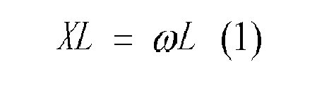

- In the equation (1), XL is an impedance matching value of the radio frequency communication system 100 (such as 50Ω), ω is an angular frequency of the operation system, and L is an inductance of the transformer. As stated above, in the equation (1), the impedance L can be obtained via the known impedance matching value XL and the known angular frequency ω. Then, in the equation (2), the capacitance C of the
noise isolating unit 130 can be obtained via the known angular frequency ω and the impedance L. - For example, in long term evolution (LTE) technology, when the frequency is 700MHz, the angular frequency ω equals to 2π*700MHz, and the impedance matching value XL of the radio frequency system is 50Ω. Thus, the inductance and the capacitance of the
noise isolating unit 130 can be obtained. - In operation, the
antenna 210 may be a single-end antenna. Since one end of the single-end antenna is connected to the ground, the single antenna of theantenna 210 can be regarded as a differential antenna according to an image theory, and thus theantenna 210 can transmit the common-mode signal CS and the differential-mode signal DS. - As shown in
FIG. 2 , the common-mode signal CS and the differential-mode signal DS are transmitted to theamplifier 220. Theamplifier 220 amplifies the common-mode signal CS and the differential-mode signal DS, and outputs the amplified common-mode signal ACS and the amplified differential-mode signal ADS. Then, the amplified common-mode signal ACS and the amplified differential-mode signal ADS are inputted to thenoise isolating unit 230. Since the amplified common-mode signal ACS is an in-phase signal, it cannot be transmitted in the circuit of the radiofrequency communication system 200, and a part of the amplified common-mode signal ACS is isolated by the first transformer T1 and cannot be transmitted to the second transformer T2. On the other hand, since the amplified differential-mode signal ADS is an out of phase signal, it can be transmitted in the circuit of the radiofrequency communication system 200, and it can pass through the first transformer T1 and be transmitted to the second transformer T2 completely. - Furthermore, the rest part of the amplified common-mode signal ACS passes through the first transformer T1 and is inputted to the second transformer T2. Since the amplified common-mode signal ACS is an in-phase signal, the rest part of the amplified common-mode signal ACS is isolated by the second transformer T2 and cannot be outputted. On the other hand, since the amplified differential-mode signal ADS is an out of phase signal, the amplified differential-mode signal ADS can pass through the second transformer T2 completely.
- As stated above, the first transformer T1 isolates a part of the amplified common-mode signal ACS, and the second transformer T2 isolates the rest part of the amplified common-mode signal ACS. Thus, if the number of the transformers and the capacitors of the
noise isolating unit 230 are large, the noise isolating effect is better, the noise is reduced, and the signal to noise ratio is improved more efficiently. - The noise isolating unit in the previous embodiment only includes two transformers and four capacitors, which is not limited herein. The person with ordinary skills in the art can change the number of transformers and capacitors according to practical requirements, so as to get better noise isolating effect.
-
FIG. 3A is a schematic diagram showing waveforms of the common-mode signal CS and the differential-mode signal DS at a node P1 of the embodiment inFIG. 1 .FIG. 3B is a schematic diagram showing waveforms of the amplified common-mode signal ACS and the amplified differential-mode signal ADS at a node P2 of the embodiment inFIG. 1 .FIG. 3C is a schematic diagram showing waveforms of the amplified common-mode signal ACS and the amplified differential-mode signal ADS at a node P3 of the embodiment inFIG. 1 . In order to show the symbols clearly, the differential-mode signal DS and the amplified differential-mode signal ADS inFIG. 3A to FIG. 3C are shown in a full line, and the common-mode signal CS and the amplified common-mode signal ACS inFIG. 3A to FIG. 3C are shown in a dotted line. - Please refer to
FIG. 1 andFIG. 3A to FIG. 3C . As shown inFIG. 1 , the node P1 is between theantenna 110 and theamplifier 120, the node P2 is between theamplifier 120 and thenoise isolating unit 130, and the node P3 is behind thenoise isolating unit 130. - As shown in
FIG. 1 andFIG. 3A to FIG. 3C , after the common-mode signal CS outputted by theantenna 110 passes through theamplifier 120, the amplified common-mode signal ACS is outputted. The differential-mode signal DS is amplified by theamplifier 120 to form the amplified differential-mode signal ADS. Then, the amplified common-mode signal ACS and the amplified differential-mode signal ADS are inputted to thenoise isolating unit 130, and thenoise isolating unit 130 isolates the amplified common-mode signal ACS to reduce the noise signal. Additionally, after the amplified differential-mode signal ADS passes through thenoise isolating unit 130, its waveform is restored to the waveform which is inputted to theamplifier 120. - As shown in
FIG. 3A to FIG. 3C , thenoise isolating unit 130 can reduce the noise signal and maintain the information signal, and thus it can improve the signal to noise ratio. - Furthermore, the
noise isolating unit 130 which isolates the amplified common-mode signal ACS can be achieved by different means according to practical requirements. For example, a layout at a printed circuit board (PCB) can form an equivalent circuit of thenoise isolating unit 130. In the equivalent circuit, the inductance of the transformers and the capacitance of the capacitors can be obtained via the equations in the previous embodiment. The equivalent circuit of thenoise isolating unit 130 may also be achieved via low temperature co-fired ceramic (LTCC) to isolate the amplified common-mode signal ACS, which is not limited herein. -
FIG. 4 is a flow chart showing a noise isolation method in an embodiment. Thenoise isolation method 400 can be applied to the radio frequency communication system shown inFIG. 2 , which is not limited herein. Please refer toFIG. 2 andFIG. 4 , thenoise isolation method 400 includes following steps. - First, the
antenna 210 transmits the common-mode signal CS (S410). Theamplifier 220 amplifies the common-mode signal CS and outputs the amplified common-mode signal ACS (S420). Then, thenoise isolating unit 230 isolates the transmission of the amplified common-mode signal ACS (S430). - In an embodiment, the
antenna 210 includes a single antenna. In another embodiment, theamplifier 220 includes a transistor M1. A control end of the transistor M1 is electrically connected to theantenna 210, the first end of the transistor M1 is electrically connected to thenoise isolating unit 230, and the second end of the transistor M1 is connected to the ground GND. - In an embodiment, the
noise isolating unit 230 includes a first transformer T1 and a second transformer T2. In another embodiment, thenoise isolating unit 230 further includes a first capacitor C1, a second capacitor C2, a third capacitor C3 and a fourth capacitor C4. - The first transformer T1 includes a first primary winding R1 and a first secondary winding S1. One end of the first primary winding R1 is electrically connected to the
amplifier 220 via the first capacitor C1, and the other end of the first primary winding R1 is connected to the ground GND. One end of the first secondary winding S1 is electrically connected to the second capacitor C2, and the other end of the first secondary winding S1 is electrically connected to the third capacitor C3. - The second transformer T2 includes a second primary winding R2 and a second secondary winding S2. One end of the second primary winding R2 is electrically connected to one end of the first secondary winding S1 via the second capacitor C2, and the other end of the second primary winding R2 is electrically connected to the other end of the first secondary winding S 1 via the third capacitor C3 to isolate the transmission of the amplified common-mode signal ACS. Moreover, one end of the second secondary winding S2 is electrically connected to the fourth capacitor C4, and the other end of the second secondary winding S2 is connected to the ground GND.
- In the
noise isolation method 400, since the amplified common-mode signal ACS is an in-phase signal, it cannot be transmitted in the circuit of the radiofrequency communication system 200, and a part of the amplified common-mode signal ACS is isolated by the first transformer T1 and cannot be transmitted to the second transformer T2. On the other hand, since the amplified differential-mode signal ADS is an out of phase signal, it can be transmitted in the circuit of the radiofrequency communication system 200, and it can pass through the first transformer T1 and be transmitted to the second transformer T2 completely. - Furthermore, a rest part of the amplified common-mode signal ACS passes through the first transformer T1 and is inputted to the second transformer T2. Since the amplified common-mode signal ACS is an in-phase signal, the rest part of the amplified common-mode signal ACS is isolated by the second transformer T2 and cannot be outputted. On the other hand, since the amplified differential-mode signal ADS is an out of phase signal, the amplified differential-mode signal ADS can pass through the second transformer T2 completely.
- The sequence of the steps in the
noise isolation method 400 shown inFIG. 4 can be adjusted according to practical requirements, and all or a part of the steps can be executed at the same time, which is not limited herein. - In sum, the radio frequency communication system uses the noise isolating unit to isolate the common-mode signal and transmit the differential-mode signal. Moreover, a better noise isolating effect can be obtained by adding transformers and capacitors of the noise isolating unit. Consequently, the radio frequency communication system can effectively reduce the noise and improve the signal to noise ratio without affecting the original information signal.
Claims (10)
- A radio frequency communication system (100, 200), characterized in that it comprises:an antenna (110, 210);an amplifier (120, 220) electrically connected to the antenna (110, 210) to amplify a common-mode signal (CS) transmitted by the antenna (110, 210) and outputting an amplified common-mode signal (ACS); anda noise isolating unit (130, 230) electrically connected to the amplifier (120, 220) to isolate the amplified common-mode signal (ACS), wherein the noise isolating unit (130, 230) includes:a first transformer (T1) including a first primary winding (R1) and a first secondary winding (S1), wherein the first primary winding (R1) is electrically connected to the amplifier (120, 220); anda second transformer (T2) including a second primary winding (R2) and a second secondary winding (S2), wherein the second primary winding (R2) is electrically connected to the first secondary winding (S1) to isolate the transmission of the amplified common-mode signal (ACS).
- The radio frequency communication system (100, 200) according to claim 1, characterized in that the noise isolating unit (130, 230) further includes:a plurality of capacitors (C1, C2, C3, C4).
- The radio frequency communication system (100, 200) according to claim 2, characterized in that the capacitors (C1, C2, C3, C4) includes a first capacitor (C1), a second capacitor (C2), a third capacitor (C3) and a fourth capacitor (C4);
wherein one end of the first primary winding (R1) is electrically connected to the amplifier (120, 220) via the first capacitor (C1), the other end of the first primary winding (R1) is connected to a ground (GND), one end of the first secondary winding (S1) is electrically connected to the second capacitor (C2), and the other end of the first secondary winding (S1) is electrically connected to the third capacitor (C3); and
one end of the second primary winding (R2) is electrically connected to the second capacitor (C2), the other end of the second primary winding (R2) is electrically connected to the third capacitor (C3), one end of the second secondary winding (S2) is electrically connected to the fourth capacitor (C4), and the other end of the second secondary winding (S2) is connected to the ground (GND). - The radio frequency communication system (100, 200) according to claim 2, characterized in that the first transformer (T1) cooperates with at least one of the capacitors (C1, C2, C3, C4) to isolate the transmission of a part of the amplified common-mode signal (ACS), and the second transformer (T2) cooperates with at least one of the capacitors (C1, C2, C3, C4) to isolate the transmission of the rest part of the amplified common-mode signal (ACS).
- The radio frequency communication system (100, 200) according to claim 1, characterized in that the amplifier (120, 220) is a transistor (M1), a control end of the transistor (M1) is electrically connected to the antenna (110, 210), a first end of the transistor (M1) is electrically connected to the noise isolating unit (130, 230), and a second end of the transistor (M1) is connected to the ground (GND).
- A noise isolation method applied to a radio frequency communication system (100, 200), wherein the radio frequency communication system (100, 200) includes an antenna (110, 210), an amplifier (120, 220) and a noise isolating unit (130, 230), the noise isolating unit (130, 230) includes a first transformer (T1) and a second transformer (T2), the first transformer (T1) includes a first primary winding (R1) and a first secondary winding (S1), the first primary winding (R1) is electrically connected to the amplifier (120, 220), the second transformer (T2) includes a second primary winding (R2) and a second secondary winding (S2), and the second primary winding (R2) is electrically connected to the first secondary winding (S1), the noise isolation method characterized in that it comprises following steps:transmitting a common-mode signal (CS) by the antenna (110, 210);amplifying the common-mode signal (CS) and outputting the amplified common-mode signal (ACS) by the amplifier (120, 220); andisolating the transmission of the amplified common-mode signal (ACS) by the noise isolating unit (130, 230).
- The noise isolation method according to claim 6, characterized in that the noise isolating unit (130, 230) further includes:a plurality of capacitors (C1, C2, C3, C4).
- The noise isolation method according to claim 7, characterized in that the capacitors (C1, C2, C3, C4) includes a first capacitor (C1), a second capacitor (C2), a third capacitor (C3) and a fourth capacitor (C4);
wherein one end of the first primary winding (R1) is electrically connected to the amplifier (120, 220) via the first capacitor (C1), the other end of the first primary winding (R1) is connected to a ground (GND), one end of the first secondary winding (S1) is electrically connected to the second capacitor (C2), and the other end of the first secondary winding (S1) is electrically connected to the third capacitor (C3); and
wherein one end of the second primary winding (R2) is electrically connected to the second capacitor (C2), the other end of the second primary winding (R2) is electrically connected to the third capacitor (C3), one end of the second secondary winding (S2) is electrically connected to the fourth capacitor (C4), and the other end of the second secondary winding (S2) is connected to the ground (GND). - The noise isolation method according to claim 7, characterized in that the step of isolating the transmission of the amplified common-mode signal (ACS) by the noise isolating unit (130, 230) further includes:isolating the transmission of a part of the amplified common-mode signal (ACS) via the cooperation of the first transformer (T1) and at least one of the capacitors (C1, C2, C3, C4); andisolating the transmission of the rest part of the amplified common-mode signal (ACS) via the cooperation of the second transformer (T2) and at least one of the capacitors (C1, C2, C3, C4).
- The noise isolation method according to claim 6, characterized in that the amplifier (120, 220) is a transistor (M1), a control end of the transistor (M1) is electrically connected to the antenna (110, 210), a first end of the transistor (M1) is electrically connected to the noise isolating unit (130, 230), and a second end of the transistor (M1) is connected to the ground (GND).
Applications Claiming Priority (1)
| Application Number | Priority Date | Filing Date | Title |
|---|---|---|---|
| TW102134132A TW201513587A (en) | 2013-09-23 | 2013-09-23 | Radio frequency communication system and noise isolating method using thereof |
Publications (1)
| Publication Number | Publication Date |
|---|---|
| EP2852066A1 true EP2852066A1 (en) | 2015-03-25 |
Family
ID=51751892
Family Applications (1)
| Application Number | Title | Priority Date | Filing Date |
|---|---|---|---|
| EP20140185487 Withdrawn EP2852066A1 (en) | 2013-09-23 | 2014-09-19 | Radio frequency communication system and noise isolation method applied thereto |
Country Status (4)
| Country | Link |
|---|---|
| US (1) | US9425750B2 (en) |
| EP (1) | EP2852066A1 (en) |
| JP (1) | JP2015062268A (en) |
| TW (1) | TW201513587A (en) |
Families Citing this family (1)
| Publication number | Priority date | Publication date | Assignee | Title |
|---|---|---|---|---|
| CN111654784B (en) * | 2020-04-29 | 2024-11-22 | 柏建民 | A method for realizing a universal circuit for direct selection and amplification of weak signals in complex signal environments |
Citations (3)
| Publication number | Priority date | Publication date | Assignee | Title |
|---|---|---|---|---|
| US20050090287A1 (en) * | 2003-10-10 | 2005-04-28 | Ahmadreza (Reza) Rofougaran | RF antenna coupling structure |
| US20110115565A1 (en) * | 2009-11-13 | 2011-05-19 | Qualcomm Incorporated | Cascaded amplifiers with transformer-based bypass mode |
| EP2629434A2 (en) * | 2012-02-17 | 2013-08-21 | Imec | A front-end system for radio devices |
Family Cites Families (10)
| Publication number | Priority date | Publication date | Assignee | Title |
|---|---|---|---|---|
| US3585519A (en) * | 1969-10-16 | 1971-06-15 | Us Navy | Narrow band intermediate frequency amplifier |
| GB2125556A (en) | 1982-08-19 | 1984-03-07 | Gen Electric | Fluid pressure sensor subjected to thermal effect of fluid jets |
| JPS5963540U (en) * | 1982-10-22 | 1984-04-26 | 株式会社東芝 | antenna matching device |
| US6959056B2 (en) * | 2000-06-09 | 2005-10-25 | Bell Canada | RFI canceller using narrowband and wideband noise estimators |
| CN1545340A (en) | 2003-11-13 | 2004-11-10 | 宽讯上线信息科技(上海)有限公司 | Distributed signal covering gain block |
| JP4677845B2 (en) * | 2005-07-27 | 2011-04-27 | 凸版印刷株式会社 | Transport control management system and adapter coil |
| US7378851B1 (en) | 2006-12-11 | 2008-05-27 | General Electric Company | Integrated low noise amplifier and balun for MRI receivers |
| CN101140318B (en) | 2007-10-19 | 2010-07-28 | 大连理工大学 | Resonant RF Magnetic Probe |
| JP4559498B2 (en) * | 2008-02-28 | 2010-10-06 | 株式会社日立製作所 | Active mixer circuit and receiving circuit and millimeter wave communication terminal using the same |
| EP2905900A1 (en) * | 2014-02-11 | 2015-08-12 | Dialog Semiconductor (UK) Limited | Switching control of a bipolar transistor for DCDC power converters |
-
2013
- 2013-09-23 TW TW102134132A patent/TW201513587A/en unknown
- 2013-12-03 JP JP2013250043A patent/JP2015062268A/en active Pending
-
2014
- 2014-09-19 US US14/490,686 patent/US9425750B2/en active Active
- 2014-09-19 EP EP20140185487 patent/EP2852066A1/en not_active Withdrawn
Patent Citations (3)
| Publication number | Priority date | Publication date | Assignee | Title |
|---|---|---|---|---|
| US20050090287A1 (en) * | 2003-10-10 | 2005-04-28 | Ahmadreza (Reza) Rofougaran | RF antenna coupling structure |
| US20110115565A1 (en) * | 2009-11-13 | 2011-05-19 | Qualcomm Incorporated | Cascaded amplifiers with transformer-based bypass mode |
| EP2629434A2 (en) * | 2012-02-17 | 2013-08-21 | Imec | A front-end system for radio devices |
Also Published As
| Publication number | Publication date |
|---|---|
| US9425750B2 (en) | 2016-08-23 |
| JP2015062268A (en) | 2015-04-02 |
| US20150087250A1 (en) | 2015-03-26 |
| TW201513587A (en) | 2015-04-01 |
Similar Documents
| Publication | Publication Date | Title |
|---|---|---|
| CN103957024B (en) | Radio frequency transceiver switch and its working method | |
| EP2629434B1 (en) | A front-end system for radio devices | |
| CN102868419A (en) | Transceiver and integrated circuit | |
| CN103378845B (en) | For flowing the communication interface of electric isolution | |
| US10200091B2 (en) | RF front end module and near field communication device | |
| CN110365372B (en) | Device for Inductively Coupled Communication | |
| CN102577117A (en) | Lr polyphase filter | |
| EP2779439A1 (en) | High-frequency, broadband amplifier circuit | |
| EP2356740A1 (en) | Method and system for amplifying a signal using a transformer matched transistor | |
| EP3930200A1 (en) | Transformer, transmitter circuit, semiconductor chip, semiconductor package, base station, mobile device, and method for a radio frequency transmitter | |
| CN103684289A (en) | Push-pull amplifier and differential push-pull amplifier | |
| US20100197244A1 (en) | Direct coupled radio frequency (RF) transceiver front end | |
| WO2016034740A1 (en) | Iq signal generator system and method | |
| TWI470927B (en) | Differential amplifier with single ended output | |
| CN104009787B (en) | Transmitting device and for analyze amplification transmission signal method | |
| US9813032B2 (en) | Negative impedance circuit | |
| US9425750B2 (en) | Radio frequency communication system and noise isolation method applied thereto | |
| EP2779470B1 (en) | Integrated circuit for transmitting and receiving an RF signal | |
| CN108400791B (en) | Radio frequency transceiver and radio frequency transmitter thereof | |
| JP2021077939A (en) | Power amplifier circuit | |
| JP5743983B2 (en) | Transmission / reception switching circuit, radio apparatus, and transmission / reception switching method | |
| US11038478B2 (en) | Radio frequency signal transceiver | |
| CN104467912B (en) | Radio frequency communication system and noise isolation method applied to the radio frequency communication system | |
| EP3610489B1 (en) | An integrated transformer | |
| US9680527B2 (en) | Radiation hardened 10BASE-T ethernet physical layer (PHY) |
Legal Events
| Date | Code | Title | Description |
|---|---|---|---|
| PUAI | Public reference made under article 153(3) epc to a published international application that has entered the european phase |
Free format text: ORIGINAL CODE: 0009012 |
|
| 17P | Request for examination filed |
Effective date: 20141017 |
|
| AK | Designated contracting states |
Kind code of ref document: A1 Designated state(s): AL AT BE BG CH CY CZ DE DK EE ES FI FR GB GR HR HU IE IS IT LI LT LU LV MC MK MT NL NO PL PT RO RS SE SI SK SM TR |
|
| AX | Request for extension of the european patent |
Extension state: BA ME |
|
| STAA | Information on the status of an ep patent application or granted ep patent |
Free format text: STATUS: THE APPLICATION HAS BEEN WITHDRAWN |
|
| 18W | Application withdrawn |
Effective date: 20150326 |