EP2851955A1 - Procédé de réalisation d'un filtre optique au sein d'un circuit intégré, et circuit intégré correspondant - Google Patents
Procédé de réalisation d'un filtre optique au sein d'un circuit intégré, et circuit intégré correspondant Download PDFInfo
- Publication number
- EP2851955A1 EP2851955A1 EP14184877.0A EP14184877A EP2851955A1 EP 2851955 A1 EP2851955 A1 EP 2851955A1 EP 14184877 A EP14184877 A EP 14184877A EP 2851955 A1 EP2851955 A1 EP 2851955A1
- Authority
- EP
- European Patent Office
- Prior art keywords
- filter layer
- integrated circuit
- substrate
- filter
- photosensitive
- Prior art date
- Legal status (The legal status is an assumption and is not a legal conclusion. Google has not performed a legal analysis and makes no representation as to the accuracy of the status listed.)
- Granted
Links
Images



Classifications
-
- H—ELECTRICITY
- H10—SEMICONDUCTOR DEVICES; ELECTRIC SOLID-STATE DEVICES NOT OTHERWISE PROVIDED FOR
- H10F—INORGANIC SEMICONDUCTOR DEVICES SENSITIVE TO INFRARED RADIATION, LIGHT, ELECTROMAGNETIC RADIATION OF SHORTER WAVELENGTH OR CORPUSCULAR RADIATION
- H10F39/00—Integrated devices, or assemblies of multiple devices, comprising at least one element covered by group H10F30/00, e.g. radiation detectors comprising photodiode arrays
- H10F39/10—Integrated devices
- H10F39/12—Image sensors
- H10F39/18—Complementary metal-oxide-semiconductor [CMOS] image sensors; Photodiode array image sensors
- H10F39/182—Colour image sensors
-
- H—ELECTRICITY
- H10—SEMICONDUCTOR DEVICES; ELECTRIC SOLID-STATE DEVICES NOT OTHERWISE PROVIDED FOR
- H10D—INORGANIC ELECTRIC SEMICONDUCTOR DEVICES
- H10D64/00—Electrodes of devices having potential barriers
- H10D64/60—Electrodes characterised by their materials
- H10D64/66—Electrodes having a conductor capacitively coupled to a semiconductor by an insulator, e.g. MIS electrodes
- H10D64/661—Electrodes having a conductor capacitively coupled to a semiconductor by an insulator, e.g. MIS electrodes the conductor comprising a layer of silicon contacting the insulator, e.g. polysilicon having vertical doping variation
-
- H—ELECTRICITY
- H10—SEMICONDUCTOR DEVICES; ELECTRIC SOLID-STATE DEVICES NOT OTHERWISE PROVIDED FOR
- H10F—INORGANIC SEMICONDUCTOR DEVICES SENSITIVE TO INFRARED RADIATION, LIGHT, ELECTROMAGNETIC RADIATION OF SHORTER WAVELENGTH OR CORPUSCULAR RADIATION
- H10F30/00—Individual radiation-sensitive semiconductor devices in which radiation controls the flow of current through the devices, e.g. photodetectors
- H10F30/20—Individual radiation-sensitive semiconductor devices in which radiation controls the flow of current through the devices, e.g. photodetectors the devices having potential barriers, e.g. phototransistors
- H10F30/21—Individual radiation-sensitive semiconductor devices in which radiation controls the flow of current through the devices, e.g. photodetectors the devices having potential barriers, e.g. phototransistors the devices being sensitive to infrared, visible or ultraviolet radiation
- H10F30/22—Individual radiation-sensitive semiconductor devices in which radiation controls the flow of current through the devices, e.g. photodetectors the devices having potential barriers, e.g. phototransistors the devices being sensitive to infrared, visible or ultraviolet radiation the devices having only one potential barrier, e.g. photodiodes
- H10F30/225—Individual radiation-sensitive semiconductor devices in which radiation controls the flow of current through the devices, e.g. photodetectors the devices having potential barriers, e.g. phototransistors the devices being sensitive to infrared, visible or ultraviolet radiation the devices having only one potential barrier, e.g. photodiodes the potential barrier working in avalanche mode, e.g. avalanche photodiodes
-
- H—ELECTRICITY
- H10—SEMICONDUCTOR DEVICES; ELECTRIC SOLID-STATE DEVICES NOT OTHERWISE PROVIDED FOR
- H10F—INORGANIC SEMICONDUCTOR DEVICES SENSITIVE TO INFRARED RADIATION, LIGHT, ELECTROMAGNETIC RADIATION OF SHORTER WAVELENGTH OR CORPUSCULAR RADIATION
- H10F39/00—Integrated devices, or assemblies of multiple devices, comprising at least one element covered by group H10F30/00, e.g. radiation detectors comprising photodiode arrays
- H10F39/011—Manufacture or treatment of image sensors covered by group H10F39/12
- H10F39/014—Manufacture or treatment of image sensors covered by group H10F39/12 of CMOS image sensors
-
- H—ELECTRICITY
- H10—SEMICONDUCTOR DEVICES; ELECTRIC SOLID-STATE DEVICES NOT OTHERWISE PROVIDED FOR
- H10F—INORGANIC SEMICONDUCTOR DEVICES SENSITIVE TO INFRARED RADIATION, LIGHT, ELECTROMAGNETIC RADIATION OF SHORTER WAVELENGTH OR CORPUSCULAR RADIATION
- H10F39/00—Integrated devices, or assemblies of multiple devices, comprising at least one element covered by group H10F30/00, e.g. radiation detectors comprising photodiode arrays
- H10F39/011—Manufacture or treatment of image sensors covered by group H10F39/12
- H10F39/024—Manufacture or treatment of image sensors covered by group H10F39/12 of coatings or optical elements
-
- H—ELECTRICITY
- H10—SEMICONDUCTOR DEVICES; ELECTRIC SOLID-STATE DEVICES NOT OTHERWISE PROVIDED FOR
- H10F—INORGANIC SEMICONDUCTOR DEVICES SENSITIVE TO INFRARED RADIATION, LIGHT, ELECTROMAGNETIC RADIATION OF SHORTER WAVELENGTH OR CORPUSCULAR RADIATION
- H10F39/00—Integrated devices, or assemblies of multiple devices, comprising at least one element covered by group H10F30/00, e.g. radiation detectors comprising photodiode arrays
- H10F39/10—Integrated devices
- H10F39/12—Image sensors
- H10F39/18—Complementary metal-oxide-semiconductor [CMOS] image sensors; Photodiode array image sensors
- H10F39/184—Infrared image sensors
-
- H—ELECTRICITY
- H10—SEMICONDUCTOR DEVICES; ELECTRIC SOLID-STATE DEVICES NOT OTHERWISE PROVIDED FOR
- H10F—INORGANIC SEMICONDUCTOR DEVICES SENSITIVE TO INFRARED RADIATION, LIGHT, ELECTROMAGNETIC RADIATION OF SHORTER WAVELENGTH OR CORPUSCULAR RADIATION
- H10F39/00—Integrated devices, or assemblies of multiple devices, comprising at least one element covered by group H10F30/00, e.g. radiation detectors comprising photodiode arrays
- H10F39/80—Constructional details of image sensors
- H10F39/803—Pixels having integrated switching, control, storage or amplification elements
- H10F39/8037—Pixels having integrated switching, control, storage or amplification elements the integrated elements comprising a transistor
- H10F39/80373—Pixels having integrated switching, control, storage or amplification elements the integrated elements comprising a transistor characterised by the gate of the transistor
-
- H—ELECTRICITY
- H10—SEMICONDUCTOR DEVICES; ELECTRIC SOLID-STATE DEVICES NOT OTHERWISE PROVIDED FOR
- H10F—INORGANIC SEMICONDUCTOR DEVICES SENSITIVE TO INFRARED RADIATION, LIGHT, ELECTROMAGNETIC RADIATION OF SHORTER WAVELENGTH OR CORPUSCULAR RADIATION
- H10F39/00—Integrated devices, or assemblies of multiple devices, comprising at least one element covered by group H10F30/00, e.g. radiation detectors comprising photodiode arrays
- H10F39/80—Constructional details of image sensors
- H10F39/805—Coatings
- H10F39/8053—Colour filters
-
- H—ELECTRICITY
- H10—SEMICONDUCTOR DEVICES; ELECTRIC SOLID-STATE DEVICES NOT OTHERWISE PROVIDED FOR
- H10F—INORGANIC SEMICONDUCTOR DEVICES SENSITIVE TO INFRARED RADIATION, LIGHT, ELECTROMAGNETIC RADIATION OF SHORTER WAVELENGTH OR CORPUSCULAR RADIATION
- H10F39/00—Integrated devices, or assemblies of multiple devices, comprising at least one element covered by group H10F30/00, e.g. radiation detectors comprising photodiode arrays
- H10F39/80—Constructional details of image sensors
- H10F39/811—Interconnections
Definitions
- the invention relates to integrated circuits and in particular those of imagers type, which comprise photosensitive areas.
- the photosensitive areas of integrated circuits of the imager type can be photodiode substrate regions, in particular photon avalanche photodiodes triggered by an individual photon ("SPAD: Single Photon Avalanche DIODE" in English).
- This type of photodiode is used in particular to detect photons whose wavelength is located in the infrared (around 850 nm). That said, the quantum efficiency of these photodiodes is low for these wavelengths, whereas it is high for the wavelengths of the visible range. The signal-to-noise ratio of these photodiodes can therefore be bad.
- a method for producing an optical filter within an integrated circuit, and an integrated circuit comprising an optical filter which improve the signal-to-noise ratio within photosensitive zones located in substrates, in particular the photosensitive zones of avalanche photodiodes triggered by an individual photon.
- a method of producing an optical filter for filtering radiation within an integrated circuit having a substrate and an interconnect portion above the substrate.
- the embodiment of the filter comprises a formation of at least one filter layer above a photosensitive zone located in the substrate and between the substrate and the interconnection portion, or below the photosensitive zone and opposite the interconnection portion, the product between the thickness of the filter layer and the imaginary part of the refractive index of the filter layer being greater than 1 nanometer for the wavelengths of the radiation to be filtered.
- filtering is meant a reduction in the passage of radiation which is thus blocked.
- the inventors have indeed observed that it was possible to have a filter layer having certain optical properties (in particular a product between the imaginary part of its refractive index and its thickness which has a high value) directly above the zone.
- a filter layer having certain optical properties in particular a product between the imaginary part of its refractive index and its thickness which has a high value
- the product between the thickness of the filter layer and the imaginary part of the refractive index may be greater than 10 nanometers for the wavelengths of the radiation to be filtered.
- An electrically conductive filter layer adapted to be polarized can be formed.
- a conductive filter layer it is particularly advantageous to obtain a conductive filter layer, to be able to polarize this filter layer and improve the electrical behavior of the detection device which comprises the photosensitive zone.
- This filter layer can be connected to said interconnection portion by at least one contact.
- the formation of the at least one filter layer may comprise forming a polycrystalline silicon-containing layer or amorphous silicon.
- the formation of the at least one filter layer may include forming a polycrystalline silicon-containing layer and P-doping of the layer.
- the polycrystalline silicon with a sufficient height (for example 180 nm) and having a P-type doping, has satisfactory optical properties, and possibly polarized.
- said formation of said at least one layer is carried out simultaneously and at the same level as the formation of a gate region of a transistor of the integrated circuit, the filter layer being formed above the photosensitive zone and between the substrate and the interconnection part.
- Integrated circuits generally include transistors having doped polycrystalline silicon gate region, so it is possible to form the filter layer and these gate regions simultaneously. According to one aspect, the invention thus makes it possible to obtain a filter layer without any additional manufacturing step, but simply by modifying the patterns of the photolithography masks used.
- the formation of the photosensitive zone may include the formation of an avalanche photodiode triggered by an individual photon.
- the embodiment of the filter may further comprise forming an additional filter layer located above or inside the interconnection portion if the filter layer is made above the photosensitive area and between the substrate and the substrate. interconnection portion, or made below the filter layer if the filter layer is made below the photosensitive zone and opposite the interconnection portion.
- a method for producing an integrated circuit comprising an embodiment within the integrated circuit of an optical filter according to the method as defined above.
- an integrated circuit comprising a substrate, an interconnection portion above the substrate and an optical filter for filtering radiation.
- the optical filter comprises at least one filter layer, advantageously electrically conductive and adapted to be polarized, located above a photosensitive zone located in the substrate and between the substrate and the part of the substrate. interconnection, or located below the photosensitive zone and opposite the interconnection portion, the product between the thickness of the filter layer and the imaginary part of the refractive index of the filter layer being greater than at 1 nanometer for the wavelengths of the radiation to be filtered.
- the product between the thickness of the filter layer and the imaginary portion of the refractive index may be greater than 10 nanometers for the wavelengths of the radiation to be filtered.
- the electrically conductive filter layer may be connected to said interconnection portion by at least one contact.
- the filter layer may contain polycrystalline silicon or amorphous silicon.
- the filter layer may contain polycrystalline silicon having P-type doping.
- the integrated circuit may furthermore comprise at least one transistor whose gate region comprises polycrystalline silicon having a P-type doping and the same thickness as the filter, the filter layer and the gate region being located at the same level, the filter layer being located above the photosensitive area and between the substrate and the interconnection portion.
- the photosensitive zone may be a photosensitive zone of avalanche photodiode triggered by an individual photon.
- the integrated circuit may further comprise an additional filter layer located above or inside the interconnection portion if the filter layer is located above the photosensitive area and between the substrate and the interconnection portion, or located below the filter layer if the filter layer is located below the photosensitive zone and opposite the interconnection portion.
- a substrate SUB for example made of silicon, in which a photosensitive zone ZP has already been formed.
- the photosensitive area ZP may be part of an avalanche photodiode triggered by an individual photon, or a photodiode designated as the "pinned diode".
- the photosensitive zone ZP may be intended to detect photons having a wavelength located in the infrared, and it is therefore preferable to block the visible domain radiation so that they do not reach this zone. photosensitive.
- zone ZP is a photosensitive zone of imager known as "front face”.
- front face a photosensitive zone of imager
- rear-facing illumination imager a photosensitive zone of imager
- a CF filter layer can be formed above the photosensitive zone ZP.
- This filter layer CF may be a polycrystalline silicon layer having a P-type doping. At the same time, it may also have formed a transistor gate region RG TR on the substrate SUB. As a result, the formation of the filter layer may comprise the same steps as the formation of a transistor gate. Generally, the transistor gates have thicknesses of the order of 180 nm, and this thickness makes it possible to obtain a filter layer adapted to filter radiation from the visible range. The product between the thickness of the filter layer and the imaginary part of the refractive index of this filter layer is here greater than 1 nanometer or even 10 nanometers for the wavelengths of the radiation to be blocked, which corresponds to good absorption.
- amorphous silicon layer having a thickness equal to 180 nanometers (imaginary part of the refractive index equal to 0.5), there is a product at 500 nanometers equal to 90 nanometers, which corresponds to an attenuation of about 90%.
- ES spacers are formed on either side of the gate region RG and also in the vicinity of the edges of the filter layer CF.
- the ITC interconnection region (commonly referred to by the person skilled in the art under the acronym BEOL: Back End Of Line) comprises a plurality of LM metal lines, but it is preferable that no LM metal line extends above the ZP photosensitive area.
- the CF filter layer extends laterally beyond the photosensitive zone ZP, and an electrical contact CT has been formed to connect this filter layer to the interconnection network ITC. With the contact CT, it is possible to polarize the filter layer CF and thus obtain an improved operation for the photosensitive zone ZP.
- the CF filter layer may be supplemented with an additional layer of CSF filter located above or inside the ITC interconnect portion, as shown in FIG. figure 4 .
- the additional CSF filter layer may be a multilayer optical filter stack, or a resin layer.
- This multilayer optical filter may be a multilayer optical filter comprising metal layers and layers of dielectric material.
- an additional filter layer comprising two copper layers having a thickness of about 25 nanometers separated by a nitride layer silicon having a thickness of about 180 nanometers. Silicon nitride layers may also be formed around the copper layers to improve the adhesion of the copper layers and to protect them.
- FIG. 5 there is shown a variant of the invention in which a filter layer CF 'is produced below a photosensitive zone ZP of a substrate SUB and opposite the interconnection portion ITC. An illumination imager is thus obtained from the rear face.
- the filter layer CF ' is made under the substrate SUB. It is also possible to form, under the filter layer CF ', an ARC antireflection layer for example made of silicon nitride, an insulating layer CIS for example made of silicon dioxide and an additional layer of lower filter CIF, for example a multilayer optical filter. Finally, it is possible to produce, under the additional layer of lower filter, an optical lens.
- the CF 'layer may be polycrystalline silicon or preferably amorphous silicon.
- additional filtering is obtained which does not require any additional manufacturing step, and which can improve the diffusion of the electrons in the underlying substrate.
- radiation can be filtered for back-illuminated imagers.
Landscapes
- Solid State Image Pick-Up Elements (AREA)
Abstract
Description
- L'invention concerne les circuits intégrés et notamment ceux de type imageurs, qui comprennent des zones photosensibles.
- Les zones photosensibles de circuits intégrés de type imageurs peuvent être des régions de substrat de photodiodes, notamment des photodiodes à avalanche déclenchée par un photon individuel (« SPAD : Single Photon Avalanche DIODE » en langue anglaise).
- On utilise notamment ce type de photodiode pour détecter des photons dont la longueur d'onde est située dans l'infrarouge (autour de 850 nm). Cela étant, l'efficacité quantique de ces photodiodes est faible pour ces longueurs d'onde, alors qu'elle est élevée pour les longueurs d'onde du domaine visible. Le rapport signal sur bruit de ces photodiodes peut donc être mauvais.
- Il a donc été proposé d'utiliser des filtres pour diminuer la détection des rayonnements du domaine visible qui peuvent être considérés comme du bruit pour le fonctionnement des photodiodes à avalanche déclenchées par un photon individuel. Cela étant, ces filtres ne sont pas toujours suffisamment performants.
- Selon un mode de mise en oeuvre et de réalisation, il est proposé un procédé de réalisation d'un filtre optique au sein d'un circuit intégré, et un circuit intégré comprenant un filtre optique, qui améliorent le rapport signal sur bruit au sein de zones photosensibles situées dans des substrats, en particulier les zones photosensibles de photodiodes à avalanche déclenchée par un photon individuel.
- Selon un aspect, il est proposé un procédé de réalisation d'un filtre optique destiné à filtrer des rayonnements au sein d'un circuit intégré comportant un substrat et une partie d'interconnexion au dessus du substrat.
- Selon une caractéristique générale de cet aspect, la réalisation du filtre comprend une formation d'au moins une couche de filtre au-dessus d'une zone photosensible située dans le substrat et entre le substrat et la partie d'interconnexion, ou en dessous de la zone photosensible et à l'opposé de la partie d'interconnexion, le produit entre l'épaisseur de la couche de filtre et la partie imaginaire de l'indice de réfraction de la couche de filtre étant supérieur à 1 nanomètre pour les longueurs d'ondes des rayonnements à filtrer.
- Par filtrer, on entend une réduction du passage des rayonnements qui sont donc bloqués. A titre d'exemple, on peut souhaiter filtrer le rayonnement correspondant au domaine visible pour détecter des rayonnements infrarouges.
- Les inventeurs ont en effet observé qu'il était possible de disposer une couche de filtre ayant certaines propriétés optiques (en particulier un produit entre la partie imaginaire de son indice de réfraction et son épaisseur qui a une valeur élevée) directement au dessus de la zone photosensible du substrat, avant la formation de la partie d'interconnexion, ou au dos du substrat, par exemple pour un imageur à illumination par la face arrière.
- On peut ainsi bloquer certains rayonnements, en particulier les rayonnements du domaine visible lorsque l'on souhaite détecter des rayonnements infrarouges.
- De préférence, le produit entre l'épaisseur de la couche de filtre et la partie imaginaire de l'indice de réfraction peut être supérieur à 10 nanomètres pour les longueurs d'ondes des rayonnements à filtrer.
- On peut former une couche de filtre électriquement conductrice et adaptée à être polarisée.
- Pour certaines applications, il est particulièrement intéressant d'obtenir une couche de filtre conductrice, pour pouvoir polariser cette couche de filtre et améliorer le comportement électrique du dispositif de détection qui comprend la zone photosensible. On pourra notamment ainsi améliorer la diffusion des électrons dans le substrat.
- On peut connecter cette couche de filtre à ladite partie d'interconnexion par au moins un contact.
- La formation de ladite au moins une couche de filtre peut comprendre une formation d'une couche contenant du silicium polycristallin ou encore du silicium amorphe.
- La formation de ladite au moins une couche de filtre peut comprendre une formation d'une couche contenant du silicium polycristallin et un dopage de type P de la couche.
- Le silicium polycristallin, avec une hauteur suffisante (par exemple 180 nm) et ayant un dopage de type P, a des propriétés optiques satisfaisantes, et peut-être polarisé.
- La formation de ladite au moins une couche est effectuée simultanément et au même niveau que la formation d'une région de grille d'un transistor du circuit intégré, la couche de filtre étant réalisée au dessus de la zone photosensible et entre le substrat et la partie d'interconnexion.
- Les circuits intégrés comprennent généralement des transistors munis de région de grille en silicium polycristallin dopé, il est donc possible de former la couche de filtre et ces régions de grille simultanément. Selon un aspect, l'invention permet donc d'obtenir une couche de filtre sans aucune étape de fabrication supplémentaire, mais simplement en modifiant les motifs des masques de photolithographie utilisés.
- La formation de la zone photosensible peut comprendre la formation d'une photodiode à avalanche déclenchée par un photon individuel.
- La réalisation du filtre peut comprendre en outre une formation d'une couche supplémentaire de filtre située au dessus ou à l'intérieur de la partie d'interconnexion si la couche de filtre est réalisée au dessus de la zone photosensible et entre le substrat et la partie d'interconnexion, ou réalisée en dessous de la couche de filtre si la couche de filtre est réalisée en dessous de la zone photosensible et à l'opposée de la partie d'interconnexion.
- En effet, on pourra également utiliser un filtre selon l'art antérieur pour compléter le filtrage.
- Selon un autre aspect, il est proposé un procédé de réalisation d'un circuit intégré comprenant une réalisation au sein du circuit intégré, d'un filtre optique selon le procédé tel que défini ci-avant.
- Selon un autre aspect, il est proposé un circuit intégré comportant un substrat, une partie d'interconnexion au dessus du substrat et un filtre optique destiné à filtrer des rayonnements.
- Selon une caractéristique générale de cet autre aspect, le filtre optique comprend au moins une couche de filtre, avantageusement électriquement conductrice et adaptée à être polarisée, située au dessus d'une zone photosensible située dans le substrat et entre le substrat et la partie d'interconnexion, ou située en dessous de la zone photosensible et à l'opposé de la partie d'interconnexion, le produit entre l'épaisseur de la couche de filtre et la partie imaginaire de l'indice de réfraction de la couche de filtre étant supérieur à 1 nanomètre pour les longueurs d'ondes des rayonnements à filtrer.
- Pour filtrer une longueur d'onde de l'ordre de 500 nanomètres (rayonnement visible), on peut utiliser une couche de silicium polycristallin ayant une épaisseur de 180 nanomètres et une valeur de partie imaginaire de l'indice de réfraction égale à 0,14. Le produit de l'épaisseur et de la partie imaginaire est alors égal à 25 nanomètres, ce qui permet de diminuer l'intensité lumineuse à 500 nanomètres d'environ 46%.
- Le produit entre l'épaisseur de la couche de filtre et la partie imaginaire de l'indice de réfraction peut être supérieur à 10 nanomètres pour les longueurs d'ondes des rayonnements à filtrer.
- La couche de filtre électriquement conductrice peut être connectée à ladite partie d'interconnexion par au moins un contact.
- La couche de filtre peut contenir du silicium polycristallin ou du silicium amorphe.
- La couche de filtre peut contenir du silicium polycristallin ayant un dopage de type P.
- Le circuit intégré peut comprendre en outre au moins un transistor dont la région de grille comprend du silicium polycristallin ayant un dopage de type P et la même épaisseur que la couche de filtre, la couche de filtre et la région de grille étant situées au même niveau, la couche de filtre étant située au dessus de la zone photosensible et entre le substrat et la partie d'interconnexion.
- La zone photosensible peut être une zone photosensible de photodiode à avalanche déclenchée par un photon individuel.
- Le circuit intégré peut comprendre en outre une couche supplémentaire de filtre située au dessus ou à l'intérieur de la partie d'interconnexion si la couche de filtre est située au dessus de la zone photosensible et entre le substrat et la partie d'interconnexion, ou située en dessous de la couche de filtre si la couche de filtre est située en dessous de la zone photosensible et à l'opposé de la partie d'interconnexion.
- D'autres avantages et caractéristiques de l'invention apparaîtront à l'étude de la description détaillée de modes de mise en oeuvre et de réalisation, pris à titre d'exemple non limitatifs et illustrés par les dessins annexés sur lesquels :
- les
figures 1 à 4 illustrent différentes étapes d'un mode de mise en oeuvre d'un procédé selon l'invention. - Sur la
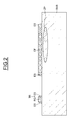
figure 1 , on a représenté un substrat SUB, par exemple en silicium, dans lequel on a déjà formé une zone photosensible ZP. - La zone photosensible ZP peut faire partie d'une photodiode à avalanche déclenchée par un photon individuel, ou encore d'une photodiode désignée sous l'expression anglo-saxonne « pinned diode ».
- À titre indicatif, la zone photosensible ZP peut-être destinée à détecter des photons ayant une longueur d'onde située dans l'infrarouge, et il est donc préférable de bloquer les rayonnements du domaine visible pour qu'ils n'atteignent pas cette zone photosensible.
- Il convient de noter que la zone ZP est une zone photosensible d'imageur dit « face avant ». En variante, il est possible de mettre en oeuvre l'invention au sein d'un imageur à illumination face arrière
- Pour bloquer ces rayonnements, on peut former une couche de filtre CF au dessus de la zone photosensible ZP.
- Cette couche de filtre CF peut être une couche en silicium polycristallin ayant un dopage de type P. Simultanément, on peut également avoir formé une région de grille RG de transistor TR sur le substrat SUB. De ce fait, la formation de la couche de filtre peut comprendre les mêmes étapes que la formation d'une grille de transistor. Généralement, les grilles de transistor ont des épaisseurs de l'ordre de 180 nm, et cette épaisseur permet d'obtenir une couche de filtre adapté pour filtrer les rayonnements du domaine visible. Le produit entre l'épaisseur de la couche de filtre et la partie imaginaire de l'indice de réfraction de cette couche de filtre est ici supérieur à 1 nanomètre voire à 10 nanomètres pour les longueurs d'ondes des rayonnements à bloquer, ce qui correspond à une bonne absorption.
- A titre d'exemple, pour une épaisseur de silicium polycristallin de 180 nanomètres, (avec une partie imaginaire de l'indice de réfraction égale à 0.054 pour la longueur d'onde de 600 nm), on a un produit (domaine visible à filtrer) de l'ordre de 9.7 nanomètres, ce qui correspond à une atténuation de l'intensité lumineuse à 600 nanomètres reçue de l'ordre de 18% environ. Une même couche de silicium polycristallin a, au voisinage d'une longueur d'onde de 850 nanomètres à laisser passer, un produit de l'ordre de 0.7 nanomètres (avec une partie imaginaire de l'indice de réfraction égale à 0.004), ce qui correspond à une atténuation très faible de 1% environ.
- Pour une couche de silicium amorphe ayant une épaisseur égale à 180 nanomètres (partie imaginaire de l'indice de réfraction égale à 0.5), on a un produit à 500 nanomètres égal à 90 nanomètres, ce qui correspond à une atténuation de 90% environ.
- On peut noter que des espaceurs ES sont formés de part et d'autre de la région de grille RG et également au voisinage des bords de la couche de filtre CF.
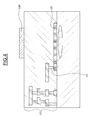
- On peut ensuite former une région d'interconnexion ITC au dessus du substrat sur lequel on a formé la couche de filtre CF et le transistor TR, comme illustré sur la
figure 3 . - La région d'interconnexion ITC (communément désignée par l'homme du métier sous l'acronyme anglo-saxon « BEOL : Back End Of Line ») comprend une pluralité de lignes métalliques LM, mais il est préférable qu'aucune ligne métallique LM ne s'étende au-dessus de la zone photosensible ZP.
- La couche de filtre CF s'étend latéralement au-delà de la zone photosensible ZP, et un contact électrique CT a été formé pour connecter cette couche de filtre au réseau d'interconnexion ITC. Avec le contact CT, on peut polariser la couche de filtre CF et ainsi obtenir un fonctionnement amélioré pour la zone photosensible ZP.
- En effet en polarisant la couche de filtre CF par un contact électrique, on vient créer un champ électrique qui crée une zone d'accumulation de trous sous l'interface du silicium cristallin. De ce fait on s'affranchit des défauts de surface, ce qui permet de diminuer le « DCR » (« Dark Count Rate ») pour un capteur à photon unique de type SPAD ou le courant d'obscurité pour un imageur, et cela sans dégrader l'efficacité quantique (QE : Quantum Efficiency) des pixels.
- Bien que cela ne soit pas obligatoire, la couche de filtre CF peut-être complétée par une couche supplémentaire de filtre CSF située au-dessus ou à l'intérieur de la partie d'interconnexion ITC, comme illustré sur la
figure 4 . - La couche supplémentaire de filtre CSF peut être un empilement de filtre optique multicouche, ou encore une couche de résine. Ce filtre optique multicouche peut être un filtre optique multicouche comprenant des couches de métal et des couches de matériau diélectrique. A titre indicatif, pour transmettre une longueur d'onde de 850 nanomètres et bloquer les rayonnements dans le domaine visible, on peut utiliser une couche supplémentaire de filtre comportant deux couches de cuivre ayant une épaisseur d'environ 25 nanomètres séparées par une couche de nitrure de silicium ayant une épaisseur d'environ 180 nanomètres. On pourra également former des couches de nitrure de silicium autour des couches de cuivre pour améliorer l'adhérence des couches de cuivre et les protéger.
- Sur la
figure 5 , on a représenté une variante de l'invention dans laquelle une couche de filtre CF' est réalisée en dessous d'une zone photosensible ZP d'un substrat SUB et à l'opposé de la partie d'interconnexion ITC. On obtient ainsi un imageur à illumination par la face arrière. - Comme illustré sur la
figure 5 , la couche de filtre CF' est réalisée sous le substrat SUB. On peut également former, sous la couche de filtre CF', une couche antireflet ARC par exemple en nitrure de silicium, une couche isolante CIS par exemple en dioxyde de silicium et une couche supplémentaire de filtre inférieure CIF, par exemple un filtre optique multicouche. Enfin, on peut réaliser, sous la couche supplémentaire de filtre inférieure, une lentille optique. - On obtient ainsi, avec la couche CF', une bonne atténuation des rayonnements à filtrer. La couche CF' peut être en silicium polycristallin ou préférentiellement en silicium amorphe.
- Selon un aspect de l'invention, on obtient un meilleur fonctionnement des circuits intégrés comprenant des zones photosensibles, c'est-à-dire des circuits intégrés imageurs.
- Selon un aspect de l'invention, on obtient un filtrage supplémentaire qui ne nécessite aucune étape de fabrication supplémentaire, et qui peut améliorer la diffusion des électrons dans le substrat sous-jacent.
- Selon encore un autre aspect de l'invention, on peut filtrer des rayonnements pour les imageurs à illumination face arrière.
Claims (17)
- Procédé de réalisation d'un filtre optique destiné à filtrer des rayonnements au sein d'un circuit intégré comportant un substrat (SUB) et une partie d'interconnexion (ITC) au dessus du substrat, caractérisé en ce que la réalisation du filtre comprend une formation d'au moins une couche de filtre électriquement conductrice adaptée à être polarisée (CF) au-dessus d'une zone photosensible (ZP) située dans le substrat et entre le substrat et la partie d'interconnexion, ou en dessous de la zone photosensible et à l'opposé de la partie d'interconnexion, le produit entre l'épaisseur de la couche de filtre (CF) et la partie imaginaire de l'indice de réfraction de la couche de filtre (CF) étant supérieur à 1 nanomètre pour les longueurs d'ondes des rayonnements à filtrer.
- Procédé selon la revendication 1, dans lequel le produit entre l'épaisseur de la couche de filtre et la partie imaginaire de l'indice de réfraction est supérieur à 10 nanomètres pour les longueurs d'onde des rayonnements à filtrer.
- Procédé selon la revendication 1 ou 2, dans lequel on connecte ladite couche de filtre électriquement conductrice (CF) à ladite partie d'interconnexion (ITC) par au moins un contact.
- Procédé selon l'une quelconque des revendications précédentes, dans lequel la formation de ladite au moins une couche de filtre comprend une formation d'une couche contenant du silicium polycristallin ou du silicium amorphe.
- Procédé selon la revendication 4, dans lequel la formation de ladite au moins une couche de filtre comprend une formation d'une couche contenant du silicium polycristallin et un dopage de type P de la couche.
- Procédé selon la revendication 4, dans lequel la formation de ladite au moins une couche est effectuée simultanément et au même niveau que la formation d'une région de grille (RG) d'un transistor (TR) du circuit intégré, la couche de filtre étant réalisée au dessus de la zone photosensible et entre le substrat et la partie d'interconnexion.
- Procédé selon l'une quelconque des revendications précédentes, dans lequel la formation de la zone photosensible comprend la formation d'une photodiode à avalanche déclenchée par un photon individuel.
- Procédé selon l'une quelconque des revendications précédentes, dans lequel la réalisation du filtre comprend en outre une formation d'une couche supplémentaire de filtre (CSF) située au dessus ou à l'intérieur de la partie d'interconnexion si la couche de filtre est réalisée au dessus de la zone photosensible et entre le substrat et la partie d'interconnexion, ou réalisée en dessous de la couche de filtre si la couche de filtre est réalisée en dessous de la zone photosensible et à l'opposé de la partie d'interconnexion.
- Procédé de réalisation d'un circuit intégré comprenant une réalisation au sein du circuit intégré, d'un filtre optique selon le procédé selon l'une des revendications 1 à 8.
- Circuit intégré comportant un substrat (SUB), une partie d'interconnexion (ITC) au dessus du substrat et un filtre optique destiné à filtrer des rayonnements, caractérisé en ce que le filtre optique comprend au moins une couche de filtre électriquement conductrice adaptée à être polarisée (CF) située au dessus d'une zone photosensible (ZP) située dans le substrat et entre le substrat et la partie d'interconnexion, ou située en dessous de la zone photosensible et à l'opposé de la partie d'interconnexion, le produit entre l'épaisseur de la couche de filtre et la partie imaginaire de l'indice de réfraction de la couche de filtre étant supérieur à 1 nanomètre pour les longueurs d'ondes des rayonnements à filtrer.
- Circuit intégré selon la revendication 10, dans lequel le produit entre l'épaisseur de la couche de filtre et la partie imaginaire de l'indice de réfraction est supérieur à 10 nanomètres pour les longueurs d'ondes des rayonnements à filtrer.
- Circuit intégré selon la revendication 10 ou 11, comprenant au moins un contact connectant la couche de filtre électriquement conductrice (CF) à ladite partie d'interconnexion (ITC).
- Circuit intégré selon l'une quelconque des revendications 10 à 12, dans lequel la couche de filtre contient du silicium polycristallin ou du silicium amorphe.
- Circuit intégré selon la revendication 13, dans lequel la couche de filtre contient du silicium polycristallin ayant un dopage de type P.
- Circuit intégré selon la revendication 14, comprenant en outre au moins un transistor (TR) dont la région de grille (RG) comprend du silicium polycristallin ayant un dopage de type P et la même épaisseur que la couche de filtre, la couche de filtre et la région de grille étant situées au même niveau, la couche de filtre étant située au dessus de la zone photosensible et entre le substrat et la partie d'interconnexion.
- Circuit intégré selon l'une quelconque des revendications 10 à 15, dans lequel la zone photosensible est une zone photosensible de photodiode à avalanche déclenchée par un photon individuel.
- Circuit intégré selon l'une quelconque des revendications 10 à 16, comprenant en outre une couche supplémentaire de filtre (CSF) située au dessus ou à l'intérieur de la partie d'interconnexion si la couche de filtre est située au dessus de la zone photosensible et entre le substrat et la partie d'interconnexion, ou située en dessous de la couche de filtre si la couche de filtre est située en dessous de la zone photosensible et à l'opposé de la partie d'interconnexion.
Applications Claiming Priority (1)
| Application Number | Priority Date | Filing Date | Title |
|---|---|---|---|
| FR1359026A FR3010829B1 (fr) | 2013-09-19 | 2013-09-19 | Procede de realisation d'un filtre optique au sein d'un circuit integre, et circuit integre correspondant |
Publications (2)
| Publication Number | Publication Date |
|---|---|
| EP2851955A1 true EP2851955A1 (fr) | 2015-03-25 |
| EP2851955B1 EP2851955B1 (fr) | 2022-06-22 |
Family
ID=49949816
Family Applications (1)
| Application Number | Title | Priority Date | Filing Date |
|---|---|---|---|
| EP14184877.0A Active EP2851955B1 (fr) | 2013-09-19 | 2014-09-16 | Procédé de réalisation d'un filtre optique au sein d'un circuit intégré, et circuit intégré correspondant |
Country Status (3)
| Country | Link |
|---|---|
| US (1) | US9219095B2 (fr) |
| EP (1) | EP2851955B1 (fr) |
| FR (1) | FR3010829B1 (fr) |
Cited By (1)
| Publication number | Priority date | Publication date | Assignee | Title |
|---|---|---|---|---|
| FR3036849A1 (fr) * | 2015-05-28 | 2016-12-02 | Commissariat Energie Atomique | Procede de realisation d'un filtre infrarouge associe a un capteur d'image |
Families Citing this family (4)
| Publication number | Priority date | Publication date | Assignee | Title |
|---|---|---|---|---|
| CN105334666A (zh) * | 2015-12-04 | 2016-02-17 | 江苏日久光电股份有限公司 | 高透过型光学组合薄膜 |
| CN105301844A (zh) * | 2015-12-04 | 2016-02-03 | 江苏日久光电股份有限公司 | 一种高透过型光学组合薄膜 |
| EP3416197A4 (fr) * | 2016-02-08 | 2019-06-12 | Panasonic Intellectual Property Management Co., Ltd. | Élément de conversion de longueur d'onde et dispositif de source de lumière |
| CN115832067A (zh) * | 2022-12-30 | 2023-03-21 | 苏州如涵科技有限公司 | 半导体结构及装置 |
Citations (2)
| Publication number | Priority date | Publication date | Assignee | Title |
|---|---|---|---|---|
| US20090298220A1 (en) * | 2007-09-06 | 2009-12-03 | International Business Machines Corporation | Imagers having electrically active optical elements |
| US20120267694A1 (en) * | 2011-04-19 | 2012-10-25 | Infineon Technologies Ag | Integrated circuit arrangements |
Family Cites Families (12)
| Publication number | Priority date | Publication date | Assignee | Title |
|---|---|---|---|---|
| US7601236B2 (en) * | 2003-11-28 | 2009-10-13 | Semiconductor Energy Laboratory Co., Ltd. | Method of manufacturing display device |
| AT505987B1 (de) * | 2007-11-07 | 2011-01-15 | Arc Austrian Res Centers Gmbh | Qkd-einrichtung |
| JP5305387B2 (ja) * | 2007-12-25 | 2013-10-02 | セイコーインスツル株式会社 | 光検出装置、及び画像表示装置 |
| US8629981B2 (en) * | 2008-02-01 | 2014-01-14 | Palo Alto Research Center Incorporated | Analyzers with time variation based on color-coded spatial modulation |
| US8361371B2 (en) * | 2008-02-08 | 2013-01-29 | Molecular Imprints, Inc. | Extrusion reduction in imprint lithography |
| US7759755B2 (en) * | 2008-05-14 | 2010-07-20 | International Business Machines Corporation | Anti-reflection structures for CMOS image sensors |
| US20110275538A1 (en) * | 2008-08-25 | 2011-11-10 | Tufts University | Measurement of biological targets |
| JP2012151210A (ja) * | 2011-01-18 | 2012-08-09 | Sony Corp | 半導体レーザ素子 |
| WO2013008765A1 (fr) * | 2011-07-08 | 2013-01-17 | Semiconductor Energy Laboratory Co., Ltd. | Module électroluminescent, dispositif électroluminescent et procédé de fabrication du module électroluminescent |
| US8723140B2 (en) * | 2011-08-09 | 2014-05-13 | Palo Alto Research Center Incorporated | Particle analyzer with spatial modulation and long lifetime bioprobes |
| US9170371B2 (en) * | 2012-04-24 | 2015-10-27 | Hewlett-Packard Development Company, L.P. | Micro-ring optical resonators |
| US20140001588A1 (en) * | 2012-06-28 | 2014-01-02 | Intersil Americas LLC | Optical sensors devices including a hybrid of wafer-level inorganic dielectric and organic color filters |
-
2013
- 2013-09-19 FR FR1359026A patent/FR3010829B1/fr not_active Expired - Fee Related
-
2014
- 2014-09-16 EP EP14184877.0A patent/EP2851955B1/fr active Active
- 2014-09-18 US US14/489,698 patent/US9219095B2/en active Active
Patent Citations (2)
| Publication number | Priority date | Publication date | Assignee | Title |
|---|---|---|---|---|
| US20090298220A1 (en) * | 2007-09-06 | 2009-12-03 | International Business Machines Corporation | Imagers having electrically active optical elements |
| US20120267694A1 (en) * | 2011-04-19 | 2012-10-25 | Infineon Technologies Ag | Integrated circuit arrangements |
Cited By (2)
| Publication number | Priority date | Publication date | Assignee | Title |
|---|---|---|---|---|
| FR3036849A1 (fr) * | 2015-05-28 | 2016-12-02 | Commissariat Energie Atomique | Procede de realisation d'un filtre infrarouge associe a un capteur d'image |
| EP3098851A3 (fr) * | 2015-05-28 | 2017-02-15 | Commissariat A L'energie Atomique Et Aux Energies Alternatives | Procédé de réalisation d'un filtre infrarouge associé à un capteur d'image |
Also Published As
| Publication number | Publication date |
|---|---|
| FR3010829A1 (fr) | 2015-03-20 |
| EP2851955B1 (fr) | 2022-06-22 |
| FR3010829B1 (fr) | 2017-01-27 |
| US9219095B2 (en) | 2015-12-22 |
| US20150076573A1 (en) | 2015-03-19 |
Similar Documents
| Publication | Publication Date | Title |
|---|---|---|
| EP3503192B1 (fr) | Dispositif d'acquisition d'une image 2d et d'une image de profondeur d'une scène | |
| EP3185294B1 (fr) | Dispositif optoelectronique d'emission de lumiere | |
| EP2851955B1 (fr) | Procédé de réalisation d'un filtre optique au sein d'un circuit intégré, et circuit intégré correspondant | |
| EP2636068B1 (fr) | Imageur monolithique multispectral visible et infrarouge | |
| EP2786411A1 (fr) | Dispositif a matrice de diodes a resistance d'acces et stabilite amelioree | |
| FR2954587A1 (fr) | Procede de formation d'un capteur d'images eclaire par la face arriere | |
| EP2732473A1 (fr) | Matrice de photodiodes ingaas | |
| EP2786412A1 (fr) | Bloc detecteur optique | |
| FR3100926A1 (fr) | Capteur d'images réalisé en technologie 3D séquentielle | |
| EP3098851B1 (fr) | Procédé de réalisation d'un filtre infrarouge associé à un capteur d'image | |
| FR3123151A1 (fr) | Procédé de fabrication d'un dispositif optoélectronique | |
| EP3326027A1 (fr) | Filtre et detecteur optiques a nanoparticules ou microparticules resonantes | |
| WO2013189997A1 (fr) | Structure semiconductrice comportant une zone absorbante placee dans une cavite focalisante | |
| FR3040536A1 (fr) | Capteur d'image a diaphotie spectrale et optique reduite | |
| EP2337076A1 (fr) | Dispositif microélectronique, en particulier capteur d'image à illumination par la face arrière et procédé de fabrication. | |
| EP1432044A1 (fr) | Photodiode à filtre en polysilicium intégré | |
| EP4268281B1 (fr) | Intégration d'un circuit de détection à base de résonateurs optiques interconnectés sur un circuit de lecture d'un imageur | |
| EP2835671B1 (fr) | Procédé de réalisation d'un filtre optique multicouches épais au sein d'un circuit intégré, et circuit intégré comprenant un filtre optique multicouches épais | |
| FR3083001A1 (fr) | Capteur d'images | |
| FR3014243A1 (fr) | Procede de realisation d'un dispositif imageur integre a illumination face avant comportant au moins un filtre optique metallique, et dispositif correspondant | |
| WO2022128873A1 (fr) | Filtre angulaire optique | |
| FR3087939A1 (fr) | Capteur de lumiere | |
| EP4362093A1 (fr) | Dispositif emetteur et recepteur de lumiere | |
| FR3014245A1 (fr) | Procede de formation d'un dispositif integre a illumination face arriere comprenant un filtre optique metallique, et dispositif correspondant | |
| FR3163770A1 (fr) | Dispositif électronique ayant des pixels à base de boîtes quantiques |
Legal Events
| Date | Code | Title | Description |
|---|---|---|---|
| PUAI | Public reference made under article 153(3) epc to a published international application that has entered the european phase |
Free format text: ORIGINAL CODE: 0009012 |
|
| 17P | Request for examination filed |
Effective date: 20140916 |
|
| AK | Designated contracting states |
Kind code of ref document: A1 Designated state(s): AL AT BE BG CH CY CZ DE DK EE ES FI FR GB GR HR HU IE IS IT LI LT LU LV MC MK MT NL NO PL PT RO RS SE SI SK SM TR |
|
| AX | Request for extension of the european patent |
Extension state: BA ME |
|
| R17P | Request for examination filed (corrected) |
Effective date: 20150914 |
|
| 17Q | First examination report despatched |
Effective date: 20160113 |
|
| RIN1 | Information on inventor provided before grant (corrected) |
Inventor name: JOUAN, SEBASTIEN Inventor name: MARTY, MICHEL Inventor name: FREY, LAURENT |
|
| STAA | Information on the status of an ep patent application or granted ep patent |
Free format text: STATUS: EXAMINATION IS IN PROGRESS |
|
| GRAP | Despatch of communication of intention to grant a patent |
Free format text: ORIGINAL CODE: EPIDOSNIGR1 |
|
| STAA | Information on the status of an ep patent application or granted ep patent |
Free format text: STATUS: GRANT OF PATENT IS INTENDED |
|
| INTG | Intention to grant announced |
Effective date: 20210916 |
|
| GRAJ | Information related to disapproval of communication of intention to grant by the applicant or resumption of examination proceedings by the epo deleted |
Free format text: ORIGINAL CODE: EPIDOSDIGR1 |
|
| STAA | Information on the status of an ep patent application or granted ep patent |
Free format text: STATUS: EXAMINATION IS IN PROGRESS |
|
| INTC | Intention to grant announced (deleted) | ||
| GRAP | Despatch of communication of intention to grant a patent |
Free format text: ORIGINAL CODE: EPIDOSNIGR1 |
|
| STAA | Information on the status of an ep patent application or granted ep patent |
Free format text: STATUS: GRANT OF PATENT IS INTENDED |
|
| INTG | Intention to grant announced |
Effective date: 20220126 |
|
| GRAS | Grant fee paid |
Free format text: ORIGINAL CODE: EPIDOSNIGR3 |
|
| GRAA | (expected) grant |
Free format text: ORIGINAL CODE: 0009210 |
|
| STAA | Information on the status of an ep patent application or granted ep patent |
Free format text: STATUS: THE PATENT HAS BEEN GRANTED |
|
| AK | Designated contracting states |
Kind code of ref document: B1 Designated state(s): AL AT BE BG CH CY CZ DE DK EE ES FI FR GB GR HR HU IE IS IT LI LT LU LV MC MK MT NL NO PL PT RO RS SE SI SK SM TR |
|
| REG | Reference to a national code |
Ref country code: GB Ref legal event code: FG4D Free format text: NOT ENGLISH |
|
| REG | Reference to a national code |
Ref country code: CH Ref legal event code: EP |
|
| REG | Reference to a national code |
Ref country code: DE Ref legal event code: R096 Ref document number: 602014084080 Country of ref document: DE |
|
| REG | Reference to a national code |
Ref country code: AT Ref legal event code: REF Ref document number: 1500344 Country of ref document: AT Kind code of ref document: T Effective date: 20220715 |
|
| REG | Reference to a national code |
Ref country code: IE Ref legal event code: FG4D Free format text: LANGUAGE OF EP DOCUMENT: FRENCH |
|
| REG | Reference to a national code |
Ref country code: LT Ref legal event code: MG9D |
|
| REG | Reference to a national code |
Ref country code: NL Ref legal event code: MP Effective date: 20220622 |
|
| PG25 | Lapsed in a contracting state [announced via postgrant information from national office to epo] |
Ref country code: SE Free format text: LAPSE BECAUSE OF FAILURE TO SUBMIT A TRANSLATION OF THE DESCRIPTION OR TO PAY THE FEE WITHIN THE PRESCRIBED TIME-LIMIT Effective date: 20220622 Ref country code: NO Free format text: LAPSE BECAUSE OF FAILURE TO SUBMIT A TRANSLATION OF THE DESCRIPTION OR TO PAY THE FEE WITHIN THE PRESCRIBED TIME-LIMIT Effective date: 20220922 Ref country code: LT Free format text: LAPSE BECAUSE OF FAILURE TO SUBMIT A TRANSLATION OF THE DESCRIPTION OR TO PAY THE FEE WITHIN THE PRESCRIBED TIME-LIMIT Effective date: 20220622 Ref country code: HR Free format text: LAPSE BECAUSE OF FAILURE TO SUBMIT A TRANSLATION OF THE DESCRIPTION OR TO PAY THE FEE WITHIN THE PRESCRIBED TIME-LIMIT Effective date: 20220622 Ref country code: GR Free format text: LAPSE BECAUSE OF FAILURE TO SUBMIT A TRANSLATION OF THE DESCRIPTION OR TO PAY THE FEE WITHIN THE PRESCRIBED TIME-LIMIT Effective date: 20220923 Ref country code: FI Free format text: LAPSE BECAUSE OF FAILURE TO SUBMIT A TRANSLATION OF THE DESCRIPTION OR TO PAY THE FEE WITHIN THE PRESCRIBED TIME-LIMIT Effective date: 20220622 Ref country code: BG Free format text: LAPSE BECAUSE OF FAILURE TO SUBMIT A TRANSLATION OF THE DESCRIPTION OR TO PAY THE FEE WITHIN THE PRESCRIBED TIME-LIMIT Effective date: 20220922 |
|
| REG | Reference to a national code |
Ref country code: AT Ref legal event code: MK05 Ref document number: 1500344 Country of ref document: AT Kind code of ref document: T Effective date: 20220622 |
|
| PG25 | Lapsed in a contracting state [announced via postgrant information from national office to epo] |
Ref country code: RS Free format text: LAPSE BECAUSE OF FAILURE TO SUBMIT A TRANSLATION OF THE DESCRIPTION OR TO PAY THE FEE WITHIN THE PRESCRIBED TIME-LIMIT Effective date: 20220622 Ref country code: LV Free format text: LAPSE BECAUSE OF FAILURE TO SUBMIT A TRANSLATION OF THE DESCRIPTION OR TO PAY THE FEE WITHIN THE PRESCRIBED TIME-LIMIT Effective date: 20220622 |
|
| PG25 | Lapsed in a contracting state [announced via postgrant information from national office to epo] |
Ref country code: NL Free format text: LAPSE BECAUSE OF FAILURE TO SUBMIT A TRANSLATION OF THE DESCRIPTION OR TO PAY THE FEE WITHIN THE PRESCRIBED TIME-LIMIT Effective date: 20220622 |
|
| PG25 | Lapsed in a contracting state [announced via postgrant information from national office to epo] |
Ref country code: SM Free format text: LAPSE BECAUSE OF FAILURE TO SUBMIT A TRANSLATION OF THE DESCRIPTION OR TO PAY THE FEE WITHIN THE PRESCRIBED TIME-LIMIT Effective date: 20220622 Ref country code: SK Free format text: LAPSE BECAUSE OF FAILURE TO SUBMIT A TRANSLATION OF THE DESCRIPTION OR TO PAY THE FEE WITHIN THE PRESCRIBED TIME-LIMIT Effective date: 20220622 Ref country code: RO Free format text: LAPSE BECAUSE OF FAILURE TO SUBMIT A TRANSLATION OF THE DESCRIPTION OR TO PAY THE FEE WITHIN THE PRESCRIBED TIME-LIMIT Effective date: 20220622 Ref country code: PT Free format text: LAPSE BECAUSE OF FAILURE TO SUBMIT A TRANSLATION OF THE DESCRIPTION OR TO PAY THE FEE WITHIN THE PRESCRIBED TIME-LIMIT Effective date: 20221024 Ref country code: ES Free format text: LAPSE BECAUSE OF FAILURE TO SUBMIT A TRANSLATION OF THE DESCRIPTION OR TO PAY THE FEE WITHIN THE PRESCRIBED TIME-LIMIT Effective date: 20220622 Ref country code: EE Free format text: LAPSE BECAUSE OF FAILURE TO SUBMIT A TRANSLATION OF THE DESCRIPTION OR TO PAY THE FEE WITHIN THE PRESCRIBED TIME-LIMIT Effective date: 20220622 Ref country code: CZ Free format text: LAPSE BECAUSE OF FAILURE TO SUBMIT A TRANSLATION OF THE DESCRIPTION OR TO PAY THE FEE WITHIN THE PRESCRIBED TIME-LIMIT Effective date: 20220622 Ref country code: AT Free format text: LAPSE BECAUSE OF FAILURE TO SUBMIT A TRANSLATION OF THE DESCRIPTION OR TO PAY THE FEE WITHIN THE PRESCRIBED TIME-LIMIT Effective date: 20220622 |
|
| PG25 | Lapsed in a contracting state [announced via postgrant information from national office to epo] |
Ref country code: PL Free format text: LAPSE BECAUSE OF FAILURE TO SUBMIT A TRANSLATION OF THE DESCRIPTION OR TO PAY THE FEE WITHIN THE PRESCRIBED TIME-LIMIT Effective date: 20220622 Ref country code: IS Free format text: LAPSE BECAUSE OF FAILURE TO SUBMIT A TRANSLATION OF THE DESCRIPTION OR TO PAY THE FEE WITHIN THE PRESCRIBED TIME-LIMIT Effective date: 20221022 |
|
| REG | Reference to a national code |
Ref country code: DE Ref legal event code: R097 Ref document number: 602014084080 Country of ref document: DE |
|
| PG25 | Lapsed in a contracting state [announced via postgrant information from national office to epo] |
Ref country code: AL Free format text: LAPSE BECAUSE OF FAILURE TO SUBMIT A TRANSLATION OF THE DESCRIPTION OR TO PAY THE FEE WITHIN THE PRESCRIBED TIME-LIMIT Effective date: 20220622 |
|
| PG25 | Lapsed in a contracting state [announced via postgrant information from national office to epo] |
Ref country code: MC Free format text: LAPSE BECAUSE OF FAILURE TO SUBMIT A TRANSLATION OF THE DESCRIPTION OR TO PAY THE FEE WITHIN THE PRESCRIBED TIME-LIMIT Effective date: 20220622 Ref country code: DK Free format text: LAPSE BECAUSE OF FAILURE TO SUBMIT A TRANSLATION OF THE DESCRIPTION OR TO PAY THE FEE WITHIN THE PRESCRIBED TIME-LIMIT Effective date: 20220622 |
|
| PLBE | No opposition filed within time limit |
Free format text: ORIGINAL CODE: 0009261 |
|
| REG | Reference to a national code |
Ref country code: CH Ref legal event code: PL |
|
| STAA | Information on the status of an ep patent application or granted ep patent |
Free format text: STATUS: NO OPPOSITION FILED WITHIN TIME LIMIT |
|
| REG | Reference to a national code |
Ref country code: BE Ref legal event code: MM Effective date: 20220930 |
|
| 26N | No opposition filed |
Effective date: 20230323 |
|
| PG25 | Lapsed in a contracting state [announced via postgrant information from national office to epo] |
Ref country code: LU Free format text: LAPSE BECAUSE OF NON-PAYMENT OF DUE FEES Effective date: 20220916 |
|
| PG25 | Lapsed in a contracting state [announced via postgrant information from national office to epo] |
Ref country code: LI Free format text: LAPSE BECAUSE OF NON-PAYMENT OF DUE FEES Effective date: 20220930 Ref country code: IE Free format text: LAPSE BECAUSE OF NON-PAYMENT OF DUE FEES Effective date: 20220916 Ref country code: CH Free format text: LAPSE BECAUSE OF NON-PAYMENT OF DUE FEES Effective date: 20220930 |
|
| PG25 | Lapsed in a contracting state [announced via postgrant information from national office to epo] |
Ref country code: SI Free format text: LAPSE BECAUSE OF FAILURE TO SUBMIT A TRANSLATION OF THE DESCRIPTION OR TO PAY THE FEE WITHIN THE PRESCRIBED TIME-LIMIT Effective date: 20220622 |
|
| PG25 | Lapsed in a contracting state [announced via postgrant information from national office to epo] |
Ref country code: BE Free format text: LAPSE BECAUSE OF NON-PAYMENT OF DUE FEES Effective date: 20220930 |
|
| PG25 | Lapsed in a contracting state [announced via postgrant information from national office to epo] |
Ref country code: IT Free format text: LAPSE BECAUSE OF FAILURE TO SUBMIT A TRANSLATION OF THE DESCRIPTION OR TO PAY THE FEE WITHIN THE PRESCRIBED TIME-LIMIT Effective date: 20220622 |
|
| PG25 | Lapsed in a contracting state [announced via postgrant information from national office to epo] |
Ref country code: HU Free format text: LAPSE BECAUSE OF FAILURE TO SUBMIT A TRANSLATION OF THE DESCRIPTION OR TO PAY THE FEE WITHIN THE PRESCRIBED TIME-LIMIT; INVALID AB INITIO Effective date: 20140916 |
|
| PG25 | Lapsed in a contracting state [announced via postgrant information from national office to epo] |
Ref country code: CY Free format text: LAPSE BECAUSE OF FAILURE TO SUBMIT A TRANSLATION OF THE DESCRIPTION OR TO PAY THE FEE WITHIN THE PRESCRIBED TIME-LIMIT Effective date: 20220622 |
|
| PG25 | Lapsed in a contracting state [announced via postgrant information from national office to epo] |
Ref country code: MK Free format text: LAPSE BECAUSE OF FAILURE TO SUBMIT A TRANSLATION OF THE DESCRIPTION OR TO PAY THE FEE WITHIN THE PRESCRIBED TIME-LIMIT Effective date: 20220622 |
|
| PG25 | Lapsed in a contracting state [announced via postgrant information from national office to epo] |
Ref country code: MT Free format text: LAPSE BECAUSE OF FAILURE TO SUBMIT A TRANSLATION OF THE DESCRIPTION OR TO PAY THE FEE WITHIN THE PRESCRIBED TIME-LIMIT Effective date: 20220622 |
|
| PG25 | Lapsed in a contracting state [announced via postgrant information from national office to epo] |
Ref country code: BG Free format text: LAPSE BECAUSE OF FAILURE TO SUBMIT A TRANSLATION OF THE DESCRIPTION OR TO PAY THE FEE WITHIN THE PRESCRIBED TIME-LIMIT Effective date: 20220622 |
|
| REG | Reference to a national code |
Ref country code: DE Ref legal event code: R079 Ref document number: 602014084080 Country of ref document: DE Free format text: PREVIOUS MAIN CLASS: H01L0027146000 Ipc: H10F0039180000 |
|
| PG25 | Lapsed in a contracting state [announced via postgrant information from national office to epo] |
Ref country code: BG Free format text: LAPSE BECAUSE OF FAILURE TO SUBMIT A TRANSLATION OF THE DESCRIPTION OR TO PAY THE FEE WITHIN THE PRESCRIBED TIME-LIMIT Effective date: 20220622 |
|
| PGFP | Annual fee paid to national office [announced via postgrant information from national office to epo] |
Ref country code: DE Payment date: 20250916 Year of fee payment: 12 |
|
| PGFP | Annual fee paid to national office [announced via postgrant information from national office to epo] |
Ref country code: GB Payment date: 20250919 Year of fee payment: 12 |
|
| PGFP | Annual fee paid to national office [announced via postgrant information from national office to epo] |
Ref country code: FR Payment date: 20250929 Year of fee payment: 12 |
|
| PG25 | Lapsed in a contracting state [announced via postgrant information from national office to epo] |
Ref country code: TR Free format text: LAPSE BECAUSE OF FAILURE TO SUBMIT A TRANSLATION OF THE DESCRIPTION OR TO PAY THE FEE WITHIN THE PRESCRIBED TIME-LIMIT Effective date: 20220622 |