EP2850635B1 - Ladungsträger-lithografiesystem mit mehreren teilstrahlen und kühlanordnungsherstellungsverfahren - Google Patents
Ladungsträger-lithografiesystem mit mehreren teilstrahlen und kühlanordnungsherstellungsverfahren Download PDFInfo
- Publication number
- EP2850635B1 EP2850635B1 EP13722748.4A EP13722748A EP2850635B1 EP 2850635 B1 EP2850635 B1 EP 2850635B1 EP 13722748 A EP13722748 A EP 13722748A EP 2850635 B1 EP2850635 B1 EP 2850635B1
- Authority
- EP
- European Patent Office
- Prior art keywords
- cooling
- plate
- beamlet
- cooling channels
- apertures
- Prior art date
- Legal status (The legal status is an assumption and is not a legal conclusion. Google has not performed a legal analysis and makes no representation as to the accuracy of the status listed.)
- Active
Links
- 238000001816 cooling Methods 0.000 title claims description 223
- 239000002245 particle Substances 0.000 title claims description 44
- 238000001459 lithography Methods 0.000 title claims description 39
- 238000004519 manufacturing process Methods 0.000 title claims description 11
- 239000000110 cooling liquid Substances 0.000 claims description 26
- 238000009826 distribution Methods 0.000 claims description 18
- 238000012546 transfer Methods 0.000 claims description 18
- 238000000034 method Methods 0.000 claims description 15
- 239000012790 adhesive layer Substances 0.000 claims description 12
- 239000002826 coolant Substances 0.000 claims description 9
- 239000010936 titanium Substances 0.000 claims description 9
- XLYOFNOQVPJJNP-UHFFFAOYSA-N water Substances O XLYOFNOQVPJJNP-UHFFFAOYSA-N 0.000 claims description 9
- RTAQQCXQSZGOHL-UHFFFAOYSA-N Titanium Chemical compound [Ti] RTAQQCXQSZGOHL-UHFFFAOYSA-N 0.000 claims description 8
- 229910052719 titanium Inorganic materials 0.000 claims description 8
- 238000000059 patterning Methods 0.000 claims description 4
- 238000003466 welding Methods 0.000 claims description 4
- 239000012809 cooling fluid Substances 0.000 description 50
- 239000000463 material Substances 0.000 description 12
- 230000003287 optical effect Effects 0.000 description 10
- 239000012530 fluid Substances 0.000 description 7
- QGZKDVFQNNGYKY-UHFFFAOYSA-N Ammonia Chemical compound N QGZKDVFQNNGYKY-UHFFFAOYSA-N 0.000 description 6
- 238000010894 electron beam technology Methods 0.000 description 6
- 235000012431 wafers Nutrition 0.000 description 6
- 239000010949 copper Substances 0.000 description 5
- RYGMFSIKBFXOCR-UHFFFAOYSA-N Copper Chemical compound [Cu] RYGMFSIKBFXOCR-UHFFFAOYSA-N 0.000 description 4
- XUIMIQQOPSSXEZ-UHFFFAOYSA-N Silicon Chemical compound [Si] XUIMIQQOPSSXEZ-UHFFFAOYSA-N 0.000 description 4
- 238000003491 array Methods 0.000 description 4
- 229910052802 copper Inorganic materials 0.000 description 4
- 238000010438 heat treatment Methods 0.000 description 4
- 239000010410 layer Substances 0.000 description 4
- 229910052710 silicon Inorganic materials 0.000 description 4
- 239000010703 silicon Substances 0.000 description 4
- 238000011144 upstream manufacturing Methods 0.000 description 4
- GYHNNYVSQQEPJS-UHFFFAOYSA-N Gallium Chemical compound [Ga] GYHNNYVSQQEPJS-UHFFFAOYSA-N 0.000 description 3
- 229910021529 ammonia Inorganic materials 0.000 description 3
- 230000008901 benefit Effects 0.000 description 3
- PMHQVHHXPFUNSP-UHFFFAOYSA-M copper(1+);methylsulfanylmethane;bromide Chemical compound Br[Cu].CSC PMHQVHHXPFUNSP-UHFFFAOYSA-M 0.000 description 3
- 229910052733 gallium Inorganic materials 0.000 description 3
- 239000000853 adhesive Substances 0.000 description 2
- 230000001070 adhesive effect Effects 0.000 description 2
- 230000000295 complement effect Effects 0.000 description 2
- 238000010586 diagram Methods 0.000 description 2
- 238000007599 discharging Methods 0.000 description 2
- 239000007788 liquid Substances 0.000 description 2
- 239000013307 optical fiber Substances 0.000 description 2
- 239000004065 semiconductor Substances 0.000 description 2
- 239000000126 substance Substances 0.000 description 2
- WFKWXMTUELFFGS-UHFFFAOYSA-N tungsten Chemical compound [W] WFKWXMTUELFFGS-UHFFFAOYSA-N 0.000 description 2
- 229910052721 tungsten Inorganic materials 0.000 description 2
- 239000010937 tungsten Substances 0.000 description 2
- PIGFYZPCRLYGLF-UHFFFAOYSA-N Aluminum nitride Chemical compound [Al]#N PIGFYZPCRLYGLF-UHFFFAOYSA-N 0.000 description 1
- 230000008859 change Effects 0.000 description 1
- 238000006243 chemical reaction Methods 0.000 description 1
- 239000011248 coating agent Substances 0.000 description 1
- 238000000576 coating method Methods 0.000 description 1
- 239000004020 conductor Substances 0.000 description 1
- 238000005260 corrosion Methods 0.000 description 1
- 230000007797 corrosion Effects 0.000 description 1
- 238000013500 data storage Methods 0.000 description 1
- 230000008021 deposition Effects 0.000 description 1
- 238000013461 design Methods 0.000 description 1
- 238000009792 diffusion process Methods 0.000 description 1
- 238000006073 displacement reaction Methods 0.000 description 1
- 238000000609 electron-beam lithography Methods 0.000 description 1
- 230000003628 erosive effect Effects 0.000 description 1
- 238000005530 etching Methods 0.000 description 1
- 238000002474 experimental method Methods 0.000 description 1
- 239000000835 fiber Substances 0.000 description 1
- 230000003993 interaction Effects 0.000 description 1
- 230000002452 interceptive effect Effects 0.000 description 1
- 238000010884 ion-beam technique Methods 0.000 description 1
- 238000005304 joining Methods 0.000 description 1
- 229910001338 liquidmetal Inorganic materials 0.000 description 1
- 235000015250 liver sausages Nutrition 0.000 description 1
- 238000007726 management method Methods 0.000 description 1
- 230000007246 mechanism Effects 0.000 description 1
- 238000012986 modification Methods 0.000 description 1
- 230000004048 modification Effects 0.000 description 1
- 238000000206 photolithography Methods 0.000 description 1
- 230000008569 process Effects 0.000 description 1
- 238000005086 pumping Methods 0.000 description 1
- 230000005855 radiation Effects 0.000 description 1
- 230000001172 regenerating effect Effects 0.000 description 1
- 238000007711 solidification Methods 0.000 description 1
- 230000008023 solidification Effects 0.000 description 1
Images


Classifications
-
- H—ELECTRICITY
- H01—ELECTRIC ELEMENTS
- H01J—ELECTRIC DISCHARGE TUBES OR DISCHARGE LAMPS
- H01J37/00—Discharge tubes with provision for introducing objects or material to be exposed to the discharge, e.g. for the purpose of examination or processing thereof
- H01J37/02—Details
- H01J37/04—Arrangements of electrodes and associated parts for generating or controlling the discharge, e.g. electron-optical arrangement, ion-optical arrangement
- H01J37/045—Beam blanking or chopping, i.e. arrangements for momentarily interrupting exposure to the discharge
-
- B—PERFORMING OPERATIONS; TRANSPORTING
- B82—NANOTECHNOLOGY
- B82Y—SPECIFIC USES OR APPLICATIONS OF NANOSTRUCTURES; MEASUREMENT OR ANALYSIS OF NANOSTRUCTURES; MANUFACTURE OR TREATMENT OF NANOSTRUCTURES
- B82Y10/00—Nanotechnology for information processing, storage or transmission, e.g. quantum computing or single electron logic
-
- B—PERFORMING OPERATIONS; TRANSPORTING
- B82—NANOTECHNOLOGY
- B82Y—SPECIFIC USES OR APPLICATIONS OF NANOSTRUCTURES; MEASUREMENT OR ANALYSIS OF NANOSTRUCTURES; MANUFACTURE OR TREATMENT OF NANOSTRUCTURES
- B82Y40/00—Manufacture or treatment of nanostructures
-
- H—ELECTRICITY
- H01—ELECTRIC ELEMENTS
- H01J—ELECTRIC DISCHARGE TUBES OR DISCHARGE LAMPS
- H01J37/00—Discharge tubes with provision for introducing objects or material to be exposed to the discharge, e.g. for the purpose of examination or processing thereof
- H01J37/30—Electron-beam or ion-beam tubes for localised treatment of objects
- H01J37/317—Electron-beam or ion-beam tubes for localised treatment of objects for changing properties of the objects or for applying thin layers thereon, e.g. for ion implantation
- H01J37/3174—Particle-beam lithography, e.g. electron beam lithography
- H01J37/3177—Multi-beam, e.g. fly's eye, comb probe
-
- H—ELECTRICITY
- H01—ELECTRIC ELEMENTS
- H01J—ELECTRIC DISCHARGE TUBES OR DISCHARGE LAMPS
- H01J2237/00—Discharge tubes exposing object to beam, e.g. for analysis treatment, etching, imaging
- H01J2237/002—Cooling arrangements
-
- H—ELECTRICITY
- H01—ELECTRIC ELEMENTS
- H01J—ELECTRIC DISCHARGE TUBES OR DISCHARGE LAMPS
- H01J2237/00—Discharge tubes exposing object to beam, e.g. for analysis treatment, etching, imaging
- H01J2237/04—Means for controlling the discharge
- H01J2237/043—Beam blanking
- H01J2237/0435—Multi-aperture
- H01J2237/0437—Semiconductor substrate
-
- H—ELECTRICITY
- H01—ELECTRIC ELEMENTS
- H01J—ELECTRIC DISCHARGE TUBES OR DISCHARGE LAMPS
- H01J2237/00—Discharge tubes exposing object to beam, e.g. for analysis treatment, etching, imaging
- H01J2237/04—Means for controlling the discharge
- H01J2237/045—Diaphragms
- H01J2237/0451—Diaphragms with fixed aperture
- H01J2237/0453—Diaphragms with fixed aperture multiple apertures
-
- H—ELECTRICITY
- H01—ELECTRIC ELEMENTS
- H01J—ELECTRIC DISCHARGE TUBES OR DISCHARGE LAMPS
- H01J2237/00—Discharge tubes exposing object to beam, e.g. for analysis treatment, etching, imaging
- H01J2237/30—Electron or ion beam tubes for processing objects
- H01J2237/317—Processing objects on a microscale
- H01J2237/3175—Lithography
- H01J2237/31774—Multi-beam
-
- H—ELECTRICITY
- H01—ELECTRIC ELEMENTS
- H01J—ELECTRIC DISCHARGE TUBES OR DISCHARGE LAMPS
- H01J2237/00—Discharge tubes exposing object to beam, e.g. for analysis treatment, etching, imaging
- H01J2237/30—Electron or ion beam tubes for processing objects
- H01J2237/317—Processing objects on a microscale
- H01J2237/3175—Lithography
- H01J2237/31793—Problems associated with lithography
- H01J2237/31794—Problems associated with lithography affecting masks
Definitions
- the present invention relates to a charged particle multi-beamlet lithography system.
- the invention further relates to manufacturing a cooling arrangement for use within such lithography system.
- Lithography is a critical part of such manufacturing process.
- lithography systems use a light beam and mask as a means to reproduce pattern data for exposing a target, such as a wafer with a coating of resist thereon.
- charged particle beamlets may be used to transfer a pattern onto such target. The beamlets may be individually controllable to obtain the desired pattern.
- charged particle lithography systems For such charged particle lithography systems to be commercially viable, they need to handle a certain minimum throughput, i.e. the number of wafer being processed per hour should not be too far below the number of wafers per hour that are currently processed with an optical lithography system. Furthermore, the charged particle lithography systems need to meet low error margins. The combination of a relatively high throughput in combination with the requirement to meet low error margins is challenging.
- a higher throughput may be obtained by using more beamlets, and therefore more current.
- handling a greater number of beamlets results in the need for more control circuitry.
- an increase in the current results in more charged particles that interact with components in the lithography system.
- Both the circuitry and the impingement of charged particles onto components may cause heating of the respective components within the lithography system. Such heating may reduce the accuracy of the patterning process within the lithography system. In a worst case scenario, such heating may stop one or more components within the lithography system from functioning.
- Japanese patent document JP2006140267 discloses a charged particle multi beam exposure device in which the thermal load of an aperture array under irradiation of electron beam is reduced for improved precision in lithography.
- the invention provides a charged particle multi-beamlet lithography system for exposing a target using a plurality of charged particle beamlets according to claim 1.
- the system comprising: a beamlet generator for generating the charged particle beamlets; a beamlet modulator for patterning the beamlets to form modulated beamlets, a beamlet projector for projecting the modulated beamlets onto a surface of the target; wherein the beamlet generator, beamlet modulator and/or beamlet projector comprise one or more plates provided with a plurality of apertures for letting the beamlets pass through the plate, the apertures being arranged in groups to form on the surface of the one or more plates a plurality of beam areas distinct and separate from a plurality of non-beam areas containing no apertures for passage of the beamlets; and wherein at least one of the plates with apertures in the lithography system is provided with a cooling arrangement disposed on its surface in one or more non-beam areas, the cooling arrangement comprising a plate-shaped body provided with an inlet for receiving a cooling liquid, a plurality of cooling channels for arranging flow of a cooling liquid therein, and an outlet for removing the cooling liquid.
- the inlet and the plurality of cooling channels are connected to each other via a single distribution channel, the single distribution channel comprising a diffuser section for diffusing cooling liquid and a splitting section for dividing the cooling liquid over the plurality of cooling channels.
- beam area refers herein to an area on the surface of the plate (e.g. in the beamlet generator, beamlet modulator, or beamlet projector) wherein apertures are arranged in groups, these apertures being arranged to provide passage for the beamlets.
- the "non-beam areas” are areas which are not exposed to charged particle beamlets.
- the plate-shaped body of the cooling arrangement may be formed with a substantially planar portion i.e. a flat surface.
- the plate-shaped body may comprise a flat surface that spans a contact plane for connecting to the plate provided with apertures.
- the flat surface provides an interface region for bringing the plate-shaped body into thermal contact with a flat region of the plate with apertures in such a manner that the flat body surface and the flat plate region are substantially parallel and directly abutting, or substantially parallel and thermally connected via an intermediate layer of thermally conductive material (e.g. an adhesive layer).
- the cooling channels may be arranged mutually parallel to define a flow direction that is parallel with the contact plane.
- the cooling channels may thus run parallel side by side through the planar portion of the body, and parallel to the plane of the planar portion.
- the (substantially) parallel alignment may be obtained within the achievable manufacturing and alignment tolerances.
- a relatively large misalignment for the plate-shaped body and/or channels would be undesirable, for this would significantly perturb the charged particle beam generation and manipulation functions performed by the beamlet generator, beamlet modulator and/or beamlet projector, which in turn would deteriorate the results of lithography.
- any deviation from parallel alignment would preferably result in absolute displacements that stay below 0.5 millimeters, more preferably below 100 micrometers.
- the slots enable passage of the charged particle beamlets through the plate-shaped body of the cooling arrangement. Furthermore, the use of a single plate-shaped structure with slots reduces the number of components within the cooling arrangement. Furthermore, suitable alignment of the slots enable contact of the cooling arrangement with the aperture plate at all places where such contact is reasonably possible without interfering with the operation of the lithography system. An increase in contact area may increase the amount of heat the cooling arrangement can absorb.
- the slots may have an elongate shape along the flow direction, and each slot may lie between two adjacent cooling channels viewed transverse to the flow direction.
- the diffuser section has a first cross-sectional area at a side facing the inlet and a second cross-sectional area facing the plurality of cooling channels; wherein the first cross-sectional area and the second cross-sectional area are equal; and wherein the height of the first cross-sectional area is greater than the height of the second cross-sectional area, the height in a direction perpendicular to a planar portion of the plate-shaped body through which the cooling channels run.
- the use of such distribution channel allows for the supply of a relatively large amount of cooling liquid at a controllable speed.
- the plate-shaped body with the inlet and the outlet are provided entirely on one side of the contact plane spanned by the flat surface.
- the plate-shaped body of the cooling arrangement is connected to the at least one plate provided with apertures by means of an adhesive layer.
- the adhesive layer ensures that the entire connected surface of the cooling arrangement can be used for removing heat from the aperture plate.
- the adhesive layer has an overall heat transfer coefficient greater than 100 kW/m 2 ⁇ K, preferably greater than 150 kW/ m 2 ⁇ K.
- the system further comprises a coolant system arranged to provide cooling liquid to the inlet of the cooling arrangement at a sufficiently high flow speed to produce a turbulent flow of cooling liquid through the plurality of cooling channels.
- a turbulent flow can accommodate more heat from the aperture plate than a laminar flow.
- an increase of the flow speed reduces the difference in cooling liquid temperature between the exit of a cooling channel and the entrance of that cooling channel.
- the beamlet modulator comprises a beamlet blanker array and a beamlet stop array, and the plate-shaped body of the cooling arrangement is disposed on a surface of the beamlet blanker array.
- the beamlet blanker array is subject to significant heating due to the presence of control circuitry to modulate beamlets passing there through.
- the coolant system may be arranged for providing cooling liquid to the inlet of the plate-shaped body of the cooling arrangement at a sufficiently low flow speed to produce a laminar flow of cooling liquid through the plurality of cooling channels.
- a laminar flow introduces fewer vibrations that could jeopardize the performance of the aperture pate that is being cooled.
- Components that may benefit from a cooling structure being provided with cooling liquid in the laminar flow regime include, but are not limited to the beamlet stop array and a lens plate within the beamlet projector.
- the cooling liquid comprises water.
- Water has sufficient heat capacity and is easier to use than other known cooling liquids, such as ammonia.
- Embodiments of the invention further relate to a method of manufacturing a cooling body for use on top of a surface of a plate provided with a plurality of apertures for use in a multi-beamlet charged particle lithography system.
- the apertures are arranged in groups to form a plurality of beam areas on the surface of the plate.
- the method comprises: providing a first plate-shaped body, a surface side of the first body being provided with a first cut-out volume in accordance with a first lay-out; providing a second plate-shaped body, a surface side of the second body being provided with a second cut-out volume in accordance with a second lay-out; providing a plurality of slots in the first and second plate-shaped bodies, wherein the slots are arranged to be aligned with the beam areas on the aperture plate surface, and connecting the surfaces of the first body and the second body onto each other such that the first cut-out volume and the second cut-out volume form a plurality of cooling channels within an assembled body, wherein the slots are arranged between the cooling channels, the plurality of cooling channels connecting an inlet at a side of the assembled body with an outlet at another side of the assembled body. Connecting may be performed by providing an adhesive layer between the surfaces of the first body and the second body. Such method is in particular useful if at least one of the first body and the second body comprises Aluminum Nitride.
- the method comprises: providing a plate-shaped body, a surface side of the body being provided with a cut-out volume in accordance with a lay-out; providing a plurality of slots in the plate-shaped body, wherein the slots are arranged to be aligned with the beam areas on the aperture plate surface; and covering the cut-out volume so as to form a plurality of cooling channels within the body, wherein the slots are arranged between the cooling channels, the plurality of cooling channels connecting an inlet at a side of the body with an outlet at another side of the body. Covering may include connecting one or more cover plates on the body by means of laser welding. Such embodiment is particularly useful if the body is made of titanium.
- the cut-out volume formed in accordance with the lay-out of the cooling channels may define a cut-out aperture on a flat surface of the plate-shaped body.
- the cut-out volume may then be sealed with a cover plate having a shape complementary to the cut-out aperture and arranged to cover the cut/out volume flush with the flat surface, so as to form the plurality of cooling channels on an interior of the body.
- covering may include adhering the aperture plate to be cooled onto the body.
- the aperture plate partially forms a wall of the cooling channels which enhances heat transfer between the body and the cooling liquid flowing through the cooling channels.
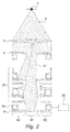
- FIG. 1 shows a simplified schematic drawing of an embodiment of a charged particle lithography apparatus 1.
- lithography systems are described for example in U.S. Patent Nos. 6,897,458 and 6,958,804 and 7,019,908 and 7,084,414 and 7,129,502 , U.S. patent application publication no. 2007/0064213 , and co-pending U.S. patent applications Serial Nos. 61/031,573 and 61/031,594 and 61/045,243 and 61/055,839 and 61/058,596 and 61/101,682 , which are all assigned to the owner of the present invention.
- the lithography apparatus 1 comprises a beamlet generator 2 for generating a plurality of beamlets, a beamlet modulator 8 for patterning the beamlets to form modulated beamlets, and a beamlet projector for projecting the modulated beamlets onto a surface of a target 13.
- the beamlet generator 2 typically comprises a source 3 for producing a charged particle beam 4.
- the source 3 produces a substantially homogeneous, expanding charged particle beam 4.
- source 3 may be referred to as electron source 3 and beam 4 may be referred to as electron beam 4. It must be understood that a similar system as depicted in FIG. 1 may be used with a different type of radiation, for example by using an ion source for producing an ion beam.
- the beamlet generator 2 further comprises a collimator lens 5 for collimating the electron beam 4 produced by the electron source 3, and an aperture array 6 for forming a plurality of beamlets 7.
- the collimator lens 5 may be any type of collimating optical system.
- the electron beam 4 may pass a double octopole (not shown).
- the aperture array 6 comprises a plate provided with a plurality of through holes. The aperture array 6 blocks part of the electron beam 4, whereas a portion of the electron beam 4 passes the aperture array 6 through the holes so as to produce the plurality of electron beamlets 7.
- the system generates a large number of beamlets 122, preferably about 10,000 to 1,000,000 beamlets.
- the beamlet modulator or modulation system 8 in the embodiment of FIG. 1 comprises a beamlet blanker array 9 and a beamlet stop array 10.
- the beamlet blanker array 9 comprises a plurality of blankers for deflecting one or more of the electron beamlets 7.
- the deflected and undeflected electron beamlets 7 arrive at beam stop array 10, which has a plurality of apertures.
- the beamlet blanker array 9 and beam stop array 10 operate together to block or let pass the beamlets 7. Generally, if beamlet blanker array 9 deflects a beamlet 7, it will not pass through the corresponding aperture in beam stop array 10, but instead will be blocked. However, if beamlet blanker array 9 does not deflect a beamlet 7, then it will pass through the corresponding aperture in beam stop array 10.
- beamlets 7 may pass the beamlet stop array 10 upon deflection by corresponding blankers in the beamlet blanker array 9 and be blocked by the beamlet stop array 10 if they are not deflected.
- the lithography system 1 may further comprise a condenser lens array 20.
- the beamlet modulator 8 is arranged to provide a pattern to the beamlets 7 on the basis of pattern data input provided by a control unit 60.
- the control unit 60 comprises a data storage unit 61, a read out unit 62 and a data conversion unit 63.
- the control unit 60 may be located remotely from the rest of the system, for example outside the clean room.
- the pattern data may be transferred via optical fibers 64.
- the light transmitting ends of the optical fibers 64 may be assembled in one or more fiber arrays 15.
- the pattern data carrying light beams 14 are then projected onto corresponding light receiving elements, such as photodiodes, provided on the beamlet blanker array 9. Such projection may be done directly, or via projection system, in FIG. 1 schematically represented by projection lenses 65.
- One or more elements in such projections system may be moveable under control of the control unit 60 via a positioning device 17 to enable proper alignment and/or focusing of the data carrying light beams 14 onto the corresponding light sensitive elements in the beamlet blanker array 9.
- the light sensitive elements are coupled to one or more blankers and are arranged to convert the light signal into a different type of signal, for example an electric signal.
- a pattern data carrying light beam 14 may carry data for one or more blankers within the beamlet blanker array 9. The pattern data is thus sent via the pattern data carrying light beams towards the blankers to enable the blankers to modulate the charged particle beamlets 7 passing there through in accordance with a pattern.
- the modulated beamlets coming out of the beamlet modulator 8 are projected onto a target surface of a target 13 by the beamlet projector.
- the beamlet projector comprises a beamlet deflector array 11 for scanning the modulated beamlets over the target surface and a projection lens arrangement 12 comprising one or more arrays of projection lenses for focusing the modulated beamlets onto the target surface.
- the target 13 is generally positioned on a moveable stage 24, which movement may be controlled by a control unit such as control unit 60.
- the target usually comprises a wafer provided with a charged-particle sensitive layer or resist layer.
- Portions of the resist film will be chemically modified by irradiation of the beamlets of charged particles, i.e. electrons.
- the irradiated portion of the film will be more or less soluble in a developer, resulting in a resist pattern on a wafer.
- the resist pattern on the wafer can subsequently be transferred to an underlying layer, i.e. by implementation, etching and/or deposition steps as known in the art of semiconductor manufacturing.
- the irradiation is not uniform, the resist may not be developed in a uniform manner, leading to mistakes in the pattern.
- High-quality projection is therefore relevant to obtain a lithography system that provides a reproducible result.
- the deflector array 11 and the projection lens arrangement 12 may be integrated into a single end module.
- Such end module is preferably constructed as an insertable, replaceable unit.
- the insertable, replaceable unit may also include the beamlet stop array 10.
- the deflector array 11 may take the form of a scanning deflector array arranged to deflect each beamlet 7 that passes through the beamlet stop array 10.
- the deflector array 11 may comprise a plurality of electrostatic deflectors enabling the application of relatively small driving voltages. Although the deflector array 11 is drawn upstream of the projection lens arrangement 12, the deflector array 11 may also be positioned between the projection lens arrangement 12 and the target surface 13.
- the projection lens arrangement 12 may thus be arranged to focus the beamlets 7 before or after deflection by the deflector array 11.
- the focusing results a geometric spot size of about 10 to 30 nanometers in diameter.
- the projection lens arrangement 12 is preferably arranged to provide a demagnification of about 100 to 500 times, most preferably as large as possible, e.g. in the range 300 to 500 times.
- the projection lens arrangement 12 may be advantageously located close to the target surface 13.
- the charged particle lithography apparatus 1 operates in a vacuum environment.
- a vacuum is desired to remove particles which may be ionized by the charged particle beams and become attracted to the source, may dissociate and be deposited onto the machine components, and may disperse the charged particle beams.
- a vacuum of at least 10 -6 bar is typically required.
- all of the major elements of the lithography apparatus 1 are housed in a common vacuum chamber, including the beamlet generator 2 including the charged particle source 3, the beamlet modulator 8, the beamlet projector system, and the moveable stage 24. These major elements are also referred to as the electron-optical column, or simply as the column, and is schematically represented by the dashed box 18 in FIG. 1 .
- the charged particle source environment is differentially pumped to a considerably higher vacuum of up to 10 -10 mbar.
- the source 3 may be located in a separate chamber, i.e. a source chamber.
- Pumping down the pressure level in the source chamber may be performed in the following way. First, the vacuum chamber and the source chamber are pumped down to the level of the vacuum chamber. Then the source chamber is additionally pumped to a desired lower pressure, preferably by means of a chemical getter in a manner known by a skilled person.
- a chemical getter By using a regenerative, chemical and so-called passive pump like a getter, the pressure level within the source chamber can be brought to a lower level than the pressure level in the vacuum chamber without the need of a vacuum turbo pump for this purpose.
- the use of a getter avoids the interior or immediate outside vicinity of the vacuum chamber being submitted to acoustical and/or mechanical vibrations as would be the case if a vacuum turbo pump or similar would be used for such a purpose.
- FIG. 2 shows a simplified diagram of an electron optical column according to an embodiment of the invention.
- a group of beamlets is depicted as a single beam 27.
- the group of beamlets 27 passes through an aperture array 6 and subsequently through one or more condenser lens arrays 20 until the group 27 arrives at a beamlet blanker array 9.
- the beamlet blanker array 9 may comprise an aperture array, which then forms an integral part of the blanker array 9.
- such aperture array may be a separate array being positioned upstream the blanker array 9.
- the use of an additional aperture array upstream of the blanker array 9 reduces the heat load of the blanker array 9.
- the beamlet blanker array 9 is divided into beam areas 91 and non-beam areas 92.
- the beam areas 91 are areas provided with apertures and are arranged to receive and modulate beamlets passing through these apertures.
- the non-beam areas 92 are areas which are not exposed to charged particle beamlets. These non-beam areas 92 are arranged to provide an area for components needed to support the components within the beam areas 91.
- the non-beam areas 92 may accommodate light sensitive elements, such as photodiodes, for receiving data pattern carrying or modulated light signals, and electrical connections via which the light signals may be forwarded to modulators within the beam areas 91.
- components such as photodiodes and electrical circuits in the non-beam areas are placed at a surface side of the blanker array 9 facing away from the source 3, hereafter referred to as the target side of the blanker array 9.
- a cooling arrangement 93 is provided on the surface side of the blanker array 9 facing the source 3, hereafter the source side of the blanker array 9, .
- the cooling arrangement 93 comprises one or more cooling channels for accommodating a flow of a cooling fluid, such as water. and water flowing in the channels can be placed on an upper surface of non-beam areas 92.
- the cooling arrangement 93 is located within the non-beam areas 92 of the blanker array 9 to avoid that any components thereof may block or directly interact with charged particles from the group of beamlets 27.
- the cooling arrangement 93 may be coupled to a coolant system 25 for providing cooling fluid to the inlet of the cooling arrangement at a suitable speed.
- a coolant system 25 for providing cooling fluid to the inlet of the cooling arrangement at a suitable speed.
- such flow speed should be sufficiently high to produce a turbulent flow of cooling fluid through the plurality of cooling channels.
- the coolant system may be arranged to provide the cooling fluid with a sufficiently low flow speed to produce a laminar flow of cooling fluid through the plurality of cooling channels.
- the cooling arrangement 93 may also include measures to create a certain type of flow, e.g. a turbulent flow or a laminar flow.
- embodiments of the invention will be discussed in which a cooling arrangement is disposed on top of a beamlet blanker array 9. Additionally, with reference to FIGS. 9 and 10 , embodiments of the invention will be discussed in which a cooling arrangement is disposed on top of a beamlet stop array. However, it must be understood, as will be apparent from the column shown in FIG. 2 , that such cooling arrangement may be provided on surface of other components within the electron optical column. In particular, embodiments of the cooling arrangement may be used on a surface of a plate provided with a plurality of apertures for letting the beamlets pass through the plate.
- Such plates include but are not limited to an aperture array such as aperture array 6, a lens plate such as a plate that is part of the one or more condenser lens arrays 20 or a plate that is part of the projector lens arrangement 12 shown in FIG. 1 , and a plate in a beamlet modulator 8, such as beamlet blanker array 9 and/or beamlet stop array 10.
- the apertures do not need to be current limiting apertures.
- heat may be generated by other means than impingement of charged particles within the charged particle beamlets.
- the beamlet blanker array 9 comprises electronic circuitry that generates heat.
- charged particles may scatter upon components resulting in secondary charged particles which may transfer energy to other components as well.
- the cooling fluid preferably comprises water.
- Water is easier to use than other known cooling fluids, such as ammonia.
- Ammonia requires a high pressure system and more extensive safety measures.
- a liquid metal such as liquid gallium, could also be used, however water has a much larger allowable flow speed range than gallium, and the use of gallium introduces other complications such as solidification, cost, corrosivity, and diffusion.
- a suitable temperature at the inlet 31 appears to be 15-25 °C, preferably about 20 °C.
- FIG. 3 shows a schematic cross-sectional view of a portion of a beamlet blanker array 9 provided with a cooling channel 94 that is part of the cooling arrangement 93.
- the cooling channel 94 is arranged to accommodate a flow of a cooling fluid 96.
- the flow is a forced flow by an external source, i.e. coolant system 25 in FIG. 2 , to obtain forced convection in the cooling channel 94.
- the cooling arrangement 93 is connected to the beamlet blanker array 9 by means of an adhesive layer 97.
- the adhesive being used in the adhesive layer 97 has a sufficiently high thermal conductivity to provide as much cooling capacity as possible.
- the adhesive layer has a heat transfer coefficient greater than 100 kW/m 2 ⁇ K, more preferably greater than 150 kW/ m 2 ⁇ K.
- Heat transfer via the cooling fluid within the cooling arrangement 93 improves the role of the arrangement 93 in removing heat away from the beamlet blanker array 9 so as to keep the beamlet blanker array 9 below a threshold temperature.
- the extent of heat transfer between a side wall 95 of the cooling channel 94 and the cooling fluid 96 can be indicated by a heat transfer coefficient. Experiments have shown that the heat transfer coefficient generally increases with the flow speed of cooling fluid 96 in the channel.
- Another advantage of a relatively high flow speed of cooling fluid 96 in the channel 94 is that such speed reduces the temperature difference ⁇ T between the temperature of the cooling fluid at entry of the channel 94 and the temperature of the cooling fluid at the exit of the channel 94. As a result, the heat absorbing capacity of the cooling fluid does not change significantly as a function of channel position, and cooling can be effected in a more homogeneous way.
- the flow speed may be such that the fluid flow is a laminar flow.
- the use of a laminar flow reduces the generation of vibrations caused by interaction between the cooling fluid 96 and the cooling arrangement 93.
- the corrosion erosion is much lower for a laminar flow than for a turbulent flow.
- a turbulent flow is more preferable than a laminar flow.
- a truly laminar flow there is no flow component perpendicular to the channels walls, so any heat transfer in that direction occurs solely via much less efficient conduction in the cooling fluid.
- heat will be transferred in a direction perpendicular to the channel walls. Consequently, the cooling fluid can absorb more heat.
- convection is the ideal mechanism to transfer heat away from the optical component in an effective way. Although conductive heat transfer will always occur to some extent, convective heat transfer is generally dominant.
- the cooling arrangement 93 is preferably made of a material that has a coefficient of thermal expansion (CTE) that is similar, or at least not too different, from the CTE of the beamlet blanker array material. A too large difference in CTE between the cooling arrangement material and the beamlet blanker array material may cause deformation of the beamlet blanker array.
- the adhesive layer preferably has a CTE that is not too different as well to ensure that the cooling arrangement 93 and the beamlet blanker array 9 remain at substantially the same position with respect to each other in case the beamlet blanker array expands due to exposure to heat originating from impingement of charged particles on its source surface side. Furthermore, the beamlet blanker array 9 may expand as a result of heat used in circuitry within the non-beam areas. Table 1 CTE of different materials Material CTE [ ⁇ m/m ⁇ K] Silicon 2.6 Tungsten / AlN 4.5 Titanium 8.6 Copper 16.5
- the beamlet blanker array material will be silicon.
- silicon has a CTE of 2.6 ⁇ m/m ⁇ K.
- Typical materials for a cooling arrangement 93 would be copper (Cu), tungsten (W), aluminum nitride (AlN) and titanium (Ti).
- copper is the least suitable to be used for a cooling arrangement that is provided on a silicon beamlet blanker array, because the CTE of copper is by far the highest, i.e. 16.5 ⁇ m/m ⁇ K. ⁇
- FIG. 4A shows an elevated cross-sectional top view of the cooling arrangement 93 without cooling fluid flowing there through.
- the cooling channels 94 in the cooling arrangement 93 are generally closed cooling channels, i.e. channels entirely surrounded by side walls along their length.
- a cover for covering the different components of the cooling arrangement for example to serve as a side wall for cooling channels 94, is not shown for clarity reasons. Such cover prevents that cooling fluid can leak out of the cooling arrangement 93.
- the cooling arrangement 93 comprises a flat surface 37 for connecting to the plate with apertures to allow the flat surface 37 to function as a heat transfer surface.
- the cooling arrangement 93 is provided on the surface side 37 with two cut-out volumes in accordance with the lay-out of the cooling channels 94.
- the perimeters for the cut-out volumes define cut-out apertures 38.
- the cooling arrangement 93 is provided with one or more inlets 31 for receipt of cooling fluid and one or more outlets 35 for removal of cooling fluid.
- the cooling fluid flows from the one or more inlets 31 towards the one or more outlets 35 through a cooling channels 94 while capturing heat along the way.
- the number of cooling channels 94 exceeds the number of inlets 31 and outlets 35. Further details with respect to this design will be discussed with reference to FIGS. 5 and 6 .
- the cooling arrangement 93 is provided with slots 34 that are positioned over beam areas of the beamlet blanker array 9.
- the cooling arrangement may cover and be in contact with the blanker array over most, preferably all, surface area reserved for the non-beam areas.
- FIG. 4B is a cross-sectional view of the cooling arrangement 93 depicted in FIG. 4A along the line IVb - IVb'.
- the cooling arrangement 93 does not occupy too much space.
- the cooling arrangement 93 should not interfere with the optimal position of other components within the electron optical column. That is, in many cases the height of the cooling arrangement is restricted so to avoid that an adjacent component in the electron optical column, i.e. a component upstream if the cooling arrangement is arranged at the source side of the blanker array 9 or a component downstream if the cooling arrangement is arranged at the target side of the blanker array 9, can not be positioned at its desired position.
- electron optical components in the electron optical column are generally placed in such a way that their influence on the charged particle beamlets is optimal for the electron optical performance of the column.
- the dimensions of the cooling arrangement 93 are limited by the presence of the condenser lens array 20.
- the height d 1 of the cooling channels 94 on top of the beamlet blanker array 9 is limited in view of abovementioned reason.
- the height d 2 of cooling channel or reservoir 36 connected to the inlet 31 may be higher.
- a similar height d 2 may be used in a cooling channel or reservoir connected to the outlet 35.
- the use of a greater height d 2 at locations where such space is available has the advantage that a sufficient amount of cooling fluid can be provided and/or removed.
- the presence of multiple cooling channels of limited height ensures that the beamlet blanker array can be sufficiently cooled.
- Exemplary dimensions for heights d 1 and d 2 are 1-3 mm, e.g. 1.7 mm, and 3-10 mm, e.g. 4.0 mm, respectively.
- FIG. 5 shows a portion of the cooling fluid channel lay-out according to an embodiment of the invention.
- the inlet 31 is connected to the plurality of cooling channels 94 via a single distribution channel or tube.
- the single distribution channel comprises a diffuser section 41 for diffusing cooling fluid and a splitting section 42 for dividing the cooling fluid over the plurality of cooling channels 94. Dividing the cooling fluid flow over multiple channels 94 allows to spread resistance caused by a turbulent fluid flow.
- FIG. 6 shows a top view of the cooling fluid channel lay-out of FIG. 5 .
- the height of the cooling channel lay-out is higher at a position close to the inlet 31 than at a position close to the plurality of cooling channels 94.
- the space available for the cooling channels 94 may be limited.
- the fluid is preferably supplied at a velocity sufficiently high to create a turbulent flow through the cooling channels 94, for example by using a coolant system 25 as depicted in FIG. 2 .
- the cooling arrangement 93 is thicker at locations further away from beam areas, and the inlet 31 is then located in such thicker portion.
- the inlet 31 may then have a relatively large cross-sectional area.
- the diffuser section allows the fluid to diffuse in such a way that the flow can be spread as homogeneously as possible over the plurality of cooling channels within the splitting section 42.
- the cross-sectional area of the flow path at entry of the diffuser section is preferably the same as the cross-sectional area of the flow path at the exit of the diffuser section exit.
- Such dimensioning ensures that the cooling fluid enters and exits the diffuser section 41 at substantially the same velocity. In FIG. 6 , the dimensions may thus be such that for a rectangular cross-section d I times the height at entry equals d II times the height at the exit of the diffuser section.
- the cross-sectional areas of the one or more channels being substantially aligned with the inlet have smaller dimensions than the cross-sectional areas of channels that are more offset with respect to the inlet.
- the center channel has a diameter d M that is smaller than the diameter d S of the side channels.
- the use of different cross-sectional areas may help to evenly spread fluid resistance over the multiple channels 94.
- the cooling arrangement 93 is manufactured by assembling multiple bodies onto each other.
- the size and shape of the bodies may depend on the materials being used, the method of assembly and the dimensions at hand.
- FIGS. 7A, 7B schematically show cross-sectional views of a portion of the cooling arrangement 93, in this case a channel 94 prior to assembly.
- the cooling arrangement 93 of FIG. 7A is manufactured by assembling two bodies 93a, 93b onto each other. Both bodies 93a, 93b are shaped such that a significant portion of a channel is formed therein, in this case the cut-out area in each body 93a, 93b contributes for about 50% to the channel(s) being formed.
- the two bodies 93a, 93b are connected to each other with an adhesive in areas 51. Such assembly is effective if the bodies 93a, 93b are made of AlN.
- the cooling arrangement 93 of FIG. 7B is also manufactured by assembling two bodies 93a, 93b.
- the first body 93a contributes primarily to the channel, while the second body 93b only serves to close the channel.
- the second body 93b may be connected to the first body 93a by laser welding in area 52.
- the area 52 is bounded by the edge of the cut-out aperture 38.
- Such assembly may be used if titanium is used as the cooling arrangement material.
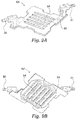
- FIGS. 8A, 8B show an elevated bottom and top view of a cooling arrangement 93 according to an embodiment of the invention.
- the cooling arrangement has been made in accordance with the assembly technique shown in FIG. 7B .
- This embodiment of the cooling arrangement 93 which is similar to the embodiment described with reference to FIG.4A , is formed by a flat body provided with six cooling channels 94 that are separated by five slots 34. These slots 34 are configured to be positioned over beam areas of the plate provided with apertures (e.g. the beamlet blanker array 9 or the beamlet stop array 10 of the lithography system) in such a manner that interference by the cooling arrangement 93 with charged particle beamlets is avoided.
- the cooling arrangement 93 may cover and be in contact with the plate over most, preferably all, surface area that is reserved for the non-beam areas.
- the cooling arrangement 93 in FIGS.8A and 8B may be manufactured by joining a first body 93a with two second bodies 93b.
- the first body is formed as a plate-shaped body 93a provided with the six cooling channels 94 and the five slots 34.
- the plate-shaped body 93a is preferably made from titanium.
- the plate-shaped body 93a comprises a flat surface 37 that spans a contact plane P for connecting to the plate with apertures, so as to allow the flat surface 37 to function as a heat transfer surface.
- the six cooling channels 94 are arranged coplanar and (substantially) mutually parallel to define a flow direction F.
- the plane spanned by the six cooling channels 94 is substantially parallel with the flat surface side 37 and thus with the contact plane P.
- Each cooling channel 94 is along at least one side thereof (as viewed in the flow direction F) bounded by one slot 34.
- Each slot 34 has an elongate shape along the flow direction F i.e. parallel with the cooling channels 94.
- the cooling arrangement 93 in FIGS.8A and 8B is provided with two inlets 31 for receiving cooling fluid into the cooling arrangement 93, and two outlets 35 for discharging cooling fluid from the cooling arrangement 93. During cooling operation, the cooling fluid flows from the two inlets 31 towards the two outlets 35 through the cooling channels 94, while extracting thermal energy from the plate with apertures along the way.
- the cooling arrangement 93 is thicker at outer regions 39 of the plate shaped body 93a, this thickness corresponding to a direction perpendicular to the contact plane P.
- the inlets 31 and the outlets 35 are located in the thicker outer regions 39, and allow the inlets 31 and the outlets 35 to have cross-sectional areas that are larger than the cross-sectional areas of the cooling channels 94.
- the inlets 31 and outlets 35 also run substantially parallel to the flow direction F, thereby minimizing any obstruction of the fluid flow.
- One inlet 31 is connected to three cooling channels 94 via a single distribution channel, which comprises a diffuser section 41 and a splitting section 42 as was described with reference to FIGS.5 and 6 .
- the outlet 35 is similarly provided with a three-way distribution channel.
- the distribution channel of each of the two inlets 31 splits up into three cooling channels 94, and these three cooling channels 94 subsequently merge back into the distribution channel of one of the two outlets 35.
- the plate-shaped body 93a with the two inlets 31 and the two outlets 35 is provided entirely on one side of the contact plane P (i.e. in the first half space).
- the flat surface side 37 can be attached at the other side of the contact plane P (i.e. in the other half space) as a heat transfer surface to any desired portion of the plate with apertures in the lithography system (e.g. the beamlet blanker array 9 or the beamlet stop array 10), without obstruction by any other portion of the cooling arrangement 93.
- the plate-shaped body may be obtained by providing the first body 93a on the surface side 37 with two cut-out volumes in accordance with the lay-out of the cooling channels 94.
- a perimeter of each cut-out volume near the surface side 37 defines a cut-out aperture 38 (see FIG.4A ).
- the resulting two cut-out apertures 38 are covered by the second bodies 93b, which are formed by cover plates that each has a shape which is similar to the cut-out apertures 38, and which is arranged to cover the cut-out volume flush with the flat surface side 37.
- the two cover plates 93b are positioned over the two cut-out apertures 38, so as to form the cooling channels 94 in accordance with the assembly technique illustrated by FIG. 7B .
- the cooling channels 94 may thus be formed to define a channel lay-out with rectangular cross-sections (viewed perpendicular to the flow direction F).
- the described assembly technique is particularly suitable for manufacturing this rectangular channel layout.
- the cover plates 93b may be connected to the first body 93a by laser welding the respective cover plate 93b along the contour of the corresponding cut-out aperture 38.
- the cover plates 93b are preferably also made from titanium. The technique of providing the cut-out volumes in the plate shaped body 93a and covering the cut-out volumes with the cover plates 93b on the flat surface side 37 yields an optimal balance between good heat transfer properties on the one hand and good manufacturing accuracy on the other hand.
- Typical lengths for the cooling channels 94 and the slots 34 may for example be in the range of 25 millimeters to 50 millimeters, preferably 37 millimeters.
- Typical external widths of the cooling channels 94 may be 3 millimeters to 4 millimeters, preferably 3.5 millimeters, and typical internal widths of the cooling channels 94 may be 2 millimeters to 3 millimeters, preferably 2.5 millimeters.
- Typical widths of the slots 34 may be 2 millimeters to 3 millimeters, preferably 2.5 millimeters.
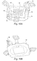
- FIGS. 9A, 9B show an elevated top and bottom view of another cooling arrangement 93' according to an embodiment of the invention.
- the cooling arrangement 93' also includes a plurality of cooling channels 94 connecting an inlet 31 with an outlet 35.
- the cooling channels 94 in the cooling arrangement 93' have an open structure, as is shown in FIG. 9B .
- the cooling arrangement 93' comprises a distribution channel 43 connecting the inlet 31 with the plurality of cooling channels 94, the distribution channel 43 being arranged for receiving the cooling fluid 31 from the inlet 31, for example supplied via a coolant system 25, and guiding the cooling fluid in such a way that the cooling fluid is transferred through the cooling channels 94 in a laminar flow regime.
- the cooling fluid may have a negligible influence on the structure to be cooled with respect to vibrations.
- the inlet 31 and the outlet 35 are preferably placed diagonally with respect to the orientation of the cooling channels 94 between the beam areas to reduce cooling inhomogeneity as a function of location caused by a somewhat higher temperature difference between the cooling fluid at cooling channel entry and the cooling fluid at cooling channel exit as compared to such temperature difference in case of a high-speed, turbulent flow.
- FIGS. 10A, 10B show an elevated top and bottom of the cooling arrangement 93' of FIGS. 9A, 9B disposed on a beamlet stop array 10.
- the cooling channels 94 are closed, and leakage of cooling fluid out of the combination of the cooling arrangement 93' and the beamlet stop array 10 may be avoided.
- the cooling arrangement 93' may in particular also be useful to cool vibrationally sensitive components within a lithography system, for example a critical lens plate of a projection lens array in a beamlet projector.
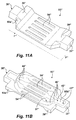
- FIGS. 11A and 11B show an elevated bottom and top view of another cooling arrangement 93" according to embodiment of the invention.
- the cooling arrangement 93" represents an alternative to the embodiment described with reference to FIGS.8A and 8B , and a majority of features in the cooling arrangement 93 described there may also be present in the cooling arrangement 93" shown in FIGS.11A and 11B . These features will not be discussed here again. For the features that are discussed here, similar reference numbers are used for similar features, but indicated by primes to distinguish the embodiments.
- the cooling arrangement 93" is again formed by a flat body provided with six cooling channels 94" that are separated by five slots 34" configured for positioning over plate beam areas.
- the cooling arrangement 93" is provided with a single inlet 31" for receiving of cooling fluid, and a single outlet 35" for discharging the cooling fluid.
- the cooling fluid flows from the inlet 31" towards the outlet 35" through the six cooling channels 94" along flow direction F".
- the cooling fluid flowing through the cooling channels 94" may collect thermal energy along the way that may for example originate from a hot planar object that is connected to the flat surface side 37" along the contact plane P".
- the cooling arrangement 93" is thicker at outer regions 39" of the plate-shaped body 93a", and the inlet 31" and the outlet 35" are located in these thicker outer regions 39".
- the inlet 31" is connected to the six cooling channels 94" via a two-staged distribution channel.
- the two-staged distribution channel of the inlet 31" comprises a diffuser section (41") for diffusing cooling fluid, and a splitting section (42") for dividing the cooling fluid over the cooling channels 94", these sections being similar to the ones in the distribution channel as described herein above with reference to FIGS.5 and 6 .
- the inlet channel 31" initially branches off into three channels that each comprises a divergent section 40". These divergent sections 40" preferably diverge (i.e.
- each channel subsequently splits up into two adjacent cooling channels 94" that are laterally separated by a slot 34". At the other end of the slots 34" (viewed along the flow direction F"), each of the adjacent pairs of cooling channels 94" subsequently merges back into a further channel.
- Each of the three further channels comprises a convergent section 44", which is preferably formed by a smooth lateral narrowing of the channel.
- the three further channels join into the outlet channel 35" by means of a two-staged distribution channel complementary to the one provided at the inlet 31".
- the plate-shaped body 93a" may be obtained by providing a single cut-out volume in accordance with a lay-out of the six cooling channels 94" on the flat surface side 37", and may also be manufactured in accordance with the technique illustrated by FIG.7B .
- a perimeter of the cut-out volume near the surface side 37" defines a single cut-out aperture.
- the resulting cut-out aperture is covered by a cover plate 93b" that has a shape matching the contour of the cut-out aperture, in such a manner that the cover plate 93b" can be positioned flush with the flat surface side 37".
- This cooling channel 94" lay-out requires only a single cut-out volume, and allows connection to single conduits for the supply and discharge of cooling fluid.
- the inlet 31" and the outlet 35" each have a cross-sectional area that equals the sum of the cross-sectional areas of the cooling channels 94".
Landscapes
- Engineering & Computer Science (AREA)
- Chemical & Material Sciences (AREA)
- Nanotechnology (AREA)
- Crystallography & Structural Chemistry (AREA)
- Physics & Mathematics (AREA)
- Analytical Chemistry (AREA)
- Mathematical Physics (AREA)
- Theoretical Computer Science (AREA)
- Condensed Matter Physics & Semiconductors (AREA)
- General Physics & Mathematics (AREA)
- Manufacturing & Machinery (AREA)
- Electron Beam Exposure (AREA)
- Exposure And Positioning Against Photoresist Photosensitive Materials (AREA)
Claims (15)
- Lithographiesystem (1) mit mehreren Beamlets geladener Teilchen zum Belichten eines Ziels (13) unter Verwendung von Beamlets (7) geladener Teilchen, wobei das System- einen Beamletgenerator (2) zur Erzeugung der Beamlets geladener Teilchen;- einen Beamletmodulator (8) zum Mustern der Beamlets, um modulierte Beamlets zu bilden;- einen Beamletprojektor (12) zum Projizieren der modulierten Beamlets auf eine Fläche des Zielsumfasst;
wobei der Beamletgenerator, der Beamletmodulator und/oder der Beamletprojektor eine oder mehrere Platten umfasst, die mit mehreren Öffnungen versehen ist bzw. sind, um die Beamlets durch die Platte verlaufen zu lassen, wobei die Öffnungen in Gruppen angeordnet sind, um an der Fläche der einen oder der mehreren Platten mehrere Strahlbereiche (91) zu bilden, die von mehreren Nichtstrahlbereichen (92), welche keine Öffnungen für den Durchgang der Beamlets enthalten, abgegrenzt und getrennt sind; und
wobei wenigstens eine der Platten mit Öffnungen in dem Lithographiesystem mit einer Kühlanordnung (93) versehen ist, die in einem oder mehreren Nichtstrahlbereichen an ihrer Fläche angeordnet ist, wobei die Kühlanordnung einen plattenförmigen Körper umfasst, der mit einem Einlass (31) zum Erhalt einer Kühlflüssigkeit, mehreren Kühlkanälen (94), die für den Fluss einer Kühlflüssigkeit in ihrem Inneren bereitgestellt sind, und einem Auslass (35) zur Beseitigung der Kühlflüssigkeit versehen ist, wobei der plattenförmige Körper mit mehreren Schlitzen (34) zwischen den Kühlkanälen versehen ist, und wobei die Schlitze im Wesentlichen mit den Strahlbereichen an der Öffnungsplattenfläche ausgerichtet sind; und dadurch gekennzeichnet, dass
der Einlass und die mehreren Kühlkanäle miteinander über einen einzelnen Verteilungskanal verbunden sind, wobei der einzelne Verteilungskanal einen Diffusorabschnitt (41) zum Diffundieren von Kühlflüssigkeit und einen Aufteilabschnitt (42) zum Verteilen der Kühlflüssigkeit über die mehreren Kühlkanäle (94) umfasst. - System nach Anspruch 1, wobei der Diffusorabschnitt an einer Seite, die zu dem Einlass (31) gewandt ist, eine erste Querschnittfläche aufweist, und zu den mehreren Kühlkanälen gewandt eine zweite Querschnittfläche aufweist;
wobei die erste Querschnittfläche und die zweite Querschnittfläche gleich sind; und
wobei die Höhe der ersten Querschnittfläche größer als die Höhe der zweiten Querschnittfläche ist, wobei die Höhe in einer Richtung verläuft, die sich senkrecht zu einem flachen Abschnitt des plattenförmigen Körpers, durch den die Kühlkanäle verlaufen, erstreckt. - System nach Anspruch 1 oder 2, wobei der plattenförmige Körper eine flache Fläche (37) umfasst, die eine Kontaktebene (P) zur Verbindung mit der Platte, die mit Öffnungen versehen ist, überspannt,
wobei die Kühlkanäle (94) untereinander im Wesentlichen parallel angeordnet sind, um eine Fließrichtung (F) zu definieren, die im Wesentlichen parallel zu der Kontaktebene (P) verläuft. - System nach einem der vorhergehenden Ansprüche, wobei der plattenförmige Körper der Kühlanordnung durch eine Klebstoffschicht (97) mit der wenigstens einen Platte, die mit Öffnungen versehen ist, verbunden ist, wobei die Klebstoffschicht (97) vorzugsweise einen gesamten Wärmeübergangskoeffizienten von mehr als 100 kW/m2□K und vorzugsweise mehr als 150 kW/m2□K aufweist.
- System nach einem der vorhergehenden Ansprüche, ferner umfassend ein Kühlmittelsystem (25), das eingerichtet ist, um dem Einlass der Kühlanordnung eine Kühlflüssigkeit mit einer ausreichend hohen Fließgeschwindigkeit bereitzustellen, um eine Wirbelströmung der Kühlflüssigkeit durch die mehreren Kühlkanäle zu erzeugen.
- System nach einem der vorhergehenden Ansprüche, wobei der Beamletmodulator eine Beamletaustastanordnung (9) und eine Beamletanhalteanordnung (10) umfasst, und wobei der plattenförmige Körper der Kühlanordnung an einer Fläche der Beamletaustastanordnung angeordnet ist.
- System nach einem der Ansprüche 1 bis 4, ferner umfassend ein Kühlmittelsystem (25), um dem Einlass der Kühlanordnung eine Kühlflüssigkeit mit einer ausreichend geringen Fließgeschwindigkeit bereitzustellen, um eine laminare Strömung der Kühlflüssigkeit durch die mehreren Kühlkanäle zu erzeugen, wobei vorzugsweise der Beamletmodulator eine Beamletaustastanordnung (9) und eine Beamletanhalteanordnung (10) umfasst, und wobei der plattenförmige Körper der Kühlanordnung an einer Fläche der Beamletanhalteanordnung angeordnet ist.
- System nach Anspruch 7, wobei der plattenförmige Körper der Kühlanordnung an einer Fläche einer Öffnungsplatte des Beamletprojektors angeordnet ist.
- System nach einem der vorhergehenden Ansprüche, wobei die Kühlflüssigkeit Wasser umfasst.
- System nach einem der vorhergehenden Ansprüche, wobei der plattenförmige Körper der Kühlanordnung aus Titan besteht.
- Verfahren zur Herstellung eines Kühlkörpers zur Verwendung an der Oberseite einer mit mehreren Öffnungen versehenen Fläche einer Platte zur Verwendung in einem Lithographiesystem mit mehreren Beamlets geladener Teilchen, wobei die Öffnungen in Gruppen angeordnet sind, um an der Fläche der Platte mehrere Strahlbereiche (91) zu bilden, wobei das Verfahren umfasst:- Bereitstellen eines plattenförmigen Körpers, wobei eine Flächenseite (37) des Körpers mit einem ausgeschnittenen Volumen gemäß einer Anordnung versehen ist;- Bereitstellen mehrerer Schlitze (34) in dem plattenförmigen Körper, wobei die Schlitze so angeordnet sind, dass sie mit den Strahlbereichen an der Öffnungsplattenfläche ausgerichtet sind;- derartiges Abdecken des ausgeschnittenen Volumens, dass in dem Körper mehrere Kühlkanäle (94) gebildet werden, wobei die Schlitze (34) zwischen den Kühlkanälen (94) angeordnet sind, wobei die mehreren Kühlkanäle einen Einlass an einer Seite des Körpers mit einem Auslass an einer anderen Seite des Körpers verbinden.
- Verfahren nach Anspruch 11, wobei das Abdecken ein Verbinden einer oder mehrerer Abdeckplatten durch Laserschweißen mit dem Körper umfasst.
- Verfahren nach Anspruch 11 oder 12, wobei der Körper aus Titan besteht.
- Verfahren nach Anspruch 11, wobei das Abdecken ein Kleben der Öffnungsplatte, die gekühlt werden soll, an den Körper umfasst.
- Verfahren zur Herstellung eines Kühlkörpers zur Verwendung an der Oberseite einer mit mehreren Öffnungen versehenen Fläche einer Platte zur Verwendung in einem Lithographiesystem mit mehreren Beamlets geladener Teilchen, wobei die Öffnungen in Gruppen angeordnet sind, um an der Fläche der Platte mehrere Strahlbereiche (91) zu bilden, wobei das Verfahren umfasst:- Bereitstellen eines ersten plattenförmigen Körpers, wobei eine Flächenseite des ersten Körpers mit einem ersten ausgeschnittenen Volumen gemäß einer ersten Anordnung versehen ist;- Bereitstellen eines zweiten plattenförmigen Körpers, wobei eine Flächenseite des zweiten Körpers mit einem zweiten ausgeschnittenen Volumen gemäß einer zweiten Anordnung versehen ist;- Bereitstellen mehrerer Schlitze (34) in dem ersten und dem zweiten plattenförmigen Körper, wobei die Schlitze so angeordnet sind, dass sie mit den Strahlbereichen an der Öffnungsplattenfläche ausgerichtet sind; und- derartiges Verbinden der Flächen des ersten Körpers und des zweiten Körpers übereinander, dass das erste ausgeschnittene Volumen und das zweite ausgeschnittene Volumen in einem zusammengesetzten Körper mehrere Kühlkanäle bilden, wobei die Schlitze (34) zwischen den Kühlkanälen (94) angeordnet sind, wobei die mehreren Kühlkanäle einen Einlass an einer Seite des zusammengesetzten Körpers mit einem Auslass an einer anderen Seite des zusammengesetzten Körpers verbinden,wobei das Verbinden vorzugsweise durch Bereitstellen einer Klebstoffschicht zwischen den Flächen des ersten Körpers und des zweiten Körpers durchgeführt wird.
Applications Claiming Priority (2)
| Application Number | Priority Date | Filing Date | Title |
|---|---|---|---|
| US201261646398P | 2012-05-14 | 2012-05-14 | |
| PCT/EP2013/059948 WO2013171216A1 (en) | 2012-05-14 | 2013-05-14 | Charged particle multi-beamlet lithography system and cooling arrangement manufacturing method |
Publications (2)
| Publication Number | Publication Date |
|---|---|
| EP2850635A1 EP2850635A1 (de) | 2015-03-25 |
| EP2850635B1 true EP2850635B1 (de) | 2016-04-27 |
Family
ID=48444378
Family Applications (1)
| Application Number | Title | Priority Date | Filing Date |
|---|---|---|---|
| EP13722748.4A Active EP2850635B1 (de) | 2012-05-14 | 2013-05-14 | Ladungsträger-lithografiesystem mit mehreren teilstrahlen und kühlanordnungsherstellungsverfahren |
Country Status (6)
| Country | Link |
|---|---|
| EP (1) | EP2850635B1 (de) |
| JP (1) | JP5973061B2 (de) |
| KR (1) | KR101945964B1 (de) |
| CN (1) | CN104471669B (de) |
| NL (1) | NL2010799C2 (de) |
| WO (1) | WO2013171216A1 (de) |
Families Citing this family (9)
| Publication number | Priority date | Publication date | Assignee | Title |
|---|---|---|---|---|
| JP6219374B2 (ja) | 2012-05-14 | 2017-10-25 | マッパー・リソグラフィー・アイピー・ビー.ブイ. | 荷電粒子リソグラフィシステムおよびビーム発生器 |
| US11348756B2 (en) | 2012-05-14 | 2022-05-31 | Asml Netherlands B.V. | Aberration correction in charged particle system |
| KR102124913B1 (ko) * | 2013-09-07 | 2020-06-22 | 에이에스엠엘 네델란즈 비.브이. | 타겟 프로세싱 유닛 |
| EP3069368B1 (de) * | 2013-11-14 | 2021-01-06 | ASML Netherlands B.V. | Elektrodenkühlanordnung |
| US10486232B2 (en) | 2015-04-21 | 2019-11-26 | Varian Semiconductor Equipment Associates, Inc. | Semiconductor manufacturing device with embedded fluid conduits |
| US9829804B1 (en) | 2016-07-28 | 2017-11-28 | Mapper Lithography Ip B.V. | Substrate holding device, method for manufacturing such a device, and use of such a device in a lithography system |
| CN108121164B (zh) * | 2016-11-29 | 2020-12-01 | 中芯国际集成电路制造(上海)有限公司 | 光罩散热装置及其工作方法 |
| NL1042970B1 (en) * | 2017-08-28 | 2019-06-26 | Asml Netherlands Bv | Memory device with predetermined start-up value |
| US20220276008A1 (en) * | 2021-02-26 | 2022-09-01 | Teradyne, Inc. | Thermal plate having a fluid channel |
Family Cites Families (25)
| Publication number | Priority date | Publication date | Assignee | Title |
|---|---|---|---|---|
| US3157308A (en) | 1961-09-05 | 1964-11-17 | Clark Mfg Co J L | Canister type container and method of making the same |
| US3159408A (en) | 1961-10-05 | 1964-12-01 | Grace W R & Co | Chuck |
| US4524308A (en) | 1984-06-01 | 1985-06-18 | Sony Corporation | Circuits for accomplishing electron beam convergence in color cathode ray tubes |
| WO1994025880A1 (en) | 1993-04-30 | 1994-11-10 | Board Of Regents, The University Of Texas System | Megavoltage scanning imager and method for its use |
| EP0766405A1 (de) | 1995-09-29 | 1997-04-02 | STMicroelectronics S.r.l. | Register mit schrittweiser Annäherung ohne Redundanz |
| US6046457A (en) * | 1998-01-09 | 2000-04-04 | International Business Machines Corporation | Charged particle beam apparatus having anticontamination means |
| JP2000348662A (ja) * | 1999-06-02 | 2000-12-15 | Nikon Corp | 荷電粒子線照射系、荷電粒子線露光装置及び半導体デバイス製造方法 |
| JP4355446B2 (ja) * | 2000-12-28 | 2009-11-04 | 株式会社アドバンテスト | 電子ビーム露光装置及び電子ビーム成形部材 |
| US6563124B2 (en) | 2001-03-21 | 2003-05-13 | Applied Materials, Inc. | Electron beam apparatus having traversing circuit boards |
| US6768125B2 (en) * | 2002-01-17 | 2004-07-27 | Ims Nanofabrication, Gmbh | Maskless particle-beam system for exposing a pattern on a substrate |
| KR101368027B1 (ko) | 2002-10-25 | 2014-02-26 | 마퍼 리쏘그라피 아이피 비.브이. | 리소그라피 장치 |
| KR101119890B1 (ko) | 2002-10-30 | 2012-03-13 | 마퍼 리쏘그라피 아이피 비.브이. | 전자 빔 노출 시스템 |
| EP1602121B1 (de) | 2003-03-10 | 2012-06-27 | Mapper Lithography Ip B.V. | Vorrichtung zur erzeugung einer vielzahl von teilstrahlen |
| JP4113032B2 (ja) * | 2003-04-21 | 2008-07-02 | キヤノン株式会社 | 電子銃及び電子ビーム露光装置 |
| EP1627412B1 (de) | 2003-05-28 | 2007-04-04 | Mapper Lithography Ip B.V. | Beamlet-belichtungssystem mit geladenen teilchen |
| EP1660945B1 (de) | 2003-07-30 | 2007-12-19 | Mapper Lithography Ip B.V. | Modulator-schaltkreise |
| US7145641B2 (en) * | 2003-12-31 | 2006-12-05 | Asml Netherlands, B.V. | Lithographic apparatus, device manufacturing method, and device manufactured thereby |
| JP3929459B2 (ja) * | 2004-11-11 | 2007-06-13 | 株式会社日立ハイテクノロジーズ | 荷電粒子線露光装置 |
| TWI345685B (en) * | 2005-09-06 | 2011-07-21 | Asml Netherlands Bv | Lithographic method |
| US7709815B2 (en) | 2005-09-16 | 2010-05-04 | Mapper Lithography Ip B.V. | Lithography system and projection method |
| EP2638560B1 (de) * | 2010-11-13 | 2017-02-22 | Mapper Lithography IP B.V. | Lithografhiesystem mit geladenen teilchen und aperturanordnungskühlung |
| US8586949B2 (en) * | 2010-11-13 | 2013-11-19 | Mapper Lithography Ip B.V. | Charged particle lithography system with intermediate chamber |
| JP5253532B2 (ja) * | 2011-03-01 | 2013-07-31 | キヤノン株式会社 | 偏向器アレイ、偏向器アレイの製造方法、描画装置、および物品の製造方法 |
| NL2007604C2 (en) * | 2011-10-14 | 2013-05-01 | Mapper Lithography Ip Bv | Charged particle system comprising a manipulator device for manipulation of one or more charged particle beams. |
| EP3279624B1 (de) | 2015-04-03 | 2019-08-28 | Hitachi High-Technologies Corporation | Lichtmengenerfassungsvorrichtung und immunanalysevorrichtung und geladene teilchenstrahlvorrichtung damit |
-
2013
- 2013-05-14 WO PCT/EP2013/059948 patent/WO2013171216A1/en active Application Filing
- 2013-05-14 EP EP13722748.4A patent/EP2850635B1/de active Active
- 2013-05-14 CN CN201380037560.8A patent/CN104471669B/zh active Active
- 2013-05-14 JP JP2015512034A patent/JP5973061B2/ja active Active
- 2013-05-14 NL NL2010799A patent/NL2010799C2/en active
- 2013-05-14 KR KR1020147035213A patent/KR101945964B1/ko active IP Right Grant
Also Published As
| Publication number | Publication date |
|---|---|
| NL2010799A (en) | 2013-11-18 |
| KR101945964B1 (ko) | 2019-02-11 |
| EP2850635A1 (de) | 2015-03-25 |
| JP2015521385A (ja) | 2015-07-27 |
| WO2013171216A1 (en) | 2013-11-21 |
| WO2013171216A4 (en) | 2014-04-10 |
| CN104471669B (zh) | 2017-02-22 |
| WO2013171216A9 (en) | 2014-02-20 |
| CN104471669A (zh) | 2015-03-25 |
| KR20150010992A (ko) | 2015-01-29 |
| JP5973061B2 (ja) | 2016-08-23 |
| NL2010799C2 (en) | 2014-02-03 |
Similar Documents
| Publication | Publication Date | Title |
|---|---|---|
| EP2850635B1 (de) | Ladungsträger-lithografiesystem mit mehreren teilstrahlen und kühlanordnungsherstellungsverfahren | |
| JP6133212B2 (ja) | アパーチャアレイ冷却部を備えた荷電粒子リソグラフィシステム | |
| US9443699B2 (en) | Multi-beam tool for cutting patterns | |
| KR102023056B1 (ko) | 하전 입자 리소그래피 시스템 및 빔 생성기 | |
| EP2633545B1 (de) | Modulationsvorrichtung und lithografiesystem mit mehreren ladungsträgerteilstrahlen damit | |
| KR20120098756A (ko) | 변조 디바이스 및 변조 디바이스를 이용한 하전 입자 대중-빔렛 리소그라피 시스템 | |
| JP2013544031A (ja) | 中間チャンバを備えた荷電粒子リソグラフィシステム | |
| US20150190994A1 (en) | Method for forming an optical fiber array | |
| US9455122B2 (en) | Modulation device and power supply arrangement | |
| EP4350733A1 (de) | Elektronenoptisches modul | |
| JP2013161733A (ja) | 遮蔽装置及び荷電粒子線露光装置 |
Legal Events
| Date | Code | Title | Description |
|---|---|---|---|
| PUAI | Public reference made under article 153(3) epc to a published international application that has entered the european phase |
Free format text: ORIGINAL CODE: 0009012 |
|
| 17P | Request for examination filed |
Effective date: 20141215 |
|
| AK | Designated contracting states |
Kind code of ref document: A1 Designated state(s): AL AT BE BG CH CY CZ DE DK EE ES FI FR GB GR HR HU IE IS IT LI LT LU LV MC MK MT NL NO PL PT RO RS SE SI SK SM TR |
|
| AX | Request for extension of the european patent |
Extension state: BA ME |
|
| DAX | Request for extension of the european patent (deleted) | ||
| GRAP | Despatch of communication of intention to grant a patent |
Free format text: ORIGINAL CODE: EPIDOSNIGR1 |
|
| INTG | Intention to grant announced |
Effective date: 20151111 |
|
| GRAS | Grant fee paid |
Free format text: ORIGINAL CODE: EPIDOSNIGR3 |
|
| GRAA | (expected) grant |
Free format text: ORIGINAL CODE: 0009210 |
|
| AK | Designated contracting states |
Kind code of ref document: B1 Designated state(s): AL AT BE BG CH CY CZ DE DK EE ES FI FR GB GR HR HU IE IS IT LI LT LU LV MC MK MT NL NO PL PT RO RS SE SI SK SM TR |
|
| REG | Reference to a national code |
Ref country code: GB Ref legal event code: FG4D |
|
| REG | Reference to a national code |
Ref country code: CH Ref legal event code: EP |
|
| REG | Reference to a national code |
Ref country code: AT Ref legal event code: REF Ref document number: 795625 Country of ref document: AT Kind code of ref document: T Effective date: 20160515 |
|
| REG | Reference to a national code |
Ref country code: IE Ref legal event code: FG4D |
|
| REG | Reference to a national code |
Ref country code: DE Ref legal event code: R096 Ref document number: 602013007066 Country of ref document: DE |
|
| REG | Reference to a national code |
Ref country code: FR Ref legal event code: PLFP Year of fee payment: 4 |
|
| REG | Reference to a national code |
Ref country code: NL Ref legal event code: FP |
|
| REG | Reference to a national code |
Ref country code: LT Ref legal event code: MG4D |
|
| PG25 | Lapsed in a contracting state [announced via postgrant information from national office to epo] |
Ref country code: LT Free format text: LAPSE BECAUSE OF FAILURE TO SUBMIT A TRANSLATION OF THE DESCRIPTION OR TO PAY THE FEE WITHIN THE PRESCRIBED TIME-LIMIT Effective date: 20160427 Ref country code: PL Free format text: LAPSE BECAUSE OF FAILURE TO SUBMIT A TRANSLATION OF THE DESCRIPTION OR TO PAY THE FEE WITHIN THE PRESCRIBED TIME-LIMIT Effective date: 20160427 Ref country code: FI Free format text: LAPSE BECAUSE OF FAILURE TO SUBMIT A TRANSLATION OF THE DESCRIPTION OR TO PAY THE FEE WITHIN THE PRESCRIBED TIME-LIMIT Effective date: 20160427 Ref country code: NO Free format text: LAPSE BECAUSE OF FAILURE TO SUBMIT A TRANSLATION OF THE DESCRIPTION OR TO PAY THE FEE WITHIN THE PRESCRIBED TIME-LIMIT Effective date: 20160727 |
|
| PG25 | Lapsed in a contracting state [announced via postgrant information from national office to epo] |
Ref country code: HR Free format text: LAPSE BECAUSE OF FAILURE TO SUBMIT A TRANSLATION OF THE DESCRIPTION OR TO PAY THE FEE WITHIN THE PRESCRIBED TIME-LIMIT Effective date: 20160427 Ref country code: GR Free format text: LAPSE BECAUSE OF FAILURE TO SUBMIT A TRANSLATION OF THE DESCRIPTION OR TO PAY THE FEE WITHIN THE PRESCRIBED TIME-LIMIT Effective date: 20160728 Ref country code: SE Free format text: LAPSE BECAUSE OF FAILURE TO SUBMIT A TRANSLATION OF THE DESCRIPTION OR TO PAY THE FEE WITHIN THE PRESCRIBED TIME-LIMIT Effective date: 20160427 Ref country code: ES Free format text: LAPSE BECAUSE OF FAILURE TO SUBMIT A TRANSLATION OF THE DESCRIPTION OR TO PAY THE FEE WITHIN THE PRESCRIBED TIME-LIMIT Effective date: 20160427 Ref country code: RS Free format text: LAPSE BECAUSE OF FAILURE TO SUBMIT A TRANSLATION OF THE DESCRIPTION OR TO PAY THE FEE WITHIN THE PRESCRIBED TIME-LIMIT Effective date: 20160427 Ref country code: LV Free format text: LAPSE BECAUSE OF FAILURE TO SUBMIT A TRANSLATION OF THE DESCRIPTION OR TO PAY THE FEE WITHIN THE PRESCRIBED TIME-LIMIT Effective date: 20160427 Ref country code: PT Free format text: LAPSE BECAUSE OF FAILURE TO SUBMIT A TRANSLATION OF THE DESCRIPTION OR TO PAY THE FEE WITHIN THE PRESCRIBED TIME-LIMIT Effective date: 20160829 |
|
| PG25 | Lapsed in a contracting state [announced via postgrant information from national office to epo] |
Ref country code: IT Free format text: LAPSE BECAUSE OF FAILURE TO SUBMIT A TRANSLATION OF THE DESCRIPTION OR TO PAY THE FEE WITHIN THE PRESCRIBED TIME-LIMIT Effective date: 20160427 |
|
| REG | Reference to a national code |
Ref country code: CH Ref legal event code: PL |
|
| REG | Reference to a national code |
Ref country code: NL Ref legal event code: MM Effective date: 20160601 |
|
| REG | Reference to a national code |
Ref country code: DE Ref legal event code: R097 Ref document number: 602013007066 Country of ref document: DE |
|
| PG25 | Lapsed in a contracting state [announced via postgrant information from national office to epo] |
Ref country code: LI Free format text: LAPSE BECAUSE OF NON-PAYMENT OF DUE FEES Effective date: 20160531 Ref country code: CZ Free format text: LAPSE BECAUSE OF FAILURE TO SUBMIT A TRANSLATION OF THE DESCRIPTION OR TO PAY THE FEE WITHIN THE PRESCRIBED TIME-LIMIT Effective date: 20160427 Ref country code: SK Free format text: LAPSE BECAUSE OF FAILURE TO SUBMIT A TRANSLATION OF THE DESCRIPTION OR TO PAY THE FEE WITHIN THE PRESCRIBED TIME-LIMIT Effective date: 20160427 Ref country code: DK Free format text: LAPSE BECAUSE OF FAILURE TO SUBMIT A TRANSLATION OF THE DESCRIPTION OR TO PAY THE FEE WITHIN THE PRESCRIBED TIME-LIMIT Effective date: 20160427 Ref country code: MC Free format text: LAPSE BECAUSE OF FAILURE TO SUBMIT A TRANSLATION OF THE DESCRIPTION OR TO PAY THE FEE WITHIN THE PRESCRIBED TIME-LIMIT Effective date: 20160427 Ref country code: EE Free format text: LAPSE BECAUSE OF FAILURE TO SUBMIT A TRANSLATION OF THE DESCRIPTION OR TO PAY THE FEE WITHIN THE PRESCRIBED TIME-LIMIT Effective date: 20160427 Ref country code: CH Free format text: LAPSE BECAUSE OF NON-PAYMENT OF DUE FEES Effective date: 20160531 Ref country code: RO Free format text: LAPSE BECAUSE OF FAILURE TO SUBMIT A TRANSLATION OF THE DESCRIPTION OR TO PAY THE FEE WITHIN THE PRESCRIBED TIME-LIMIT Effective date: 20160427 |
|
| REG | Reference to a national code |
Ref country code: IE Ref legal event code: MM4A |
|
| PG25 | Lapsed in a contracting state [announced via postgrant information from national office to epo] |
Ref country code: NL Free format text: LAPSE BECAUSE OF NON-PAYMENT OF DUE FEES Effective date: 20160601 Ref country code: SM Free format text: LAPSE BECAUSE OF FAILURE TO SUBMIT A TRANSLATION OF THE DESCRIPTION OR TO PAY THE FEE WITHIN THE PRESCRIBED TIME-LIMIT Effective date: 20160427 |
|
| PLBE | No opposition filed within time limit |
Free format text: ORIGINAL CODE: 0009261 |
|
| STAA | Information on the status of an ep patent application or granted ep patent |
Free format text: STATUS: NO OPPOSITION FILED WITHIN TIME LIMIT |
|
| REG | Reference to a national code |
Ref country code: FR Ref legal event code: PLFP Year of fee payment: 5 |
|
| 26N | No opposition filed |
Effective date: 20170130 |
|
| PGFP | Annual fee paid to national office [announced via postgrant information from national office to epo] |
Ref country code: NL Payment date: 20170327 Year of fee payment: 5 |
|
| PG25 | Lapsed in a contracting state [announced via postgrant information from national office to epo] |
Ref country code: IE Free format text: LAPSE BECAUSE OF NON-PAYMENT OF DUE FEES Effective date: 20160514 Ref country code: SI Free format text: LAPSE BECAUSE OF FAILURE TO SUBMIT A TRANSLATION OF THE DESCRIPTION OR TO PAY THE FEE WITHIN THE PRESCRIBED TIME-LIMIT Effective date: 20160427 |
|
| GBPC | Gb: european patent ceased through non-payment of renewal fee |
Effective date: 20170514 |
|
| REG | Reference to a national code |
Ref country code: FR Ref legal event code: PLFP Year of fee payment: 6 |
|
| PG25 | Lapsed in a contracting state [announced via postgrant information from national office to epo] |
Ref country code: GB Free format text: LAPSE BECAUSE OF NON-PAYMENT OF DUE FEES Effective date: 20170514 |
|
| PG25 | Lapsed in a contracting state [announced via postgrant information from national office to epo] |
Ref country code: HU Free format text: LAPSE BECAUSE OF FAILURE TO SUBMIT A TRANSLATION OF THE DESCRIPTION OR TO PAY THE FEE WITHIN THE PRESCRIBED TIME-LIMIT; INVALID AB INITIO Effective date: 20130514 |
|
| PG25 | Lapsed in a contracting state [announced via postgrant information from national office to epo] |
Ref country code: MT Free format text: LAPSE BECAUSE OF NON-PAYMENT OF DUE FEES Effective date: 20160531 Ref country code: LU Free format text: LAPSE BECAUSE OF NON-PAYMENT OF DUE FEES Effective date: 20160514 Ref country code: CY Free format text: LAPSE BECAUSE OF FAILURE TO SUBMIT A TRANSLATION OF THE DESCRIPTION OR TO PAY THE FEE WITHIN THE PRESCRIBED TIME-LIMIT Effective date: 20160427 Ref country code: MK Free format text: LAPSE BECAUSE OF FAILURE TO SUBMIT A TRANSLATION OF THE DESCRIPTION OR TO PAY THE FEE WITHIN THE PRESCRIBED TIME-LIMIT Effective date: 20160427 Ref country code: IS Free format text: LAPSE BECAUSE OF FAILURE TO SUBMIT A TRANSLATION OF THE DESCRIPTION OR TO PAY THE FEE WITHIN THE PRESCRIBED TIME-LIMIT Effective date: 20160427 |
|
| PG25 | Lapsed in a contracting state [announced via postgrant information from national office to epo] |
Ref country code: BG Free format text: LAPSE BECAUSE OF FAILURE TO SUBMIT A TRANSLATION OF THE DESCRIPTION OR TO PAY THE FEE WITHIN THE PRESCRIBED TIME-LIMIT Effective date: 20160427 |
|
| REG | Reference to a national code |
Ref country code: AT Ref legal event code: UEP Ref document number: 795625 Country of ref document: AT Kind code of ref document: T Effective date: 20160427 |
|
| PG25 | Lapsed in a contracting state [announced via postgrant information from national office to epo] |
Ref country code: TR Free format text: LAPSE BECAUSE OF FAILURE TO SUBMIT A TRANSLATION OF THE DESCRIPTION OR TO PAY THE FEE WITHIN THE PRESCRIBED TIME-LIMIT Effective date: 20160427 Ref country code: AL Free format text: LAPSE BECAUSE OF FAILURE TO SUBMIT A TRANSLATION OF THE DESCRIPTION OR TO PAY THE FEE WITHIN THE PRESCRIBED TIME-LIMIT Effective date: 20160427 |
|
| REG | Reference to a national code |
Ref country code: NL Ref legal event code: MM Effective date: 20180601 |
|
| PG25 | Lapsed in a contracting state [announced via postgrant information from national office to epo] |
Ref country code: NL Free format text: LAPSE BECAUSE OF NON-PAYMENT OF DUE FEES Effective date: 20180601 |
|
| PGFP | Annual fee paid to national office [announced via postgrant information from national office to epo] |
Ref country code: FR Payment date: 20220526 Year of fee payment: 10 |
|
| PGFP | Annual fee paid to national office [announced via postgrant information from national office to epo] |
Ref country code: BE Payment date: 20220526 Year of fee payment: 10 Ref country code: AT Payment date: 20220518 Year of fee payment: 10 |
|
| P01 | Opt-out of the competence of the unified patent court (upc) registered |
Effective date: 20230403 |
|
| PGFP | Annual fee paid to national office [announced via postgrant information from national office to epo] |
Ref country code: DE Payment date: 20230530 Year of fee payment: 11 |
|
| REG | Reference to a national code |
Ref country code: AT Ref legal event code: MM01 Ref document number: 795625 Country of ref document: AT Kind code of ref document: T Effective date: 20230514 |
|
| REG | Reference to a national code |
Ref country code: BE Ref legal event code: MM Effective date: 20230531 |
|
| PG25 | Lapsed in a contracting state [announced via postgrant information from national office to epo] |
Ref country code: AT Free format text: LAPSE BECAUSE OF NON-PAYMENT OF DUE FEES Effective date: 20230514 |