EP2849123B1 - Portable interface device assembly and interface device thereof - Google Patents
Portable interface device assembly and interface device thereof Download PDFInfo
- Publication number
- EP2849123B1 EP2849123B1 EP14171341.2A EP14171341A EP2849123B1 EP 2849123 B1 EP2849123 B1 EP 2849123B1 EP 14171341 A EP14171341 A EP 14171341A EP 2849123 B1 EP2849123 B1 EP 2849123B1
- Authority
- EP
- European Patent Office
- Prior art keywords
- interface device
- housing
- interface
- circuit board
- card
- Prior art date
- Legal status (The legal status is an assumption and is not a legal conclusion. Google has not performed a legal analysis and makes no representation as to the accuracy of the status listed.)
- Not-in-force
Links
Images


Classifications
-
- H—ELECTRICITY
- H01—ELECTRIC ELEMENTS
- H01R—ELECTRICALLY-CONDUCTIVE CONNECTIONS; STRUCTURAL ASSOCIATIONS OF A PLURALITY OF MUTUALLY-INSULATED ELECTRICAL CONNECTING ELEMENTS; COUPLING DEVICES; CURRENT COLLECTORS
- H01R12/00—Structural associations of a plurality of mutually-insulated electrical connecting elements, specially adapted for printed circuits, e.g. printed circuit boards [PCB], flat or ribbon cables, or like generally planar structures, e.g. terminal strips, terminal blocks; Coupling devices specially adapted for printed circuits, flat or ribbon cables, or like generally planar structures; Terminals specially adapted for contact with, or insertion into, printed circuits, flat or ribbon cables, or like generally planar structures
- H01R12/70—Coupling devices
- H01R12/71—Coupling devices for rigid printing circuits or like structures
-
- G—PHYSICS
- G06—COMPUTING; CALCULATING OR COUNTING
- G06K—GRAPHICAL DATA READING; PRESENTATION OF DATA; RECORD CARRIERS; HANDLING RECORD CARRIERS
- G06K7/00—Methods or arrangements for sensing record carriers, e.g. for reading patterns
- G06K7/0004—Hybrid readers
-
- G—PHYSICS
- G06—COMPUTING; CALCULATING OR COUNTING
- G06K—GRAPHICAL DATA READING; PRESENTATION OF DATA; RECORD CARRIERS; HANDLING RECORD CARRIERS
- G06K19/00—Record carriers for use with machines and with at least a part designed to carry digital markings
- G06K19/06—Record carriers for use with machines and with at least a part designed to carry digital markings characterised by the kind of the digital marking, e.g. shape, nature, code
- G06K19/067—Record carriers with conductive marks, printed circuits or semiconductor circuit elements, e.g. credit or identity cards also with resonating or responding marks without active components
- G06K19/07—Record carriers with conductive marks, printed circuits or semiconductor circuit elements, e.g. credit or identity cards also with resonating or responding marks without active components with integrated circuit chips
- G06K19/077—Constructional details, e.g. mounting of circuits in the carrier
- G06K19/0772—Physical layout of the record carrier
- G06K19/07732—Physical layout of the record carrier the record carrier having a housing or construction similar to well-known portable memory devices, such as SD cards, USB or memory sticks
-
- G—PHYSICS
- G06—COMPUTING; CALCULATING OR COUNTING
- G06K—GRAPHICAL DATA READING; PRESENTATION OF DATA; RECORD CARRIERS; HANDLING RECORD CARRIERS
- G06K19/00—Record carriers for use with machines and with at least a part designed to carry digital markings
- G06K19/06—Record carriers for use with machines and with at least a part designed to carry digital markings characterised by the kind of the digital marking, e.g. shape, nature, code
- G06K19/067—Record carriers with conductive marks, printed circuits or semiconductor circuit elements, e.g. credit or identity cards also with resonating or responding marks without active components
- G06K19/07—Record carriers with conductive marks, printed circuits or semiconductor circuit elements, e.g. credit or identity cards also with resonating or responding marks without active components with integrated circuit chips
- G06K19/077—Constructional details, e.g. mounting of circuits in the carrier
- G06K19/07737—Constructional details, e.g. mounting of circuits in the carrier the record carrier consisting of two or more mechanically separable parts
- G06K19/07741—Constructional details, e.g. mounting of circuits in the carrier the record carrier consisting of two or more mechanically separable parts comprising a first part operating as a regular record carrier and a second attachable part that changes the functional appearance of said record carrier, e.g. a contact-based smart card with an adapter part which, when attached to the contact card makes the contact card function as a non-contact card
-
- G—PHYSICS
- G06—COMPUTING; CALCULATING OR COUNTING
- G06K—GRAPHICAL DATA READING; PRESENTATION OF DATA; RECORD CARRIERS; HANDLING RECORD CARRIERS
- G06K7/00—Methods or arrangements for sensing record carriers, e.g. for reading patterns
- G06K7/0013—Methods or arrangements for sensing record carriers, e.g. for reading patterns by galvanic contacts, e.g. card connectors for ISO-7816 compliant smart cards or memory cards, e.g. SD card readers
- G06K7/0021—Methods or arrangements for sensing record carriers, e.g. for reading patterns by galvanic contacts, e.g. card connectors for ISO-7816 compliant smart cards or memory cards, e.g. SD card readers for reading/sensing record carriers having surface contacts
- G06K7/0026—Methods or arrangements for sensing record carriers, e.g. for reading patterns by galvanic contacts, e.g. card connectors for ISO-7816 compliant smart cards or memory cards, e.g. SD card readers for reading/sensing record carriers having surface contacts the galvanic contacts of the connector adapted for landing on the contacts of the card upon card insertion
-
- G—PHYSICS
- G07—CHECKING-DEVICES
- G07F—COIN-FREED OR LIKE APPARATUS
- G07F7/00—Mechanisms actuated by objects other than coins to free or to actuate vending, hiring, coin or paper currency dispensing or refunding apparatus
- G07F7/08—Mechanisms actuated by objects other than coins to free or to actuate vending, hiring, coin or paper currency dispensing or refunding apparatus by coded identity card or credit card or other personal identification means
- G07F7/0873—Details of the card reader
-
- H—ELECTRICITY
- H01—ELECTRIC ELEMENTS
- H01R—ELECTRICALLY-CONDUCTIVE CONNECTIONS; STRUCTURAL ASSOCIATIONS OF A PLURALITY OF MUTUALLY-INSULATED ELECTRICAL CONNECTING ELEMENTS; COUPLING DEVICES; CURRENT COLLECTORS
- H01R13/00—Details of coupling devices of the kinds covered by groups H01R12/70 or H01R24/00 - H01R33/00
- H01R13/44—Means for preventing access to live contacts
- H01R13/447—Shutter or cover plate
-
- H—ELECTRICITY
- H01—ELECTRIC ELEMENTS
- H01R—ELECTRICALLY-CONDUCTIVE CONNECTIONS; STRUCTURAL ASSOCIATIONS OF A PLURALITY OF MUTUALLY-INSULATED ELECTRICAL CONNECTING ELEMENTS; COUPLING DEVICES; CURRENT COLLECTORS
- H01R13/00—Details of coupling devices of the kinds covered by groups H01R12/70 or H01R24/00 - H01R33/00
- H01R13/66—Structural association with built-in electrical component
- H01R13/665—Structural association with built-in electrical component with built-in electronic circuit
- H01R13/6658—Structural association with built-in electrical component with built-in electronic circuit on printed circuit board
-
- H—ELECTRICITY
- H01—ELECTRIC ELEMENTS
- H01R—ELECTRICALLY-CONDUCTIVE CONNECTIONS; STRUCTURAL ASSOCIATIONS OF A PLURALITY OF MUTUALLY-INSULATED ELECTRICAL CONNECTING ELEMENTS; COUPLING DEVICES; CURRENT COLLECTORS
- H01R31/00—Coupling parts supported only by co-operation with counterpart
- H01R31/06—Intermediate parts for linking two coupling parts, e.g. adapter
- H01R31/065—Intermediate parts for linking two coupling parts, e.g. adapter with built-in electric apparatus
Definitions
- the invention relates to an interface device, more particularly to a portable interface device assembly that includes the interface device for serving as an interface between a payment card and an electronic device.
- US2009/0255991 discloses a card reader which includes a hollow base provided with a USB standard metal casing at one side, and an electric module mounted in the USB standard metal casing and the hollow base and defining with the USB standard metal casing in an electronic card receiving space for accommodating an electric card such that the accommodated electronic card is insertable with the USB standard metal casing into a USB port of an electronic apparatus for two-way data transfer (reading or storing) between the electronic card and the electronic apparatus.
- US7575481 discloses a USB plug with a built-in card-reading slot having a metal housing meeting the specification of a USB A-Type plug and an isolation substrate enclosed within the metal housing.
- US2009/0089496 discloses a dual interface data storage apparatus.
- a conventional portable peripheral device (e.g., a flash disk) is usually equipped with a connector for coupling with an electronic device, such as a personal computer.
- the conventional portable peripheral device may include a housing, a circuit board disposed within the housing, a storage unit disposed on the circuit board, and a connector coupled to the circuit board and partly exposed from the housing. In operation, the connector is coupled to the electronic device, allowing the electronic device to access the storage unit.
- the interface device may also serve as an interface between other electronic components (e.g., a memory card, a payment card, etc.) having interfaces not compatible with the electronic device.
- other electronic components e.g., a memory card, a payment card, etc.
- the interface device be well-protected from external collisions, in order to prevent the interface device from malfunctioning.
- one object of the present invention is to provide an interface device in accordance with claim 1. That serves as an interface between a payment card and an electronic device.
- an interface device of the present invention is for coupling a payment card to an electronic device so as to allow the electronic device to access the payment card via the interface device.
- the interface device comprises a housing, a switching unit, a circuit board, a card interface, and a connecting interface.
- the switching unit is movably connected to the housing.
- the circuit board is mounted on the switching unit and is brought to move relative to the housing by the switching unit.
- the card interface includes a card terminal set disposed on the circuit board.
- the connecting interface is configured to be electrically connected to a socket of the electronic device, and includes a terminal set and a shell member.
- the terminal set is disposed on the circuit board.
- the shell member is connected to the switching unit and surrounds the terminal set and the card terminal set.
- the shell member and the circuit board cooperate to define a card slot for containing the payment card therein, such that the payment card is electrically connected to the card terminal set.
- the interface device is operable to switch between a retracted state, in which the connecting interface is contained in the housing, and an exposed state, in which the connecting interface protrudes from the housing.
- a portable interface device assembly of the present invention is configured to be coupled to an electronic device, and comprises an interface device and a payment card.
- the payment card is coupled to the interface device so as to enable the electronic device to access the payment card through the interface device.
- the interface device includes a housing, a switching unit, a circuit board, a card interface, and a connecting interface.
- the switching unit is movably connected to the housing.
- the circuit board is mounted on the switching unit and is brought to move relative to the housing by the switching unit.
- the card interface includes a card terminal set disposed on the circuit board.
- the connecting interface is configured to be electrically connected to a socket of the electronic device, and includes a terminal set and a shell member.
- the terminal set is disposed on the circuit board.
- the shell member is connected to the switching unit and surrounds the terminal set and the card terminal set.
- the shell member and the circuit board cooperate to define a card slot for containing the payment card therein, such that the payment card is electrically connected to the card terminal set.
- the interface device is operable to switch between a retracted state, in which the connecting interface is contained in the housing, and an exposed state, in which the connecting interface protrudes from the housing.
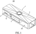
- the first preferred embodiment of a portable interface device assembly 100 includes an interface device 1 and a payment card 10.
- the payment card 10 is to be coupled to the interface device 1 so as to enable an electronic device 9 to access the payment card 10 through the interface device 1.
- Figure 1 illustrates the interface device 1 being in a retracted state.
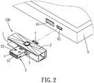
- Figure 2 illustrates the interface device 1 being in an exposed state.
- the electronic device 9 may be embodied as a device (such as a personal computer, a laptop computer, a mobile phone, a smart television, or the like) that includes an interface compatible to the interface device 1.
- the electronic device 9 After a connection has been established between the electronic device 9 and the payment card 10, the electronic device 9 is able to proceed to handle functionalities associated with the payment card 10, such as a transaction. Since the feature of the present invention does not reside in the operations related to the manner in which the electronic device 9 handles the functionalities, details thereof will be omitted herein for the sake of brevity.
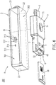
- the interface device 1 includes a housing 2, a switching unit 3, a circuit board 4, a first connecting interface 5, a card interface 6, and a second connecting interface 7.
- first connecting interface 5, the card interface 6, and the second connecting interface 7 are integrated with the circuit board 4. In other embodiments, additional connecting interfaces may be further integrated onto the circuit board 4.
- the housing 2 has an elongated shape with a pair of long sides and a pair of short sides (see Figure 3 ), and includes a top wall 21, a bottom wall 22 and a pair of side walls 23. Each of the side walls 23 is disposed at a respective one of the short sides to interconnect the top wall 21 and the bottom wall 22.
- a through hole 231 may be formed in one of the side walls 23 for allowing a locking mechanism (e.g., awire) to extend therethrough, thus enabling the interface device 1 to be attached to other objects, such as a purse or a portable device, as an accessory item.
- a locking mechanism e.g., awire
- the top wall 21 and the bottom wall 22 are not connected to each other at the long sides, thereby forming two openings 201, 202 at the long sides, respectively.
- the switching unit 3 is movably connected to the housing 2, and includes a hollow base 31 and a frame 32 extending from a side of the base 31. In this embodiment, the switching unit 3 is rotatably connected to the housing 2. Operation of the switching unit 3 will be described in detail in the succeeding paragraphs.
- the circuit board 4 has opposite first and second surfaces 41, 42, and has an elongated shape with a pair of long sides and a pair of short sides, similar to the housing 2.
- the circuit board 4 is mounted on the switching unit 3. Specifically, a part of the circuit board 4 is contained in the base 31, and another part of the circuit board 4 engages the frame 32. Consequently, the circuit board 4 can be brought to move relative to the housing 2 by the switching unit 3.
- the first connecting interface 5 is provided on one of the short sides of the circuit board 4 at the frame 32 of the switching unit 3, and is configured to be electrically connected to a first socket 91 of the electronic device 9.
- the first connecting interface 5 may comply with the universal serial bus (USB) 2.0 or USB 3.0 standard, while the first socket 91 may be a USB socket that supports the USB 2.0 and USB 3.0 standard (see Figure 2 ).
- Other connectivity standards may be employed to implement the first connecting interface 5 for connecting with various sockets of the electronic device 9.
- the card interface 6 includes a card terminal set 61 that is disposed on the circuit board 4.
- the first connecting interface 5 includes a first terminal set 51 disposed on the circuit board 4, and a first shell member 52.
- the first shell member 52 is connected to the switching unit 3, and surrounds the first terminal set 51 and the card terminal set 61.
- the first shell member 52 and the second surface 42 of the circuit board 4 cooperate to define a card slot 62 for containing the payment card 10, thereby enabling electrical connection between the payment card 10 and the card terminal set 61.
- the payment card 10 is embodied using a micro Secure Digital (SD) card, and includes a plurality of standard pins 11 and three near field communication (NFC) pins 12 (see Figure 3 ).
- SD micro Secure Digital
- NFC near field communication
- the payment card 10 is incorporated with an NFC antenna, and supports NFC communication functionalities.
- the card terminal set 61 includes a plurality of signal terminals 611 and three NFC terminals 612. Referring to Figure 6 , eight signal terminals 611 are incorporated.
- the signal terminals 611 are spaced apart from each other, are arranged in a row, and are electrically and respectively connected to the standard pins 11 of the payment card 10.
- the NFC terminals 612 conform with the NFC specifications ("SD Specifications Part 1 NFC Interface Simplified Addendum" issued by the SD Card Association).
- the NFC terminals 612 are spaced apart from one another, are arranged in a different row with respect to the row of the signal terminals 611, and are electrically and respectively connected to the NFC pins 12 of the payment card 10.
- the payment card 10 coupled to the interface device 1 is enabled to interact with electronic devices that support NFC communication functionalities.
- the interface device 1 may be provided with an NFC antenna electrically connected to the NFC terminals 612, so as to cooperate with the electronic device 9 to execute the NFC communication functionalities.
- the second connecting interface 7 is provided on the other one of the short sides of the circuit board 4 opposite to the first connecting interface 5, and is different from the first connecting interface 5.
- the first connecting interface 5 complies with the USB 2.0 or USB 3.0 standard
- the second connecting interface 7 may comply with microUSB or miniUSB standard.
- the second connecting interface 7 may be configured to be electrically connected to a second socket 92 of the electronic device 9 (see Figure 2 ), and includes an insulated base 71, a second terminal set 72, and a second shell member 73.
- the insulated base 71 is fixed on the other one of the short sides of the circuit board 4.
- the second terminal set 72 is disposed on the insulated base 71 with a portion that is in electrical contact with the circuit board 4.
- the second shell member 73 is connected to the insulated base 71 and covers the second terminal set 72.
- the top wall 21 of the housing 2 includes a top inner wall 211, and a top shaft 212 protruding perpendicularly from the top inner wall 211.
- the top shaft 212 includes two spaced-apart top shaft parts 213, which can be slightly brought toward each other when a clamping force is applied thereto.
- the bottom wall 22 of the housing 2 includes a bottom inner wall 221, and a bottom shaft 222 protruding perpendicularly from the bottom inner wall 221 and registered with the top shaft 212.
- the base 31 of the switching unit 3 is further formed with a first shaft hole 33 for rotatably receiving the top shaft 212, and a second shaft hole 34 for rotatably receiving the bottom shaft 222.
- the switching unit 3 is enabled to rotate relative to the housing 2, allowing the first connecting interface 5 and the second connecting interface 7 to be retracted within or exposed from the housing 2. That is, by virtue of the above configuration, the interface device 1 is operable to switch between the retracted state, in which the first connecting interface 5 and the second connecting interface 7 are contained in the housing 2 (see Figure 1 ), and the exposed state, in which the first connecting interface 5 and the second connecting interface 7 protrude from the housing 2 (see Figure 2 ).
- the circuit board 4 (along with the first connecting interface 5, the card interface 6 and the second connecting interface 7 integrated thereon) is substantially parallel to the housing 2, containing the first connecting interface 5 and the second connecting interface 7 in the housing 2.
- the circuit board 4 is substantially perpendicular to the housing 2, resulting in the first connecting interface 5 and the second connecting interface 7 extending out of the housing 2 respectively through the openings 201, 202.
- various configurations may be applied to the housing 2 and the switching unit 3 to achieve the same effect.
- only one pair of shaft 212 and first shaft hole 33 may be sufficient.
- the housing 2 further includes a first positioning unit 214 (see Figure 4 ) that is disposed on the inner wall 211, and that is spaced apart from the top shaft 212.
- the switching unit 3 further includes a plurality of second positioning units 35 that are disposed on the base 31 and that are shaped to engage the first positioning unit 214.
- the first positioning unit 214 is a protrusion
- each of the second positioning units 35 is an engaging hole that is able to engage the protrusion.
- three second positioning units 35 are provided.
- the second positioning units 35 are arranged around and spaced apart from the first shaft hole 33, and are angularly spaced apart from each other with respect to the first shaft hole 33 as a center. Adjacent two of the second positioning units 35 are angularly spaced apart from each other by 90 degrees with respect to the first shaft hole 33.
- the first positioning unit 214 engages one of the second positioning units 35 (i.e., 35a). Alternatively, when the interface device 1 is in the exposed state, the first positioning unit 214 engages another one of the second positioning units 35 (i.e., 35b or 35c).
- positioning of the switching unit 3 is done by the engagement between the first positioning unit 214 and the one of the second positioning units 35, arresting rotational movement of the switching unit 3 relative to the housing 2, until a force sufficient to disengage the first positioning unit 214 from the one of the second positioning units 35 is applied.
- the payment card 10 which is a microSD card
- the payment card 10 is first inserted into the card slot 62 of the interface device 1, and the switching unit 3 may be rotated from the retracted state to the exposed state (i.e., by 90 degrees).
- the interface device 1 is coupled to the electronic device 9 via the first socket 91 using the first connecting interface 5, or via the second socket 92 using the second connecting interface 7. In this manner, the electronic device 9 is operable to access the payment card 10 even though the electronic device 9 lacks the proper interface for accessing the payment card 10 directly.
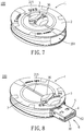
- Figures 7 to 9 illustrate an example of a portable interface device assembly 100 not according to the present invention.
- Figure 7 illustrates the interface device 1 of the example in the retracted state.
- Figure 8 illustrates the interface device 1 of the example in a first exposed state, in which the first connecting interface 5 is exposed out of the housing 2.
- Figure 9 illustrates the interface device 1 of the example in a second exposed state, in which the second connecting interface 7 is exposed out of the housing 2.
- the main difference between this example and the previous embodiment resides in the configuration of the housing 2 and the interactions between the housing 2 and the switching unit 3.
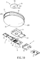
- the housing 2 is substantially disk-shaped, and includes a pair of circular walls (namely, a top wall 21 and a bottom wall 22), and a peripheral wall 24 that interconnects the circular walls 21 and 22 and that is formed with a pair of openings 203 and 204.
- the top wall 21 is formed with a slide groove 215 radially extending and penetrating the top wall 21.
- the openings 203 and 204 are formed near respective ends of the slide groove 215, and are radially opposite to each other.
- the switching unit 3 further has a user-operable unit 36 disposed on the top wall 21, and a base 31 disposed in the housing 2 for mounting the circuit board 4.
- the user-operable unit 36 has a manual operation member 361, a restricting member 362 and an interconnecting member 363.
- the manual operation member 361 is disposed outside the housing 2.
- the restricting member 362 is disposed in the housing 2, and is connected to the base 31. In this example, this is done by disposing the restricting member 362 fittingly in a retaining hole 37 formed in the base 31.
- the interconnecting member 363 is dimensioned to have a diameter slightly smaller or equal to a width of the slide groove 215 for allowing the interconnecting member 363 to slide within the slide groove 215.
- a length of the interconnecting member 363 is configured to be slightly greater than a thickness of the top wall 21.
- Both the manual operation member 361 and the restricting member 362 are dimensioned to be unable to move through the slide groove 215 to prevent the user-operable unit 36 from disengaging the housing 2.
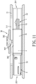
- Figures 7 and 11 illustrate the interface device 1 in the retracted state.
- the user-operable unit 36 is in an inner position of the top wall 21 radially away from the peripheral wall 24. That is, the user-operable unit 36 is substantially in the center of the disk-shaped top wall 21, and in the middle of the slide groove 215.
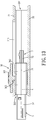
- Figures 8 and 13 illustrate the interface device 1 in the first exposed state.
- the user-operable unit 36 (along with the circuit board 4 and the components integrated thereon) is radially moved (for example, by the user) along the slide groove 215 toward the opening 203 in the peripheral wall 24 to a first outer position on the top wall 21, and the first connecting interface 5 extends out of the housing 2 through the opening 203.
- Figures 9 and 14 illustrate the interface device 1 in the second exposed state.
- the user-operable unit 36 (along with the circuit board 4 and the components integrated thereon) is radially moved along the slide groove 215 toward the opening 204 in the peripheral wall 24 to a second outer position on the top wall 21, and the second connecting interface 7 extends out of the housing 2 through the opening 204.
- the interface device 1 and the payment card 10 are considered as separate components, when the interface device 1 has the payment card 10 inserted therein, the combination of the interface device 1 and the payment card 10 may be considered to be a portable interface device assembly 100.
- embodiments of the present invention provide multiple interfaces for coupling the payment card 10 to the electronic device 9 that may not include the proper interface to access the payment card 10 directly.
- the interface device 1 may incorporate the NFC standard to allow communication between the payment card 10 and the electronic device 9 using the NFC standard.
- the interface device 1 may be switched between the retracted state and the exposed state, and undesired external collision with internal components may be prevented.
Landscapes
- Engineering & Computer Science (AREA)
- Physics & Mathematics (AREA)
- General Physics & Mathematics (AREA)
- Theoretical Computer Science (AREA)
- Microelectronics & Electronic Packaging (AREA)
- Artificial Intelligence (AREA)
- Computer Vision & Pattern Recognition (AREA)
- Computer Hardware Design (AREA)
- Coupling Device And Connection With Printed Circuit (AREA)
- Details Of Connecting Devices For Male And Female Coupling (AREA)
- Telephone Set Structure (AREA)
Description
- This application claims priority of
Taiwanese Application No. 102217086, filed on September 11, 2013 - The invention relates to an interface device, more particularly to a portable interface device assembly that includes the interface device for serving as an interface between a payment card and an electronic device.
-
US2009/0255991 discloses a card reader which includes a hollow base provided with a USB standard metal casing at one side, and an electric module mounted in the USB standard metal casing and the hollow base and defining with the USB standard metal casing in an electronic card receiving space for accommodating an electric card such that the accommodated electronic card is insertable with the USB standard metal casing into a USB port of an electronic apparatus for two-way data transfer (reading or storing) between the electronic card and the electronic apparatus. -
US7575481 discloses a USB plug with a built-in card-reading slot having a metal housing meeting the specification of a USB A-Type plug and an isolation substrate enclosed within the metal housing. -
US2009/0089496 discloses a dual interface data storage apparatus. - A conventional portable peripheral device (e.g., a flash disk) is usually equipped with a connector for coupling with an electronic device, such as a personal computer. The conventional portable peripheral device may include a housing, a circuit board disposed within the housing, a storage unit disposed on the circuit board, and a connector coupled to the circuit board and partly exposed from the housing. In operation, the connector is coupled to the electronic device, allowing the electronic device to access the storage unit.
- The interface device may also serve as an interface between other electronic components (e.g., a memory card, a payment card, etc.) having interfaces not compatible with the electronic device.
- Moreover, it may be desired that the interface device be well-protected from external collisions, in order to prevent the interface device from malfunctioning.
- Therefore, one object of the present invention is to provide an interface device in accordance with
claim 1. That serves as an interface between a payment card and an electronic device. - Accordingly, an interface device of the present invention is for coupling a payment card to an electronic device so as to allow the electronic device to access the payment card via the interface device. The interface device comprises a housing, a switching unit, a circuit board, a card interface, and a connecting interface.
- The switching unit is movably connected to the housing. The circuit board is mounted on the switching unit and is brought to move relative to the housing by the switching unit. The card interface includes a card terminal set disposed on the circuit board.
- The connecting interface is configured to be electrically connected to a socket of the electronic device, and includes a terminal set and a shell member. The terminal set is disposed on the circuit board. The shell member is connected to the switching unit and surrounds the terminal set and the card terminal set. The shell member and the circuit board cooperate to define a card slot for containing the payment card therein, such that the payment card is electrically connected to the card terminal set.
- The interface device is operable to switch between a retracted state, in which the connecting interface is contained in the housing, and an exposed state, in which the connecting interface protrudes from the housing.
- Another object of the present invention is to provide a portable interface device assembly. Accordingly, a portable interface device assembly of the present invention is configured to be coupled to an electronic device, and comprises an interface device and a payment card. The payment card is coupled to the interface device so as to enable the electronic device to access the payment card through the interface device. The interface device includes a housing, a switching unit, a circuit board, a card interface, and a connecting interface.
- The switching unit is movably connected to the housing. The circuit board is mounted on the switching unit and is brought to move relative to the housing by the switching unit. The card interface includes a card terminal set disposed on the circuit board.
- The connecting interface is configured to be electrically connected to a socket of the electronic device, and includes a terminal set and a shell member. The terminal set is disposed on the circuit board. The shell member is connected to the switching unit and surrounds the terminal set and the card terminal set. The shell member and the circuit board cooperate to define a card slot for containing the payment card therein, such that the payment card is electrically connected to the card terminal set.
- The interface device is operable to switch between a retracted state, in which the connecting interface is contained in the housing, and an exposed state, in which the connecting interface protrudes from the housing.
- Other features and advantages of the present invention will become apparent in the following detailed description of the preferred embodiments with reference to the accompanying drawings, of which:
-
Figure 1 is a perspective view of a first preferred embodiment of a portable interface device assembly according to the invention, where an interface device thereof is in a retracted state; -
Figure 2 is a perspective view of the portable interface device assembly of the first preferred embodiment, where the interface device is in an exposed state; -
Figures 3 and4 are exploded perspective views of the portable interface device assembly of the first preferred embodiment, viewed from different angles; -
Figures 5 and6 are exploded perspective views of the interface device of the first preferred embodiment viewed from different viewing angles, with a housing being omitted; -
Figure 7 is a perspective view of an example portable interface device assembly, not according to the invention, where an interface device thereof is in a retracted state; -
Figures 8 and9 are perspective views illustrating the portable interface device assembly of the example, where the interface device is in a first exposed state and a second exposed state, respectively; -
Figure 10 is an exploded perspective view of the portable interface device assembly of the example; -
Figure 11 is a sectional view illustrating the interface device of the example in the retracted state; -
Figure 12 is an exploded perspective view of the interface device of the example viewed from a viewing angle different from that ofFigure 10 and with a housing being omitted; and -
Figure 13 and14 are sectional views illustrating the interface device of the example being in the first exposed state and the second exposed state, respectively. - Before the present invention is described in greater detail, it should be noted that like elements are denoted by the same reference numerals throughout the disclosure. As shown in
Figures 1 and2 , the first preferred embodiment of a portableinterface device assembly 100 according to the present invention includes aninterface device 1 and apayment card 10. Thepayment card 10 is to be coupled to theinterface device 1 so as to enable an electronic device 9 to access thepayment card 10 through theinterface device 1. -
Figure 1 illustrates theinterface device 1 being in a retracted state.Figure 2 illustrates theinterface device 1 being in an exposed state. - The electronic device 9 may be embodied as a device (such as a personal computer, a laptop computer, a mobile phone, a smart television, or the like) that includes an interface compatible to the
interface device 1. - After a connection has been established between the electronic device 9 and the
payment card 10, the electronic device 9 is able to proceed to handle functionalities associated with thepayment card 10, such as a transaction. Since the feature of the present invention does not reside in the operations related to the manner in which the electronic device 9 handles the functionalities, details thereof will be omitted herein for the sake of brevity. - Further referring to
Figures 3 and4 , theinterface device 1 includes ahousing 2, aswitching unit 3, acircuit board 4, a first connectinginterface 5, acard interface 6, and a second connectinginterface 7. - In this embodiment, the first connecting
interface 5, thecard interface 6, and the second connectinginterface 7 are integrated with thecircuit board 4. In other embodiments, additional connecting interfaces may be further integrated onto thecircuit board 4. - The
housing 2 has an elongated shape with a pair of long sides and a pair of short sides (seeFigure 3 ), and includes atop wall 21, abottom wall 22 and a pair ofside walls 23. Each of theside walls 23 is disposed at a respective one of the short sides to interconnect thetop wall 21 and thebottom wall 22. A throughhole 231 may be formed in one of theside walls 23 for allowing a locking mechanism (e.g., awire) to extend therethrough, thus enabling theinterface device 1 to be attached to other objects, such as a purse or a portable device, as an accessory item. - The
top wall 21 and thebottom wall 22 are not connected to each other at the long sides, thereby forming twoopenings - The
switching unit 3 is movably connected to thehousing 2, and includes ahollow base 31 and aframe 32 extending from a side of thebase 31. In this embodiment, theswitching unit 3 is rotatably connected to thehousing 2. Operation of the switchingunit 3 will be described in detail in the succeeding paragraphs. - Further referring to
Figures 5 and6 , thecircuit board 4 has opposite first andsecond surfaces housing 2. Thecircuit board 4 is mounted on theswitching unit 3. Specifically, a part of thecircuit board 4 is contained in thebase 31, and another part of thecircuit board 4 engages theframe 32. Consequently, thecircuit board 4 can be brought to move relative to thehousing 2 by theswitching unit 3. - The first connecting
interface 5 is provided on one of the short sides of thecircuit board 4 at theframe 32 of theswitching unit 3, and is configured to be electrically connected to afirst socket 91 of the electronic device 9. The first connectinginterface 5 may comply with the universal serial bus (USB) 2.0 or USB 3.0 standard, while thefirst socket 91 may be a USB socket that supports the USB 2.0 and USB 3.0 standard (seeFigure 2 ). Other connectivity standards may be employed to implement the first connectinginterface 5 for connecting with various sockets of the electronic device 9. - The
card interface 6 includes a card terminal set 61 that is disposed on thecircuit board 4. The first connectinginterface 5 includes a first terminal set 51 disposed on thecircuit board 4, and afirst shell member 52. Thefirst shell member 52 is connected to theswitching unit 3, and surrounds the first terminal set 51 and the card terminal set 61. - The
first shell member 52 and thesecond surface 42 of thecircuit board 4 cooperate to define acard slot 62 for containing thepayment card 10, thereby enabling electrical connection between thepayment card 10 and the card terminal set 61. - Specifically, in this embodiment, the
payment card 10 is embodied using a micro Secure Digital (SD) card, and includes a plurality ofstandard pins 11 and three near field communication (NFC) pins 12 (seeFigure 3 ). In other words, thepayment card 10 is incorporated with an NFC antenna, and supports NFC communication functionalities. - Accordingly, the card terminal set 61 includes a plurality of
signal terminals 611 and threeNFC terminals 612. Referring toFigure 6 , eightsignal terminals 611 are incorporated. - The
signal terminals 611 are spaced apart from each other, are arranged in a row, and are electrically and respectively connected to the standard pins 11 of thepayment card 10. TheNFC terminals 612 conform with the NFC specifications ("SD Specifications Part 1 NFC Interface Simplified Addendum" issued by the SD Card Association). In this embodiment, theNFC terminals 612 are spaced apart from one another, are arranged in a different row with respect to the row of thesignal terminals 611, and are electrically and respectively connected to the NFC pins 12 of thepayment card 10. - As a result, the
payment card 10 coupled to theinterface device 1 is enabled to interact with electronic devices that support NFC communication functionalities. In embodiments where thepayment card 10 is not incorporated with an NFC antenna, theinterface device 1 may be provided with an NFC antenna electrically connected to theNFC terminals 612, so as to cooperate with the electronic device 9 to execute the NFC communication functionalities. - The second connecting
interface 7 is provided on the other one of the short sides of thecircuit board 4 opposite to the first connectinginterface 5, and is different from the first connectinginterface 5. For example, while the first connectinginterface 5 complies with the USB 2.0 or USB 3.0 standard, the second connectinginterface 7 may comply with microUSB or miniUSB standard. In practice, the second connectinginterface 7 may be configured to be electrically connected to asecond socket 92 of the electronic device 9 (seeFigure 2 ), and includes an insulatedbase 71, a second terminal set 72, and asecond shell member 73. - The
insulated base 71 is fixed on the other one of the short sides of thecircuit board 4. The second terminal set 72 is disposed on theinsulated base 71 with a portion that is in electrical contact with thecircuit board 4. Thesecond shell member 73 is connected to theinsulated base 71 and covers the second terminal set 72. - Referring to
Figures 3 and4 , thetop wall 21 of thehousing 2 includes a topinner wall 211, and atop shaft 212 protruding perpendicularly from the topinner wall 211. Thetop shaft 212 includes two spaced-aparttop shaft parts 213, which can be slightly brought toward each other when a clamping force is applied thereto. Thebottom wall 22 of thehousing 2 includes a bottominner wall 221, and abottom shaft 222 protruding perpendicularly from the bottominner wall 221 and registered with thetop shaft 212. - The
base 31 of theswitching unit 3 is further formed with afirst shaft hole 33 for rotatably receiving thetop shaft 212, and asecond shaft hole 34 for rotatably receiving thebottom shaft 222. - Using the above configuration, the
switching unit 3 is enabled to rotate relative to thehousing 2, allowing the first connectinginterface 5 and the second connectinginterface 7 to be retracted within or exposed from thehousing 2. That is, by virtue of the above configuration, theinterface device 1 is operable to switch between the retracted state, in which the first connectinginterface 5 and the second connectinginterface 7 are contained in the housing 2 (seeFigure 1 ), and the exposed state, in which the first connectinginterface 5 and the second connectinginterface 7 protrude from the housing 2 (seeFigure 2 ). - When the
interface device 1 is in the retracted state, the circuit board 4 (along with the first connectinginterface 5, thecard interface 6 and the second connectinginterface 7 integrated thereon) is substantially parallel to thehousing 2, containing the first connectinginterface 5 and the second connectinginterface 7 in thehousing 2. When theinterface device 1 is in the exposed state, thecircuit board 4 is substantially perpendicular to thehousing 2, resulting in the first connectinginterface 5 and the second connectinginterface 7 extending out of thehousing 2 respectively through theopenings - In other embodiments, various configurations may be applied to the
housing 2 and theswitching unit 3 to achieve the same effect. For example, only one pair ofshaft 212 andfirst shaft hole 33 may be sufficient. - In order to position the
switching unit 3 with respect to thehousing 2, additional positioning mechanisms may be employed. In this embodiment, thehousing 2 further includes a first positioning unit 214 (seeFigure 4 ) that is disposed on theinner wall 211, and that is spaced apart from thetop shaft 212. Theswitching unit 3 further includes a plurality ofsecond positioning units 35 that are disposed on thebase 31 and that are shaped to engage thefirst positioning unit 214. Particularly, thefirst positioning unit 214 is a protrusion, and each of thesecond positioning units 35 is an engaging hole that is able to engage the protrusion. - Referring to
Figure 5 , in this embodiment, three second positioning units 35 (denoted as 35a, 35b and 35c respectively) are provided. Thesecond positioning units 35 are arranged around and spaced apart from thefirst shaft hole 33, and are angularly spaced apart from each other with respect to thefirst shaft hole 33 as a center. Adjacent two of thesecond positioning units 35 are angularly spaced apart from each other by 90 degrees with respect to thefirst shaft hole 33. - When the
interface device 1 is in the retracted state, thefirst positioning unit 214 engages one of the second positioning units 35 (i.e., 35a). Alternatively, when theinterface device 1 is in the exposed state, thefirst positioning unit 214 engages another one of the second positioning units 35 (i.e., 35b or 35c). - When engaging one of the
second positioning units 35, positioning of theswitching unit 3 is done by the engagement between thefirst positioning unit 214 and the one of thesecond positioning units 35, arresting rotational movement of theswitching unit 3 relative to thehousing 2, until a force sufficient to disengage thefirst positioning unit 214 from the one of thesecond positioning units 35 is applied. - While three
second positioning units 35 are employed in this embodiment, various numbers of thesecond positioning units 35 may be incorporated in other embodiments to accommodate different requirements/applications. - In operation, when it is desired to access the payment card 10 (which is a microSD card) using an electronic device 9 having only the first socket 91 (a standard USB socket) and the second socket 92 (a microUSB socket) and no microSD card reader, the
payment card 10 is first inserted into thecard slot 62 of theinterface device 1, and theswitching unit 3 may be rotated from the retracted state to the exposed state (i.e., by 90 degrees). Then, theinterface device 1 is coupled to the electronic device 9 via thefirst socket 91 using the first connectinginterface 5, or via thesecond socket 92 using the second connectinginterface 7. In this manner, the electronic device 9 is operable to access thepayment card 10 even though the electronic device 9 lacks the proper interface for accessing thepayment card 10 directly. -
Figures 7 to 9 illustrate an example of a portableinterface device assembly 100 not according to the present invention.Figure 7 illustrates theinterface device 1 of the example in the retracted state.Figure 8 illustrates theinterface device 1 of the example in a first exposed state, in which the first connectinginterface 5 is exposed out of thehousing 2.Figure 9 illustrates theinterface device 1 of the example in a second exposed state, in which the second connectinginterface 7 is exposed out of thehousing 2. - The main difference between this example and the previous embodiment resides in the configuration of the
housing 2 and the interactions between thehousing 2 and theswitching unit 3. - Particularly, the
housing 2 is substantially disk-shaped, and includes a pair of circular walls (namely, atop wall 21 and a bottom wall 22), and aperipheral wall 24 that interconnects thecircular walls openings top wall 21 is formed with aslide groove 215 radially extending and penetrating thetop wall 21. Theopenings slide groove 215, and are radially opposite to each other. - Referring to
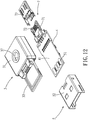
Figures 10 to 12 , theswitching unit 3 further has a user-operable unit 36 disposed on thetop wall 21, and a base 31 disposed in thehousing 2 for mounting thecircuit board 4. - The user-
operable unit 36 has amanual operation member 361, a restrictingmember 362 and an interconnectingmember 363. Themanual operation member 361 is disposed outside thehousing 2. - The restricting
member 362 is disposed in thehousing 2, and is connected to thebase 31. In this example, this is done by disposing the restrictingmember 362 fittingly in a retaininghole 37 formed in thebase 31. - The interconnecting
member 363 is dimensioned to have a diameter slightly smaller or equal to a width of theslide groove 215 for allowing the interconnectingmember 363 to slide within theslide groove 215. A length of the interconnectingmember 363 is configured to be slightly greater than a thickness of thetop wall 21. Both themanual operation member 361 and the restrictingmember 362 are dimensioned to be unable to move through theslide groove 215 to prevent the user-operable unit 36 from disengaging thehousing 2. -
Figures 7 and11 illustrate theinterface device 1 in the retracted state. Here, the user-operable unit 36 is in an inner position of thetop wall 21 radially away from theperipheral wall 24. That is, the user-operable unit 36 is substantially in the center of the disk-shapedtop wall 21, and in the middle of theslide groove 215. -
Figures 8 and13 illustrate theinterface device 1 in the first exposed state. Here, the user-operable unit 36 (along with thecircuit board 4 and the components integrated thereon) is radially moved (for example, by the user) along theslide groove 215 toward theopening 203 in theperipheral wall 24 to a first outer position on thetop wall 21, and the first connectinginterface 5 extends out of thehousing 2 through theopening 203. -
Figures 9 and14 illustrate theinterface device 1 in the second exposed state. Here, the user-operable unit 36 (along with thecircuit board 4 and the components integrated thereon) is radially moved along theslide groove 215 toward theopening 204 in theperipheral wall 24 to a second outer position on thetop wall 21, and the second connectinginterface 7 extends out of thehousing 2 through theopening 204. - While, in the previous embodiments, the
interface device 1 and thepayment card 10 are considered as separate components, when theinterface device 1 has thepayment card 10 inserted therein, the combination of theinterface device 1 and thepayment card 10 may be considered to be a portableinterface device assembly 100. - To sum up, embodiments of the present invention provide multiple interfaces for coupling the
payment card 10 to the electronic device 9 that may not include the proper interface to access thepayment card 10 directly. Additionally, theinterface device 1 may incorporate the NFC standard to allow communication between thepayment card 10 and the electronic device 9 using the NFC standard. Moreover, theinterface device 1 may be switched between the retracted state and the exposed state, and undesired external collision with internal components may be prevented.
Claims (7)
- An interface device (1) for coupling a payment card (10) to an electronic device (9) so as to allow the electronic device (9) to access the payment card (10) via said interface device (1), said interface device (1) including:a housing (2);a switching unit (3) movably connected to said housing (2) ;a circuit board (4) mounted on said switching unit (3) and brought to move relative to said housing (2) by said switching unit (3);a card interface (6) including a card terminal set (61) disposed on said circuit board (4); anda first connecting interface (5) configured to be electrically connected to a first socket (91) of the electronic device (9), and including a first terminal set (51) disposed on said circuit board (4) and a first shell member (52) connected to said switching unit (3) and surrounding said first terminal set (51) and said card terminal set (61), said first shell member (52) and said circuit board (4) cooperating to define a card slot (62) for containing said payment card (10) therein such that said payment card (10) is electrically connected to said card terminal set (61);wherein said interface device (1) is operable to switch between a retracted state, in which said first connecting interface (5) is contained in said housing (2), and an exposed state, in which said first connecting interface (5) protrudes from said housing (2);wherein:said housing (2) has an elongated shape with a pair of long sides, each of said long sides being formed with an opening (201, 202);said switching unit (3) is rotatably disposed in said housing (2);said circuit board (4) has an elongated shape with a pair of short sides, one of which being provided with said first connecting interface (5);when said interface device (1) is in the retracted state, said circuit board (4) is substantially parallel to said housing (2), containing said connecting interface in said housing (2); andwhen said interface device (1) is in the exposed state, said circuit board (4) is substantially perpendicular to said housing (2), resulting in said first connecting interface (5) extending out of said housing (2) through one of said openings (201).
- The interface device (1) of Claim 1, characterized in that:said circuit board (4) has opposite first and second surfaces (41, 42), said first terminal set (51) is disposed on said first surface (41), and said card terminal set (61) is disposed on said second surface (41); andsaid card slot (62) is defined cooperatively by said second surface (41) and said first shell member (52).
- The interface device (1) of any one of Claims 1 and 2, characterized in that said payment card (10) includes a plurality of standard pins (11) and three near field communication (NFC) pins (12), and said card terminal set (61) includes:a plurality of signal terminals (611) that are spaced apart from each other and are arranged in a row, and that are configured to be electrically and respectively connected to said standard pins (11) of said payment card (10); andtwo NFC terminals (612) that are spaced apart from one another and are arranged in a different row with respect to the row of said signal terminals (611), and that are configured to be electrically and respectively connected to said NFC pins (12) of said payment card (10).
- The interface device (1) of Claim 1, further including a second connecting interface (7) that is different from said first connecting interface (5), that is configured to be electrically connected to a second socket of the electronic device (9), and that includes:an insulated base (71) fixed on the other one of said short sides of said circuit board (4);a second terminal set (72) disposed on said insulated base (71) with a portion that is in electrical contact with said circuit board (4); anda second shell member (73) connected to said insulated base (71) and covering said second terminal set (72);characterized in that, when said interface device (1) is switched to the exposed state, said second connecting interface (7) extends out of said housing (2) through the other one of said openings (202).
- The interface device (1) of any one of Claims 1 and 4, characterized in that:said housing (2) includes an inner wall (211), and a shaft (212) protruding perpendicularly from said inner wall (211); andsaid switching unit (3) includes a base (31), and a shaft hole (33) formed in said base (31) and rotatably receiving said shaft (212).
- The interface device (1) of Claim 5, characterized in that:said housing (2) further includes a first positioning unit (214) that is disposed on said inner wall (211) and that is spaced apart from said shaft (212);said switching unit (3) further includes a plurality of second positioning units (35) that are disposed on said base (31), and that are shaped to engage said first positioning unit (214);said second positioning units (35) are arranged around and spaced apart from said shaft hole (33), and are angularly spaced apart from each other with respect to said shaft hole (33) as a center, adjacent two of said second positioning units (35) being angularly spaced apart from each other by 90 degrees with respect to said shaft hole (33);when said interface device (1) is in the retracted state, said first positioning unit (214) engages one of said second positioning units (35), and when said interface device (1) is in the exposed state, said first positioning unit (214) engages another one of said second positioning units (35).
- A portable interface device assembly (100) configured to be coupled to an electronic device (9), said portable interface device assembly (100) including an interface device (1), and a payment card (10) that is coupled to said interface device (1) so as to enable the electronic device (9) to access said payment card (10) through said interface device (1), characterized in that said interface device (1) is one as claimed in any one of Claim 1 to 6.
Applications Claiming Priority (1)
| Application Number | Priority Date | Filing Date | Title |
|---|---|---|---|
| TW102217086U TWM472261U (en) | 2013-09-11 | 2013-09-11 | Connecting apparatus and portable payment device |
Publications (2)
| Publication Number | Publication Date |
|---|---|
| EP2849123A1 EP2849123A1 (en) | 2015-03-18 |
| EP2849123B1 true EP2849123B1 (en) | 2017-08-02 |
Family
ID=50551770
Family Applications (1)
| Application Number | Title | Priority Date | Filing Date |
|---|---|---|---|
| EP14171341.2A Not-in-force EP2849123B1 (en) | 2013-09-11 | 2014-06-05 | Portable interface device assembly and interface device thereof |
Country Status (6)
| Country | Link |
|---|---|
| US (1) | US9202089B2 (en) |
| EP (1) | EP2849123B1 (en) |
| JP (2) | JP6166236B2 (en) |
| CN (2) | CN104425922B (en) |
| HK (1) | HK1206844A1 (en) |
| TW (1) | TWM472261U (en) |
Families Citing this family (16)
| Publication number | Priority date | Publication date | Assignee | Title |
|---|---|---|---|---|
| TWM472261U (en) * | 2013-09-11 | 2014-02-11 | Chien-Kang Yang | Connecting apparatus and portable payment device |
| US9589265B2 (en) | 2013-09-11 | 2017-03-07 | Chien-Kang Yang | Mobile payment method |
| US9311636B2 (en) | 2013-09-11 | 2016-04-12 | Chien-Kang Yang | Mobile payment method and mobile payment apparatus |
| TWM491197U (en) * | 2014-07-18 | 2014-12-01 | Icothing Technology Ltd | Multi-port type mini computer |
| CN106157037B (en) * | 2014-09-11 | 2020-06-30 | 杨建纲 | Mobile payment method and mobile payment equipment |
| TWM497330U (en) * | 2014-10-01 | 2015-03-11 | Ho E Co Ltd | Flash drive having combined type protective lid |
| TWM497329U (en) * | 2014-10-01 | 2015-03-11 | Ho E Co Ltd | Flash drive with deflection opening/closing protection cover |
| CN104992132A (en) * | 2015-07-09 | 2015-10-21 | 深圳市文鼎创数据科技有限公司 | Card reader for IC card |
| US9966716B2 (en) * | 2015-09-08 | 2018-05-08 | Apple Inc. | Adapter |
| CN109076123B (en) * | 2016-03-14 | 2021-06-01 | 美光科技公司 | Folding device frame for portable device |
| US10847909B2 (en) | 2019-02-21 | 2020-11-24 | Western Digital Technologies, Inc. | Data storage devices and connectors for same |
| DE102019104881B4 (en) * | 2019-02-26 | 2020-12-10 | Pilz Gmbh & Co. Kg | Storage device for the mobile provision of data at a technical facility |
| CN112151081B (en) * | 2019-06-26 | 2022-05-31 | 西部数据技术公司 | Data storage device and connector therefor |
| CN112993702A (en) * | 2021-02-08 | 2021-06-18 | 青岛九日软件科技服务有限责任公司 | Connection interface of intelligent bidirectional memory and control method thereof |
| US11350532B1 (en) * | 2021-04-09 | 2022-05-31 | Vinpower Inc. | Portable data storage device with double rotatable protective swivels |
| CN113611337A (en) * | 2021-06-08 | 2021-11-05 | 哈物实业(上海)有限公司 | Memory fixing device with buffer function |
Family Cites Families (18)
| Publication number | Priority date | Publication date | Assignee | Title |
|---|---|---|---|---|
| TW200612221A (en) * | 2004-10-08 | 2006-04-16 | Compal Electronics Inc | Portable storage device with multiple interfaces |
| KR100625507B1 (en) * | 2005-08-09 | 2006-09-18 | 케이비 테크놀러지 (주) | Smart card reader |
| CN2906998Y (en) * | 2006-03-15 | 2007-05-30 | 元次三科技股份有限公司 | Converter |
| US7500858B2 (en) * | 2006-07-27 | 2009-03-10 | Micron Technology, Inc. | Portable electronic device with built-in terminal cover structure |
| FI20065783A0 (en) * | 2006-12-08 | 2006-12-08 | Nokia Corp | Signal pre-distortion in radio transmitters |
| US7740494B2 (en) | 2007-08-30 | 2010-06-22 | Phison Electronics Corp. | Data storage apparatus |
| US7778037B2 (en) * | 2007-09-27 | 2010-08-17 | Phison Electronics Corp. | Dual-interface data storage apparatus |
| US7631232B2 (en) | 2007-09-28 | 2009-12-08 | Inventec Corporation | Parallel burning system and method |
| US8500467B2 (en) * | 2007-10-30 | 2013-08-06 | Super Talent Electronics, Inc. | Flash drive with swivel cover |
| CN201160001Y (en) * | 2008-02-29 | 2008-12-03 | 智晟电子股份有限公司 | Improved card reader |
| TW200935319A (en) | 2008-04-11 | 2009-08-16 | Chant Sincere Co Ltd | A card reader |
| US7575481B1 (en) * | 2008-12-24 | 2009-08-18 | Chen-Ya Liu | USB plug with a built-in-card-reading slot |
| TWM388065U (en) | 2010-03-17 | 2010-09-01 | Dong Wei Industry Ltd Company | Rotary and telescopic storage device |
| US20130214701A1 (en) * | 2010-06-17 | 2013-08-22 | Light Bohrd, LLC | Systems and methods for luminescent display |
| TWI401063B (en) * | 2011-05-25 | 2013-07-11 | Nat Univ Tsing Hua | Melatonin suppression extent measuring device |
| CN202512579U (en) * | 2012-01-12 | 2012-10-31 | 曹礼坤 | Multifunctional card reading wristband |
| US9208367B2 (en) * | 2012-11-15 | 2015-12-08 | Hand Held Products | Mobile computer configured to read multiple decodable indicia |
| TWM472261U (en) | 2013-09-11 | 2014-02-11 | Chien-Kang Yang | Connecting apparatus and portable payment device |
-
2013
- 2013-09-11 TW TW102217086U patent/TWM472261U/en not_active IP Right Cessation
-
2014
- 2014-01-02 CN CN201410002950.8A patent/CN104425922B/en not_active Expired - Fee Related
- 2014-01-02 CN CN201420000765.0U patent/CN203690534U/en not_active Expired - Lifetime
- 2014-05-15 US US14/278,850 patent/US9202089B2/en not_active Expired - Fee Related
- 2014-06-05 EP EP14171341.2A patent/EP2849123B1/en not_active Not-in-force
- 2014-09-08 JP JP2014182638A patent/JP6166236B2/en not_active Expired - Fee Related
- 2014-09-08 JP JP2014004791U patent/JP3194405U/en not_active Expired - Fee Related
-
2015
- 2015-07-31 HK HK15107366.4A patent/HK1206844A1/en not_active IP Right Cessation
Non-Patent Citations (1)
| Title |
|---|
| None * |
Also Published As
| Publication number | Publication date |
|---|---|
| JP3194405U (en) | 2014-11-20 |
| TWM472261U (en) | 2014-02-11 |
| US9202089B2 (en) | 2015-12-01 |
| US20150069124A1 (en) | 2015-03-12 |
| EP2849123A1 (en) | 2015-03-18 |
| JP6166236B2 (en) | 2017-07-19 |
| JP2015065167A (en) | 2015-04-09 |
| HK1206844A1 (en) | 2016-01-15 |
| CN104425922B (en) | 2017-02-08 |
| CN104425922A (en) | 2015-03-18 |
| CN203690534U (en) | 2014-07-02 |
Similar Documents
| Publication | Publication Date | Title |
|---|---|---|
| EP2849123B1 (en) | Portable interface device assembly and interface device thereof | |
| TWI477951B (en) | Detachable adapter and handheld device | |
| US9564720B2 (en) | Retractable power plug | |
| US9844149B2 (en) | Wireless communications antenna assembly | |
| EP2757702B1 (en) | Sim card socket and terminal device including the same | |
| US8123566B2 (en) | Electronic device, adapter and receptacle | |
| US9025337B2 (en) | Wireless module and connector apparatus having the same | |
| US9525231B2 (en) | Flash drive with eccentrically rotatable cover | |
| US9519316B2 (en) | Flash drive with attached cover | |
| US9054472B2 (en) | Power adapter with plug member stowable in housing | |
| KR200469127Y1 (en) | case for mobile phone | |
| JP4817271B2 (en) | card reader | |
| US20030045176A1 (en) | Means having rotatable connector for electrical applicance | |
| EP2626959B1 (en) | Integrated electric connector | |
| US6456496B1 (en) | Type III pccard system with full wall modular extendable RJ45/11 connector | |
| TWI598725B (en) | Storage device | |
| JP3149440U (en) | Card reader | |
| WO2017028403A1 (en) | Electronic signature apparatus | |
| KR100533651B1 (en) | Chipcard-Type Combi-Card, Combi-Card Connector For The Same, and RF Electronic-Paying Device Using The Same | |
| TWM532049U (en) | Storage device | |
| KR20140039556A (en) | Usb memory having a 8 pin connector | |
| KR101316777B1 (en) | Usb memory having a micro 5 pin | |
| US20040128419A1 (en) | Direct-coupled serial transmission interface card | |
| KR101787461B1 (en) | Memory card | |
| TWI433407B (en) | Card connector |
Legal Events
| Date | Code | Title | Description |
|---|---|---|---|
| PUAI | Public reference made under article 153(3) epc to a published international application that has entered the european phase |
Free format text: ORIGINAL CODE: 0009012 |
|
| 17P | Request for examination filed |
Effective date: 20140605 |
|
| AK | Designated contracting states |
Kind code of ref document: A1 Designated state(s): AL AT BE BG CH CY CZ DE DK EE ES FI FR GB GR HR HU IE IS IT LI LT LU LV MC MK MT NL NO PL PT RO RS SE SI SK SM TR |
|
| AX | Request for extension of the european patent |
Extension state: BA ME |
|
| R17P | Request for examination filed (corrected) |
Effective date: 20150608 |
|
| RBV | Designated contracting states (corrected) |
Designated state(s): AL AT BE BG CH CY CZ DE DK EE ES FI FR GB GR HR HU IE IS IT LI LT LU LV MC MK MT NL NO PL PT RO RS SE SI SK SM TR |
|
| REG | Reference to a national code |
Ref country code: HK Ref legal event code: DE Ref document number: 1206844 Country of ref document: HK |
|
| 17Q | First examination report despatched |
Effective date: 20160908 |
|
| GRAP | Despatch of communication of intention to grant a patent |
Free format text: ORIGINAL CODE: EPIDOSNIGR1 |
|
| INTG | Intention to grant announced |
Effective date: 20170224 |
|
| GRAS | Grant fee paid |
Free format text: ORIGINAL CODE: EPIDOSNIGR3 |
|
| GRAA | (expected) grant |
Free format text: ORIGINAL CODE: 0009210 |
|
| AK | Designated contracting states |
Kind code of ref document: B1 Designated state(s): AL AT BE BG CH CY CZ DE DK EE ES FI FR GB GR HR HU IE IS IT LI LT LU LV MC MK MT NL NO PL PT RO RS SE SI SK SM TR |
|
| REG | Reference to a national code |
Ref country code: CH Ref legal event code: EP Ref country code: AT Ref legal event code: REF Ref document number: 915238 Country of ref document: AT Kind code of ref document: T Effective date: 20170815 |
|
| REG | Reference to a national code |
Ref country code: IE Ref legal event code: FG4D |
|
| REG | Reference to a national code |
Ref country code: DE Ref legal event code: R096 Ref document number: 602014012437 Country of ref document: DE |
|
| REG | Reference to a national code |
Ref country code: NL Ref legal event code: MP Effective date: 20170802 |
|
| REG | Reference to a national code |
Ref country code: AT Ref legal event code: MK05 Ref document number: 915238 Country of ref document: AT Kind code of ref document: T Effective date: 20170802 |
|
| REG | Reference to a national code |
Ref country code: LT Ref legal event code: MG4D |
|
| PG25 | Lapsed in a contracting state [announced via postgrant information from national office to epo] |
Ref country code: NO Free format text: LAPSE BECAUSE OF FAILURE TO SUBMIT A TRANSLATION OF THE DESCRIPTION OR TO PAY THE FEE WITHIN THE PRESCRIBED TIME-LIMIT Effective date: 20171102 Ref country code: HR Free format text: LAPSE BECAUSE OF FAILURE TO SUBMIT A TRANSLATION OF THE DESCRIPTION OR TO PAY THE FEE WITHIN THE PRESCRIBED TIME-LIMIT Effective date: 20170802 Ref country code: FI Free format text: LAPSE BECAUSE OF FAILURE TO SUBMIT A TRANSLATION OF THE DESCRIPTION OR TO PAY THE FEE WITHIN THE PRESCRIBED TIME-LIMIT Effective date: 20170802 Ref country code: LT Free format text: LAPSE BECAUSE OF FAILURE TO SUBMIT A TRANSLATION OF THE DESCRIPTION OR TO PAY THE FEE WITHIN THE PRESCRIBED TIME-LIMIT Effective date: 20170802 Ref country code: AT Free format text: LAPSE BECAUSE OF FAILURE TO SUBMIT A TRANSLATION OF THE DESCRIPTION OR TO PAY THE FEE WITHIN THE PRESCRIBED TIME-LIMIT Effective date: 20170802 Ref country code: SE Free format text: LAPSE BECAUSE OF FAILURE TO SUBMIT A TRANSLATION OF THE DESCRIPTION OR TO PAY THE FEE WITHIN THE PRESCRIBED TIME-LIMIT Effective date: 20170802 Ref country code: NL Free format text: LAPSE BECAUSE OF FAILURE TO SUBMIT A TRANSLATION OF THE DESCRIPTION OR TO PAY THE FEE WITHIN THE PRESCRIBED TIME-LIMIT Effective date: 20170802 |
|
| PG25 | Lapsed in a contracting state [announced via postgrant information from national office to epo] |
Ref country code: PL Free format text: LAPSE BECAUSE OF FAILURE TO SUBMIT A TRANSLATION OF THE DESCRIPTION OR TO PAY THE FEE WITHIN THE PRESCRIBED TIME-LIMIT Effective date: 20170802 Ref country code: BG Free format text: LAPSE BECAUSE OF FAILURE TO SUBMIT A TRANSLATION OF THE DESCRIPTION OR TO PAY THE FEE WITHIN THE PRESCRIBED TIME-LIMIT Effective date: 20171102 Ref country code: GR Free format text: LAPSE BECAUSE OF FAILURE TO SUBMIT A TRANSLATION OF THE DESCRIPTION OR TO PAY THE FEE WITHIN THE PRESCRIBED TIME-LIMIT Effective date: 20171103 Ref country code: ES Free format text: LAPSE BECAUSE OF FAILURE TO SUBMIT A TRANSLATION OF THE DESCRIPTION OR TO PAY THE FEE WITHIN THE PRESCRIBED TIME-LIMIT Effective date: 20170802 Ref country code: IS Free format text: LAPSE BECAUSE OF FAILURE TO SUBMIT A TRANSLATION OF THE DESCRIPTION OR TO PAY THE FEE WITHIN THE PRESCRIBED TIME-LIMIT Effective date: 20171202 Ref country code: RS Free format text: LAPSE BECAUSE OF FAILURE TO SUBMIT A TRANSLATION OF THE DESCRIPTION OR TO PAY THE FEE WITHIN THE PRESCRIBED TIME-LIMIT Effective date: 20170802 Ref country code: LV Free format text: LAPSE BECAUSE OF FAILURE TO SUBMIT A TRANSLATION OF THE DESCRIPTION OR TO PAY THE FEE WITHIN THE PRESCRIBED TIME-LIMIT Effective date: 20170802 |
|
| REG | Reference to a national code |
Ref country code: FR Ref legal event code: PLFP Year of fee payment: 5 |
|
| PG25 | Lapsed in a contracting state [announced via postgrant information from national office to epo] |
Ref country code: CZ Free format text: LAPSE BECAUSE OF FAILURE TO SUBMIT A TRANSLATION OF THE DESCRIPTION OR TO PAY THE FEE WITHIN THE PRESCRIBED TIME-LIMIT Effective date: 20170802 Ref country code: RO Free format text: LAPSE BECAUSE OF FAILURE TO SUBMIT A TRANSLATION OF THE DESCRIPTION OR TO PAY THE FEE WITHIN THE PRESCRIBED TIME-LIMIT Effective date: 20170802 Ref country code: DK Free format text: LAPSE BECAUSE OF FAILURE TO SUBMIT A TRANSLATION OF THE DESCRIPTION OR TO PAY THE FEE WITHIN THE PRESCRIBED TIME-LIMIT Effective date: 20170802 |
|
| REG | Reference to a national code |
Ref country code: DE Ref legal event code: R097 Ref document number: 602014012437 Country of ref document: DE |
|
| PG25 | Lapsed in a contracting state [announced via postgrant information from national office to epo] |
Ref country code: IT Free format text: LAPSE BECAUSE OF FAILURE TO SUBMIT A TRANSLATION OF THE DESCRIPTION OR TO PAY THE FEE WITHIN THE PRESCRIBED TIME-LIMIT Effective date: 20170802 Ref country code: SK Free format text: LAPSE BECAUSE OF FAILURE TO SUBMIT A TRANSLATION OF THE DESCRIPTION OR TO PAY THE FEE WITHIN THE PRESCRIBED TIME-LIMIT Effective date: 20170802 Ref country code: EE Free format text: LAPSE BECAUSE OF FAILURE TO SUBMIT A TRANSLATION OF THE DESCRIPTION OR TO PAY THE FEE WITHIN THE PRESCRIBED TIME-LIMIT Effective date: 20170802 Ref country code: SM Free format text: LAPSE BECAUSE OF FAILURE TO SUBMIT A TRANSLATION OF THE DESCRIPTION OR TO PAY THE FEE WITHIN THE PRESCRIBED TIME-LIMIT Effective date: 20170802 |
|
| PLBE | No opposition filed within time limit |
Free format text: ORIGINAL CODE: 0009261 |
|
| STAA | Information on the status of an ep patent application or granted ep patent |
Free format text: STATUS: NO OPPOSITION FILED WITHIN TIME LIMIT |
|
| REG | Reference to a national code |
Ref country code: HK Ref legal event code: GR Ref document number: 1206844 Country of ref document: HK |
|
| 26N | No opposition filed |
Effective date: 20180503 |
|
| PG25 | Lapsed in a contracting state [announced via postgrant information from national office to epo] |
Ref country code: SI Free format text: LAPSE BECAUSE OF FAILURE TO SUBMIT A TRANSLATION OF THE DESCRIPTION OR TO PAY THE FEE WITHIN THE PRESCRIBED TIME-LIMIT Effective date: 20170802 |
|
| REG | Reference to a national code |
Ref country code: CH Ref legal event code: PL |
|
| REG | Reference to a national code |
Ref country code: BE Ref legal event code: MM Effective date: 20180630 |
|
| REG | Reference to a national code |
Ref country code: IE Ref legal event code: MM4A |
|
| PG25 | Lapsed in a contracting state [announced via postgrant information from national office to epo] |
Ref country code: MC Free format text: LAPSE BECAUSE OF FAILURE TO SUBMIT A TRANSLATION OF THE DESCRIPTION OR TO PAY THE FEE WITHIN THE PRESCRIBED TIME-LIMIT Effective date: 20170802 Ref country code: LU Free format text: LAPSE BECAUSE OF NON-PAYMENT OF DUE FEES Effective date: 20180605 |
|
| PG25 | Lapsed in a contracting state [announced via postgrant information from national office to epo] |
Ref country code: CH Free format text: LAPSE BECAUSE OF NON-PAYMENT OF DUE FEES Effective date: 20180630 Ref country code: LI Free format text: LAPSE BECAUSE OF NON-PAYMENT OF DUE FEES Effective date: 20180630 Ref country code: IE Free format text: LAPSE BECAUSE OF NON-PAYMENT OF DUE FEES Effective date: 20180605 |
|
| PG25 | Lapsed in a contracting state [announced via postgrant information from national office to epo] |
Ref country code: BE Free format text: LAPSE BECAUSE OF NON-PAYMENT OF DUE FEES Effective date: 20180630 |
|
| PG25 | Lapsed in a contracting state [announced via postgrant information from national office to epo] |
Ref country code: MT Free format text: LAPSE BECAUSE OF NON-PAYMENT OF DUE FEES Effective date: 20180605 |
|
| PG25 | Lapsed in a contracting state [announced via postgrant information from national office to epo] |
Ref country code: TR Free format text: LAPSE BECAUSE OF FAILURE TO SUBMIT A TRANSLATION OF THE DESCRIPTION OR TO PAY THE FEE WITHIN THE PRESCRIBED TIME-LIMIT Effective date: 20170802 |
|
| PG25 | Lapsed in a contracting state [announced via postgrant information from national office to epo] |
Ref country code: HU Free format text: LAPSE BECAUSE OF FAILURE TO SUBMIT A TRANSLATION OF THE DESCRIPTION OR TO PAY THE FEE WITHIN THE PRESCRIBED TIME-LIMIT; INVALID AB INITIO Effective date: 20140605 Ref country code: PT Free format text: LAPSE BECAUSE OF FAILURE TO SUBMIT A TRANSLATION OF THE DESCRIPTION OR TO PAY THE FEE WITHIN THE PRESCRIBED TIME-LIMIT Effective date: 20170802 |
|
| PG25 | Lapsed in a contracting state [announced via postgrant information from national office to epo] |
Ref country code: MK Free format text: LAPSE BECAUSE OF NON-PAYMENT OF DUE FEES Effective date: 20170802 Ref country code: CY Free format text: LAPSE BECAUSE OF FAILURE TO SUBMIT A TRANSLATION OF THE DESCRIPTION OR TO PAY THE FEE WITHIN THE PRESCRIBED TIME-LIMIT Effective date: 20170802 |
|
| PG25 | Lapsed in a contracting state [announced via postgrant information from national office to epo] |
Ref country code: AL Free format text: LAPSE BECAUSE OF FAILURE TO SUBMIT A TRANSLATION OF THE DESCRIPTION OR TO PAY THE FEE WITHIN THE PRESCRIBED TIME-LIMIT Effective date: 20170802 |
|
| PGFP | Annual fee paid to national office [announced via postgrant information from national office to epo] |
Ref country code: DE Payment date: 20210503 Year of fee payment: 8 Ref country code: FR Payment date: 20210429 Year of fee payment: 8 |
|
| PGFP | Annual fee paid to national office [announced via postgrant information from national office to epo] |
Ref country code: GB Payment date: 20210429 Year of fee payment: 8 |
|
| REG | Reference to a national code |
Ref country code: DE Ref legal event code: R119 Ref document number: 602014012437 Country of ref document: DE |
|
| GBPC | Gb: european patent ceased through non-payment of renewal fee |
Effective date: 20220605 |
|
| PG25 | Lapsed in a contracting state [announced via postgrant information from national office to epo] |
Ref country code: FR Free format text: LAPSE BECAUSE OF NON-PAYMENT OF DUE FEES Effective date: 20220630 |
|
| PG25 | Lapsed in a contracting state [announced via postgrant information from national office to epo] |
Ref country code: GB Free format text: LAPSE BECAUSE OF NON-PAYMENT OF DUE FEES Effective date: 20220605 Ref country code: DE Free format text: LAPSE BECAUSE OF NON-PAYMENT OF DUE FEES Effective date: 20230103 |