EP2846467A1 - Output driver circuit - Google Patents
Output driver circuit Download PDFInfo
- Publication number
- EP2846467A1 EP2846467A1 EP13780640.2A EP13780640A EP2846467A1 EP 2846467 A1 EP2846467 A1 EP 2846467A1 EP 13780640 A EP13780640 A EP 13780640A EP 2846467 A1 EP2846467 A1 EP 2846467A1
- Authority
- EP
- European Patent Office
- Prior art keywords
- current
- circuit
- constant
- output
- mos transistor
- Prior art date
- Legal status (The legal status is an assumption and is not a legal conclusion. Google has not performed a legal analysis and makes no representation as to the accuracy of the status listed.)
- Granted
Links
Images


Classifications
-
- G—PHYSICS
- G05—CONTROLLING; REGULATING
- G05F—SYSTEMS FOR REGULATING ELECTRIC OR MAGNETIC VARIABLES
- G05F3/00—Non-retroactive systems for regulating electric variables by using an uncontrolled element, or an uncontrolled combination of elements, such element or such combination having self-regulating properties
- G05F3/02—Regulating voltage or current
- G05F3/08—Regulating voltage or current wherein the variable is DC
- G05F3/10—Regulating voltage or current wherein the variable is DC using uncontrolled devices with non-linear characteristics
- G05F3/16—Regulating voltage or current wherein the variable is DC using uncontrolled devices with non-linear characteristics being semiconductor devices
- G05F3/20—Regulating voltage or current wherein the variable is DC using uncontrolled devices with non-linear characteristics being semiconductor devices using diode- transistor combinations
- G05F3/26—Current mirrors
- G05F3/262—Current mirrors using field-effect transistors only
-
- H—ELECTRICITY
- H02—GENERATION; CONVERSION OR DISTRIBUTION OF ELECTRIC POWER
- H02H—EMERGENCY PROTECTIVE CIRCUIT ARRANGEMENTS
- H02H9/00—Emergency protective circuit arrangements for limiting excess current or voltage without disconnection
- H02H9/02—Emergency protective circuit arrangements for limiting excess current or voltage without disconnection responsive to excess current
-
- H—ELECTRICITY
- H03—ELECTRONIC CIRCUITRY
- H03K—PULSE TECHNIQUE
- H03K17/00—Electronic switching or gating, i.e. not by contact-making and –breaking
- H03K17/08—Modifications for protecting switching circuit against overcurrent or overvoltage
- H03K17/081—Modifications for protecting switching circuit against overcurrent or overvoltage without feedback from the output circuit to the control circuit
- H03K17/0812—Modifications for protecting switching circuit against overcurrent or overvoltage without feedback from the output circuit to the control circuit by measures taken in the control circuit
- H03K17/08122—Modifications for protecting switching circuit against overcurrent or overvoltage without feedback from the output circuit to the control circuit by measures taken in the control circuit in field-effect transistor switches
-
- H—ELECTRICITY
- H03—ELECTRONIC CIRCUITRY
- H03K—PULSE TECHNIQUE
- H03K17/00—Electronic switching or gating, i.e. not by contact-making and –breaking
- H03K17/51—Electronic switching or gating, i.e. not by contact-making and –breaking characterised by the components used
- H03K17/56—Electronic switching or gating, i.e. not by contact-making and –breaking characterised by the components used by the use, as active elements, of semiconductor devices
- H03K17/687—Electronic switching or gating, i.e. not by contact-making and –breaking characterised by the components used by the use, as active elements, of semiconductor devices the devices being field-effect transistors
-
- H—ELECTRICITY
- H03—ELECTRONIC CIRCUITRY
- H03K—PULSE TECHNIQUE
- H03K19/00—Logic circuits, i.e. having at least two inputs acting on one output; Inverting circuits
- H03K19/0175—Coupling arrangements; Interface arrangements
- H03K19/0185—Coupling arrangements; Interface arrangements using field effect transistors only
- H03K19/018507—Interface arrangements
-
- H—ELECTRICITY
- H03—ELECTRONIC CIRCUITRY
- H03K—PULSE TECHNIQUE
- H03K19/00—Logic circuits, i.e. having at least two inputs acting on one output; Inverting circuits
- H03K19/02—Logic circuits, i.e. having at least two inputs acting on one output; Inverting circuits using specified components
- H03K19/173—Logic circuits, i.e. having at least two inputs acting on one output; Inverting circuits using specified components using elementary logic circuits as components
- H03K19/1733—Controllable logic circuits
- H03K19/1737—Controllable logic circuits using multiplexers
-
- H—ELECTRICITY
- H03—ELECTRONIC CIRCUITRY
- H03K—PULSE TECHNIQUE
- H03K2217/00—Indexing scheme related to electronic switching or gating, i.e. not by contact-making or -breaking covered by H03K17/00
- H03K2217/0063—High side switches, i.e. the higher potential [DC] or life wire [AC] being directly connected to the switch and not via the load
-
- H—ELECTRICITY
- H03—ELECTRONIC CIRCUITRY
- H03K—PULSE TECHNIQUE
- H03K2217/00—Indexing scheme related to electronic switching or gating, i.e. not by contact-making or -breaking covered by H03K17/00
- H03K2217/0072—Low side switches, i.e. the lower potential [DC] or neutral wire [AC] being directly connected to the switch and not via the load
-
- H—ELECTRICITY
- H03—ELECTRONIC CIRCUITRY
- H03K—PULSE TECHNIQUE
- H03K2217/00—Indexing scheme related to electronic switching or gating, i.e. not by contact-making or -breaking covered by H03K17/00
- H03K2217/0081—Power supply means, e.g. to the switch driver
Definitions
- the present invention relates to an output driver circuit provided with an overcurrent protection function.
- FIG. 5 is a circuit diagram illustrating the conventional output driver circuit.
- a conventional output driver circuit 50 with an overcurrent protection function includes an NMOS transistor 55, which is an output driver connected to an output terminal 57, a sense resistor 58, which is connected to a current path of the output driver and which monitors an output current, a reference voltage circuit 51, which outputs a reference voltage, a comparator 52, which compares a voltage generated at the sense resistor 58 and the reference voltage, and an NOR circuit 54, which controls the gate of the NMOS transistor 55 according to an output signal of the comparator 52 and a signal of an input terminal 53.
- an NMOS transistor may be connected in place of the sense resistor 58 to provide the same protection (refer to, for example, Japanese Patent Application Laid-Open No. 6-38363 ).
- the conventional output driver circuit with an overcurrent protection function has been posing a problem in that the need for a comparator and a reference voltage circuit inevitably results in a large circuit scale.
- An output driver circuit in accordance with the present invention has been made with a view toward overcoming the aforesaid drawbacks, and an object of the invention is to provide an output driver circuit with an overcurrent protection function, which has a simple circuit configuration and which does not deteriorate the drive capability of an output driver.
- the present invention provides an output driver circuit with an open-drain output, which is provided with an overcurrent protection function, including: a constant-current circuit which supplies a constant current; a constant-current mirror MOS transistor which generates a voltage based on the constant current; a selector circuit which receives a voltage of the constant-current mirror MOS transistor and a voltage of a first supply terminal and outputs one of the received voltages according to a signal supplied to an input terminal of the output driver circuit; an output MOS transistor with a gate thereof connected to an output terminal of the selector circuit, a drain thereof connected to an output terminal of the output driver circuit and a source thereof connected to the first supply terminal, wherein a current flowing between the source and the drain of the output MOS transistor is limited by a voltage based on the constant current.
- the output driver circuit in accordance with the present invention is configured to control the current of the output MOS transistor by the current mirror circuit to implement the overcurrent protection function. This obviates the need for a sense resistor for the source of the output MOS transistor and also obviates the need for a comparator and a reference voltage circuit, thus making it possible to provide an output driver circuit with an overcurrent protection function that has a simple configuration and does not incur deterioration of the drive capability in a normal operation.
- FIG. 1 is a circuit diagram illustrating an output driver circuit of an embodiment.
- An output driver circuit 10 includes a constant-current circuit 11, a constant-current mirror MOS transistor 12, an input terminal 13, a selector circuit 14, and an NMOS transistor 15.
- the gate of the NMOS transistor 15 is connected to the output of the selector circuit 14, the source thereof is connected to a grounding terminal 2, and the drain thereof is connected to an output terminal 17.
- the NMOS transistor 15 is an open-drain type output driver, the output terminal 17 being connected to a supply terminal 3 of a circuit in a subsequent stage through the intermediary of an external pull-up resistor 16.
- the selector circuit 14 If the voltage of the input terminal 13 is "L" level, then the selector circuit 14 outputs the ground voltage VSS. Hence, the NMOS transistor 15 turns off, placing the output terminal 17 of the output driver circuit 10 in a high impedance state. Hence, the output terminal 17 of the output driver circuit 10 is pulled up to a supply voltage VCC of a circuit in the subsequent stage, the output terminal 17 being connected to the input terminal of the circuit in the subsequent stage. In other words, the output driver circuit 10 outputs "H" level to the output terminal 17.
- the constant-current mirror MOS transistor 12 may be provided with an NMOS transistor and a fuse for adjusting current so as to make the current mirror ratio adjustable. Configuring the constant-current mirror MOS transistor 12 in this manner makes it possible to restrain variations in the constant current Iconst and variations in the current mirror ratio. Hence, the accuracy of the current limit value Ilimit can be enhanced.
- the overcurrent protection function can be accomplished in the same manner by using the constant-current mirror MOS transistor 12, a selector circuit 44, and an output MOS transistor 45.
- the output terminal 17 is connected to a grounding terminal 4 of the circuit in a subsequent stage through the intermediary of an external pull-up resistor 16.
- the fuse trimming or the like may be used to add a function for restraining the variations in the current limit value Ilimit.
Landscapes
- Engineering & Computer Science (AREA)
- Physics & Mathematics (AREA)
- Computer Hardware Design (AREA)
- Microelectronics & Electronic Packaging (AREA)
- Computing Systems (AREA)
- General Engineering & Computer Science (AREA)
- Mathematical Physics (AREA)
- Nonlinear Science (AREA)
- Electromagnetism (AREA)
- General Physics & Mathematics (AREA)
- Radar, Positioning & Navigation (AREA)
- Automation & Control Theory (AREA)
- Power Engineering (AREA)
- Electronic Switches (AREA)
- Logic Circuits (AREA)
- Amplifiers (AREA)
Abstract
Description
- The present invention relates to an output driver circuit provided with an overcurrent protection function.
- A conventional output driver circuit with an overcurrent protection function will be described.
FIG. 5 is a circuit diagram illustrating the conventional output driver circuit. - A conventional
output driver circuit 50 with an overcurrent protection function includes anNMOS transistor 55, which is an output driver connected to anoutput terminal 57,
asense resistor 58, which is connected to a current path of the output driver and which monitors an output current, areference voltage circuit 51, which outputs a reference voltage, acomparator 52, which compares a voltage generated at thesense resistor 58 and the reference voltage, and anNOR circuit 54, which controls the gate of theNMOS transistor 55 according to an output signal of thecomparator 52 and a signal of aninput terminal 53. - If the
output terminal 57 and a power source are short-circuited with theNMOS transistor 55 in an ON state, then a large current flows between the drain and the source of theNMOS transistor 55. At this time, if a voltage generated at thesense resistor 58 increases to be higher than a reference voltage, then control is carried out to cause an output signal of thecomparator 52 to switch to "H" level, thereby turning theNMOS transistor 55 off. This interrupts the flow of the current between the source and the drain of theNMOS transistor 55, thus protecting the IC from being damaged by an overcurrent. - Alternatively, an NMOS transistor may be connected in place of the
sense resistor 58 to provide the same protection (refer to, for example, Japanese Patent Application Laid-Open No.6-38363 - However, the conventional output driver circuit with an overcurrent protection function has been posing a problem in that the need for a comparator and a reference voltage circuit inevitably results in a large circuit scale.
- Further, there has been another problem in that a sense resistor is connected to the source of an NMOS transistor, which is an output driver, thus deteriorating the drive capability of the output driver during a normal operation.
- An output driver circuit in accordance with the present invention has been made with a view toward overcoming the aforesaid drawbacks, and an object of the invention is to provide an output driver circuit with an overcurrent protection function, which has a simple circuit configuration and which does not deteriorate the drive capability of an output driver.
- To this end, the present invention provides an output driver circuit with an open-drain output, which is provided with an overcurrent protection function, including: a constant-current circuit which supplies a constant current; a constant-current mirror MOS transistor which generates a voltage based on the constant current; a selector circuit which receives a voltage of the constant-current mirror MOS transistor and a voltage of a first supply terminal and outputs one of the received voltages according to a signal supplied to an input terminal of the output driver circuit; an output MOS transistor with a gate thereof connected to an output terminal of the selector circuit, a drain thereof connected to an output terminal of the output driver circuit and a source thereof connected to the first supply terminal, wherein a current flowing between the source and the drain of the output MOS transistor is limited by a voltage based on the constant current.
- The output driver circuit in accordance with the present invention is configured to control the current of the output MOS transistor by the current mirror circuit to implement the overcurrent protection function. This obviates the need for a sense resistor for the source of the output MOS transistor and also obviates the need for a comparator and a reference voltage circuit, thus making it possible to provide an output driver circuit with an overcurrent protection function that has a simple configuration and does not incur deterioration of the drive capability in a normal operation.
-
-
FIG. 1 is a circuit diagram illustrating an output driver circuit according to an embodiment of the present invention; -
FIG. 2 is a circuit diagram illustrating another example of the output driver circuit according to the embodiment; -
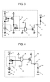
FIG. 3 is a circuit diagram illustrating yet another example of the output driver circuit according to the embodiment; -
FIG. 4 is a circuit diagram illustrating a further example of the output driver circuit according to the embodiment; and -
FIG. 5 is a circuit diagram illustrating a conventional output driver circuit. - The following will describe embodiments of the present invention with reference to the accompanying drawings.
-
FIG. 1 is a circuit diagram illustrating an output driver circuit of an embodiment. - An
output driver circuit 10 includes a constant-current circuit 11, a constant-currentmirror MOS transistor 12, aninput terminal 13, aselector circuit 14, and anNMOS transistor 15. - The gate of the
NMOS transistor 15 is connected to the output of theselector circuit 14, the source thereof is connected to agrounding terminal 2, and the drain thereof is connected to anoutput terminal 17. TheNMOS transistor 15 is an open-drain type output driver, theoutput terminal 17 being connected to asupply terminal 3 of a circuit in a subsequent stage through the intermediary of an external pull-up resistor 16. - The
selector circuit 14 is provided between the constant-currentmirror MOS transistor 12 and theNMOS transistor 15 so as to select either an output voltage of the constant-currentmirror MOS transistor 12 or a ground voltage VSS according to a voltage at theinput terminal 13. - The constant-current
mirror MOS transistor 12 receives a current generated in the constant-current circuit 11 connected to thegrounding terminal 2, and outputs a voltage for limiting the current between the source and the drain of theNMOS transistor 15. In other words, the constant-currentmirror MOS transistor 12 constitutes, together with theNMOS transistor 15, a current mirror circuit. - The operation of the
output driver circuit 10 of the present embodiment will now be described. - If the voltage of the
input terminal 13 is "L" level, then theselector circuit 14 outputs the ground voltage VSS. Hence, theNMOS transistor 15 turns off, placing theoutput terminal 17 of theoutput driver circuit 10 in a high impedance state. Hence, theoutput terminal 17 of theoutput driver circuit 10 is pulled up to a supply voltage VCC of a circuit in the subsequent stage, theoutput terminal 17 being connected to the input terminal of the circuit in the subsequent stage. In other words, theoutput driver circuit 10 outputs "H" level to theoutput terminal 17. - If the voltage of the
input terminal 13 is "H" level, then theselector circuit 14 outputs a gate voltage of the constant-currentmirror MOS transistor 12. This causes theNMOS transistor 15 to turn on, and a current determined on the basis of the supply voltage VCC and the resistance value of the pull-up resistor 16 will flow between the source and the drain. In other words, theoutput driver circuit 10 outputs "L" level to theoutput terminal 17. - It is assumed that the
output terminal 17 of theoutput driver circuit 10 and the supply voltage VCC of the circuit in the subsequent stage are short-circuited for some reason. If theNMOS transistor 15 is on, then the supply voltage VCC and the ground voltage VSS will be short-circuited, causing an overcurrent to flow between the source and the drain of theNMOS transistor 15. - A current limit value Ilimit of the current flowing between the source and the drain of the
NMOS transistor 15 is determined by a current Iconst generated in the constant-current circuit 11 and the current mirror ratio of the current mirror circuit. Thus, the current flowing between the source and the drain of theNMOS transistor 15 will be limited to the current limit value Ilimit regardless of the supply voltage VCC in the subsequent stage or the resistance value of the pull-up resistor 16. The current limit value Ilimit, which denotes a value for limiting an overcurrent, is set to a value that is sufficiently larger than the current that flow when theNMOS transistor 15 turns on at the time of the normal operation. - As described above, the output driver circuit of the embodiment is configured to control the gate voltage of the
NMOS transistor 15 by providing the constant-currentmirror MOS transistor 12 and theselector circuit 14, thus permitting the function for protecting theoutput terminal 17 from an overcurrent by using the simple circuit configuration. - As illustrated in
FIG. 2 , the constant-currentmirror MOS transistor 12 may be provided with an NMOS transistor and a fuse for adjusting current so as to make the current mirror ratio adjustable. Configuring the constant-currentmirror MOS transistor 12 in this manner makes it possible to restrain variations in the constant current Iconst and variations in the current mirror ratio. Hence, the accuracy of the current limit value Ilimit can be enhanced. - Further, although not shown, the constant-
current circuit 11 may be adjusted by, for example, fuse trimming, so as to restrain variations in the current limit value Ilimit. - Further, as illustrated in
FIG. 3 , the constant-currentmirror MOS transistor 12 may be configured to include a PMOS current mirror circuit that receives a current generated in the constant-current circuit 11 connected to thegrounding terminal 2. The PMOS current mirror circuit multiplies the current of the constant-current circuit 11 by the current mirror ratio and supplies the obtained current to a saturation-connected NMOS transistor. Configuring the constant-currentmirror MOS transistor 12 to provide two stages of the PMOS current mirror circuit and the NMOS current mirror circuit permits a reduced circuit area. Further, the current mirrors may be provided in any number of stages, and fuse trimming or the like may be used to make the current mirror ratio adjustable. - As illustrated in
FIG. 4 , in the case of a Pch open-drain type output driver circuit, the overcurrent protection function can be accomplished in the same manner by using the constant-currentmirror MOS transistor 12, aselector circuit 44, and anoutput MOS transistor 45. In this case, theoutput terminal 17 is connected to agrounding terminal 4 of the circuit in a subsequent stage through the intermediary of an external pull-up resistor 16. Further, the fuse trimming or the like may be used to add a function for restraining the variations in the current limit value Ilimit. -
- 10, 40
- output driver circuit
- 11
- constant-current circuit
- 12
- constant-current mirror MOS transistor
- 13, 53
- input terminal
- 14, 44
- selector circuit
- 15, 45
- output MOS transistor
- 17
- output terminal
- 51
- reference voltage circuit
- 52
- comparator
Claims (3)
- An output driver circuit with an open-drain output, comprising:a constant-current circuit which supplies a constant current;a constant-current mirror MOS transistor which generates a voltage based on the constant current;a selector circuit which receives the voltage based on the constant current that is generated by the constant-current mirror MOS transistor and a voltage of a first supply terminal and outputs one of the received voltages according to a signal supplied to an input terminal of the output driver circuit; andan output MOS transistor having a gate thereof connected to an output terminal of the selector circuit, a drain thereof connected to an output terminal of the output driver circuit, and a source thereof connected to the first supply terminal,wherein the constant-current mirror MOS transistor and the output MOS transistor constitute a current mirror circuit, anda current flowing between the source and the drain of the output MOS transistor is limited by a voltage based on the constant current.
- The output driver circuit according to claim 1, wherein
the current mirror circuit has a means for adjusting a current mirror ratio to adjust a current limit value of the output MOS transistor. - The output driver circuit according to claim 1, wherein
the constant-current circuit has a means for adjusting a current value so as to be capable of adjusting the current limit value of the output MOS transistor.
Applications Claiming Priority (2)
| Application Number | Priority Date | Filing Date | Title |
|---|---|---|---|
| JP2012103218A JP5806972B2 (en) | 2012-04-27 | 2012-04-27 | Output driver circuit |
| PCT/JP2013/058681 WO2013161483A1 (en) | 2012-04-27 | 2013-03-26 | Output driver circuit |
Publications (3)
| Publication Number | Publication Date |
|---|---|
| EP2846467A1 true EP2846467A1 (en) | 2015-03-11 |
| EP2846467A4 EP2846467A4 (en) | 2016-09-21 |
| EP2846467B1 EP2846467B1 (en) | 2019-03-06 |
Family
ID=49482817
Family Applications (1)
| Application Number | Title | Priority Date | Filing Date |
|---|---|---|---|
| EP13780640.2A Not-in-force EP2846467B1 (en) | 2012-04-27 | 2013-03-26 | Output driver circuit |
Country Status (7)
| Country | Link |
|---|---|
| US (1) | US10379565B2 (en) |
| EP (1) | EP2846467B1 (en) |
| JP (1) | JP5806972B2 (en) |
| KR (1) | KR101982904B1 (en) |
| CN (2) | CN111585552B (en) |
| TW (1) | TW201405276A (en) |
| WO (1) | WO2013161483A1 (en) |
Families Citing this family (4)
| Publication number | Priority date | Publication date | Assignee | Title |
|---|---|---|---|---|
| JPWO2016103620A1 (en) * | 2014-12-26 | 2017-10-05 | パナソニックIpマネジメント株式会社 | Display device and stand |
| US20160239091A1 (en) * | 2015-02-12 | 2016-08-18 | Qualcomm Incorporated | Controlled display of content on wearable displays |
| US9680474B1 (en) * | 2016-03-17 | 2017-06-13 | Xilinx, Inc. | System and method to reduce footprint and improve yield of fabric muxes in programmable logic devices |
| US9871514B1 (en) * | 2016-06-29 | 2018-01-16 | Texas Instruments Incorporated | Methods and apparatus for continuous current limiting for FETS in high inductive load systems |
Family Cites Families (19)
| Publication number | Priority date | Publication date | Assignee | Title |
|---|---|---|---|---|
| JPH05343967A (en) * | 1992-06-09 | 1993-12-24 | Toyota Autom Loom Works Ltd | Protection circuit |
| JPH0638363A (en) | 1992-07-20 | 1994-02-10 | Mitsubishi Electric Corp | Output driver circuit |
| JPH06113443A (en) * | 1992-09-25 | 1994-04-22 | Nec Kansai Ltd | Overcurrent detection protection circuit |
| US7740371B1 (en) * | 1998-03-19 | 2010-06-22 | Charles A. Lemaire | Method and apparatus for pulsed L.E.D. illumination for a camera |
| US6343024B1 (en) * | 2000-06-20 | 2002-01-29 | Stmicroelectronics, Inc. | Self-adjustable impedance line driver with hybrid |
| US7119611B2 (en) * | 2003-04-11 | 2006-10-10 | Vitesse Semiconductor Corporation | On-chip calibrated source termination for voltage mode driver and method of calibration thereof |
| JP4809064B2 (en) | 2006-01-13 | 2011-11-02 | ルネサスエレクトロニクス株式会社 | Current switch circuit |
| US7679876B2 (en) * | 2006-05-22 | 2010-03-16 | Mediatek Singapore Pte Ltd. | Current limiter system, circuit and method for limiting current |
| US7852057B2 (en) * | 2007-10-02 | 2010-12-14 | Mediatek Inc. | DC-DC converter |
| US8830644B2 (en) * | 2009-04-28 | 2014-09-09 | Semiconductor Components Industries, Llc | Method for providing over current protection and circuit |
| JP5533345B2 (en) * | 2009-12-25 | 2014-06-25 | ミツミ電機株式会社 | Current source circuit and delay circuit and oscillation circuit using the same |
| JP2011171854A (en) * | 2010-02-16 | 2011-09-01 | Canon Inc | Buffering circuit and amplifier circuit |
| WO2011111140A1 (en) * | 2010-03-10 | 2011-09-15 | パナソニック株式会社 | Variable gain amplifier |
| US8106710B2 (en) * | 2010-03-18 | 2012-01-31 | Analog Devices, Inc. | Apparatus and method for variable gain transconductance |
| TWI413361B (en) * | 2010-07-20 | 2013-10-21 | Ind Tech Res Inst | Current-mode amplifier |
| KR101419806B1 (en) * | 2010-11-19 | 2014-07-17 | 한국전자통신연구원 | Variable gain amplifier with fixed bandwidth |
| CN202085343U (en) * | 2011-01-25 | 2011-12-21 | 武汉光华芯科技有限公司 | High-performance LED constant-current driving circuit with wide power supply voltage range |
| JP5938852B2 (en) * | 2011-05-25 | 2016-06-22 | 富士電機株式会社 | Gate drive circuit of voltage controlled switching element |
| KR20150129155A (en) * | 2014-05-08 | 2015-11-19 | 에스케이하이닉스 주식회사 | Bias sampling apparatus, and cmos image sensor thereof |
-
2012
- 2012-04-27 JP JP2012103218A patent/JP5806972B2/en active Active
-
2013
- 2013-03-26 CN CN202010259966.2A patent/CN111585552B/en active Active
- 2013-03-26 WO PCT/JP2013/058681 patent/WO2013161483A1/en not_active Ceased
- 2013-03-26 EP EP13780640.2A patent/EP2846467B1/en not_active Not-in-force
- 2013-03-26 CN CN201380022125.8A patent/CN104247267A/en active Pending
- 2013-03-26 KR KR1020147029953A patent/KR101982904B1/en active Active
- 2013-04-10 TW TW102112690A patent/TW201405276A/en unknown
-
2014
- 2014-10-22 US US14/521,057 patent/US10379565B2/en active Active
Also Published As
| Publication number | Publication date |
|---|---|
| US20150035567A1 (en) | 2015-02-05 |
| JP5806972B2 (en) | 2015-11-10 |
| CN104247267A (en) | 2014-12-24 |
| JP2013232760A (en) | 2013-11-14 |
| CN111585552A (en) | 2020-08-25 |
| EP2846467B1 (en) | 2019-03-06 |
| KR20150015449A (en) | 2015-02-10 |
| TWI561956B (en) | 2016-12-11 |
| TW201405276A (en) | 2014-02-01 |
| EP2846467A4 (en) | 2016-09-21 |
| CN111585552B (en) | 2023-08-15 |
| KR101982904B1 (en) | 2019-05-27 |
| WO2013161483A1 (en) | 2013-10-31 |
| US10379565B2 (en) | 2019-08-13 |
Similar Documents
| Publication | Publication Date | Title |
|---|---|---|
| KR101435238B1 (en) | Voltage regulator | |
| US8547079B2 (en) | Voltage regulator capable of enabling overcurrent protection in a state in which an output current is large | |
| JP4589966B2 (en) | Power supply control device and semiconductor device | |
| US8957652B2 (en) | Output circuit | |
| US9692394B1 (en) | Programmable low power high-speed current steering logic (LPHCSL) driver and method of use | |
| US9748789B2 (en) | Charging/discharging control circuit, charging/discharging control device, and battery device | |
| US20160352319A1 (en) | Drive device | |
| JP5631918B2 (en) | Overcurrent protection circuit and power supply device | |
| EP4441893B1 (en) | Wide voltage gate driver using low gate oxide transistors | |
| US10379565B2 (en) | Output driver circuit | |
| KR101944540B1 (en) | Trimming circuit and semiconductor device | |
| CN105514942A (en) | protection method and protection device for electronic device | |
| JP2016206852A (en) | Current detection circuit | |
| US10274981B2 (en) | Voltage dropping apparatus, voltage switching apparatus, and internal voltage supply apparatus using the same | |
| US5889415A (en) | Internal voltage referenced output driver | |
| US7619864B1 (en) | Regulator short-circuit protection circuit and method | |
| JP2006352034A (en) | Fuse circuit and electronic circuit | |
| US7019581B1 (en) | Current sense circuit | |
| CN109245507B (en) | Overshoot-preventing protection circuit | |
| US6548994B2 (en) | Reference voltage generator tolerant to temperature variations | |
| US8817544B2 (en) | Readout circuit for non-volatile memory device | |
| JP6863571B2 (en) | Output driver circuit | |
| US6768618B1 (en) | Input gate protection circuit and method | |
| JP4594064B2 (en) | Surge current suppression circuit and DC power supply device | |
| KR101381376B1 (en) | Current limit switch |
Legal Events
| Date | Code | Title | Description |
|---|---|---|---|
| PUAI | Public reference made under article 153(3) epc to a published international application that has entered the european phase |
Free format text: ORIGINAL CODE: 0009012 |
|
| 17P | Request for examination filed |
Effective date: 20141127 |
|
| AK | Designated contracting states |
Kind code of ref document: A1 Designated state(s): AL AT BE BG CH CY CZ DE DK EE ES FI FR GB GR HR HU IE IS IT LI LT LU LV MC MK MT NL NO PL PT RO RS SE SI SK SM TR |
|
| AX | Request for extension of the european patent |
Extension state: BA ME |
|
| DAX | Request for extension of the european patent (deleted) | ||
| RAP1 | Party data changed (applicant data changed or rights of an application transferred) |
Owner name: SII SEMICONDUCTOR CORPORATION |
|
| RA4 | Supplementary search report drawn up and despatched (corrected) |
Effective date: 20160819 |
|
| RIC1 | Information provided on ipc code assigned before grant |
Ipc: H03K 19/003 20060101ALI20160812BHEP Ipc: H03K 19/0175 20060101AFI20160812BHEP Ipc: H02H 9/02 20060101ALI20160812BHEP Ipc: H03K 17/687 20060101ALI20160812BHEP Ipc: H03K 17/0812 20060101ALI20160812BHEP |
|
| STAA | Information on the status of an ep patent application or granted ep patent |
Free format text: STATUS: EXAMINATION IS IN PROGRESS |
|
| 17Q | First examination report despatched |
Effective date: 20180222 |
|
| RAP1 | Party data changed (applicant data changed or rights of an application transferred) |
Owner name: ABLIC INC. |
|
| GRAP | Despatch of communication of intention to grant a patent |
Free format text: ORIGINAL CODE: EPIDOSNIGR1 |
|
| STAA | Information on the status of an ep patent application or granted ep patent |
Free format text: STATUS: GRANT OF PATENT IS INTENDED |
|
| INTG | Intention to grant announced |
Effective date: 20181025 |
|
| GRAS | Grant fee paid |
Free format text: ORIGINAL CODE: EPIDOSNIGR3 |
|
| GRAA | (expected) grant |
Free format text: ORIGINAL CODE: 0009210 |
|
| STAA | Information on the status of an ep patent application or granted ep patent |
Free format text: STATUS: THE PATENT HAS BEEN GRANTED |
|
| AK | Designated contracting states |
Kind code of ref document: B1 Designated state(s): AL AT BE BG CH CY CZ DE DK EE ES FI FR GB GR HR HU IE IS IT LI LT LU LV MC MK MT NL NO PL PT RO RS SE SI SK SM TR |
|
| REG | Reference to a national code |
Ref country code: GB Ref legal event code: FG4D |
|
| REG | Reference to a national code |
Ref country code: CH Ref legal event code: EP Ref country code: AT Ref legal event code: REF Ref document number: 1105937 Country of ref document: AT Kind code of ref document: T Effective date: 20190315 |
|
| REG | Reference to a national code |
Ref country code: DE Ref legal event code: R096 Ref document number: 602013051890 Country of ref document: DE |
|
| REG | Reference to a national code |
Ref country code: IE Ref legal event code: FG4D |
|
| REG | Reference to a national code |
Ref country code: NL Ref legal event code: MP Effective date: 20190306 |
|
| REG | Reference to a national code |
Ref country code: LT Ref legal event code: MG4D |
|
| PG25 | Lapsed in a contracting state [announced via postgrant information from national office to epo] |
Ref country code: SE Free format text: LAPSE BECAUSE OF FAILURE TO SUBMIT A TRANSLATION OF THE DESCRIPTION OR TO PAY THE FEE WITHIN THE PRESCRIBED TIME-LIMIT Effective date: 20190306 Ref country code: FI Free format text: LAPSE BECAUSE OF FAILURE TO SUBMIT A TRANSLATION OF THE DESCRIPTION OR TO PAY THE FEE WITHIN THE PRESCRIBED TIME-LIMIT Effective date: 20190306 Ref country code: NO Free format text: LAPSE BECAUSE OF FAILURE TO SUBMIT A TRANSLATION OF THE DESCRIPTION OR TO PAY THE FEE WITHIN THE PRESCRIBED TIME-LIMIT Effective date: 20190606 Ref country code: LT Free format text: LAPSE BECAUSE OF FAILURE TO SUBMIT A TRANSLATION OF THE DESCRIPTION OR TO PAY THE FEE WITHIN THE PRESCRIBED TIME-LIMIT Effective date: 20190306 |
|
| PG25 | Lapsed in a contracting state [announced via postgrant information from national office to epo] |
Ref country code: GR Free format text: LAPSE BECAUSE OF FAILURE TO SUBMIT A TRANSLATION OF THE DESCRIPTION OR TO PAY THE FEE WITHIN THE PRESCRIBED TIME-LIMIT Effective date: 20190607 Ref country code: RS Free format text: LAPSE BECAUSE OF FAILURE TO SUBMIT A TRANSLATION OF THE DESCRIPTION OR TO PAY THE FEE WITHIN THE PRESCRIBED TIME-LIMIT Effective date: 20190306 Ref country code: HR Free format text: LAPSE BECAUSE OF FAILURE TO SUBMIT A TRANSLATION OF THE DESCRIPTION OR TO PAY THE FEE WITHIN THE PRESCRIBED TIME-LIMIT Effective date: 20190306 Ref country code: LV Free format text: LAPSE BECAUSE OF FAILURE TO SUBMIT A TRANSLATION OF THE DESCRIPTION OR TO PAY THE FEE WITHIN THE PRESCRIBED TIME-LIMIT Effective date: 20190306 Ref country code: NL Free format text: LAPSE BECAUSE OF FAILURE TO SUBMIT A TRANSLATION OF THE DESCRIPTION OR TO PAY THE FEE WITHIN THE PRESCRIBED TIME-LIMIT Effective date: 20190306 Ref country code: BG Free format text: LAPSE BECAUSE OF FAILURE TO SUBMIT A TRANSLATION OF THE DESCRIPTION OR TO PAY THE FEE WITHIN THE PRESCRIBED TIME-LIMIT Effective date: 20190606 |
|
| REG | Reference to a national code |
Ref country code: AT Ref legal event code: MK05 Ref document number: 1105937 Country of ref document: AT Kind code of ref document: T Effective date: 20190306 |
|
| PG25 | Lapsed in a contracting state [announced via postgrant information from national office to epo] |
Ref country code: IT Free format text: LAPSE BECAUSE OF FAILURE TO SUBMIT A TRANSLATION OF THE DESCRIPTION OR TO PAY THE FEE WITHIN THE PRESCRIBED TIME-LIMIT Effective date: 20190306 Ref country code: ES Free format text: LAPSE BECAUSE OF FAILURE TO SUBMIT A TRANSLATION OF THE DESCRIPTION OR TO PAY THE FEE WITHIN THE PRESCRIBED TIME-LIMIT Effective date: 20190306 Ref country code: CZ Free format text: LAPSE BECAUSE OF FAILURE TO SUBMIT A TRANSLATION OF THE DESCRIPTION OR TO PAY THE FEE WITHIN THE PRESCRIBED TIME-LIMIT Effective date: 20190306 Ref country code: RO Free format text: LAPSE BECAUSE OF FAILURE TO SUBMIT A TRANSLATION OF THE DESCRIPTION OR TO PAY THE FEE WITHIN THE PRESCRIBED TIME-LIMIT Effective date: 20190306 Ref country code: EE Free format text: LAPSE BECAUSE OF FAILURE TO SUBMIT A TRANSLATION OF THE DESCRIPTION OR TO PAY THE FEE WITHIN THE PRESCRIBED TIME-LIMIT Effective date: 20190306 Ref country code: SK Free format text: LAPSE BECAUSE OF FAILURE TO SUBMIT A TRANSLATION OF THE DESCRIPTION OR TO PAY THE FEE WITHIN THE PRESCRIBED TIME-LIMIT Effective date: 20190306 Ref country code: PT Free format text: LAPSE BECAUSE OF FAILURE TO SUBMIT A TRANSLATION OF THE DESCRIPTION OR TO PAY THE FEE WITHIN THE PRESCRIBED TIME-LIMIT Effective date: 20190706 Ref country code: AL Free format text: LAPSE BECAUSE OF FAILURE TO SUBMIT A TRANSLATION OF THE DESCRIPTION OR TO PAY THE FEE WITHIN THE PRESCRIBED TIME-LIMIT Effective date: 20190306 |
|
| REG | Reference to a national code |
Ref country code: CH Ref legal event code: PL |
|
| PG25 | Lapsed in a contracting state [announced via postgrant information from national office to epo] |
Ref country code: PL Free format text: LAPSE BECAUSE OF FAILURE TO SUBMIT A TRANSLATION OF THE DESCRIPTION OR TO PAY THE FEE WITHIN THE PRESCRIBED TIME-LIMIT Effective date: 20190306 Ref country code: LU Free format text: LAPSE BECAUSE OF NON-PAYMENT OF DUE FEES Effective date: 20190326 Ref country code: SM Free format text: LAPSE BECAUSE OF FAILURE TO SUBMIT A TRANSLATION OF THE DESCRIPTION OR TO PAY THE FEE WITHIN THE PRESCRIBED TIME-LIMIT Effective date: 20190306 |
|
| REG | Reference to a national code |
Ref country code: BE Ref legal event code: MM Effective date: 20190331 |
|
| REG | Reference to a national code |
Ref country code: DE Ref legal event code: R097 Ref document number: 602013051890 Country of ref document: DE |
|
| PG25 | Lapsed in a contracting state [announced via postgrant information from national office to epo] |
Ref country code: IS Free format text: LAPSE BECAUSE OF FAILURE TO SUBMIT A TRANSLATION OF THE DESCRIPTION OR TO PAY THE FEE WITHIN THE PRESCRIBED TIME-LIMIT Effective date: 20190706 Ref country code: AT Free format text: LAPSE BECAUSE OF FAILURE TO SUBMIT A TRANSLATION OF THE DESCRIPTION OR TO PAY THE FEE WITHIN THE PRESCRIBED TIME-LIMIT Effective date: 20190306 |
|
| PLBE | No opposition filed within time limit |
Free format text: ORIGINAL CODE: 0009261 |
|
| STAA | Information on the status of an ep patent application or granted ep patent |
Free format text: STATUS: NO OPPOSITION FILED WITHIN TIME LIMIT |
|
| PG25 | Lapsed in a contracting state [announced via postgrant information from national office to epo] |
Ref country code: CH Free format text: LAPSE BECAUSE OF NON-PAYMENT OF DUE FEES Effective date: 20190331 Ref country code: MC Free format text: LAPSE BECAUSE OF FAILURE TO SUBMIT A TRANSLATION OF THE DESCRIPTION OR TO PAY THE FEE WITHIN THE PRESCRIBED TIME-LIMIT Effective date: 20190306 Ref country code: LI Free format text: LAPSE BECAUSE OF NON-PAYMENT OF DUE FEES Effective date: 20190331 Ref country code: IE Free format text: LAPSE BECAUSE OF NON-PAYMENT OF DUE FEES Effective date: 20190326 Ref country code: DK Free format text: LAPSE BECAUSE OF FAILURE TO SUBMIT A TRANSLATION OF THE DESCRIPTION OR TO PAY THE FEE WITHIN THE PRESCRIBED TIME-LIMIT Effective date: 20190306 |
|
| 26N | No opposition filed |
Effective date: 20191209 |
|
| GBPC | Gb: european patent ceased through non-payment of renewal fee |
Effective date: 20190606 |
|
| PG25 | Lapsed in a contracting state [announced via postgrant information from national office to epo] |
Ref country code: SI Free format text: LAPSE BECAUSE OF FAILURE TO SUBMIT A TRANSLATION OF THE DESCRIPTION OR TO PAY THE FEE WITHIN THE PRESCRIBED TIME-LIMIT Effective date: 20190306 Ref country code: BE Free format text: LAPSE BECAUSE OF NON-PAYMENT OF DUE FEES Effective date: 20190331 |
|
| PG25 | Lapsed in a contracting state [announced via postgrant information from national office to epo] |
Ref country code: TR Free format text: LAPSE BECAUSE OF FAILURE TO SUBMIT A TRANSLATION OF THE DESCRIPTION OR TO PAY THE FEE WITHIN THE PRESCRIBED TIME-LIMIT Effective date: 20190306 |
|
| PG25 | Lapsed in a contracting state [announced via postgrant information from national office to epo] |
Ref country code: GB Free format text: LAPSE BECAUSE OF NON-PAYMENT OF DUE FEES Effective date: 20190606 |
|
| PG25 | Lapsed in a contracting state [announced via postgrant information from national office to epo] |
Ref country code: MT Free format text: LAPSE BECAUSE OF NON-PAYMENT OF DUE FEES Effective date: 20190326 |
|
| PG25 | Lapsed in a contracting state [announced via postgrant information from national office to epo] |
Ref country code: CY Free format text: LAPSE BECAUSE OF FAILURE TO SUBMIT A TRANSLATION OF THE DESCRIPTION OR TO PAY THE FEE WITHIN THE PRESCRIBED TIME-LIMIT Effective date: 20190306 |
|
| PG25 | Lapsed in a contracting state [announced via postgrant information from national office to epo] |
Ref country code: HU Free format text: LAPSE BECAUSE OF FAILURE TO SUBMIT A TRANSLATION OF THE DESCRIPTION OR TO PAY THE FEE WITHIN THE PRESCRIBED TIME-LIMIT; INVALID AB INITIO Effective date: 20130326 |
|
| PG25 | Lapsed in a contracting state [announced via postgrant information from national office to epo] |
Ref country code: MK Free format text: LAPSE BECAUSE OF FAILURE TO SUBMIT A TRANSLATION OF THE DESCRIPTION OR TO PAY THE FEE WITHIN THE PRESCRIBED TIME-LIMIT Effective date: 20190306 |
|
| PGFP | Annual fee paid to national office [announced via postgrant information from national office to epo] |
Ref country code: FR Payment date: 20230324 Year of fee payment: 11 |
|
| PGFP | Annual fee paid to national office [announced via postgrant information from national office to epo] |
Ref country code: DE Payment date: 20230321 Year of fee payment: 11 |
|
| REG | Reference to a national code |
Ref country code: DE Ref legal event code: R081 Ref document number: 602013051890 Country of ref document: DE Owner name: ABLIC INC., MIYOTA-MACHI, JP Free format text: FORMER OWNER: ABLIC INC., CHIBA-SHI, JP |
|
| P01 | Opt-out of the competence of the unified patent court (upc) registered |
Effective date: 20230530 |
|
| REG | Reference to a national code |
Ref country code: DE Ref legal event code: R119 Ref document number: 602013051890 Country of ref document: DE |
|
| PG25 | Lapsed in a contracting state [announced via postgrant information from national office to epo] |
Ref country code: DE Free format text: LAPSE BECAUSE OF NON-PAYMENT OF DUE FEES Effective date: 20241001 |
|
| PG25 | Lapsed in a contracting state [announced via postgrant information from national office to epo] |
Ref country code: FR Free format text: LAPSE BECAUSE OF NON-PAYMENT OF DUE FEES Effective date: 20240331 |
|
| PG25 | Lapsed in a contracting state [announced via postgrant information from national office to epo] |
Ref country code: FR Free format text: LAPSE BECAUSE OF NON-PAYMENT OF DUE FEES Effective date: 20240331 Ref country code: DE Free format text: LAPSE BECAUSE OF NON-PAYMENT OF DUE FEES Effective date: 20241001 |