EP2845208B1 - Kupfer-flachwicklung zur erzeugung magnetischer felder in elektrischen energiewandlern mit hohen füllfaktoren - Google Patents
Kupfer-flachwicklung zur erzeugung magnetischer felder in elektrischen energiewandlern mit hohen füllfaktoren Download PDFInfo
- Publication number
- EP2845208B1 EP2845208B1 EP13716985.0A EP13716985A EP2845208B1 EP 2845208 B1 EP2845208 B1 EP 2845208B1 EP 13716985 A EP13716985 A EP 13716985A EP 2845208 B1 EP2845208 B1 EP 2845208B1
- Authority
- EP
- European Patent Office
- Prior art keywords
- copper
- copper strip
- repeating pattern
- winding
- strip
- Prior art date
- Legal status (The legal status is an assumption and is not a legal conclusion. Google has not performed a legal analysis and makes no representation as to the accuracy of the status listed.)
- Active
Links
- RYGMFSIKBFXOCR-UHFFFAOYSA-N Copper Chemical compound [Cu] RYGMFSIKBFXOCR-UHFFFAOYSA-N 0.000 title claims description 73
- 229910052802 copper Inorganic materials 0.000 title claims description 71
- 239000010949 copper Substances 0.000 title claims description 71
- 238000004804 winding Methods 0.000 title claims description 31
- 230000005291 magnetic effect Effects 0.000 title description 13
- 238000004519 manufacturing process Methods 0.000 claims description 13
- 238000000034 method Methods 0.000 claims description 11
- 239000012777 electrically insulating material Substances 0.000 claims description 8
- 238000000576 coating method Methods 0.000 claims description 7
- 239000011248 coating agent Substances 0.000 claims description 6
- 238000000137 annealing Methods 0.000 claims description 5
- 238000005452 bending Methods 0.000 claims description 3
- 238000005520 cutting process Methods 0.000 claims description 3
- 230000003628 erosive effect Effects 0.000 claims description 3
- 238000003698 laser cutting Methods 0.000 claims description 3
- 239000007921 spray Substances 0.000 claims description 2
- 238000004080 punching Methods 0.000 claims 1
- 239000004020 conductor Substances 0.000 description 12
- 239000011162 core material Substances 0.000 description 4
- 230000001939 inductive effect Effects 0.000 description 3
- 238000007654 immersion Methods 0.000 description 2
- 230000006698 induction Effects 0.000 description 2
- 239000000696 magnetic material Substances 0.000 description 2
- 239000000463 material Substances 0.000 description 2
- 230000010287 polarization Effects 0.000 description 2
- XLYOFNOQVPJJNP-UHFFFAOYSA-N water Substances O XLYOFNOQVPJJNP-UHFFFAOYSA-N 0.000 description 2
- 238000005266 casting Methods 0.000 description 1
- 238000005516 engineering process Methods 0.000 description 1
- 239000003302 ferromagnetic material Substances 0.000 description 1
- 230000004907 flux Effects 0.000 description 1
- 238000009413 insulation Methods 0.000 description 1
- 238000003754 machining Methods 0.000 description 1
- 230000035699 permeability Effects 0.000 description 1
- 238000007493 shaping process Methods 0.000 description 1
- 238000005482 strain hardening Methods 0.000 description 1
- 238000007669 thermal treatment Methods 0.000 description 1
Images



Classifications
-
- H—ELECTRICITY
- H01—ELECTRIC ELEMENTS
- H01F—MAGNETS; INDUCTANCES; TRANSFORMERS; SELECTION OF MATERIALS FOR THEIR MAGNETIC PROPERTIES
- H01F27/00—Details of transformers or inductances, in general
- H01F27/28—Coils; Windings; Conductive connections
- H01F27/2847—Sheets; Strips
-
- H—ELECTRICITY
- H01—ELECTRIC ELEMENTS
- H01F—MAGNETS; INDUCTANCES; TRANSFORMERS; SELECTION OF MATERIALS FOR THEIR MAGNETIC PROPERTIES
- H01F41/00—Apparatus or processes specially adapted for manufacturing or assembling magnets, inductances or transformers; Apparatus or processes specially adapted for manufacturing materials characterised by their magnetic properties
- H01F41/02—Apparatus or processes specially adapted for manufacturing or assembling magnets, inductances or transformers; Apparatus or processes specially adapted for manufacturing materials characterised by their magnetic properties for manufacturing cores, coils, or magnets
- H01F41/04—Apparatus or processes specially adapted for manufacturing or assembling magnets, inductances or transformers; Apparatus or processes specially adapted for manufacturing materials characterised by their magnetic properties for manufacturing cores, coils, or magnets for manufacturing coils
- H01F41/06—Coil winding
- H01F41/061—Winding flat conductive wires or sheets
-
- H—ELECTRICITY
- H02—GENERATION; CONVERSION OR DISTRIBUTION OF ELECTRIC POWER
- H02K—DYNAMO-ELECTRIC MACHINES
- H02K15/00—Processes or apparatus specially adapted for manufacturing, assembling, maintaining or repairing of dynamo-electric machines
- H02K15/04—Processes or apparatus specially adapted for manufacturing, assembling, maintaining or repairing of dynamo-electric machines of windings prior to their mounting into the machines
- H02K15/043—Processes or apparatus specially adapted for manufacturing, assembling, maintaining or repairing of dynamo-electric machines of windings prior to their mounting into the machines winding flat conductive wires or sheets
- H02K15/0431—Concentrated windings
-
- H—ELECTRICITY
- H01—ELECTRIC ELEMENTS
- H01F—MAGNETS; INDUCTANCES; TRANSFORMERS; SELECTION OF MATERIALS FOR THEIR MAGNETIC PROPERTIES
- H01F27/00—Details of transformers or inductances, in general
- H01F27/28—Coils; Windings; Conductive connections
- H01F27/2847—Sheets; Strips
- H01F2027/2861—Coil formed by folding a blank
Definitions
- the present invention relates to a method for producing a copper flat winding.
- Coil windings for generating magnetic fields in energy converters, in particular electromagnetic actuators and rotating electrical machines, are today mostly made with enamelled copper wire.
- This enamelled wire usually has a round cross-section.
- a coil former for example a magnetic pot, stator or rotor tooth with a soft magnetic core material
- the soft magnetic core material is one of the ferromagnetic materials that can be easily magnetized in a magnetic field. This magnetic polarization can be generated, for example, by an electric current in a current-carrying coil or by the presence of a permanent magnet.
- copper fill factor denotes the amount of electrical conductors, including their insulation layer, that is introduced into the available winding space. A round wire therefore always encloses spaces that are not electrically effective.
- the copper fill factor can be further increased by using special profile wires, for example wires with a square cross-section. Most recently in the scientific Coils cast in the vicinity are discussed, which lead to a significantly higher copper fill factor (up to approx. 70%) with a rectangular cross section (see Fig. 2 ).
- DE 17 64 087 A1 discloses a method of making folded windings for electrical induction devices.
- EP 0 662 699 A1 relates to a charging system which comprises an inductive charging coupler which can be connected to an energy source and which comprises an inductive charging socket into which the inductive charging coupler can be inserted.
- DE 100 58 874 A1 discloses a meandering conductor formed from a metallic band into a self-supporting coil.
- US 2005/122200 A1 discloses a high current, low profile inductor comprising an induction coil surrounded by a magnetic material to form an inductor body.
- the present invention relates to a method for producing a flat copper winding according to claim 1.
- the process technology required can be based on particularly simple and inexpensive processes.
- the copper strip can have a rectangular cross section. This has the advantage over a cast flat winding that the manufacturing process is simpler and cheaper.
- the repeating pattern is produced by a stamping process, laser cutting, eroding or by water jet cutting. This enables the repeating pattern to be produced in a simple and inexpensive manner.
- the repeating pattern can have a cuboid, cylindrical, polygonal, oval, round or similar shape, the shape of the repeating pattern depending on the shape of the coil carrier, onto which the copper flat winding is later placed to produce an energy converter.
- the thickness of the copper strip can correspond to a first dimension of a conductor cross-section and the width of the copper strip can result from a second dimension of the conductor cross-section and from the dimensions of a coil carrier.
- the conductor cross-section can be tailored to the needs of the user can be selected to produce a desired energy converter.
- the second dimension of the conductor cross section can be formed using the repeating pattern. By generating the repeating pattern, the dimensions of the coil support can be separated from the width of the copper strip, so that the remaining part of the copper strip can correspond to the second dimension of the conductor cross section.
- the width of the copper tape can correspond to several partial strips. This means that several copper flat windings can be produced from one copper strip in one process step.
- the spiral body is annealed after cold working. Sufficient electrical conductivity can be restored by the annealing treatment.
- the spiral-shaped body is coated with an electrically insulating material after the annealing treatment.
- the punched or cut edges can advantageously also be isolated in the manufacturing process.
- the electrically insulating coating of the copper flat winding can advantageously be carried out by an immersion bath or by a spray treatment. As a result, an electrically insulating coating of the flat copper winding can be implemented in a particularly simple and inexpensive manner.
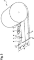
- Fig. 3 shows a copper strip 2.
- the copper strip 2 is provided to a copper flat winding 1 (see Fig. 7 ) to manufacture.
- the copper strip 2 can be seen rolled up into a roll and has a rectangular cross section.
- the copper strip 2 is coated with an electrically insulating material (in Fig. 1 is not shown). This means that it is not necessary to coat the finished copper flat winding with an electrically insulating material.
- the copper strip 2 has a thickness a, which corresponds to a first dimension of a conductor cross section.
- the conductor cross section is in this way by the user selected in order to produce a desired energy converter with the aid of the copper flat winding 1 produced and a coil carrier (not shown).
- the width b of the copper strip 2 results from a second dimension d (see Figure 4 ) of the conductor cross section, as well as the dimensions of a coil carrier (not shown).
- the second dimension d of the conductor cross section is formed over the repeating pattern 4.
- the dimensions of the coil carrier are separated from the width b of the copper strip 2, so that the remaining part of the copper strip 2 corresponds to the second dimension d of the conductor cross section.
- the width b of the copper strip 2 consists of several sections bn.
- the width b corresponds to exactly 3 sections bn.
- the copper strip 2 is divided into three partial strips 3 during the first production process in this example.
- the width b of the copper strip b corresponds exactly to the width b of the flat copper winding 1 and thus has no sections bn, or that there are only two sections bn or more than three sections bn.
- the dimension of the coil carrier is required in order to produce a repeating pattern 4 in the copper strip 2 and, if necessary, in each partial strip 3.
- the repeating pattern 4 is a cuboid recess, but it is also possible for the repeating pattern 4 to have another shape, such as, for example, a polygon, a circle, an oval, a rhombus or another shape.
- the repeating pattern 4 corresponds to the shape of a coil carrier, on which the finished copper flat winding 1 is placed in order to produce an energy converter.
- the copper strip 2 is also divided into the corresponding number of partial strips 3 if necessary.
- Fig. 3 it can be seen that three partial strips 3 are produced from the copper strip 2, a repeating pattern 4 having already been generated on only one partial strip 3. A repeating pattern 4 is also generated in the other partial strips 3; this is shown in FIG Fig. 3 not shown.
- the repeating pattern 4 is produced by a continuous stamping process, laser cutting, eroding, or water jet cutting. In this way, simple, inexpensive manufacturing processes can be used to produce the repeating pattern 4.
- Fig. 4 a top view of a copper strip 2 with a repeating pattern 4 is shown.
- the copper strip has the width b and has a repeating pattern 4 with a cuboid recess, the cuboid recess representing a cyclically repeating geometry.
- Cold forming of the copper strip 2 for example by folding at the intended forming edges C highlighted with the dashed lines, forms a spiral body 6 by alternate bending.
- the cold forming manufacturing process is in Fig. 5 shown.
- the copper strip 2 is placed in a device 7.
- the repeating pattern 4 of the copper strip 2 is then formed on the forming edge C with the aid of a tool 5.
- the tool 5 can be, for example, a tooth of a wheel or a stamp.
- the tool 5 acts on the forming edge C with a force F.
- the changing pattern 4 of the copper strip 2 is bent over at a forming edge C and transported after each bending of a forming edge C to the next forming edge C, so that it is alternately bent from the copper strip 2 a spiral body 6 is produced at the forming edges C of the repeating pattern 4.
- the spiral body 6 is compressed in a further device (not shown) with a force F 2 , so that the turns of the spiral body 6 lie on one another. This creates a fully processed flat copper winding 1.
- FIG. 6 An embodiment of the invention is in Fig. 6 shown.
- the copper strip 2 is not coated with an electrically insulating material in this embodiment.
- the copper strip 2 it would be possible for the copper strip 2 to be coated with an electrically insulating material, but because of the necessary thermal treatment, the electrically insulating material would not be able to withstand the temperatures, so that a new coating is necessary.
- the spiral body 6 is immersed in an immersion bath 8 in order to coat the spiral body 6 with an electrically insulating material. This also isolates the edges that arise during the manufacturing processes. After the coating, the spiral body 6 is compressed in a further device (not shown) with a force F 2 , so that the turns of the spiral body 6 lie on one another. This creates a fully processed flat copper winding 1.
- a finished processed copper flat winding 1 is in Fig. 7 shown. It can be seen from the layers lying one above the other that the copper flat winding 1 has been produced from a copper strip 2 with the thickness a.
- the copper flat winding 1 has a width b.
- the layers one above the other represent copper webs that are insulated from one another.
- An energy converter (not shown) is produced in such a way that the finished copper flat winding 1 is plugged onto a coil carrier as a coil package.
- the connection tabs are then contacted.
- the coil carrier consists of a soft magnetic core material and is, for example, a magnetic pot, stator tooth or rotor tooth.
Landscapes
- Engineering & Computer Science (AREA)
- Power Engineering (AREA)
- Manufacturing & Machinery (AREA)
- Manufacture Of Motors, Generators (AREA)
- Windings For Motors And Generators (AREA)
- Manufacturing Cores, Coils, And Magnets (AREA)
- Coils Of Transformers For General Uses (AREA)
Description
- Die vorliegende Erfindung betrifft ein Verfahren zur Herstellung einer Kupfer-Flachwicklung.
- Spulenwicklungen zur Erzeugung von Magnetfeldern in Energiewandlern, insbesondere elektromagnetische Aktoren und rotierende elektrische Maschinen, werden heute zumeist mit Kupfer-Lackdraht ausgeführt. Dieser Lackdraht besitzt in der Regel einen runden Querschnitt. Hieraus ergibt sich bei der Bewicklung eines Spulenträgers, beispielsweise ein Magnettopf, Stator- oder Rotorzahn mit einem weichmagnetischen Kernmaterial, ein sogenannter Kupferfüllfaktor, der je nach Wicklung z.B. im Bereich von 40-55% liegt (siehe
Fig. 1 ). Das weichmagnetische Kernmaterial gehört zu den ferromagnetischen Materialien, die sich in einem Magnetfeld leicht magnetisieren lassen. Diese magnetische Polarisation kann beispielsweise durch einen elektrischen Strom in einer stromdurchflossenen Spule oder durch Anwesenheit eines Permanentmagneten erzeugt werden. Die Polarisation führt in allen weichmagnetischen Werkstoffen zu einer vielfach höheren magnetischen Flussdichte als das von außen wirkende magnetische Feld in Luft erzeugt. Dadurch kann ein weichmagnetisches Kernmaterial ein äußeres Magnetfeld um die Werkstoffpermeabilität verstärken. Der Begriff Kupferfüllfaktor bezeichnet hierbei, die in den zur Verfügung stehenden Wickelraum eingebrachte Menge an elektrischen Leitern einschließlich deren Isolationsschicht. Ein runder Draht schließt somit immer Räume ein, die nicht elektrisch wirksam sind. Durch spezielle Profildrähte, beispielsweise Drähte mit quadratischem Querschnitt, kann der Kupferfüllfaktor weiter gesteigert werden. Jüngst werden im wissenschaftlichen Umfeld gegossene Spulen diskutiert, welche bei rechteckigem Querschnitt zu einem deutlich höheren Kupferfüllfaktor (bis ca. 70%) führen (sieheFig. 2 ). - Der Prozess des Gießens von derartigen Spulen sowie der Beschichtung ist vergleichsweise zeit-, material-, und somit kostenintensiv.
-
DE 17 64 087 A1 offenbart ein Verfahren zum Herstellen von Faltwicklungen für elektrische Induktionsgeräte. -
EP 0 662 699 A1 betrifft ein Ladesystem, das einen Induktivladekoppler umfasst, der an eine Energiequelle anschließbar ist, und das eine Induktivladedose umfasst, in die der Induktivladekoppler einführbar ist. -
DE 100 58 874 A1 offenbart einen Mäanderförmigen Leiter, geformt aus einem metallischen Band zu einer selbsttragenden Spule. -
US 2005/122200 A1 offenbart einen Induktor mit hohem Strom und niedrigem Profil umfassend eine Induktionsspule, die von einem magnetischen Material umgeben ist, um einen Induktorkörper zu bilden. - Gegenstand der vorliegenden Erfindung ist ein Verfahren zur Herstellung einer Kupferflachwicklung gemäss Anspruch 1.
- Hierdurch kann durch einfache Fertigungsprozesse gegenüber dem Stand der Technik ein hoher Kupferfüllfaktor erreicht werden. Dabei kann die erforderliche Prozesstechnologie auf besonders einfachen und preisgünstigen Verfahren beruhen. Das Kupferband kann dabei einen rechteckigen Querschnitt aufweisen. Dies hat gegenüber einer gegossenen Flachwicklung den Vorteil, dass der Fertigungsprozess einfacher und kostengünstiger ist.
- Erfindungsgemäss wird das sich wiederholende Muster durch ein Stanzverfahren, Laserschneiden, Erodieren oder durch Wasserstrahlschneiden erzeugt. Dies ermöglicht es, dass das sich wiederholende Muster auf einfache und kostengünstige Weise hergestellt wird. Dabei kann das sich wiederholende Muster eine quaderförmige, zylindrische, mehreckige, ovale, runde oder ähnliche Form aufweisen, wobei die Form des sich wiederholenden Musters sich nach der Form des Spulenträgers richtet, auf welche die Kupferflachwicklung später draufgesteckt wird, um einen Energiewandler herzustellen.
- Die Dicke des Kupferbandes kann einem ersten Maß eines Leiterquerschnitts entsprechen und die Breite des Kupferbandes kann sich aus einem zweiten Maß des Leiterquerschnitts und sich aus den Abmessungen eines Spulenträgers ergeben. Dabei kann der Leiterquerschnitt dem Wunsch des Benutzers entsprechend ausgewählt werden, um einen gewünschten Energiewandler herzustellen. Das zweite Maß des Leiterquerschnitts kann dabei über das sich wiederholende Muster gebildet werden. Durch das Erzeugen des sich wiederholenden Musters kann von der Breite des Kupferbandes die Abmaße des Spulenträgers herausgetrennt werden, so dass der übrig bleibende Teil des Kupferbandes dem zweiten Maß des Leiterquerschnitts entsprechen kann. Das Kupferband kann in der Breite mehreren Teilstreifen entsprechen. Dadurch kann in einem Prozessschritt aus einem Kupferband mehrere Kupfer-Flachwicklungen hergestellt werden.
- Erfindungsgemäss wird der spiralförmige Körper nach der Kaltverformung glühbehandelt. Durch die Glühbehandlung kann eine ausreichende elektrische Leitfähigkeit wieder hergestellt werden.
- Erfindungsgemäss wird der spiralförmige Körper nach der Glühbehandlung mit einem elektrisch isolierenden Stoff beschichtet. Dadurch können vorteilhafterweise auch die Stanz- oder Schnittkanten bei dem Herstellungsprozess mit isoliert werden.
- Vorteilhafterweise kann die elektrisch isolierende Beschichtung der Kupfer-Flachwicklung durch ein Tauchbad oder durch eine Sprühbehandlung erfolgen. Dadurch kann auf eine besonders einfache und kostengünstige Weise eine elektrisch isolierende Beschichtung der Kupfer-Flachwicklung verwirklicht werden.
- Hinsichtlich weiterer bevorzugter Merkmale und Vorteile des erfindungsgemäßen Gegenstands wird hiermit explizit auf die Erläuterungen im Zusammenhang mit dem erfindungsgemäßen Verfahren zur Herstellung einer Kupfer-Flachwicklung sowie auf die Beispiele verwiesen.
- Weitere Vorteile und vorteilhafte Ausgestaltungen der erfindungsgemäßen Gegenstände werden durch die Zeichnung und die Beispiele veranschaulicht und in der nachfolgenden Beschreibung erläutert. Dabei ist zu beachten, dass die Zeichnung und die Beispiele nur beschreibenden Charakter haben und nicht dazu gedacht sind, die Erfindung in irgendeiner Form einzuschränken. Es zeigt
- Fig. 1
- eine Ansicht eines Kupferfüllfaktor aus einem Ausschnitt eines Querschnitts eines Energiewandlers mit rundem Kupfer-Lackdraht,
- Fig. 2
- eine Ansicht eines Kupferfüllfaktor aus einem Ausschnitt eines Querschnitts eines Energiewandlers mit einer gegossenen Spule mit einem rechteckigen Querschnitt,
- Fig. 3
- eine Ansicht eines Kupferbandes, welches zur Herstellung der Kupfer-Flachwicklung verwendet wird,
- Fig. 4
- eine Draufsicht auf einen Teilstreifen eines Kupferbandes mit einem sich wiederholenden Musters,
- Fig. 5
- eine schematische Ansicht eines Umformungsprozesses, bei dem eine Kupfer-Flachwicklung aus einem Kupferband hergestellt wird,
- Fig. 6
- eine schematische Ansicht eines Beschichtungsverfahrens der Kupfer-Flachwicklung vor dem letzten Kaltumformungsprozess,
- Fig. 7
- eine isometrische Ansicht einer Kupfer-Flachwicklung.
- 1.
- Herstellung einer Kupferflachwicklung
-
Fig. 3 zeigt ein Kupferband 2. Das Kupferband 2 wird bereitgestellt, um eine Kupfer-Flachwicklung 1 (sieheFig. 7 ) herzustellen. Wie inFig. 3 erkennbar ist das Kupferband 2 zu einer Rolle aufgerollt und hat einen rechteckigen Querschnitt. , In diesem Beispiel, das nicht Teil der Erfindung ist, ist das Kupferband 2 mit einem elektrisch isolierenden Stoff beschichtet ist (inFig. 1 ist nicht dargestellt). Dadurch ist es nicht notwendig die fertig prozessierte Kupfer-Flachwicklung mit einem elektrisch isolierenden Stoff zu beschichten. - Das Kupferband 2 weist eine Dicke a auf, welche einem ersten Maß eines Leiterquerschnitts entspricht. Der Leiterquerschnitt wird dabei derart vom Benutzer ausgewählt um mit Hilfe der hergestellten Kupfer-Flachwicklung 1 und einem Spulenträger (nicht dargestellt) einen gewünschten Energiewandler herzustellen.
- Weiterhin ist in
Fig. 3 erkennbar, dass die Breite b des Kupferbandes 2 sich aus einem zweitem Maß d (sieheFigur 4 ) des Leiterquerschnitts, sowie der Abmessungen eines Spulenträgers (nicht dargestellt) ergibt. Das zweite Maß d des Leiterquerschnitts wird dabei über das sich wiederholende Muster 4 gebildet. Durch das Erzeugen des sich wiederholenden Musters 4 wird von der Breite b des Kupferbandes 2 die Abmaße des Spulenträgers herausgetrennt, so dass der übrig bleibende Teil des Kupferbandes2 dem zweiten Maß d des Leiterquerschnitts entspricht. - In dem in
Fig. 3 dargestellten Beispiel ist erkennbar, dass die Breite b des Kupferbandes 2 mehreren Teilbreiten bn besteht. In diesem Beispiel entspricht die Breite b genau 3 Teilbreiten bn. Dies bedeutet, dass das Kupferband 2 während des ersten Fertigungsprozesses in diesem Beispiel in drei Teilstreifen 3 aufgeteilt wird. Es ist jedoch auch möglich, dass die Breite b des Kupferbandes b genau der Breite b der Kupferflachwicklung 1 entspricht und somit keine Teilbreiten bn aufweist, oder dass nur zwei Teilbreiten bn oder mehr als drei Teilbreiten bn vorhanden sind. - Die Abmessung des Spulenträgers wird benötigt, um ein sich wiederholendes Muster 4 in das Kupferband 2 und falls nötig in jedem Teilstreifen 3 zu erzeugen. In diesem Beispiel ist das sich wiederholende Muster 4 eine quaderförmige Aussparung, jedoch ist es auch möglich, dass das sich wiederholende Muster 4 eine andere Form, wie beispielsweise ein Mehreck, ein Kreis, ein Oval, eine Raute oder eine andere Form aufweist. Das sich wiederholende Muster 4 entspricht der Form eines Spulenträgers, auf dem die fertig prozessierte Kupfer-Flachwicklung 1 gesteckt wird um einen Energiewandler herzustellen. Während des Erzeugens des sich wiederholenden Musters wird auch das Kupferband 2 falls notwendig in die entsprechende Anzahl von Teilstreifen 3 aufgeteilt.
- In
Fig. 3 ist erkennbar, dass aus dem Kupferband 2 drei Teilstreifen 3 hergestellt werden, wobei nur auf einem Teilstreifen 3 bereits ein sich wiederholendes Muster 4 erzeugt worden ist. Auch in den anderen Teilstreifen 3 wird ein sich wiederholendes Muster 4 erzeugt, dies ist inFig. 3 nicht dargestellt. - Das sich wiederholende Muster 4 wird durch einen kontinuierlichen Stanzprozess, Laserschneiden, Erodieren, oder Wasserstrahlschneiden erzeugt. Auf diese Weise können einfache, kostengünstige Fertigungsprozesse zum Erzeugen des sich widerholenden Musters 4 verwendet werden.
- In
Fig. 4 ist eine Draufsicht auf ein Kupferband 2 mit einem sich widerholenden Muster 4 dargestellt. Das Kupferband hat die Breite b und weist ein sich wiederholende Muster 4 mit einer quaderförmigen Aufsparung auf, wobei die quaderförmige Aussparung eine zyklisch sich wiederholende Geometrie darstellt. Durch Kaltverformen des Kupferbandes 2, beispielsweise durch Falten an den mit den gestrichelten Linien hervorgehobenen vorgesehenen Umformkanten C, wird ein spiralförmiger Körper 6 durch wechselweises Biegen geformt. - Der Fertigungsprozess des Kaltverformens ist in
Fig. 5 dargestellt. Im ersten Schritt wird das Kupferband 2 in eine Vorrichtung 7 gelegt. Anschließend wird das sich wiederholende Muster 4 des Kupferbandes 2 an der Umformkante C mit Hilfe eines Werkzeuges 5 umgeformt. Das Werkzeug 5 kann beispielsweise ein Zahn eines Rades oder ein Stempel sein. Das Werkzeug 5 wirkt mit einer Kraft F auf die Umformkante C. Dabei wird das sich wechselnde Muster 4 des Kupferbandes 2 an einer Umformkante C umgebogen und nach jeder Biegung einer Umformkante C zur nächsten Umformkante C weitertransportiert, so dass aus dem Kupferband 2 durch wechselweises Biegen an den Umformkanten C des sich wiederholenden Musters 4 ein spiralförmiger Körper 6 erzeugt wird. In einem letzten Bearbeitungsprozess wird der spiralförmige Körper 6 in einer weiteren Vorrichtung (nicht dargestellt) mit einer Kraft F2 gestaucht, so dass die Windungen des spiralförmigen Körpers 6 aufeinanderliegen. Dadurch entsteht eine fertig prozessierte Kupfer-Flachwicklung 1. - Eine Ausführungsform der Erfindung ist in
Fig. 6 dargestellt. Das Kupferband 2 ist bei dieser Ausführungsform nicht mit einem elektrisch isolierenden Stoff beschichtet. Weiterhin wäre es möglich, dass das Kupferband 2 zwar mit einem elektrisch isolierenden Stoff beschichtet ist, jedoch aufgrund einer notwendigen thermischen Behandlung der elektrisch isolierende Stoff den Temperaturen nicht Stand hält, so dass eine neue Beschichtung notwendig ist. - In
Fig. 6 ist nicht dargestellt, dass nach dem Kaltverformen des spiralförmigen Körpers 6 durch die Versetzungsdichte im Kupferwerkstoff der elektrische Widerstand zu sehr erhöht ist. Um eine ausreichende elektrische Leitfähigkeit wieder herzustellen ist eine Glühbehandlung notwendig. - Nach der Glühbehandlung wird der spiralförmige Körper 6 in ein Tauchbad 8 eingetaucht, um den spiralförmigen Körper 6 mit einem elektrisch isolierenden Stoff zu beschichten. Dadurch werden auch die entstehenden Kanten, welche bei den Fertigungsprozessen entstehen, mit isoliert. Nach der Beschichtung wird der spiralförmige Körper 6 in einer weiteren Vorrichtung (nicht dargestellt) mit einer Kraft F2 gestaucht, so dass die Windungen des spiralförmigen Körpers 6 aufeinanderliegen. Dadurch entsteht eine fertig prozessierte Kupfer-Flachwicklung 1.
- Eine fertig prozessierte Kupfer-Flachwicklung 1 ist in
Fig. 7 dargestellt. Es ist an den übereinanderliegenden Lagen erkennbar, dass die Kupfer-Flachwicklung 1 aus einem Kupferband 2 mit der Dicke a hergestellt worden ist. Die Kupfer-Flachwicklung 1 weist eine Breite b auf. Die übereinanderliegenden Lagen stellen dabei gegeneinander isolierte Kupferstege dar. - Ein Energiewandler (nicht dargestellt) wird derart hergestellt, dass die fertig prozessierte Kupfer-Flachwicklung 1 als Spulenpaket auf einen Spulenträger gesteckt wird. Im Anschluss erfolgt die Kontaktierung der Anschlusslaschen. Der Spulenträger besteht aus einem weichmagnetischen Kernmaterial und ist beispielsweise ein Magnettopf, Statorzahn oder Rotorzahn.
Claims (2)
- Verfahren zur Herstellung einer Kupferflachwicklung (1) umfassend die Schritte:- Bereitstellen eines Kupferbandes (2);- Erzeugen eines sich wiederholenden Musters (4) in dem Kupferband (2), wobei das sich wiederholende Muster (4) durch ein Stanzverfahren, Laserschneiden, Erodieren oder durch Wasserstrahlschneiden erzeugt wird,- Kaltverformen des Kupferbandes (2), wobei ein spiralförmiger Körper (6) durch wechselweises Biegen geformt wird,wobei nach der Kaltverformung der spiralförmige Körper (6) glühbehandelt wird und der spiralförmige Körper (6) nach der Glühbehandlung mit einem elektrisch isolierenden Stoff beschichtet wird.
- Verfahren nach Anspruch 1, wobei die Beschichtung durch ein Tauchbad oder durch eine Sprühbehandlung erfolgt.
Applications Claiming Priority (2)
| Application Number | Priority Date | Filing Date | Title |
|---|---|---|---|
| DE102012207228A DE102012207228A1 (de) | 2012-05-02 | 2012-05-02 | Kupfer-Flachwicklung zur Erzeugung magnetischer Felder in elektrischen Energiewandlern mit hohen Füllfaktoren |
| PCT/EP2013/056888 WO2013164146A2 (de) | 2012-05-02 | 2013-04-02 | Kupfer-flachwicklung zur erzeugung magnetischer felder in elektrischen energiewandlern mit hohen füllfaktoren |
Publications (2)
| Publication Number | Publication Date |
|---|---|
| EP2845208A2 EP2845208A2 (de) | 2015-03-11 |
| EP2845208B1 true EP2845208B1 (de) | 2020-01-22 |
Family
ID=48139899
Family Applications (1)
| Application Number | Title | Priority Date | Filing Date |
|---|---|---|---|
| EP13716985.0A Active EP2845208B1 (de) | 2012-05-02 | 2013-04-02 | Kupfer-flachwicklung zur erzeugung magnetischer felder in elektrischen energiewandlern mit hohen füllfaktoren |
Country Status (4)
| Country | Link |
|---|---|
| EP (1) | EP2845208B1 (de) |
| CN (1) | CN104272407B (de) |
| DE (1) | DE102012207228A1 (de) |
| WO (1) | WO2013164146A2 (de) |
Families Citing this family (2)
| Publication number | Priority date | Publication date | Assignee | Title |
|---|---|---|---|---|
| EP2874279A1 (de) * | 2013-11-15 | 2015-05-20 | Siemens Aktiengesellschaft | Verfahren zum Herstellen einer Windung für eine Spulenwicklung eines Läufers einer rotierenden elektrischen Maschine |
| WO2015093562A1 (ja) * | 2013-12-18 | 2015-06-25 | 武延 本郷 | 冷間圧接装置、コイル製造装置、コイルおよびその製造方法 |
Family Cites Families (6)
| Publication number | Priority date | Publication date | Assignee | Title |
|---|---|---|---|---|
| GB584851A (en) * | 1942-11-05 | 1947-01-24 | Du Pont | Electrical apparatus |
| DE1764087A1 (de) * | 1968-03-30 | 1971-04-22 | Ibm Deutschland | Verfahren zum Herstellen von Faltwicklungen fuer elektrische Geraete |
| NO950083L (no) * | 1994-01-10 | 1995-07-11 | Hughes Aircraft Co | Helisk induksjonsspole samt fremgangsmåte for dens fremstilling |
| US7034645B2 (en) * | 1999-03-16 | 2006-04-25 | Vishay Dale Electronics, Inc. | Inductor coil and method for making same |
| DE10058874A1 (de) * | 2000-11-27 | 2002-03-21 | Siemens Ag | Spule mit mäanderförmigem Leiter |
| JP2008178199A (ja) * | 2007-01-17 | 2008-07-31 | Toyota Motor Corp | コイル製造方法、モータのコイル、及びモータの固定子 |
-
2012
- 2012-05-02 DE DE102012207228A patent/DE102012207228A1/de not_active Ceased
-
2013
- 2013-04-02 CN CN201380023205.5A patent/CN104272407B/zh not_active Expired - Fee Related
- 2013-04-02 EP EP13716985.0A patent/EP2845208B1/de active Active
- 2013-04-02 WO PCT/EP2013/056888 patent/WO2013164146A2/de not_active Ceased
Non-Patent Citations (1)
| Title |
|---|
| None * |
Also Published As
| Publication number | Publication date |
|---|---|
| WO2013164146A3 (de) | 2013-12-27 |
| WO2013164146A2 (de) | 2013-11-07 |
| CN104272407A (zh) | 2015-01-07 |
| DE102012207228A1 (de) | 2013-11-07 |
| EP2845208A2 (de) | 2015-03-11 |
| CN104272407B (zh) | 2018-06-26 |
Similar Documents
| Publication | Publication Date | Title |
|---|---|---|
| EP1614212B1 (de) | Verfahren zur herstellung von wicklungen und wicklungsverschaltungen | |
| DE102008022170A1 (de) | Spule für eine elektrische Maschine und Herstellungsverfahren für eine Spule | |
| DE112013006945T5 (de) | Motorstator und Verfahren zum Hestellen desselben | |
| DE102016119654B4 (de) | Verfahren zur Herstellung eines weichmagnetischen Kernmaterials und weichmagnetisches Kernmaterial | |
| DE102020130647A1 (de) | Herstellverfahren zum Herstellen eines Stators mit Wellenwicklung, Wellenwicklungsmatte und Stator | |
| DE102017207659B4 (de) | Elektrische Maschine sowie Verfahren zum Herstellen einer elektrischen Maschine | |
| DE102016119650A1 (de) | Verfahren zur Herstellung eines weichmagnetischen Kernmaterials | |
| DE102009004193A1 (de) | Stator für einen schlitzlosen Motor | |
| EP2419910B1 (de) | Wicklung und herstellungsverfarhen einer wicklung | |
| DE102007045946A1 (de) | Rollflexspule | |
| DE102012010226B4 (de) | Verfahren zur Herstellung einer elektrotechnischen Spule sowie elektrotechnische Spule undElektromaschine mit einer solchen | |
| WO2018095757A1 (de) | Transformatorvorrichtung, transformator und verfahren zur herstellung einer transformatorvorrichtung | |
| EP2845208A2 (de) | Kupfer-flachwicklung zur erzeugung magnetischer felder in elektrischen energiewandlern mit hohen füllfaktoren | |
| DE102012207508A1 (de) | Stator für eine elektrische Maschine und Verfahren zum Herstellen eines Stators für eine elektrische Maschine | |
| WO2021239403A1 (de) | Spulenelement | |
| DE102019119216A1 (de) | Elektrische Energiewandlereinrichtung | |
| EP0108921B1 (de) | Ringbandkern mit Luftspalt und Verfahren zur Herstellung eines derartigen Ringbandkerns | |
| US1165558A (en) | Method of producing electromagnetic coils. | |
| DE112021005505T5 (de) | Drosselspule | |
| WO2021047727A1 (de) | Bandförmige wicklungseinheit für eine statorwicklung und verfahren zur herstellung einer bandförmigen wicklungseinheit | |
| DE566793C (de) | Verfahren zur Herstellung eines Spulenkoerpers fuer elektrische Spulen, insbesondere von solchen mit beweglichem Magnetkern | |
| DE102019000940B4 (de) | Elektro-magneto-mechanischer Energiewandler und Verfahren zur Herstellung eines elektro-magneto-mechanischen Energiewandlers sowie dessen Verwendung als Elektromagnet oder Elektromotor oder Linearmotor oder Transformator | |
| DE4236312A1 (de) | Verfahren zur Herstellung eines Erregersystems für Hauptstrommotoren | |
| DE102015213795A1 (de) | Magnetischer Körper und Verfahren zu seiner Herstellung | |
| DE102014222376A1 (de) | Statorwicklung für eine elektrische Maschine, elektrische Maschine mit der Statorwicklung, und Verfahren zu deren Herstellung |
Legal Events
| Date | Code | Title | Description |
|---|---|---|---|
| PUAI | Public reference made under article 153(3) epc to a published international application that has entered the european phase |
Free format text: ORIGINAL CODE: 0009012 |
|
| 17P | Request for examination filed |
Effective date: 20141202 |
|
| AK | Designated contracting states |
Kind code of ref document: A2 Designated state(s): AL AT BE BG CH CY CZ DE DK EE ES FI FR GB GR HR HU IE IS IT LI LT LU LV MC MK MT NL NO PL PT RO RS SE SI SK SM TR |
|
| AX | Request for extension of the european patent |
Extension state: BA ME |
|
| DAX | Request for extension of the european patent (deleted) | ||
| STAA | Information on the status of an ep patent application or granted ep patent |
Free format text: STATUS: EXAMINATION IS IN PROGRESS |
|
| 17Q | First examination report despatched |
Effective date: 20171204 |
|
| RIC1 | Information provided on ipc code assigned before grant |
Ipc: H02K 15/04 20060101ALI20190905BHEP Ipc: H01F 41/061 20160101ALI20190905BHEP Ipc: H01F 27/28 20060101AFI20190905BHEP |
|
| GRAP | Despatch of communication of intention to grant a patent |
Free format text: ORIGINAL CODE: EPIDOSNIGR1 |
|
| STAA | Information on the status of an ep patent application or granted ep patent |
Free format text: STATUS: GRANT OF PATENT IS INTENDED |
|
| INTG | Intention to grant announced |
Effective date: 20191016 |
|
| GRAS | Grant fee paid |
Free format text: ORIGINAL CODE: EPIDOSNIGR3 |
|
| GRAA | (expected) grant |
Free format text: ORIGINAL CODE: 0009210 |
|
| STAA | Information on the status of an ep patent application or granted ep patent |
Free format text: STATUS: THE PATENT HAS BEEN GRANTED |
|
| AK | Designated contracting states |
Kind code of ref document: B1 Designated state(s): AL AT BE BG CH CY CZ DE DK EE ES FI FR GB GR HR HU IE IS IT LI LT LU LV MC MK MT NL NO PL PT RO RS SE SI SK SM TR |
|
| REG | Reference to a national code |
Ref country code: GB Ref legal event code: FG4D Free format text: NOT ENGLISH |
|
| REG | Reference to a national code |
Ref country code: CH Ref legal event code: EP |
|
| REG | Reference to a national code |
Ref country code: AT Ref legal event code: REF Ref document number: 1227454 Country of ref document: AT Kind code of ref document: T Effective date: 20200215 |
|
| REG | Reference to a national code |
Ref country code: IE Ref legal event code: FG4D Free format text: LANGUAGE OF EP DOCUMENT: GERMAN |
|
| REG | Reference to a national code |
Ref country code: DE Ref legal event code: R096 Ref document number: 502013014241 Country of ref document: DE |
|
| RAP2 | Party data changed (patent owner data changed or rights of a patent transferred) |
Owner name: ROBERT BOSCH GMBH |
|
| REG | Reference to a national code |
Ref country code: NL Ref legal event code: MP Effective date: 20200122 |
|
| REG | Reference to a national code |
Ref country code: LT Ref legal event code: MG4D |
|
| PG25 | Lapsed in a contracting state [announced via postgrant information from national office to epo] |
Ref country code: NL Free format text: LAPSE BECAUSE OF FAILURE TO SUBMIT A TRANSLATION OF THE DESCRIPTION OR TO PAY THE FEE WITHIN THE PRESCRIBED TIME-LIMIT Effective date: 20200122 Ref country code: PT Free format text: LAPSE BECAUSE OF FAILURE TO SUBMIT A TRANSLATION OF THE DESCRIPTION OR TO PAY THE FEE WITHIN THE PRESCRIBED TIME-LIMIT Effective date: 20200614 Ref country code: NO Free format text: LAPSE BECAUSE OF FAILURE TO SUBMIT A TRANSLATION OF THE DESCRIPTION OR TO PAY THE FEE WITHIN THE PRESCRIBED TIME-LIMIT Effective date: 20200422 Ref country code: FI Free format text: LAPSE BECAUSE OF FAILURE TO SUBMIT A TRANSLATION OF THE DESCRIPTION OR TO PAY THE FEE WITHIN THE PRESCRIBED TIME-LIMIT Effective date: 20200122 Ref country code: RS Free format text: LAPSE BECAUSE OF FAILURE TO SUBMIT A TRANSLATION OF THE DESCRIPTION OR TO PAY THE FEE WITHIN THE PRESCRIBED TIME-LIMIT Effective date: 20200122 |
|
| PG25 | Lapsed in a contracting state [announced via postgrant information from national office to epo] |
Ref country code: GR Free format text: LAPSE BECAUSE OF FAILURE TO SUBMIT A TRANSLATION OF THE DESCRIPTION OR TO PAY THE FEE WITHIN THE PRESCRIBED TIME-LIMIT Effective date: 20200423 Ref country code: HR Free format text: LAPSE BECAUSE OF FAILURE TO SUBMIT A TRANSLATION OF THE DESCRIPTION OR TO PAY THE FEE WITHIN THE PRESCRIBED TIME-LIMIT Effective date: 20200122 Ref country code: LV Free format text: LAPSE BECAUSE OF FAILURE TO SUBMIT A TRANSLATION OF THE DESCRIPTION OR TO PAY THE FEE WITHIN THE PRESCRIBED TIME-LIMIT Effective date: 20200122 Ref country code: BG Free format text: LAPSE BECAUSE OF FAILURE TO SUBMIT A TRANSLATION OF THE DESCRIPTION OR TO PAY THE FEE WITHIN THE PRESCRIBED TIME-LIMIT Effective date: 20200422 Ref country code: IS Free format text: LAPSE BECAUSE OF FAILURE TO SUBMIT A TRANSLATION OF THE DESCRIPTION OR TO PAY THE FEE WITHIN THE PRESCRIBED TIME-LIMIT Effective date: 20200522 Ref country code: SE Free format text: LAPSE BECAUSE OF FAILURE TO SUBMIT A TRANSLATION OF THE DESCRIPTION OR TO PAY THE FEE WITHIN THE PRESCRIBED TIME-LIMIT Effective date: 20200122 |
|
| REG | Reference to a national code |
Ref country code: DE Ref legal event code: R097 Ref document number: 502013014241 Country of ref document: DE |
|
| PG25 | Lapsed in a contracting state [announced via postgrant information from national office to epo] |
Ref country code: LT Free format text: LAPSE BECAUSE OF FAILURE TO SUBMIT A TRANSLATION OF THE DESCRIPTION OR TO PAY THE FEE WITHIN THE PRESCRIBED TIME-LIMIT Effective date: 20200122 Ref country code: DK Free format text: LAPSE BECAUSE OF FAILURE TO SUBMIT A TRANSLATION OF THE DESCRIPTION OR TO PAY THE FEE WITHIN THE PRESCRIBED TIME-LIMIT Effective date: 20200122 Ref country code: SM Free format text: LAPSE BECAUSE OF FAILURE TO SUBMIT A TRANSLATION OF THE DESCRIPTION OR TO PAY THE FEE WITHIN THE PRESCRIBED TIME-LIMIT Effective date: 20200122 Ref country code: EE Free format text: LAPSE BECAUSE OF FAILURE TO SUBMIT A TRANSLATION OF THE DESCRIPTION OR TO PAY THE FEE WITHIN THE PRESCRIBED TIME-LIMIT Effective date: 20200122 Ref country code: RO Free format text: LAPSE BECAUSE OF FAILURE TO SUBMIT A TRANSLATION OF THE DESCRIPTION OR TO PAY THE FEE WITHIN THE PRESCRIBED TIME-LIMIT Effective date: 20200122 Ref country code: CZ Free format text: LAPSE BECAUSE OF FAILURE TO SUBMIT A TRANSLATION OF THE DESCRIPTION OR TO PAY THE FEE WITHIN THE PRESCRIBED TIME-LIMIT Effective date: 20200122 Ref country code: ES Free format text: LAPSE BECAUSE OF FAILURE TO SUBMIT A TRANSLATION OF THE DESCRIPTION OR TO PAY THE FEE WITHIN THE PRESCRIBED TIME-LIMIT Effective date: 20200122 Ref country code: SK Free format text: LAPSE BECAUSE OF FAILURE TO SUBMIT A TRANSLATION OF THE DESCRIPTION OR TO PAY THE FEE WITHIN THE PRESCRIBED TIME-LIMIT Effective date: 20200122 |
|
| PLBE | No opposition filed within time limit |
Free format text: ORIGINAL CODE: 0009261 |
|
| STAA | Information on the status of an ep patent application or granted ep patent |
Free format text: STATUS: NO OPPOSITION FILED WITHIN TIME LIMIT |
|
| PG25 | Lapsed in a contracting state [announced via postgrant information from national office to epo] |
Ref country code: MC Free format text: LAPSE BECAUSE OF FAILURE TO SUBMIT A TRANSLATION OF THE DESCRIPTION OR TO PAY THE FEE WITHIN THE PRESCRIBED TIME-LIMIT Effective date: 20200122 |
|
| REG | Reference to a national code |
Ref country code: CH Ref legal event code: PL |
|
| 26N | No opposition filed |
Effective date: 20201023 |
|
| PG25 | Lapsed in a contracting state [announced via postgrant information from national office to epo] |
Ref country code: LI Free format text: LAPSE BECAUSE OF NON-PAYMENT OF DUE FEES Effective date: 20200430 Ref country code: LU Free format text: LAPSE BECAUSE OF NON-PAYMENT OF DUE FEES Effective date: 20200402 Ref country code: CH Free format text: LAPSE BECAUSE OF NON-PAYMENT OF DUE FEES Effective date: 20200430 |
|
| REG | Reference to a national code |
Ref country code: BE Ref legal event code: MM Effective date: 20200430 |
|
| PG25 | Lapsed in a contracting state [announced via postgrant information from national office to epo] |
Ref country code: SI Free format text: LAPSE BECAUSE OF FAILURE TO SUBMIT A TRANSLATION OF THE DESCRIPTION OR TO PAY THE FEE WITHIN THE PRESCRIBED TIME-LIMIT Effective date: 20200122 Ref country code: BE Free format text: LAPSE BECAUSE OF NON-PAYMENT OF DUE FEES Effective date: 20200430 Ref country code: PL Free format text: LAPSE BECAUSE OF FAILURE TO SUBMIT A TRANSLATION OF THE DESCRIPTION OR TO PAY THE FEE WITHIN THE PRESCRIBED TIME-LIMIT Effective date: 20200122 |
|
| GBPC | Gb: european patent ceased through non-payment of renewal fee |
Effective date: 20200422 |
|
| PG25 | Lapsed in a contracting state [announced via postgrant information from national office to epo] |
Ref country code: IE Free format text: LAPSE BECAUSE OF NON-PAYMENT OF DUE FEES Effective date: 20200402 Ref country code: GB Free format text: LAPSE BECAUSE OF NON-PAYMENT OF DUE FEES Effective date: 20200422 |
|
| REG | Reference to a national code |
Ref country code: AT Ref legal event code: MM01 Ref document number: 1227454 Country of ref document: AT Kind code of ref document: T Effective date: 20200402 |
|
| PG25 | Lapsed in a contracting state [announced via postgrant information from national office to epo] |
Ref country code: AT Free format text: LAPSE BECAUSE OF NON-PAYMENT OF DUE FEES Effective date: 20200402 |
|
| PG25 | Lapsed in a contracting state [announced via postgrant information from national office to epo] |
Ref country code: TR Free format text: LAPSE BECAUSE OF FAILURE TO SUBMIT A TRANSLATION OF THE DESCRIPTION OR TO PAY THE FEE WITHIN THE PRESCRIBED TIME-LIMIT Effective date: 20200122 Ref country code: MT Free format text: LAPSE BECAUSE OF FAILURE TO SUBMIT A TRANSLATION OF THE DESCRIPTION OR TO PAY THE FEE WITHIN THE PRESCRIBED TIME-LIMIT Effective date: 20200122 Ref country code: CY Free format text: LAPSE BECAUSE OF FAILURE TO SUBMIT A TRANSLATION OF THE DESCRIPTION OR TO PAY THE FEE WITHIN THE PRESCRIBED TIME-LIMIT Effective date: 20200122 |
|
| PG25 | Lapsed in a contracting state [announced via postgrant information from national office to epo] |
Ref country code: MK Free format text: LAPSE BECAUSE OF FAILURE TO SUBMIT A TRANSLATION OF THE DESCRIPTION OR TO PAY THE FEE WITHIN THE PRESCRIBED TIME-LIMIT Effective date: 20200122 Ref country code: AL Free format text: LAPSE BECAUSE OF FAILURE TO SUBMIT A TRANSLATION OF THE DESCRIPTION OR TO PAY THE FEE WITHIN THE PRESCRIBED TIME-LIMIT Effective date: 20200122 |
|
| PGFP | Annual fee paid to national office [announced via postgrant information from national office to epo] |
Ref country code: IT Payment date: 20220429 Year of fee payment: 10 Ref country code: FR Payment date: 20220420 Year of fee payment: 10 |
|
| PGFP | Annual fee paid to national office [announced via postgrant information from national office to epo] |
Ref country code: DE Payment date: 20220627 Year of fee payment: 10 |
|
| REG | Reference to a national code |
Ref country code: DE Ref legal event code: R119 Ref document number: 502013014241 Country of ref document: DE |
|
| PG25 | Lapsed in a contracting state [announced via postgrant information from national office to epo] |
Ref country code: FR Free format text: LAPSE BECAUSE OF NON-PAYMENT OF DUE FEES Effective date: 20230430 Ref country code: DE Free format text: LAPSE BECAUSE OF NON-PAYMENT OF DUE FEES Effective date: 20231103 |
|
| PG25 | Lapsed in a contracting state [announced via postgrant information from national office to epo] |
Ref country code: IT Free format text: LAPSE BECAUSE OF NON-PAYMENT OF DUE FEES Effective date: 20230402 |