EP2843708A1 - Nitride-based transistors and methods of fabricating the same - Google Patents
Nitride-based transistors and methods of fabricating the same Download PDFInfo
- Publication number
- EP2843708A1 EP2843708A1 EP20140182215 EP14182215A EP2843708A1 EP 2843708 A1 EP2843708 A1 EP 2843708A1 EP 20140182215 EP20140182215 EP 20140182215 EP 14182215 A EP14182215 A EP 14182215A EP 2843708 A1 EP2843708 A1 EP 2843708A1
- Authority
- EP
- European Patent Office
- Prior art keywords
- nitride
- based semiconductor
- semiconductor layer
- type
- layer
- Prior art date
- Legal status (The legal status is an assumption and is not a legal conclusion. Google has not performed a legal analysis and makes no representation as to the accuracy of the status listed.)
- Withdrawn
Links
Images


























Classifications
-
- H—ELECTRICITY
- H10—SEMICONDUCTOR DEVICES; ELECTRIC SOLID-STATE DEVICES NOT OTHERWISE PROVIDED FOR
- H10D—INORGANIC ELECTRIC SEMICONDUCTOR DEVICES
- H10D30/00—Field-effect transistors [FET]
- H10D30/60—Insulated-gate field-effect transistors [IGFET]
- H10D30/63—Vertical IGFETs
-
- H—ELECTRICITY
- H10—SEMICONDUCTOR DEVICES; ELECTRIC SOLID-STATE DEVICES NOT OTHERWISE PROVIDED FOR
- H10D—INORGANIC ELECTRIC SEMICONDUCTOR DEVICES
- H10D30/00—Field-effect transistors [FET]
- H10D30/01—Manufacture or treatment
-
- H—ELECTRICITY
- H10—SEMICONDUCTOR DEVICES; ELECTRIC SOLID-STATE DEVICES NOT OTHERWISE PROVIDED FOR
- H10D—INORGANIC ELECTRIC SEMICONDUCTOR DEVICES
- H10D30/00—Field-effect transistors [FET]
- H10D30/01—Manufacture or treatment
- H10D30/021—Manufacture or treatment of FETs having insulated gates [IGFET]
- H10D30/025—Manufacture or treatment of FETs having insulated gates [IGFET] of vertical IGFETs
-
- H—ELECTRICITY
- H10—SEMICONDUCTOR DEVICES; ELECTRIC SOLID-STATE DEVICES NOT OTHERWISE PROVIDED FOR
- H10D—INORGANIC ELECTRIC SEMICONDUCTOR DEVICES
- H10D30/00—Field-effect transistors [FET]
- H10D30/60—Insulated-gate field-effect transistors [IGFET]
- H10D30/63—Vertical IGFETs
- H10D30/635—Vertical IGFETs having no inversion channels, e.g. vertical accumulation channel FETs [ACCUFET] or normally-on vertical IGFETs
-
- H—ELECTRICITY
- H10—SEMICONDUCTOR DEVICES; ELECTRIC SOLID-STATE DEVICES NOT OTHERWISE PROVIDED FOR
- H10D—INORGANIC ELECTRIC SEMICONDUCTOR DEVICES
- H10D62/00—Semiconductor bodies, or regions thereof, of devices having potential barriers
- H10D62/10—Shapes, relative sizes or dispositions of the regions of the semiconductor bodies; Shapes of the semiconductor bodies
- H10D62/113—Isolations within a component, i.e. internal isolations
- H10D62/115—Dielectric isolations, e.g. air gaps
-
- H—ELECTRICITY
- H10—SEMICONDUCTOR DEVICES; ELECTRIC SOLID-STATE DEVICES NOT OTHERWISE PROVIDED FOR
- H10D—INORGANIC ELECTRIC SEMICONDUCTOR DEVICES
- H10D62/00—Semiconductor bodies, or regions thereof, of devices having potential barriers
- H10D62/10—Shapes, relative sizes or dispositions of the regions of the semiconductor bodies; Shapes of the semiconductor bodies
- H10D62/17—Semiconductor regions connected to electrodes not carrying current to be rectified, amplified or switched, e.g. channel regions
- H10D62/213—Channel regions of field-effect devices
- H10D62/221—Channel regions of field-effect devices of FETs
- H10D62/235—Channel regions of field-effect devices of FETs of IGFETs
- H10D62/292—Non-planar channels of IGFETs
-
- H—ELECTRICITY
- H10—SEMICONDUCTOR DEVICES; ELECTRIC SOLID-STATE DEVICES NOT OTHERWISE PROVIDED FOR
- H10D—INORGANIC ELECTRIC SEMICONDUCTOR DEVICES
- H10D62/00—Semiconductor bodies, or regions thereof, of devices having potential barriers
- H10D62/50—Physical imperfections
- H10D62/53—Physical imperfections the imperfections being within the semiconductor body
-
- H—ELECTRICITY
- H10—SEMICONDUCTOR DEVICES; ELECTRIC SOLID-STATE DEVICES NOT OTHERWISE PROVIDED FOR
- H10D—INORGANIC ELECTRIC SEMICONDUCTOR DEVICES
- H10D62/00—Semiconductor bodies, or regions thereof, of devices having potential barriers
- H10D62/80—Semiconductor bodies, or regions thereof, of devices having potential barriers characterised by the materials
- H10D62/82—Heterojunctions
- H10D62/824—Heterojunctions comprising only Group III-V materials heterojunctions, e.g. GaN/AlGaN heterojunctions
-
- H—ELECTRICITY
- H10—SEMICONDUCTOR DEVICES; ELECTRIC SOLID-STATE DEVICES NOT OTHERWISE PROVIDED FOR
- H10D—INORGANIC ELECTRIC SEMICONDUCTOR DEVICES
- H10D62/00—Semiconductor bodies, or regions thereof, of devices having potential barriers
- H10D62/80—Semiconductor bodies, or regions thereof, of devices having potential barriers characterised by the materials
- H10D62/85—Semiconductor bodies, or regions thereof, of devices having potential barriers characterised by the materials being Group III-V materials, e.g. GaAs
- H10D62/8503—Nitride Group III-V materials, e.g. AlN or GaN
-
- H—ELECTRICITY
- H10—SEMICONDUCTOR DEVICES; ELECTRIC SOLID-STATE DEVICES NOT OTHERWISE PROVIDED FOR
- H10D—INORGANIC ELECTRIC SEMICONDUCTOR DEVICES
- H10D64/00—Electrodes of devices having potential barriers
- H10D64/20—Electrodes characterised by their shapes, relative sizes or dispositions
- H10D64/23—Electrodes carrying the current to be rectified, amplified, oscillated or switched, e.g. sources, drains, anodes or cathodes
- H10D64/251—Source or drain electrodes for field-effect devices
- H10D64/252—Source or drain electrodes for field-effect devices for vertical or pseudo-vertical devices
-
- H—ELECTRICITY
- H10—SEMICONDUCTOR DEVICES; ELECTRIC SOLID-STATE DEVICES NOT OTHERWISE PROVIDED FOR
- H10W—GENERIC PACKAGES, INTERCONNECTIONS, CONNECTORS OR OTHER CONSTRUCTIONAL DETAILS OF DEVICES COVERED BY CLASS H10
- H10W40/00—Arrangements for thermal protection or thermal control
- H10W40/20—Arrangements for cooling
- H10W40/22—Arrangements for cooling characterised by their shape, e.g. having conical or cylindrical projections
-
- H—ELECTRICITY
- H10—SEMICONDUCTOR DEVICES; ELECTRIC SOLID-STATE DEVICES NOT OTHERWISE PROVIDED FOR
- H10D—INORGANIC ELECTRIC SEMICONDUCTOR DEVICES
- H10D64/00—Electrodes of devices having potential barriers
- H10D64/20—Electrodes characterised by their shapes, relative sizes or dispositions
- H10D64/27—Electrodes not carrying the current to be rectified, amplified, oscillated or switched, e.g. gates
- H10D64/311—Gate electrodes for field-effect devices
- H10D64/411—Gate electrodes for field-effect devices for FETs
- H10D64/511—Gate electrodes for field-effect devices for FETs for IGFETs
- H10D64/512—Disposition of the gate electrodes, e.g. buried gates
- H10D64/513—Disposition of the gate electrodes, e.g. buried gates within recesses in the substrate, e.g. trench gates, groove gates or buried gates
-
- H—ELECTRICITY
- H10—SEMICONDUCTOR DEVICES; ELECTRIC SOLID-STATE DEVICES NOT OTHERWISE PROVIDED FOR
- H10P—GENERIC PROCESSES OR APPARATUS FOR THE MANUFACTURE OR TREATMENT OF DEVICES COVERED BY CLASS H10
- H10P14/00—Formation of materials, e.g. in the shape of layers or pillars
- H10P14/20—Formation of materials, e.g. in the shape of layers or pillars of semiconductor materials
- H10P14/27—Formation of materials, e.g. in the shape of layers or pillars of semiconductor materials using selective deposition, e.g. simultaneous growth of monocrystalline and non-monocrystalline semiconductor materials
- H10P14/271—Formation of materials, e.g. in the shape of layers or pillars of semiconductor materials using selective deposition, e.g. simultaneous growth of monocrystalline and non-monocrystalline semiconductor materials characterised by the preparation of substrate for selective deposition
-
- H—ELECTRICITY
- H10—SEMICONDUCTOR DEVICES; ELECTRIC SOLID-STATE DEVICES NOT OTHERWISE PROVIDED FOR
- H10P—GENERIC PROCESSES OR APPARATUS FOR THE MANUFACTURE OR TREATMENT OF DEVICES COVERED BY CLASS H10
- H10P14/00—Formation of materials, e.g. in the shape of layers or pillars
- H10P14/20—Formation of materials, e.g. in the shape of layers or pillars of semiconductor materials
- H10P14/29—Formation of materials, e.g. in the shape of layers or pillars of semiconductor materials characterised by the substrates
- H10P14/2901—Materials
-
- H—ELECTRICITY
- H10—SEMICONDUCTOR DEVICES; ELECTRIC SOLID-STATE DEVICES NOT OTHERWISE PROVIDED FOR
- H10P—GENERIC PROCESSES OR APPARATUS FOR THE MANUFACTURE OR TREATMENT OF DEVICES COVERED BY CLASS H10
- H10P14/00—Formation of materials, e.g. in the shape of layers or pillars
- H10P14/20—Formation of materials, e.g. in the shape of layers or pillars of semiconductor materials
- H10P14/32—Formation of materials, e.g. in the shape of layers or pillars of semiconductor materials characterised by intermediate layers between substrates and deposited layers
- H10P14/3202—Materials thereof
- H10P14/3214—Materials thereof being Group IIIA-VA semiconductors
- H10P14/3216—Nitrides
-
- H—ELECTRICITY
- H10—SEMICONDUCTOR DEVICES; ELECTRIC SOLID-STATE DEVICES NOT OTHERWISE PROVIDED FOR
- H10P—GENERIC PROCESSES OR APPARATUS FOR THE MANUFACTURE OR TREATMENT OF DEVICES COVERED BY CLASS H10
- H10P14/00—Formation of materials, e.g. in the shape of layers or pillars
- H10P14/20—Formation of materials, e.g. in the shape of layers or pillars of semiconductor materials
- H10P14/32—Formation of materials, e.g. in the shape of layers or pillars of semiconductor materials characterised by intermediate layers between substrates and deposited layers
- H10P14/3242—Structure
- H10P14/3244—Layer structure
- H10P14/3248—Layer structure consisting of two layers
-
- H—ELECTRICITY
- H10—SEMICONDUCTOR DEVICES; ELECTRIC SOLID-STATE DEVICES NOT OTHERWISE PROVIDED FOR
- H10P—GENERIC PROCESSES OR APPARATUS FOR THE MANUFACTURE OR TREATMENT OF DEVICES COVERED BY CLASS H10
- H10P14/00—Formation of materials, e.g. in the shape of layers or pillars
- H10P14/20—Formation of materials, e.g. in the shape of layers or pillars of semiconductor materials
- H10P14/34—Deposited materials, e.g. layers
- H10P14/3402—Deposited materials, e.g. layers characterised by the chemical composition
- H10P14/3414—Deposited materials, e.g. layers characterised by the chemical composition being group IIIA-VIA materials
- H10P14/3416—Nitrides
Definitions
- Embodiments of the present disclosure relate to transistors and methods of fabricating the same and, more particularly, to nitride-based transistors and methods of fabricating the same.
- GaN gallium nitride
- these GaN transistors are fabricated to have a planar-type configuration or a vertical-type configuration.
- Each of the planar-type GaN transistors may include a source region, a channel region and a drain region which are coplanar with each other.
- carriers may be drifted in a horizontal direction along a surface of the channel region.
- there may be a limitation in improving the carrier mobility. This is because an electric field at a channel surface disturbs movement of the carriers.
- an electric field may be concentrated at corners of gate electrodes of the planar-type GaN transistors. This may lead to degradation of the breakdown voltage characteristic of the planar-type GaN transistors.
- CAVETs current aperture vertical electron transistors
- U.S. patent publication No. US 2012/0319127 A1 to Chowdhury et al. entitled “current aperture vertical electron transistors with ammonia molecular beam epitaxy grown P-type gallium nitride as a current blocking layer ".
- a source electrode and a drain electrode are disposed to vertically face each other, and a P-type gallium nitride (P-GaN) layer acting as a current blocking layer is disposed between the source and drain electrodes. Accordingly, a channel current flows in a vertical direction from the drain electrode toward the source electrode through an aperture provided by the P-type gallium nitride (P-GaN) layer.
- P-GaN P-type gallium nitride
- a carrier mobility in a channel region has to be still improved and a leakage current between the source electrode and the drain electrode has to be reduced to improve the reliability of the vertical GaN transistors.
- Various embodiments are directed to nitride-based transistors and methods of fabricating the same.
- a method of fabricating a nitride-based transistor includes sequentially forming a first nitride-based semiconductor layer doped with dopants having a first type, a second nitride-based semiconductor layer doped with dopants having a second type, and a third nitride-based semiconductor layer doped with dopants having the first type on a substrate.
- a first trench is formed to penetrate the third nitride-based semiconductor layer and the second nitride-based semiconductor layer and to extend into the first nitride-based semiconductor layer.
- a fourth nitride-based semiconductor layer doped with dopants having the first type is formed to fill the first trench.
- a second trench is formed in the fourth nitride-based semiconductor layer.
- a gate electrode is formed in the second trench.
- a source electrode is formed to be electrically connected to at least one of the third and fourth nitride-based semiconductor layers, and a drain electrode is formed to be electrically connected to the first nitride-based semiconductor layer.
- a nitride-based transistor includes a first nitride-based semiconductor layer doped with dopants having a first type, a pair of second nitride-based semiconductor patterns doped with dopants having a second type and disposed in the first nitride-based semiconductor layer, a third nitride-based semiconductor layer doped with dopants having the first type and disposed on the first nitride-based semiconductor layer, a gate dielectric layer disposed on sidewalls and a bottom surface of a trench vertically penetrating the first nitride-based semiconductor layer between the pair of second nitride-based semiconductor patterns, a gate electrode disposed in the trench surrounded by the gate dielectric layer, a source electrode electrically connected to the third nitride-based semiconductor layer, and a drain electrode electrically connected to the first nitride-based semiconductor layer.
- a method of fabricating a vertical nitride-based transistor includes sequentially forming a first nitride-based semiconductor layer doped with dopants having a first type, a current blocking insulation layer, a second nitride-based semiconductor layer doped with dopants having a second type, and a third nitride-based semiconductor layer doped with dopants having the first type on a substrate.
- a first trench is formed to penetrate the third and second nitride-based semiconductor layers and the current blocking insulation layer and to extend into the first nitride-based semiconductor layer.
- a fourth nitride-based semiconductor layer doped with dopants having the first type is formed to fill the first trench.
- a second trench is formed in the fourth nitride-based semiconductor layer.
- a gate electrode is formed in the second trench.
- a source electrode is formed to be electrically connected to at least one of the third and fourth nitride-based semiconductor layers, and a drain electrode is formed to be electrically connected to the first nitride-based semiconductor layer.
- a method of fabricating a vertical nitride-based transistor includes sequentially forming a lower nitride-based semiconductor layer heavily doped with dopants having a first type, a first nitride-based semiconductor layer lightly doped with dopants having the first type, a current blocking insulation layer, a second nitride-based semiconductor layer doped with dopants having a second type, and a third nitride-based semiconductor layer doped with dopants having the first type on a substrate.
- a first trench is formed to penetrate the third and second nitride-based semiconductor layers and the current blocking insulation layer and to extend into the first nitride-based semiconductor layer.
- a fourth nitride-based semiconductor layer doped with dopants having the first type is formed on the third nitride-based semiconductor layer to fill the first trench.
- An upper nitride-based semiconductor layer heavily doped with dopants having the first type is formed on the fourth nitride-based semiconductor layer.
- At least the upper nitride-based semiconductor layer and the fourth nitride-based semiconductor layer are patterned to form a second trench in the first trench.
- a gate electrode is formed in the second trench.
- a source electrode is formed to contact the upper nitride-based semiconductor layer and a drain electrode is formed to contact the lower nitride-based semiconductor layer.
- the source electrode is formed of a material exhibiting an ohmic contact with respect to the upper nitride-based semiconductor layer
- the drain electrode is formed of a material exhibiting an ohmic contact with respect to the lower nitride-based semiconductor layer.
- a method of fabricating a vertical nitride-based transistor includes sequentially forming a lower nitride-based semiconductor layer heavily doped with dopants having a first type, a first nitride-based semiconductor layer lightly doped with dopants having the first type, a current blocking insulation layer, a second nitride-based semiconductor layer doped with dopants having a second type, and an upper nitride-based semiconductor layer doped with dopants having the first type on a substrate.
- a first trench is formed to penetrate the upper and second nitride-based semiconductor layers and the current blocking insulation layer and to extend into the first nitride-based semiconductor layer.
- a third nitride-based semiconductor layer doped with dopants having the first type is formed to fill the first trench.
- the third nitride-based semiconductor layer is patterned to form a second trench in the first trench.
- a gate electrode is formed in the second trench.
- a source electrode is formed to contact the upper nitride-based semiconductor layer and a drain electrode is formed to contact the lower nitride-based semiconductor layer.
- the source electrode is formed of a material exhibiting an ohmic contact with respect to the upper nitride-based semiconductor layer
- the drain electrode is formed of a material exhibiting an ohmic contact with respect to the lower nitride-based semiconductor layer.
- a vertical nitride-based transistor includes a first nitride-based semiconductor layer doped with dopants having a first type, a pair of second nitride-based semiconductor patterns doped with dopants having a second type and disposed in the first nitride-based semiconductor layer, current blocking insulation patterns disposed between the first nitride-based semiconductor layer and bottom surfaces of the second nitride-based semiconductor patterns, a third nitride-based semiconductor layer doped with dopants having the first type and disposed on the first nitride-based semiconductor layer, a gate dielectric layer disposed on sidewalls and a bottom surface of a trench vertically penetrating the first nitride-based semiconductor layer between the pair of second nitride-based semiconductor patterns, a gate electrode disposed in the trench surrounded by the gate dielectric layer, a source electrode electrically connected to the third nitride-based semiconductor layer, and a drain electrode electrically connected to
- a method of fabricating a vertical nitride-based transistor includes forming nitride seed patterns on a substrate, forming a nitride buffer layer on the substrate to cover the nitride seed patterns, forming mask patterns on the nitride buffer layer to overlap with the nitride seed patterns, and growing a lower nitride-based semiconductor layer heavily doped with dopants having a first type on the nitride buffer layer to cover the mask patterns.
- a first nitride-based semiconductor layer doped with dopants having the first type, a second nitride-based semiconductor layer doped with dopants having a second type, and a third nitride-based semiconductor layer doped with dopants having the first type are sequentially formed on the lower nitride-based semiconductor layer.
- a first trench is formed to penetrate the third and second nitride-based semiconductor layers and to extend into the first nitride-based semiconductor layer.
- a fourth nitride-based semiconductor layer doped with dopants having the first type is formed on the third nitride-based semiconductor layer to fill the first trench.
- An upper nitride-based semiconductor layer heavily doped with dopants having the first type is formed on the fourth nitride-based semiconductor layer. At least the upper and fourth nitride-based semiconductor layers are patterned to form a second trench in the first trench. A gate electrode is formed in the second trench. A source electrode is formed to contact the upper nitride-based semiconductor layer and a drain electrode is formed to contact the lower nitride-based semiconductor layer. The source electrode exhibits an ohmic contact with respect to the upper nitride-based semiconductor layer and the drain electrode exhibits an ohmic contact with respect to the lower nitride-based semiconductor layer.
- a method of fabricating a vertical nitride-based transistor includes forming nitride seed patterns on a substrate, forming a nitride buffer layer on the substrate to cover the nitride seed patterns, forming mask patterns on the nitride buffer layer to overlap with the nitride seed patterns, and growing a lower nitride-based semiconductor layer heavily doped with dopants having a first type on the nitride buffer layer to cover the mask patterns.
- a first nitride-based semiconductor layer doped with dopants having the first type, a second nitride-based semiconductor layer doped with dopants having a second type, and an upper nitride-based semiconductor layer doped with dopants having the first type are sequentially formed on the lower nitride-based semiconductor layer.
- a first trench is formed to penetrate the upper and second nitride-based semiconductor layers and to extend into the first nitride-based semiconductor layer.
- a third nitride-based semiconductor layer doped with dopants having the first type is formed to fill the first trench.
- the third nitride-based semiconductor layer is patterned to form a second trench in the first trench.
- a gate electrode is formed in the second trench.
- a source electrode is formed to contact the upper nitride-based semiconductor layer and a drain electrode is formed to contact the lower nitride-based semiconductor layer.
- the source electrode is formed of a material exhibiting an ohmic contact with respect to the upper nitride-based semiconductor layer
- the drain electrode is formed of a material exhibiting an ohmic contact with respect to the lower nitride-based semiconductor layer.
- a method of fabricating a vertical nitride-based transistor includes forming a first nitride-based semiconductor layer doped with dopants having a first type on a substrate, forming mask patterns on the first nitride-based semiconductor layer, growing a second nitride-based semiconductor layer doped with dopants having a second type on the first nitride-based semiconductor layer to cover the mask patterns, forming a third nitride-based semiconductor layer doped with dopants having the first type on the second nitride-based semiconductor layer, forming a first trench that penetrates the third and second nitride-based semiconductor layers and extends into the first nitride-based semiconductor layer, forming a fourth nitride-based semiconductor layer doped with dopants having the first type to fill the first trench, forming a second trench in the fourth nitride-based semiconductor layer, forming a gate electrode in the second trench, forming a source electrode electrical
- a method of fabricating a vertical nitride-based transistor includes sequentially forming a lower nitride-based semiconductor layer heavily doped with dopants having a first type and a first nitride-based semiconductor layer doped with dopants having the first type on a substrate, forming mask patterns on the first nitride-based semiconductor layer, growing a second nitride-based semiconductor layer doped with dopants having a second type on the first nitride-based semiconductor layer to cover the mask patterns, forming a third nitride-based semiconductor layer doped with dopants having the first type on the second nitride-based semiconductor layer, forming a first trench that penetrates the third and second nitride-based semiconductor layers and extends into the first nitride-based semiconductor layer, forming a fourth nitride-based semiconductor layer doped with dopants having the first type to fill the first trench, forming an upper nitride-based
- a method of fabricating a vertical nitride-based transistor includes sequentially forming a lower nitride-based semiconductor layer heavily doped with dopants having a first type and a first nitride-based semiconductor layer doped with dopants having the first type on a substrate, forming mask patterns on the first nitride-based semiconductor layer, growing a second nitride-based semiconductor layer doped with dopants having a second type on the first nitride-based semiconductor layer to cover the mask patterns, sequentially forming a third nitride-based semiconductor layer doped with dopants having the first type and an upper nitride-based semiconductor layer heavily doped with dopants having the first type on the second nitride-based semiconductor layer, forming a first trench that penetrates the upper, third and second nitride-based semiconductor layers and extends into the first nitride-based semiconductor layer, forming a fourth nitride-based semiconductor layer
- a channel formed in a vertical direction means a channel through which carriers are vertically drifted from a source electrode toward a drain electrode.
- the channel may include not only a channel region that is formed to be generally orthogonal to a reference surface such as a surface of a substrate but also a channel region that is formed to be non-orthogonal to the reference surface at a predetermined angle.
- the channel region is formed by etching a gallium nitride (GaN) layer, an inclined angle of the channel region with respect to a surface of the GaN layer may be different according to an etch process applied to the GaN layer.
- GaN gallium nitride
- the inclined angle of the channel region may be within a range of about 30 degrees to about 90 degrees according to a lattice plane of the GaN layer to which the etch process is applied. In more detail, the inclined angle of the channel region may be within a range of about 60 degrees to about 70 degrees when the channel region is formed by etching a GaN layer with a dry etch process or a wet etch process.
- source electrode and “drain electrode” may be used to describe a direction of a current flowing through a channel region.
- the source electrode could be termed the drain electrode and the drain electrode could be termed the source electrode.
- an interface region between a first layer and a second layer may be construed as including an interface between the first and second layers as well as internal regions of the first and second layers adjacent to the interface.
- a layer such as a nitride-based semiconductor layer is referred to as being doped with N-type impurities or P-type impurities
- the layer can be doped to have a P-type impurity concentration of about 1 ⁇ 10 17 /cm 3 to about 1 ⁇ 10 20 /cm 3 or an N-type impurity concentration of about 1 ⁇ 10 16 /cm 3 to about 1 ⁇ 10 19 /cm 3 .
- a layer such as a nitride-based semiconductor layer is referred to as being “heavily” doped with N-type impurities or P-type impurities
- the layer can be doped to have a P-type impurity concentration over about 1 ⁇ 10 20 /cm 3 or an N-type impurity concentration over about 1 ⁇ 10 19 /cm 3 .
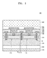
- FIG. 1 is a cross-sectional view illustrating a nitride-based transistor 100 according to a first embodiment of the present disclosure.
- the nitride-based transistor 100 may include a first nitride-based semiconductor layer 105, second nitride-based semiconductor patterns 120 and a third nitride-based semiconductor layer 130.
- the nitride-based transistor 100 may further include trenches 10 disposed in the first nitride-based semiconductor layer 105 between the second nitride-based semiconductor patterns 120.
- the nitride-based transistor 100 may further include a gate dielectric layer 142 and a gate electrode 144 disposed in each of the trenches 10.
- the nitride-based transistor 100 may further include source electrodes 150 electrically connected to the third nitride-based semiconductor layer 130 and a drain electrode 170 electrically connected to the first nitride-based semiconductor layer 105.
- the first nitride-based semiconductor layer 105 may include a nitride layer doped with impurities having a first type.
- the first type may denote a conductivity type of dopants injected into the nitride layer, for example, a semiconductor layer. That is, the first type may be an N-type or a P-type.
- the N-type dopants may be silicon ions and the P-type dopants may be beryllium (Be) ions, magnesium (Mg) ions, calcium (Ca) ions, carbon (C) ions, iron (Fe) ions or manganese (Mn) ions.
- the first nitride-based semiconductor layer 105 may include a nitride layer such as an Al x In y Ga 1-x-y N (where, 0 ⁇ x ⁇ 1 and 0 ⁇ y ⁇ 1) layer.
- the first nitride-based semiconductor layer 105 may be, for example, an N-type GaN layer which is formed using an epitaxial growth technique.
- the second nitride-based semiconductor patterns 120 may be disposed in the first nitride-based semiconductor layer 105. That is, the second nitride-based semiconductor patterns 120 may be surrounded by the first nitride-based semiconductor layer 105. Each of the second nitride-based semiconductor patterns 120 may have a predetermined width, a predetermined length and a predetermined thickness, and the second nitride-based semiconductor patterns 120 may be separated from each other.
- the second nitride-based semiconductor patterns 120 may include a nitride layer doped with dopants having a second type which is different from the first type.
- the second nitride-based semiconductor patterns 120 may be doped to have a P-type.
- the first nitride-based semiconductor layer 105 is doped to have a P-type
- the second nitride-based semiconductor patterns 120 may be doped to have an N-type.
- the third nitride-based semiconductor layer 130 may be disposed on the first nitride-based semiconductor layer 105.
- the third nitride-based semiconductor layer 130 may include a nitride layer heavily doped with dopants having the first type.
- the third nitride-based semiconductor layer 130 may be doped to have the same type as the first nitride-based semiconductor layer 105.
- the third nitride-based semiconductor layer 130 may be electrically connected to the source electrodes 150.
- each of the second nitride-based semiconductor patterns 120 includes a GaN layer doped with dopants having a P-type
- the third nitride-based semiconductor layer 130 includes a GaN layer heavily doped with dopants having an N-type.
- inventive concept is not limited to the following embodiment. That is, the following embodiment may be modified in various different forms to which substantially the same operation as the following embodiment is applied.
- the trenches 10 may be formed in the first nitride-based semiconductor layer 105 between the second nitride-based semiconductor patterns 120.
- the gate dielectric layer 142 and the gate electrode 144 may be disposed in each of the trenches 10.
- the gate dielectric layer 142 may be disposed on sidewalls and bottom surfaces of the trenches 10 in the form of a thin film.
- the gate dielectric layer 142 may include, for example, an oxide layer, a nitride layer or an oxynitride layer. In some embodiments, the gate dielectric layer 142 may include a silicon oxide layer.
- each of the gate electrodes 144 may be disposed on the gate dielectric layer 142, and each of the gate electrodes 144 may be formed to fill one of the trenches 10.
- each of the gate electrodes 144 may include a P-type GaN semiconductor layer doped with beryllium (Be) ions, magnesium (Mg) ions, calcium (Ca) ions, carbon (C) ions, iron (Fe) ions, manganese (Mn) ions, or a combination thereof.
- each of the gate electrodes 144 may include a metal layer such as a nickel (Ni) layer, a gold (Au) layer, a titanium (Ti) layer, an aluminum (Al) layer or the like.
- the gate electrodes 144 may be used in control of a width of depletion regions formed in the first nitride-based semiconductor layer 105 located between the trenches 10 and the second nitride-based semiconductor patterns 120.
- depletion regions 115 may be formed at interface regions between the first nitride-based semiconductor layer 105 and the second nitride-based semiconductor patterns 120 due to P-N junctions.
- the depletion regions 115 are illustrated only in the first nitride-based semiconductor layer 105.
- FIG. 1 if the second nitride-based semiconductor patterns 120 are disposed to directly contact the first nitride-based semiconductor layer 105, depletion regions 115 may be formed at interface regions between the first nitride-based semiconductor layer 105 and the second nitride-based semiconductor patterns 120 due to P-N junctions.
- the depletion regions 115 are illustrated only in the first nitride-based semiconductor layer 105.
- FIG. 1 although not shown in
- additional depletion regions may be formed in the first nitride-based semiconductor layer 105 adjacent to the gate dielectric layer 142 at an equilibrium state due to a work function difference between the gate electrodes 144 and the first nitride-based semiconductor layer 105.
- each of the second nitride-based semiconductor patterns 120 includes a P-type GaN layer
- depletion regions 115 in which electrons are depleted may be formed in the first nitride-based semiconductor layer 105 located between the trenches 10 and the second nitride-based semiconductor patterns 120.
- a width W of the depletion regions 115 may be controlled by applying a gate voltage to the gate electrodes 144.
- a gate voltage e.g., a positive voltage
- the width W of the depletion regions 115 may be reduced to form channel regions (i.e., channel layers) that are located between the trenches 10 and the second nitride-based semiconductor patterns 120 to act as current paths. If the channel layers are formed in a vertical direction, electrons may be drifted from the third nitride-based semiconductor layer 130 toward the drain electrode 170 through the channel layers.
- the source electrodes 150 may be disposed to be physically spaced apart from the gate electrodes 144 and to be in contact with the third nitride-based semiconductor layer 130.
- Each of the source electrodes 150 may include a material exhibiting an ohmic contact with respect to the third nitride-based semiconductor layer 130.
- each of the source electrodes 150 may include a titanium (Ti) layer, an aluminum (Al) layer, a palladium (Pd) layer, a tungsten (W) layer, a nickel (Ni) layer, a chrome (Cr) layer, a platinum (Pt) layer, a gold (Au) layer, a silver (Ag) layer, or an alloy containing at least two thereof. As illustrated in FIG.
- the source electrodes 150 may also be disposed to contact the second nitride-based semiconductor patterns 120.
- the second nitride-based semiconductor patterns 120 and the third nitride-based semiconductor layer 130 may be grounded through the source electrodes 150 when the nitride-based transistor 100 operates. That is, the second nitride-based semiconductor patterns 120 and the third nitride-based semiconductor layer 130 may have a stable potential if a ground voltage is applied to the source electrodes 150.
- An insulation layer 146 may be disposed between the source electrodes 150 and the gate electrodes 142 to electrically insulate the source electrodes 150 from the gate electrodes 142.
- a fourth nitride-based semiconductor layer 160 heavily doped with dopants having the first type may be disposed on a bottom surface of the first nitride-based semiconductor layer 105 opposite to the third nitride-based semiconductor layer 130.
- the fourth nitride-based semiconductor layer 160 may include a GaN layer heavily doped with dopants having the first type.
- the drain electrode 170 may be disposed on a bottom surface of the fourth nitride-based semiconductor layer 160 opposite to the first nitride-based semiconductor layer 105.
- the drain electrode 170 may include a material exhibiting an ohmic contact with respect to the fourth nitride-based semiconductor layer 160.
- the drain electrode 170 may include a titanium (Ti) layer, an aluminum (Al) layer, a palladium (Pd) layer, a tungsten (W) layer, a nickel (Ni) layer, a chrome (Cr) layer, a platinum (Pt) layer, a gold (Au) layer, a silver (Ag) layer, or an alloy containing at least two thereof.
- a heat sink 180 may be disposed on the source electrodes 150.
- the heat sink 180 may be attached to the source electrodes 150 using an adhesion member 182.
- the adhesion member 182 may include a solder material or a metal paste material having an excellent heat conductivity, but not limited thereto.
- the adhesion member 182 may include another adhesion member well known in the art.
- the heat sink 180 may act as a heat radiator for emitting heat generated in the nitride-based transistor 100.
- the heat sink 180 may include a material having an excellent heat conductivity, for example, a metal material.
- the first nitride-based semiconductor layer 105 located between the second nitride-based semiconductor patterns 120 and the gate electrodes 144 may be fully depleted to form the depletion regions 115 at an equilibrium state. Even though an operating voltage is applied between the source electrode 150 and the drain electrode 170 without a gate bias, no carriers may be drifted from the source electrodes 150 toward the drain electrode 170 because of the presence of the depletion regions 115.
- a gate voltage e.g., a positive gate voltage
- a threshold voltage e.g., a positive gate voltage
- the width W of the depletion regions 115 may be reduced or the depletion regions 115 may be removed.
- channel layers may be formed in the first nitride-based semiconductor layer 105 adjacent to sidewalls of the trenches 10.
- the channel layers may be vertically formed in the first nitride-based semiconductor layer 105 adjacent to the sidewalls of the trenches 10 because of the positive gate voltage applied to the gate electrodes 144.
- electrons emitted from the source electrodes 150 may be drifted toward the drain electrode 170 through the third nitride-based semiconductor layer 130, the channel layers, the first nitride-based semiconductor layer 105, and the fourth nitride-based semiconductor layer 160.
- the channel layers controlled by the gate electrodes 144 may be formed in a vertical direction and may be formed in an N-type GaN layer to increase a mobility of carriers (i.e., electrons) drifted therein.
- a nitride-based transistor including a first N-type nitride-based region (acting as a source region), a P-type nitride-based region (acting as a channel body), and a second N-type nitride-based region (acting as a drain region) may be proposed.
- an N-type channel layer may be formed in the P-type nitride-based region using a gate bias.
- the P-type nitride-based region may be formed by doping a GaN layer with P-type dopants such as magnesium (Mg) ions.
- P-type dopants such as magnesium (Mg) ions.
- Mg magnesium
- a dose of the P-type dopants has to increase to obtain a high threshold voltage appropriate for a high voltage operation.
- a nitride-based transistor including a first N-type nitride-based region (acting as a source region), a P-type nitride-based region (acting as a channel body), and a second N-type nitride-based region (acting as a drain region) may be proposed and a two-dimension electron gas (2DEG) layer may be formed between the P-type nitride-based region and a gate electrode due to a junction of an AlGaN layer and a GaN layer.
- 2DEG acts as a channel layer, a channel mobility may be improved.
- a threshold voltage of the nitride-based transistor according to the second comparative example may be too low to use the nitride-based transistor as a high voltage transistor. That is, it may be difficult to modulate the 2DEG layer acting as a channel layer with a gate bias. For example, it may be difficult to obtain a threshold voltage higher than 3 volts.
- the depletion regions 115 may be formed in the first nitride-based semiconductor layer 105 adjacent to the gate electrode 144 at an equilibrium state and a width of the depletion regions 115 may be modulated by a gate voltage applied to the gate electrodes 144.
- a channel mobility may be improved and a high threshold voltage over 3 volts may be obtained.
- the embodiment described with reference to FIG. 1 may overcome the disadvantages (e.g., a low channel mobility and a low threshold voltage) of the first and second comparative examples.
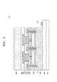
- FIG. 2 is a cross-sectional view illustrating a nitride-based transistor 200 according to a second embodiment of the present disclosure.
- the nitride-based transistor 200 may have substantially the same configuration as the nitride-based transistor 100 illustrated in FIG. 1 except that the fourth nitride-based semiconductor layer 160 is disposed on a substrate 101 and a drain electrode 270 is disposed on a portion of the fourth nitride-based semiconductor layer 160.
- the substrate 101 may be one selected from the group consisting of a sapphire substrate, a GaN substrate, a silicon carbide (SiC) substrate, a silicon substrate and an aluminum nitride (AlN) substrate.
- these substrates are merely examples of suitable substrates for the nitride-based transistor 200. Any substrate having an electrical insulation property can also be used as the substrate 101.
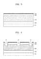
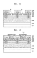
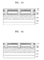
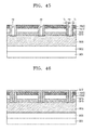
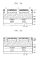
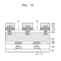
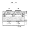
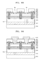
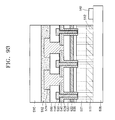
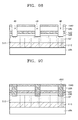
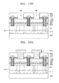
- FIGS. 3 to 14 are cross-sectional views illustrating a method of fabricating a nitride-based transistor according to an embodiment of the present disclosure.
- a nitride-based semiconductor layer may include a nitride material such as an Al x In y Ga 1-x-y N (where, 0 ⁇ x ⁇ 1 and 0 ⁇ y ⁇ 1) layer.
- the nitride-based semiconductor layer may be formed using a metal organic chemical vapor deposition (MOCVD) process, a molecular beam epitaxy (MBE) process, or a hydride vapor phase epitaxy process.
- MOCVD metal organic chemical vapor deposition
- MBE molecular beam epitaxy
- a first nitride-based semiconductor layer 305 doped with dopants having a first type, a second nitride-based semiconductor layer 320 doped with dopants having a second type, and a third nitride-based semiconductor layer 330 doped with dopants having the first type may be sequentially formed on a substrate 301.
- a lower nitride-based semiconductor layer heavily doped with dopants having the first type may be additionally formed between the substrate 301 and the first nitride-based semiconductor layer 305.
- the substrate 301 may be one selected from the group consisting of a sapphire substrate, a GaN substrate, a SiC substrate, a silicon substrate, and an AlN substrate.
- the substrate 301 is not limited to the above-listed substrates.
- any substrate on which a nitride-based layer can be grown may also be used as the substrate 301.
- the first nitride-based semiconductor layer 305, the second nitride-based semiconductor layer 320, and the third nitride-based semiconductor layer 330 may be formed of the same material layer except for the conductivity type. If the first type is an N-type, the second type may be a P-type. On the contrary, if the first type is a P-type, the second type may be an N-type.
- the dopants having an N-type may include silicon ions and the dopants having a P-type may include beryllium (Be) ions, magnesium (Mg) ions, calcium (Ca) ions, carbon (C) ions, iron (Fe) ions and manganese (Mn) ions.
- first trenches 20 may be formed to penetrate the third and second nitride-based semiconductor layers 330 and 320 and to extend into the first nitride-based semiconductor layer 305.
- the first trenches 20 may be formed by etching the third, second and first nitride-based semiconductor layers 330, 320 and 305.
- Each of the first trenches 20 may be formed to include a bottom surface and sidewalls perpendicular to the bottom surface.
- each of the first trenches 20 may be formed to include a bottom surface and sidewalls non-perpendicular to the bottom surface. In such a case, the sidewalls of the first trenches 20 may have a sloped profile.
- a tilt angle of the sloped sidewalls of the first trenches 20 to the bottom surfaces of the first trenches 20 may be different according to the etch process for forming the first trenches 20.
- the tilt angle of the sloped sidewalls of the first trenches 20 to the bottom surfaces of the first trenches 20 may be within a range of about 30 degrees to about 90 degrees according to a lattice plane of the first, second and third nitride-based semiconductor layers 305, 320 and 330 (e.g., GaN layers).
- the tilt angle of the sloped sidewalls of the first trenches 20 to the bottom surfaces of the first trenches 20 may be within a range of about 60 degrees to about 70 degrees when the first trenches 20 are formed using a dry etch process or a wet etch process.
- a fourth nitride-based semiconductor layer 340 doped with dopants having the first type may be formed on the third nitride-based semiconductor layer 330 to fill the first trenches 20. That is, the fourth nitride-based semiconductor layer 340 may be formed in the first trenches 20 and on the third nitride-based semiconductor layer 330. Subsequently, an upper nitride-based semiconductor layer 360 heavily doped with dopants having the first type may be formed on the fourth nitride-based semiconductor layer 340.
- the fourth nitride-based semiconductor layer 340 may be formed of an N-type GaN layer having an impurity concentration of about 1 ⁇ 10 16 /cm 3 to about 1 ⁇ 10 17 /cm 3
- the upper nitride-based semiconductor layer 360 may be formed of an N-type GaN layer having an impurity concentration which is equal to or higher than 1 ⁇ 10 18 /cm 3
- the second nitride-based semiconductor patterns 320 may be surrounded by the first nitride-based semiconductor layer 305, the third nitride-based semiconductor patterns 330 and the fourth nitride-based semiconductor layer 340.
- the upper nitride-based semiconductor layer 360 and the fourth nitride-based semiconductor layer 340 may be patterned to form second trenches 30.
- the second trenches 30 may be formed in respective ones of the first trenches 20.
- the second trenches 30 may be formed by etching the upper nitride-based semiconductor layer 360 and the fourth nitride-based semiconductor layer 340 such that portions of the fourth nitride-based semiconductor layer 340 remain on the sidewalls of the first trenches 20 to have a predetermined thickness.
- the remaining portions of the fourth nitride-based semiconductor layer 340 on the sidewalls of the first trenches 20 may act as channel body layers of the nitride-based transistor.
- a thickness (i.e., a width in a horizontal direction) of the remaining portions of the fourth nitride-based semiconductor layer 340 on the sidewalls of the first trenches 20 may be determined in consideration of a width of depletion regions which are formed between the second nitride-based semiconductor patterns 320 and gate electrodes to be formed in the second trenches 30.
- the second trenches 30 may be formed to have bottom surfaces whose levels are lower than levels of bottom surfaces of the second nitride-based semiconductor patterns 320.
- FIG. 6 illustrates an example in which bottom surfaces of the second trenches 30 are coplanar with bottom surfaces of the first trenches 20, the inventive concept is not limited thereto.
- the second trenches 30 may be formed such that a level of the bottom surfaces of the second trenches 30 is lower or higher than a level of the bottom surfaces of the first trenches 20.
- the second trenches 30 may be formed such that the sidewalls of the second trenches 30 are perpendicular to the bottom surfaces of the second trenches 30.
- the second trenches 30 may be formed such that the sidewalls of the second trenches 30 are non-perpendicular to the bottom surfaces of the second trenches 30.
- the sidewalls of the second trenches 30 may have a sloped profile. A tilt angle of the sloped sidewalls of the second trenches 30 to the bottom surfaces of the second trenches 30 may be different according to the etch process for forming the second trenches 30.
- the tilt angle of the sloped sidewalls of the second trenches 30 to the bottom surfaces of the second trenches 30 may be within a range of about 30 degrees to about 90 degrees according to a lattice plane of the fourth and upper nitride-based semiconductor layers 340 and 360 (e.g., GaN layers). In some embodiments, the tilt angle of the sloped sidewalls of the second trenches 30 to the bottom surfaces of the second trenches 30 may be within a range of about 60 degrees to about 70 degrees when the second trenches 30 are formed using a dry etch process or a wet etch process.
- the upper nitride-based semiconductor layer 360, the fourth nitride-based semiconductor layer 340 and the third nitride-based semiconductor patterns 330 may be etched to form third trenches 40 that are disposed between the second trenches 30 to expose portions of the second nitride-based semiconductor patterns 320.
- the third trenches 40 may be formed such that sidewalls of the third trenches 40 are perpendicular to bottom surfaces of the third trenches 40.
- the third trenches 40 may be formed such that the sidewalls of the third trenches 40 are non-perpendicular to the bottom surfaces of the third trenches 40. That is, the sidewalls of the third trenches 40 may have a sloped profile.
- the third trenches 40 may function as source contact holes in which source electrodes 380 are formed in a subsequent process.
- a gate dielectric layer 372 may be formed in the second and third trenches 30 and 40 and on the upper nitride-based semiconductor layer 360. As illustrated in FIG. 8 , the gate dielectric layer 372 may be formed to fill the third trenches 40, but the gate dielectric layer 372 may be conformably formed in the second trenches 30.
- the gate dielectric layer 372 may be formed to include an oxide layer, a nitride layer or an oxynitride layer.
- the gate dielectric layer 372 may be formed using a CVD process, a sputtering process, an atomic layer deposition (ALD) process or an evaporation process.
- a gate conductive layer may be formed on the gate dielectric layer 372 to fill the second trenches 30.
- the gate conductive layer may be patterned to form gate electrodes 374 covering the second trenches 30.
- the gate conductive layer may be formed to include a GaN layer doped with P-type dopants such as beryllium (Be) ions, magnesium (Mg) ions, calcium (Ca) ions, carbon (C) ions, iron (Fe) ions, manganese (Mn) ions, or mixed ions containing at least two different ions among the above-listed ions.
- Be beryllium
- Mg magnesium
- Ca calcium
- C carbon
- Fe iron
- Mn manganese
- gate conductive layer may be formed to include a metal layer such as a nickel (Ni) layer, a gold (Au) layer, a titanium (Ti) layer or an aluminum (Al) layer.
- the gate conductive layer may be formed using a CVD process, a sputtering process, an ALD process or an evaporation process.
- an interlayer insulation layer 376 may be formed on the gate dielectric layer 372 and the gate electrodes 374.
- the interlayer insulation layer 376 may be formed to include an oxide layer, a nitride layer or an oxynitride layer.
- the interlayer insulation layer 376 may be formed using a CVD process, a sputtering process, an ALD process or an evaporation process.
- the interlayer insulation layer 376 and the gate dielectric layer 372 may be etched to form interlayer insulation patterns 378 and gate dielectric patterns 373.
- the gate dielectric layer 372 in the third trenches 40 may be removed to expose the sidewalls and bottom surfaces of the third trenches 40. That is, the interlayer insulation layer 376 and the gate dielectric layer 372 may be etched to expose portions of the second nitride-based semiconductor patterns 320.
- the third trenches 40 may function as source contact holes in which source electrodes 380 are formed in a subsequent process.
- source electrodes 380 may be formed in the source contact holes 40.
- the source electrodes 380 may be formed to extend into gap regions between the interlayer insulation patterns 378.
- the source electrodes 380 may be formed of a material exhibiting an ohmic contact with respect to the third nitride-based semiconductor patterns 330, the fourth nitride-based semiconductor layer 340 or the upper nitride-based semiconductor patterns 360.
- the source electrodes 380 may be formed to include a titanium (Ti) layer, an aluminum (Al) layer, a palladium (Pd) layer, a tungsten (W) layer, a nickel (Ni) layer, a chrome (Cr) layer, a platinum (Pt) layer, a gold (Au) layer, a silver (Ag) layer, or an alloy containing at least two thereof.
- the source electrodes 380 may be formed using a CVD process, a sputtering process, an ALD process or an evaporation process.
- a heat sink 910 may be formed on the source electrodes 380.
- the heat sink 910 may act as a heat radiator for emitting heat generated in a nitride-based transistor.
- the heat sink 910 may be formed to include a material having an excellent heat conductivity, for example, a metal material.
- the heat sink 910 may be attached to the source electrodes 380 using an adhesion member 912.
- the adhesion member 912 may include a solder material or a metal paste material having an excellent heat conductivity, but not limited thereto.
- the adhesion member 912 may include another adhesion member well known in the art.
- the substrate 301 may be detached from the lower nitride-based semiconductor layer 302.
- the substrate 301 may be detached from the lower nitride-based semiconductor layer 302 using a laser lift-off process.
- a drain electrode 390 may be formed on the exposed surface of the lower nitride-based semiconductor layer 302 opposite to the first nitride-based semiconductor layer 305.
- the drain electrode 390 may be formed of a material exhibiting an ohmic contact with respect to the lower nitride-based semiconductor layer 302.
- the drain electrode 390 may be formed to include a titanium (Ti) layer, an aluminum (Al) layer, a palladium (Pd) layer, a tungsten (W) layer, a nickel (Ni) layer, a chrome (Cr) layer, a platinum (Pt) layer, a gold (Au) layer, a silver (Ag) layer, or an alloy containing at least two thereof.
- the drain electrode 390 may be formed using a CVD process, a sputtering process, an ALD process or an evaporation process.
- a nitride-based transistor according to an embodiment may be fabricated through the aforementioned processes.
- the first, second, third, fourth and upper nitride-based semiconductor layers 305, 320, 330, 340 and 360 may be patterned to expose a portion of the lower nitride-based semiconductor layer 302.
- the drain electrode 390 may be formed on the exposed portion of the lower nitride-based semiconductor layer 302.
- a heat sink may also be additionally formed on the source electrodes 380.
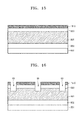
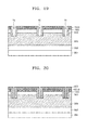
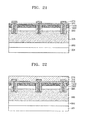
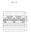
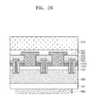
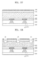
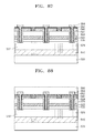
- FIGS. 15 to 26 are cross-sectional views illustrating a method of fabricating a nitride-based transistor according to another embodiment of the present disclosure.
- a nitride-based semiconductor layer may include a nitride material such as an Al x In y Ga 1-x-y N (where, 0 ⁇ x ⁇ 1 and 0 ⁇ y ⁇ 1) layer.
- the nitride-based semiconductor layer may be formed using a metal organic chemical vapor deposition (MOCVD) process, a molecular beam epitaxy (MBE) process, or a hydride vapor phase epitaxy process.
- MOCVD metal organic chemical vapor deposition
- MBE molecular beam epitaxy
- hydride vapor phase epitaxy process a hydride vapor phase epitaxy
- a lower nitride-based semiconductor layer 302 heavily doped with dopants having a first type, a first nitride-based semiconductor layer 305 doped with dopants having the first type, a second nitride-based semiconductor layer 320 doped with dopants having a second type, and an upper nitride-based semiconductor layer 1510 heavily doped with dopants having the first type may be sequentially formed on a substrate 301.
- the lower nitride-based semiconductor layer 302 may be formed of a GaN layer heavily doped with N-type dopants
- the first nitride-based semiconductor layer 305 may be formed of a GaN layer lightly doped with N-type dopants
- the second nitride-based semiconductor layer 320 may be formed of a GaN layer doped with P-type dopants
- the upper nitride-based semiconductor layer 1510 may be formed of a GaN layer heavily doped with N-type dopants.
- the lower nitride-based semiconductor layer 302 and the upper nitride-based semiconductor layer 1510 may be doped to have an impurity concentration which is equal to or higher than about 1 ⁇ 10 18 /cm 3
- the first nitride-based semiconductor layer 305 may be doped to have an impurity concentration of about 1 ⁇ 10 16 /cm 3 to about 1 ⁇ 10 17 /cm 3 .
- first trenches 60 may be formed to penetrate the upper and second nitride-based semiconductor layers 1510 and 320 and to extend into the first nitride-based semiconductor layer 305.
- the first trenches 60 may be formed by etching the upper, second and first nitride-based semiconductor layers 1510, 320 and 305.
- Each of the first trenches 60 may be formed to include a bottom surface and sidewalls perpendicular to the bottom surface.
- each of the first trenches 60 may be formed to include a bottom surface and sidewalls non-perpendicular to the bottom surface. In such a case, the sidewalls of the first trenches 60 may have a sloped profile.
- a third nitride-based semiconductor layer 1520 doped with dopants having the first type may be formed on the upper nitride-based semiconductor layer 1510 to fill the first trenches 60. That is, the third nitride-based semiconductor layer 1520 may be formed in the first trenches 60 and on the upper nitride-based semiconductor layer 1510. In some embodiments, the third nitride-based semiconductor layer 1520 may be formed of an N-type GaN layer having an impurity concentration of about 1 ⁇ 10 16 /cm 3 to about 1 ⁇ 10 17 /cm 3 .
- the second nitride-based semiconductor patterns 320 may be surrounded by the first nitride-based semiconductor layer 305, the upper nitride-based semiconductor patterns 1510 and the third nitride-based semiconductor layer 1520.
- the third nitride-based semiconductor layer 1520 may be planarized to expose top surfaces of the upper nitride-based semiconductor patterns 1510.
- the third nitride-based semiconductor layer 1520 may be planarized using a chemical mechanical polishing (CMP) process, a dry etch process or a wet etch process.
- CMP chemical mechanical polishing
- the third nitride-based semiconductor patterns 1520 in the first trenches 60 may be patterned to form second trenches 70.
- the second trenches 70 may be formed in respective ones of the first trenches 60. More specifically, the second trenches 70 may be formed by etching the third nitride-based semiconductor patterns 1520 such that portions of the third nitride-based semiconductor patterns 1520 remain on the sidewalls of the first trenches 60 to have a predetermined thickness. The remaining portions of the third nitride-based semiconductor patterns 1520 on the sidewalls of the first trenches 60 may act as channel body layers of the nitride-based transistor.
- a thickness (i.e., a width in a horizontal direction) of the remaining portions of the third nitride-based semiconductor layer 1520 on the sidewalls of the first trenches 60 may be determined in consideration of a width of depletion regions which are formed between the second nitride-based semiconductor patterns 320 and gate electrodes to be formed in the second trenches 70.
- FIG. 19 illustrates an example in which bottom surfaces of the second trenches 70 are coplanar with bottom surfaces of the first trenches 60
- the inventive concept is not limited thereto.
- the second trenches 70 may be formed such that a level of the bottom surfaces of the second trenches 70 is lower or higher than a level of the bottom surfaces of the first trenches 60.
- a gate dielectric layer 372 may be formed in the second trenches 70 and on the upper nitride-based semiconductor patterns 1510. As illustrated in FIG. 20 , the gate dielectric layer 372 may be conformably formed in the second trenches 70.
- a gate conductive layer may be formed on the gate dielectric layer 372 to fill the second trenches 70.
- the gate conductive layer may be patterned to form gate electrodes 374 covering the second trenches 70.
- an interlayer insulation layer 376 may be formed on the gate dielectric layer 372 and the gate electrodes 374.
- the interlayer insulation layer 376, the gate dielectric layer 372 and the upper nitride-based semiconductor patterns 1510 may be patterned to form insulation patterns 378 and gate dielectric patterns 373.
- third trenches 80 may be formed to expose portions of the second nitride-based semiconductor patterns 320.
- the third trenches 80 may function as source contact holes in which source electrodes 380 are formed in a subsequent process.
- source electrodes 380 may be formed in the source contact holes 80.
- the source electrodes 380 may be formed to extend into gap regions between the insulation patterns 378.
- the source electrodes 380 may be formed of a material exhibiting an ohmic contact with respect to the upper nitride-based semiconductor patterns 1510.
- a heat sink 910 may be formed on the source electrodes 380.
- the heat sink 910 may act as a heat radiator for emitting heat generated in the nitride-based transistor.
- the heat sink 910 may be attached to the source electrodes 380 using an adhesion member 912.
- the adhesion member 912 may include a solder material or a metal paste material having an excellent heat conductivity, but not limited thereto.
- the adhesion member 912 may include another adhesion member well known in the art.
- the substrate 301 may be detached from the lower nitride-based semiconductor layer 302.
- the substrate 301 may be detached from the lower nitride-based semiconductor layer 302 using a laser lift-off process.
- a drain electrode 390 may be formed on the exposed surface of the lower nitride-based semiconductor layer 302 opposite to the first nitride-based semiconductor layer 305.
- the drain electrode 390 may be formed of a material exhibiting an ohmic contact with respect to the lower nitride-based semiconductor layer 302.
- a nitride-based transistor according to an embodiment may be fabricated through the aforementioned processes.
- the first, second and upper nitride-based semiconductor layers 305, 320 and 1510 may be patterned to expose a portion of the lower nitride-based semiconductor layer 302.
- the drain electrode 390 may be formed on the exposed portion of the lower nitride-based semiconductor layer 302.
- a nitride-based transistor having substantially the same configuration as the nitride-based transistor 200 illustrated in FIG. 2 can be fabricated.
- a heat sink may also be additionally formed on the source electrodes 380.
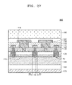
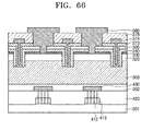
- FIG. 27 is a cross-sectional view illustrating a vertical nitride-based transistor 300 according to a third embodiment of the present disclosure.
- the vertical nitride-based transistor 300 may include a first nitride-based semiconductor layer 105, a current blocking insulation patterns 110, second nitride-based semiconductor patterns 120 and a third nitride-based semiconductor layer 130.
- the vertical nitride-based transistor 300 may further include trenches 10 disposed in the first nitride-based semiconductor layer 105 between the second nitride-based semiconductor patterns 120.
- the vertical nitride-based transistor 300 may further include a gate dielectric layer 142 and a gate electrode 144 disposed in each of the trenches 10. Furthermore, the vertical nitride-based transistor 300 may further include source electrodes 150 electrically connected to the third nitride-based semiconductor layer 130 and a drain electrode 170 electrically connected to the first nitride-based semiconductor layer 105.
- the first nitride-based semiconductor layer 105 may include a nitride layer doped with impurities having a first type.
- the first type may denote a conductivity type of dopants injected into the nitride layer, for example, a semiconductor layer. That is, the first type may be an N-type or a P-type.
- the N-type dopants may be silicon ions and the P-type dopants may be beryllium (Be) ions, magnesium (Mg) ions, calcium (Ca) ions, carbon (C) ions, iron (Fe) ions or manganese (Mn) ions.
- the first nitride-based semiconductor layer 105 may include a nitride layer such as an Al x In y Ga 1-x-y N (where, 0 ⁇ x ⁇ 1 and 0 ⁇ y ⁇ 1) layer.
- the first nitride-based semiconductor layer 105 may be, for example, an N-type GaN layer which is formed using an epitaxial growth technique.
- the second nitride-based semiconductor patterns 120 may be disposed in the first nitride-based semiconductor layer 105. That is, the second nitride-based semiconductor patterns 120 may be surrounded by the first nitride-based semiconductor layer 105. Each of the second nitride-based semiconductor patterns 120 may have a predetermined width, a predetermined length and a predetermined thickness, and the second nitride-based semiconductor patterns 120 may be separated from each other.
- the second nitride-based semiconductor patterns 120 may include a nitride layer doped with dopants having a second type which is different from the first type.
- the second nitride-based semiconductor patterns 120 may be doped to have a P-type.
- the first nitride-based semiconductor layer 105 is doped to have a P-type
- the second nitride-based semiconductor patterns 120 may be doped to have an N-type.
- Current blocking insulation patterns 110 may be disposed between the first nitride-based semiconductor layer 105 and bottom surfaces of the second nitride-based semiconductor patterns 120.
- Each of the current blocking insulation patterns 110 may include a nitride-based semiconductor material doped with carbon ions or iron ions.
- each of the current blocking insulation patterns 110 may include a GaN material doped with carbon ions or iron ions.
- the current blocking insulation patterns 110 may prevent leakage currents between the source electrodes 150 and the drain electrode 170 from flowing through the second nitride-based semiconductor patterns 120.
- All of the first nitride-based semiconductor layer 105, second nitride-based semiconductor patterns 120, and the current blocking insulation patterns 110 may be formed of the same nitride-based semiconductor material, for example, a GaN material. That is, the first nitride-based semiconductor layer 105, second nitride-based semiconductor patterns 120 and the current blocking insulation patterns 110 may have the same lattice constant. Thus, no deformation occurs in the first nitride-based semiconductor layer 105, second nitride-based semiconductor patterns 120 and the current blocking insulation patterns 110 because the first nitride-based semiconductor layer 105, second nitride-based semiconductor patterns 120 and the current blocking insulation patterns 110 have the same lattice constant.
- the third nitride-based semiconductor layer 130 may be disposed on the first nitride-based semiconductor layer 105.
- the third nitride-based semiconductor layer 130 may include a nitride layer heavily doped with dopants having the first type.
- the third nitride-based semiconductor layer 130 may be doped to have the same type as the first nitride-based semiconductor layer 105.
- the third nitride-based semiconductor layer 130 may be electrically connected to the source electrodes 150.
- each of the current blocking insulation patterns 110 includes a GaN layer doped with carbon ions or iron ions
- each of the second nitride-based semiconductor patterns 120 includes a GaN layer doped with dopants having a P-type
- the third nitride-based semiconductor layer 130 includes a GaN layer heavily doped with dopants having an N-type.
- inventive concept is not limited to the following embodiment. That is, the following embodiment may be modified in various different forms to which substantially the same operation as the following embodiment is applied.
- the trenches 10 may be formed in the first nitride-based semiconductor layer 105 between the second nitride-based semiconductor patterns 120.
- the gate dielectric layer 142 and the gate electrode 144 may be disposed in each of the trenches 10.
- the gate dielectric layer 142 may be disposed on sidewalls and bottom surfaces of the trenches 10 in the form of a thin film.
- the gate dielectric layer 142 may include, for example, an oxide layer, a nitride layer or an oxynitride layer. In some embodiments, the gate dielectric layer 142 may include a silicon oxide layer.
- each of the gate electrodes 144 may be disposed on the gate dielectric layer 142, and each of the gate electrodes 144 may be formed to fill one of the trenches 10.
- each of the gate electrodes 144 may include a P-type GaN semiconductor layer doped with beryllium (Be) ions, magnesium (Mg) ions, calcium (Ca) ions, carbon (C) ions, iron (Fe) ions, manganese (Mn) ions, or a combination thereof.
- each of the gate electrodes 144 may include a metal layer such as a nickel (Ni) layer, a gold (Au) layer, a titanium (Ti) layer, an aluminum (Al) layer or the like.
- the gate electrodes 144 may be used in control of a width of depletion regions formed in the first nitride-based semiconductor layer 105 located between the trenches 10 and the second nitride-based semiconductor patterns 120. As illustrated in FIG. 27 , if the second nitride-based semiconductor patterns 120 are disposed to directly contact the first nitride-based semiconductor layer 105, depletion regions 115 may be formed at interface regions between the first nitride-based semiconductor layer 105 and the second nitride-based semiconductor patterns 120 due to P-N junctions.
- additional depletion regions may be formed in the first nitride-based semiconductor layer 105 adjacent to the gate dielectric layer 142 at an equilibrium state due to a work function difference between the gate electrodes 144 and the first nitride-based semiconductor layer 105.
- FIG. 27 illustrates depletion regions 115 which are formed in the first nitride-based semiconductor layer 105 because of presence of the second nitride-based semiconductor patterns 120 and the gate electrodes 144.
- first nitride-based semiconductor layer 105 includes an N-type GaN layer and each of the second nitride-based semiconductor patterns 120 includes a P-type GaN layer, electrons may be depleted in the depletion regions 115 which are formed in the first nitride-based semiconductor layer 105 located between the trenches 10 and the second nitride-based semiconductor patterns 120.
- a width W1 and a width W2 of the depletion regions 115 adjacent to the sidewalls of the trenches 10 may be controlled by applying a gate voltage to the gate electrodes 144.
- a gate voltage e.g., a positive voltage
- the widths W1 and W2 of the depletion regions 115 may be reduced to form channel regions (i.e., channel layers) that are located between the trenches 10 and the second nitride-based semiconductor patterns 120 to act as current paths. If the channel layers are formed in a vertical direction, electrons may be drifted from the third nitride-based semiconductor layer 130 toward the drain electrode 170 through the channel layers.
- the source electrodes 150 may be disposed to be physically spaced apart from the gate electrodes 144 and to be in contact with the third nitride-based semiconductor layer 130.
- Each of the source electrodes 150 may include a material exhibiting an ohmic contact with respect to the third nitride-based semiconductor layer 130.
- each of the source electrodes 150 may include a titanium (Ti) layer, an aluminum (Al) layer, a palladium (Pd) layer, a tungsten (W) layer, a nickel (Ni) layer, a chrome (Cr) layer, a platinum (Pt) layer, a gold (Au) layer, a silver (Ag) layer, or an alloy containing at least two thereof. As illustrated in FIG.
- the source electrodes 150 may also be disposed to contact the second nitride-based semiconductor patterns 120.
- the second nitride-based semiconductor patterns 120 and the third nitride-based semiconductor layer 130 may be grounded through the source electrodes 150 when the nitride-based transistor 100 operates. That is, the second nitride-based semiconductor patterns 120 and the third nitride-based semiconductor layer 130 may have a stable potential if a ground voltage is applied to the source electrodes 150.
- An insulation layer 146 may be disposed between the source electrodes 150 and the gate electrodes 142 to electrically insulate the source electrodes 150 from the gate electrodes 142.
- a fourth nitride-based semiconductor layer 160 heavily doped with dopants having the first type may be disposed on a bottom surface of the first nitride-based semiconductor layer 105 opposite to the third nitride-based semiconductor layer 130.
- the fourth nitride-based semiconductor layer 160 may include a GaN layer heavily doped with dopants having the first type.
- the drain electrode 170 may be disposed on a bottom surface of the fourth nitride-based semiconductor layer 160 opposite to the first nitride-based semiconductor layer 105.
- the drain electrode 170 may include a material exhibiting an ohmic contact with respect to the fourth nitride-based semiconductor layer 160.
- the drain electrode 170 may include a titanium (Ti) layer, an aluminum (Al) layer, a palladium (Pd) layer, a tungsten (W) layer, a nickel (Ni) layer, a chrome (Cr) layer, a platinum (Pt) layer, a gold (Au) layer, a silver (Ag) layer, or an alloy containing at least two thereof.
- a heat sink 180 may be disposed on the source electrodes 150.
- the heat sink 180 may be attached to the source electrodes 150 using an adhesion member 182.
- the adhesion member 182 may include a solder material or a metal paste material having an excellent heat conductivity, but not limited thereto.
- the adhesion member 182 may include another adhesion member well known in the art.
- the heat sink 180 may act as a heat radiator for emitting heat generated in the nitride-based transistor 300.
- the heat sink 180 may include a material having an excellent heat conductivity, for example, a metal material.
- the first nitride-based semiconductor layer 105 located between the second nitride-based semiconductor patterns 120 and the gate electrodes 144 may be fully depleted to form the depletion regions 115 at an equilibrium state.
- an operating voltage is applied between the source electrode 150 and the drain electrode 170 without a gate bias, no carriers may be drifted from the source electrodes 150 toward the drain electrode 170 because of the presence of the depletion regions 115.
- a gate voltage e.g., a positive gate voltage
- a threshold voltage e.g., a positive gate voltage
- the widths W1 and W2 of the depletion regions 115 may be reduced or the depletion regions 115 may be removed.
- channel layers may be formed in the first nitride-based semiconductor layer 105 adjacent to sidewalls of the trenches 10.
- the channel layers may be vertically formed in the first nitride-based semiconductor layer 105 adjacent to the sidewalls of the trenches 10 because of the positive gate voltage applied to the gate electrodes 144.
- electrons emitted from the source electrodes 150 may be drifted toward the drain electrode 170 through the third nitride-based semiconductor layer 130, the channel layers, the first nitride-based semiconductor layer 105, and the fourth nitride-based semiconductor layer 160.
- the channel layers controlled by the gate electrodes 144 may be formed in a vertical direction and may be formed in an N-type GaN layer to increase a mobility of carriers (i.e., electrons) drifted therein.
- a nitride-based transistor including a first N-type nitride-based region (acting as a source region), a P-type nitride-based region (acting as a channel body), and a second N-type nitride-based region (acting as a drain region) may be proposed.
- an N-type channel layer may be formed in the P-type nitride-based region using a gate bias.
- the P-type nitride-based region may be formed by doping a GaN layer with P-type dopants such as magnesium (Mg) ions.
- P-type dopants such as magnesium (Mg) ions.
- Mg magnesium
- a dose of the P-type dopants has to increase to obtain a high threshold voltage appropriate for a high voltage operation.
- a nitride-based transistor including a first N-type nitride-based region (acting as a source region), a P-type nitride-based region (acting as a channel body), and a second N-type nitride-based region (acting as a drain region) may be proposed, and a two-dimension electron gas (2DEG) layer may be formed between the P-type nitride-based region and a gate electrode due to a junction of an AlGaN layer and a GaN layer.
- 2DEG two-dimension electron gas
- a threshold voltage of the nitride-based transistor according to the second comparative example may be too low to use the nitride-based transistor as a high voltage transistor. That is, it may be difficult to modulate the 2DEG layer acting as a channel layer with a gate bias. For example, it may be difficult to obtain a threshold voltage higher than 3 volts.
- the depletion regions 115 may be formed in the first nitride-based semiconductor layer 105 adjacent to the gate electrode 144 at an equilibrium state and a width of the depletion regions 115 may be modulated by a gate voltage applied to the gate electrodes 144.
- a channel mobility may be improved and a high threshold voltage over 3 volts may be obtained.
- the embodiment described with reference to FIG. 27 may overcome the disadvantages (e.g., a low channel mobility and a low threshold voltage) of the first and second comparative examples.
- the current blocking insulation patterns 110 may be disposed under the second nitride-based semiconductor patterns 120 to block the leakage currents that flow from the source electrode 150 toward the drain electrode 170 through the second nitride-based semiconductor patterns 120.
- the current blocking insulation patterns 110 may include a nitride-based material having the substantially the same lattice constant as the first nitride-based semiconductor layer 105 and the second nitride-based semiconductor patterns 120.
- FIG. 28 is a cross-sectional view illustrating a nitride-based transistor 400 according to a fourth embodiment of the present disclosure.
- the nitride-based transistor 400 may have substantially the same configuration as the nitride-based transistor 300 illustrated in FIG. 27 except that the fourth nitride-based semiconductor layer 160 is disposed on a substrate 101 and a drain electrode 270 is disposed on a portion of the fourth nitride-based semiconductor layer 160.
- the substrate 101 may be one selected from the group consisting of a sapphire substrate, a GaN substrate, a silicon carbide (SiC) substrate, a silicon substrate and an aluminum nitride (AlN) substrate.
- these substrates are merely examples of suitable substrates for the nitride-based transistor 400. Any substrate having an electrical insulation property can also be used as the substrate 101.
- FIGS. 29 to 40 are cross-sectional views illustrating a method of fabricating a nitride-based transistor according to yet another embodiment of the present disclosure.
- a nitride-based semiconductor layer may include a nitride material such as an Al x In y Ga 1-x-y N (where, 0 ⁇ x ⁇ 1 and 0 ⁇ y ⁇ 1) layer.
- the nitride-based semiconductor layer may be formed using a MOCVD process, an MBE process, or a hydride vapor phase epitaxy process.
- a first nitride-based semiconductor layer 305 doped with dopants having a first type, a current blocking insulation layer 310, a second nitride-based semiconductor layer 320 doped with dopants having a second type, and a third nitride-based semiconductor layer 330 doped with dopants having the first type may be sequentially formed on a substrate 301.
- a lower nitride-based semiconductor layer 302 heavily doped with dopants having the first type may be additionally formed between the substrate 301 and the first nitride-based semiconductor layer 305. That is, an impurity concentration of the lower nitride-based semiconductor layer 302 may be higher than that of the first nitride-based semiconductor layer 305.
- the substrate 301 may be one selected from the group consisting of a sapphire substrate, a GaN substrate, a silicon carbide (SiC) substrate, a silicon substrate and an aluminum nitride (AlN) substrate.
- these substrates are merely examples of suitable substrates for fabrication of the nitride-based transistor. That is, any substrate on which a nitride-based layer can be grown may also be used as the substrate 301.
- the first nitride-based semiconductor layer 305, the second nitride-based semiconductor layer 320, and the third nitride-based semiconductor layer 330 may be formed of the same material layer except for the conductivity type. If the first type is an N-type, the second type may be a P-type. On the contrary, if the first type is a P-type, the second type may be an N-type.
- the dopants having an N-type may include silicon ions and the dopants having a P-type may include beryllium (Be) ions, magnesium (Mg) ions, calcium (Ca) ions, carbon (C) ions, iron (Fe) ions and manganese (Mn) ions.
- the current blocking insulation layer 310 may include a nitride-based semiconductor material doped with carbon ions or iron ions.
- a carbon tetrabromide (CBr 4 ) gas or a carbon tetrachloride (CCl 4 ) gas may be used as a dopant gas for producing carbon ions.
- a bis(cyclopentadienyl)iron (Cp2Fe) material may be used as a precursor for producing iron ions.
- first trenches 22 may be formed to penetrate the third and second nitride-based semiconductor layers 330 and 320 as well as the current blocking insulation layer 310 and to extend into the first nitride-based semiconductor layer 305.
- the first trenches 22 may be formed by etching the third and second nitride-based semiconductor layers 330 and 320 and the current blocking insulation layer 310.
- Each of the first trenches 22 may be formed to include a bottom surface and sidewalls perpendicular to the bottom surface.
- each of the first trenches 22 may be formed to include a bottom surface and sidewalls non-perpendicular to the bottom surface.
- the sidewalls of the first trenches 22 may have a sloped profile.
- a tilt angle of the sloped sidewalls of the first trenches 22 to the bottom surfaces of the first trenches 22 may be different according to the etch process for forming the first trenches 22.
- the tilt angle of the sloped sidewalls of the first trenches 22 to the bottom surfaces of the first trenches 22 may be within a range of about 30 degrees to about 90 degrees according to lattice planes of the first, second and third nitride-based semiconductor layers 305, 320 and 330 and the current blocking insulation layer 310 (e.g., GaN layers).
- the tilt angle of the sloped sidewalls of the first trenches 22 to the bottom surfaces of the first trenches 22 may be within a range of about 60 degrees to about 70 degrees when the first trenches 22 are formed using a dry etch process or a wet etch process.
- the first trenches 22 may be formed to have bottom surfaces whose levels are coplanar with or lower than a level of an interface between the first nitride-based semiconductor layer 305 and the current blocking insulation layer 310.
- a fourth nitride-based semiconductor layer 340 doped with dopants having the first type may be formed on the third nitride-based semiconductor layer 330 to fill the first trenches 22. That is, the fourth nitride-based semiconductor layer 340 may be formed in the first trenches 22 and on the third nitride-based semiconductor layer 330. Subsequently, an upper nitride-based semiconductor layer 360 heavily doped with dopants having the first type may be formed on the fourth nitride-based semiconductor layer 340.
- the fourth nitride-based semiconductor layer 340 may be formed of an N-type GaN layer having an impurity concentration of about 1 ⁇ 10 17 /cm 3 to about 1 ⁇ 10 19 /cm 3
- the upper nitride-based semiconductor layer 360 may be formed of an N-type GaN layer having an impurity concentration which is equal to or higher than 1 ⁇ 10 19 /cm 3
- the second nitride-based semiconductor patterns 320 may be surrounded by the first nitride-based semiconductor layer 305, the current blocking insulation layer 310, the third nitride-based semiconductor patterns 330 and the fourth nitride-based semiconductor layer 340.
- the upper nitride-based semiconductor layer 360 and the fourth nitride-based semiconductor layer 340 may be patterned to form second trenches 32.
- the second trenches 32 may be formed in respective ones of the first trenches 22.
- the second trenches 32 may be formed by etching the upper nitride-based semiconductor layer 360 and the fourth nitride-based semiconductor layer 340 such that portions of the fourth nitride-based semiconductor layer 340 remain on the sidewalls of the first trenches 22 to have predetermined thicknesses T1 and T2.
- the remaining portions of the fourth nitride-based semiconductor layer 340 on the sidewalls of the first trenches 22 may act as channel body layers of the nitride-based transistor.
- the thicknesses T1 and T2 (i.e., widths in a horizontal direction) of the remaining portions of the fourth nitride-based semiconductor layer 340 on the sidewalls of the first trenches 22 may be determined in consideration of a width of depletion regions which are formed between the second nitride-based semiconductor patterns 320 and gate electrodes to be formed in the second trenches 32.
- the second trenches 32 may be formed to have bottom surfaces whose levels are lower than levels of bottom surfaces of the second nitride-based semiconductor patterns 320.
- FIG. 32 illustrates an example in which bottom surfaces of the second trenches 32 are coplanar with bottom surfaces of the first trenches 22, the inventive concept is not limited thereto.
- the second trenches 32 may be formed such that a level of the bottom surfaces of the second trenches 32 is lower or higher than a level of the bottom surfaces of the first trenches 22.
- the second trenches 32 may be formed such that the sidewalls of the second trenches 32 are perpendicular to the bottom surfaces of the second trenches 32.
- the second trenches 32 may be formed such that the sidewalls of the second trenches 32 are non-perpendicular to the bottom surfaces of the second trenches 32.
- the sidewalls of the second trenches 32 may have a sloped profile. A tilt angle of the sloped sidewalls of the second trenches 32 to the bottom surfaces of the second trenches 32 may be different according to the etch process for forming the second trenches 32.
- the tilt angle of the sloped sidewalls of the second trenches 32 to the bottom surfaces of the second trenches 32 may be within a range of about 30 degrees to about 90 degrees according to lattice planes of the fourth and upper nitride-based semiconductor layers 340 and 360 (e.g., GaN layers). In some embodiments, the tilt angle of the sloped sidewalls of the second trenches 32 to the bottom surfaces of the second trenches 32 may be within a range of about 60 degrees to about 70 degrees when the second trenches 32 are formed using a dry etch process or a wet etch process.
- the upper nitride-based semiconductor layer 360, the fourth nitride-based semiconductor layer 340 and the third nitride-based semiconductor patterns 330 may be etched to form third trenches 42 that are disposed between the second trenches 32 to expose portions of the second nitride-based semiconductor patterns 320.
- the third trenches 42 may be formed such that sidewalls of the third trenches 42 are perpendicular to bottom surfaces of the third trenches 42.
- the third trenches 42 may be formed such that the sidewalls of the third trenches 42 are non-perpendicular to the bottom surfaces of the third trenches 42. That is, the sidewalls of the third trenches 42 may have may be formed to have a sloped profile.
- the third trenches 42 may function as source contact holes in which source electrodes 380 are formed in a subsequent process.
- a gate dielectric layer 372 may be formed in the second and third trenches 32 and 42 and on the upper nitride-based semiconductor layer 360. As illustrated in FIG. 34 , the gate dielectric layer 372 may be formed to fill the third trenches 42, but the gate dielectric layer 372 may be conformably formed in the second trenches 32.
- the gate dielectric layer 372 may be formed to include an oxide layer, a nitride layer or an oxynitride layer.
- the gate dielectric layer 372 may be formed using a CVD process, a sputtering process, an ALD process or an evaporation process.
- a gate conductive layer may be formed on the gate dielectric layer 372 to fill the second trenches 32.
- the gate conductive layer may be patterned to form gate electrodes 374 covering the second trenches 32.
- the gate conductive layer may be formed to include a GaN layer doped with P-type dopants such as beryllium (Be) ions, magnesium (Mg) ions, calcium (Ca) ions, carbon (C) ions, iron (Fe) ions, manganese (Mn) ions, or mixed ions containing at least two different ions among the above-listed ions.
- Be beryllium
- Mg magnesium
- Ca calcium
- C carbon
- Fe iron
- Mn manganese
- gate conductive layer may be formed to include a metal layer such as a nickel (Ni) layer, a gold (Au) layer, a titanium (Ti) layer or an aluminum (Al) layer.
- the gate conductive layer may be formed using a CVD process, a sputtering process, an ALD process or an evaporation process.
- an interlayer insulation layer 376 may be formed on the gate dielectric layer 372 and the gate electrodes 374.
- the interlayer insulation layer 376 may be formed to include an oxide layer, a nitride layer or an oxynitride layer.
- the interlayer insulation layer 376 may be formed using a CVD process, a sputtering process, an ALD process or an evaporation process.
- the interlayer insulation layer 376 and the gate dielectric layer 372 may be patterned to form interlayer insulation patterns 378 and gate dielectric patterns 373.
- the gate dielectric layer 372 in the third trenches 42 may be removed to expose the sidewalls and bottom surfaces of the third trenches 42. That is, the interlayer insulation layer 376 and the gate dielectric layer 372 may be etched to expose portions of the second nitride-based semiconductor patterns 320.
- the third trenches 42 may function as source contact holes in which source electrodes 380 are formed in a subsequent process.
- a thermal treatment process may be performed to remove hydrogen atoms in the second nitride-based semiconductor patterns 320 and the third nitride-based semiconductor patterns 330.
- source electrodes 380 may be formed in the source contact holes 42.
- the source electrodes 380 may be formed to extend into gap regions between the interlayer insulation patterns 378.
- the source electrodes 380 may be formed of a material exhibiting an ohmic contact with respect to the third nitride-based semiconductor patterns 330, the fourth nitride-based semiconductor layer 340 or the upper nitride-based semiconductor patterns 360.
- the source electrodes 380 may be formed to include a titanium (Ti) layer, an aluminum (Al) layer, a palladium (Pd) layer, a tungsten (W) layer, a nickel (Ni) layer, a chrome (Cr) layer, a platinum (Pt) layer, a gold (Au) layer, a silver (Ag) layer, or an alloy containing at least two thereof.
- the source electrodes 380 may be formed using a CVD process, a sputtering process, an ALD process or an evaporation process.
- a heat sink 910 may be formed on the source electrodes 380.
- the heat sink 910 may act as a heat radiator for emitting heat generated in a nitride-based transistor.
- the heat sink 910 may be formed to include a material having an excellent heat conductivity, for example, a metal material.
- the heat sink 910 may be attached to the source electrodes 380 using an adhesion member 912.
- the adhesion member 912 may include a solder material or a metal paste material having an excellent heat conductivity, but not limited thereto.
- the adhesion member 912 may be formed to include another adhesion member well known in the art.
- the substrate 301 may be detached from the lower nitride-based semiconductor layer 302.
- the substrate 301 may be detached from the lower nitride-based semiconductor layer 302 using a laser lift-off process.
- a drain electrode 390 may be formed on the exposed surface of the lower nitride-based semiconductor layer 302 opposite to the first nitride-based semiconductor layer 305.
- the drain electrode 390 may be formed of a material exhibiting an ohmic contact with respect to the lower nitride-based semiconductor layer 302.
- the drain electrode 390 may be formed to include a titanium (Ti) layer, an aluminum (Al) layer, a palladium (Pd) layer, a tungsten (W) layer, a nickel (Ni) layer, a chrome (Cr) layer, a platinum (Pt) layer, a gold (Au) layer, a silver (Ag) layer, or an alloy containing at least two thereof.
- the drain electrode 390 may be formed using a CVD process, a sputtering process, an ALD process or an evaporation process.
- a nitride-based transistor according to an embodiment may be fabricated through the aforementioned processes.
- the first, second, third, fourth and upper nitride-based semiconductor layers 305, 320, 330, 340 and 360 and the current blocking insulation layer 310 may be patterned to expose a portion of the lower nitride-based semiconductor layer 302. Subsequently, the drain electrode 390 may be formed on the exposed portion of the lower nitride-based semiconductor layer 302. Even in this case, a heat sink may also be additionally formed on the source electrodes 380.
- FIGS. 41 to 52 are cross-sectional views illustrating a method of fabricating a nitride-based transistor according to still another embodiment of the present disclosure.
- a nitride-based semiconductor layer may include a nitride material such as an Al x In y Ga 1-x-y N (where, 0 ⁇ x ⁇ 1 and 0 ⁇ y ⁇ 1) layer.
- the nitride-based semiconductor layer may be formed using an MOCVD process, an MBE process, or a hydride vapor phase epitaxy process. To avoid duplicate explanation, detailed descriptions of the same elements as set forth in the previous embodiment illustrated in FIGS. 29 to 40 will be omitted in this embodiment.
- a lower nitride-based semiconductor layer 302 heavily doped with dopants having a first type, a first nitride-based semiconductor layer 305 doped with dopants having the first type, a current blocking insulation layer 310, a second nitride-based semiconductor layer 320 doped with dopants having a second type, and an upper nitride-based semiconductor layer 1510 heavily doped with dopants having the first type may be sequentially formed on a substrate 301.
- the lower nitride-based semiconductor layer 302 may be formed of a GaN layer heavily doped with N-type dopants
- the first nitride-based semiconductor layer 305 may be formed of a GaN layer lightly doped with N-type dopants
- the second nitride-based semiconductor layer 320 may be formed of a GaN layer doped with P-type dopants
- the upper nitride-based semiconductor layer 1510 may be formed of a GaN layer heavily doped with N-type dopants.
- the lower nitride-based semiconductor layer 302 and the upper nitride-based semiconductor layer 1510 may be doped to have an impurity concentration which is equal to or higher than about 1 ⁇ 10 18 /cm 3
- the first nitride-based semiconductor layer 305 may be doped to have an impurity concentration of about 1 ⁇ 10 16 /cm 3 to about 1 ⁇ 10 18 /cm 3 .
- the current blocking insulation layer 310 may be formed to include a nitride-based semiconductor material doped with carbon ions or iron ions.
- a carbon tetrabromide (CBr 4 ) gas or a carbon tetrachloride (CCl 4 ) gas may be used as a dopant gas for producing carbon ions.
- a bis(cyclopentadienyl)iron (Cp2Fe) material may be used as a precursor for producing iron ions.
- first trenches 62 may be formed to penetrate the upper and second nitride-based semiconductor layers 1510 and 320 as well as the current blocking insulation layer 310 and to extend into the first nitride-based semiconductor layer 305.
- the first trenches 62 may be formed by etching the upper, second and first nitride-based semiconductor layers 1510, 320 and 305 and the current blocking insulation layer 310.
- Each of the first trenches 62 may be formed to include a bottom surface and sidewalls perpendicular to the bottom surface.
- each of the first trenches 62 may be formed to include a bottom surface and sidewalls non-perpendicular to the bottom surface. In such a case, the sidewalls of the first trenches 62 may have a sloped profile.
- the first trenches 62 may be formed to have bottom surfaces which are coplanar with or lower than an interface between the first nitride-based semiconductor layer 305 and the current blocking insulation layer 310.
- a third nitride-based semiconductor layer 1520 doped with dopants having the first type may be formed on the upper nitride-based semiconductor layer 1510 to fill the first trenches 62. That is, the third nitride-based semiconductor layer 1520 may be formed in the first trenches 62 and on the upper nitride-based semiconductor layer 1510. In some embodiments, the third nitride-based semiconductor layer 1520 may be formed of an N-type GaN layer having an impurity concentration of about 1 ⁇ 10 17 /cm 3 to about 1 ⁇ 10 19 /cm 3 .
- the second nitride-based semiconductor patterns 320 may be surrounded by the first nitride-based semiconductor layer 305, the current blocking insulation patterns 310, the upper nitride-based semiconductor patterns 1510 and the third nitride-based semiconductor layer 1520.
- the third nitride-based semiconductor layer 1520 may be planarized to expose top surfaces of the upper nitride-based semiconductor patterns 1510.
- the third nitride-based semiconductor layer 1520 may be planarized using a chemical mechanical polishing (CMP) process, a dry etch process or a wet etch process.
- CMP chemical mechanical polishing
- the third nitride-based semiconductor patterns 1520 in the first trenches 62 may be patterned to form second trenches 72.
- the second trenches 72 may be formed in respective ones of the first trenches 62. More specifically, the second trenches 72 may be formed by etching the third nitride-based semiconductor patterns 1520 such that portions of the third nitride-based semiconductor patterns 1520 remain on the sidewalls of the first trenches 62 to have predetermined thicknesses T3 and T4. The remaining portions of the third nitride-based semiconductor patterns 1520 on the sidewalls of the first trenches 62 may act as channel body layers of the nitride-based transistor.
- the thicknesses T3 and T4 (i.e., widths in a horizontal direction) of the remaining portions of the third nitride-based semiconductor layer 1520 on the sidewalls of the first trenches 62 may be determined in consideration of a width of depletion regions which are formed between the second nitride-based semiconductor patterns 320 and gate electrodes to be formed in the second trenches 72.
- FIG. 45 illustrates an example in which bottom surfaces of the second trenches 72 are coplanar with bottom surfaces of the first trenches 62
- the inventive concept is not limited thereto.
- the second trenches 72 may be formed such that a level of the bottom surfaces of the second trenches 72 is lower or higher than a level of the bottom surfaces of the first trenches 62.
- a gate dielectric layer 372 may be formed in the second trenches 72 and on the upper nitride-based semiconductor patterns 1510. As illustrated in FIG. 46 , the gate dielectric layer 372 may be conformably formed in the second trenches 72.
- a gate conductive layer may be formed on the gate dielectric layer 372 to fill the second trenches 72.
- the gate conductive layer may be patterned to form gate electrodes 374 covering the second trenches 72.
- an interlayer insulation layer 376 may be formed on the gate dielectric layer 372 and the gate electrodes 374.
- the interlayer insulation layer 376, the gate dielectric layer 372 and the upper nitride-based semiconductor patterns 1510 may be patterned to form insulation patterns 378 and gate dielectric patterns 373.
- third trenches 82 may be formed to expose portions of the second nitride-based semiconductor patterns 320.
- the third trenches 82 may function as source contact holes in which source electrodes 380 are formed in a subsequent process.
- source electrodes 380 may be formed in the source contact holes 82.
- the source electrodes 380 may be formed to extend into gap regions between the insulation patterns 378.
- the source electrodes 380 may be formed of a material exhibiting an ohmic contact with respect to the upper nitride-based semiconductor patterns 1510.
- a heat sink 910 may be formed on the source electrodes 380.
- the heat sink 910 may act as a heat radiator for emitting heat generated in the nitride-based transistor.
- the heat sink 910 may be attached to the source electrodes 380 using an adhesion member 912.
- the adhesion member 912 may include a solder material or a metal paste material having an excellent heat conductivity, but not limited thereto.
- the adhesion member 912 may include another adhesion member well known in the art.
- the substrate 301 may be detached from the lower nitride-based semiconductor layer 302.
- the substrate 301 may be detached from the lower nitride-based semiconductor layer 302 using a laser lift-off process.
- a drain electrode 390 may be formed on the exposed surface of the lower nitride-based semiconductor layer 302 opposite to the first nitride-based semiconductor layer 305.
- the drain electrode 390 may be formed of a material exhibiting an ohmic contact with respect to the lower nitride-based semiconductor layer 302.
- a nitride-based transistor according to an embodiment may be fabricated through the aforementioned processes.
- the first, second and upper nitride-based semiconductor layers 305, 320 and 1510 and the current blocking insulation layer 310 may be patterned to expose a portion of the lower nitride-based semiconductor layer 302.
- the drain electrode 390 may be formed on the exposed portion of the lower nitride-based semiconductor layer 302.
- a nitride-based transistor having substantially the same configuration as the nitride-based transistor 200 illustrated in FIG. 28 can be fabricated.
- a heat sink may also be additionally formed on the source electrodes 380.
- FIGS. 53 to 69 are cross-sectional views illustrating a method of fabricating a vertical nitride-based transistor according to an embodiment of the present disclosure.
- a nitride-based semiconductor layer may include a nitride material such as an Al x In y Ga 1-x-y N (where, 0 ⁇ x ⁇ 1 and 0 ⁇ y ⁇ 1) layer.
- the nitride-based semiconductor layer may be formed using a metal organic chemical vapor deposition (MOCVD) process, a molecular beam epitaxy (MBE) process, or a hydride vapor phase epitaxy process.
- MOCVD metal organic chemical vapor deposition
- MBE molecular beam epitaxy
- a nitride layer 410 may be formed on a substrate 301.
- the substrate 301 may be one selected from the group consisting of a silicon substrate, a sapphire substrate, a SiC substrate, and an AlN substrate.
- the substrate 301 is not limited to the above-listed substrates.
- any substrate on which a nitride-based layer can be grown may be used as the substrate 301.
- the nitride layer 410 may include a nitride-based semiconductor layer such as an Al x In y Ga 1-x-y N (where, 0 ⁇ x ⁇ 1 and 0 ⁇ y ⁇ 1) layer.
- the nitride layer 410 may be a GaN layer.
- line-shaped dislocations 412 also, referred to as vertical threading dislocations
- the line-shaped dislocations 412 may be formed in a vertical direction which is orthogonal to a surface of the substrate 301.
- the nitride layer 410 may be patterned to nitride seed patterns 415.
- the nitride seed patterns 415 may be formed by selectively etching portions of the nitride layer 410 with a mask (not shown). In such a case, the substrate 301 between the nitride seed patterns 415 may be recessed by an over-etch step.
- the etch process for forming the nitride seed patterns 415 may be performed using an anisotropic etch process. In some embodiments, the etch process for forming the nitride seed patterns 415 may be performed using a dry etch process, a wet etch process or a combination thereof.
- a nitride buffer layer 420 may be grown on the nitride seed patterns 415 and the substrate 301 using the nitride seed patterns 415 as seed layers.
- the nitride buffer layer 420 may be grown to include a nitride-based semiconductor layer such as an Al x In y Ga 1-x-y N (where, 0 ⁇ x ⁇ 1 and 0 ⁇ y ⁇ 1) layer.
- the nitride buffer layer 420 may be grown to include a GaN layer, an AlGaN layer, or a combination thereof.
- the nitride buffer layer 420 may be doped with dopants having a first type while the nitride buffer layer 420 is grown or after the nitride buffer layer 420 is grown.
- the nitride buffer layer 420 may be vertically and laterally grown.
- the line-shaped dislocations 412 may be formed to extend in a vertical direction orthogonal to a surface of the substrate 301.
- the line-shaped dislocations 412 may be formed in portions of the nitride buffer layer 420, which are vertically grown on top surfaces of the nitride seed patterns 415.
- the line-shaped dislocations 412 are not grown in a lateral direction.
- no line-shaped dislocations may be formed in portions of the nitride buffer layer 420 between the nitride seed patterns 415. This is due to the nature of an epitaxial growth process for growing the nitride buffer layer 420. That is, if the line-shaped dislocations 412 in the nitride seed patterns 415 are formed to be parallel with a vertical direction, the line-shaped dislocations 412 may be grown only in the vertical direction during a subsequent epitaxial growth process.
- mask patterns 430 may be formed on the nitride buffer layer 420.
- the mask patterns 430 may be formed to overlap with the nitride seed patterns 415 when viewed from a plan view.
- the mask patterns 430 may be formed of, for example, an oxide layer, a nitride layer or an oxynitride layer.
- the mask patterns 430 may be formed of a silicon oxide layer.
- the mask patterns 430 may be formed to have an amorphous structure using a CVD process, an evaporation process or a coating process.
- the mask patterns 430 may be formed of a material having a composition and a lattice structure which are different from those of the nitride buffer layer 420. Accordingly, the line-shaped dislocations 412 in the nitride buffer layer 420 are not grown into the mask patterns 430.
- a lower nitride-based semiconductor layer 302 heavily doped with dopants having the first type may be grown on the nitride buffer layer 420 to cover the mask patterns 430. Subsequently, a first nitride-based semiconductor layer 305 doped with dopants having the first type, a second nitride-based semiconductor layer 320 doped with dopants having a second type, and a third nitride-based semiconductor layer 330 doped with dopants having the first type may be sequentially formed on the lower nitride-based semiconductor layer 302.
- the first nitride-based semiconductor layer 305, the second nitride-based semiconductor layer 320, and the third nitride-based semiconductor layer 330 may be formed of the same material layer except for the conductivity type. If the first type is an N-type, the second type may be a P-type. On the contrary, if the first type is a P-type, the second type may be an N-type.
- the dopants having an N-type may include silicon ions, and the dopants having a P-type may include beryllium (Be) ions, magnesium (Mg) ions, calcium (Ca) ions, carbon (C) ions, iron (Fe) ions and manganese (Mn) ions.
- the nitride buffer layer 420 may be formed of a GaN layer doped with N-type dopants and the lower nitride-based semiconductor layer 302 may be formed of a GaN layer heavily doped with N-type dopants.
- each of the first and third nitride-based semiconductor layers 305 and 330 may be formed of a GaN layer doped with N-type dopants and the second nitride-based semiconductor layer 320 may be formed of a GaN layer doped with P-type dopants.
- the lower nitride-based semiconductor layer 302 may be vertically and laterally grown on the nitride buffer layer 420 using an epitaxial growth process. During the epitaxial growth process, N-type dopants may be injected into the lower nitride-based semiconductor layer 302.
- the line-shaped dislocations 412 in the nitride buffer layer 420 may also be grown to extend into the lower nitride-based semiconductor layer 302.
- a density of the line-shaped dislocations 412 in the lower nitride-based semiconductor layer 302 may be remarkably lower than that of the line-shaped dislocations 412 in the nitride buffer layer 420. This is because the lower nitride-based semiconductor layer 302 on the top surfaces of the mask patterns 430 is not directly grown from the nitride buffer layer 420 but indirectly and laterally grown from the nitride buffer layer 420.
- the mask patterns 430 may function as blocking masks that disturb vertical growth of the line-shaped dislocations 412 under the mask patterns 430. Accordingly, a density of the line-shaped dislocations 412 in the lower nitride-based semiconductor layer 302 may be remarkably lower than that of the line-shaped dislocations 412 in the nitride buffer layer 420, as described above.
- first trenches 24 may be formed to penetrate the third and second nitride-based semiconductor layers 330 and 320 and to extend into the first nitride-based semiconductor layer 305.
- the first trenches 24 may be formed by etching the third, second and first nitride-based semiconductor layers 330, 320 and 305.
- Each of the first trenches 24 may be formed to include a bottom surface and sidewalls perpendicular to the bottom surface.
- each of the first trenches 24 may be formed to include a bottom surface and sidewalls non-perpendicular to the bottom surface. In such a case, the sidewalls of the first trenches 24 may have a sloped profile.
- a tilt angle of the sloped sidewalls of the first trenches 24 to the bottom surfaces of the first trenches 24 may be different according to the etch process for forming the first trenches 24.
- the tilt angle of the sloped sidewalls of the first trenches 24 to the bottom surfaces of the first trenches 24 may be within a range of about 30 degrees to about 90 degrees according to lattice planes of the first, second and third nitride-based semiconductor layers 305, 320 and 330 (e.g., GaN layers).
- the tilt angle of the sloped sidewalls of the first trenches 24 to the bottom surfaces of the first trenches 24 may be within a range of about 60 degrees to about 70 degrees when the first trenches 24 are formed using a dry etch process or a wet etch process.
- a fourth nitride-based semiconductor layer 340 doped with dopants having the first type may be formed on the third nitride-based semiconductor layer 330 to fill the first trenches 24. That is, the fourth nitride-based semiconductor layer 340 may be formed in the first trenches 24 and on the third nitride-based semiconductor layer 330. Subsequently, an upper nitride-based semiconductor layer 360 heavily doped with dopants having the first type may be formed on the fourth nitride-based semiconductor layer 340.
- the fourth nitride-based semiconductor layer 340 may be formed of an N-type GaN layer having an impurity concentration of about 1 ⁇ 10 17 /cm 3 to about 1 ⁇ 10 19 /cm 3
- the upper nitride-based semiconductor layer 360 may be formed of an N-type GaN layer having an impurity concentration which is equal to or higher than 1 ⁇ 10 19 /cm 3
- the second nitride-based semiconductor patterns 320 may be surrounded by the first nitride-based semiconductor layer 305, the third nitride-based semiconductor patterns 330 and the fourth nitride-based semiconductor layer 340.
- the upper nitride-based semiconductor layer 360 and the fourth nitride-based semiconductor layer 340 may be patterned to form second trenches 34.
- the second trenches 34 may be formed in respective ones of the first trenches 24.
- the second trenches 34 may be formed by etching the upper nitride-based semiconductor layer 360 and the fourth nitride-based semiconductor layer 340 such that portions of the fourth nitride-based semiconductor layer 340 remain on the sidewalls of the first trenches 24 to have predetermined thicknesses T1 and T2.
- the remaining portions of the fourth nitride-based semiconductor layer 340 on the sidewalls of the first trenches 24 may act as channel body layers of the nitride-based transistor.
- the thicknesses T1 and T2 (i.e., widths in a horizontal direction) of the remaining portions of the fourth nitride-based semiconductor layer 340 on the sidewalls of the first trenches 24 may be determined in consideration of a width of depletion regions which are formed between the second nitride-based semiconductor patterns 320 and gate electrodes to be formed in the second trenches 34.
- the second trenches 34 may be formed to have bottom surfaces whose levels are lower than levels of bottom surfaces of the second nitride-based semiconductor patterns 320.
- FIG. 60 illustrates an example in which bottom surfaces of the second trenches 34 are coplanar with bottom surfaces of the first trenches 24, the inventive concept is not limited thereto.
- the second trenches 34 may be formed such that a level of the bottom surfaces of the second trenches 34 is lower or higher than a level of the bottom surfaces of the first trenches 24.
- the second trenches 34 may be formed such that the sidewalls of the second trenches 34 are perpendicular to the bottom surfaces of the second trenches 34.
- the second trenches 34 may be formed such that the sidewalls of the second trenches 34 are non-perpendicular to the bottom surfaces of the second trenches 34.
- the sidewalls of the second trenches 34 may have a sloped profile. A tilt angle of the sloped sidewalls of the second trenches 34 to the bottom surfaces of the second trenches 34 may be different according to the etch process for forming the second trenches 34.
- the tilt angle of the sloped sidewalls of the second trenches 34 to the bottom surfaces of the second trenches 34 may be within a range of about 30 degrees to about 90 degrees according to lattice planes of the fourth and upper nitride-based semiconductor layers 340 and 360 (e.g., GaN layers). In some embodiments, the tilt angle of the sloped sidewalls of the second trenches 34 to the bottom surfaces of the second trenches 34 may be within a range of about 60 degrees to about 70 degrees when the second trenches 34 are formed using a dry etch process or a wet etch process.
- the upper nitride-based semiconductor layer 360, the fourth nitride-based semiconductor layer 340 and the third nitride-based semiconductor patterns 330 may be patterned to form third trenches 40 that are disposed between the second trenches 34 to expose portions of the second nitride-based semiconductor patterns 320.
- the third trenches 44 may be formed such that sidewalls of the third trenches 44 are perpendicular to bottom surfaces of the third trenches 44.
- the third trenches 44 may be formed such that the sidewalls of the third trenches 44 are non-perpendicular to the bottom surfaces of the third trenches 44. That is, the sidewalls of the third trenches 44 may have a sloped profile.
- the third trenches 44 may function as source contact holes in which source electrodes 380 are formed in a subsequent process.
- a gate dielectric layer 372 may be formed in the second and third trenches 34 and 44 and on the upper nitride-based semiconductor layer 360. As illustrated in FIG. 62 , the gate dielectric layer 372 may be formed to fill the third trenches 44, but the gate dielectric layer 372 may be conformably formed in the second trenches 34.
- the gate dielectric layer 372 may be formed to include an oxide layer, a nitride layer or an oxynitride layer.
- the gate dielectric layer 372 may be formed using a CVD process, a sputtering process, an ALD process or an evaporation process.
- a gate conductive layer may be formed on the gate dielectric layer 372 to fill the second trenches 34.
- the gate conductive layer may be patterned to form gate electrodes 374 covering the second trenches 34.
- the gate conductive layer may be formed to include a GaN layer doped with P-type dopants such as beryllium (Be) ions, magnesium (Mg) ions, calcium (Ca) ions, carbon (C) ions, iron (Fe) ions, manganese (Mn) ions, or mixed ions containing at least two different ions among the above-listed ions.
- Be beryllium
- Mg magnesium
- Ca calcium
- C carbon
- Fe iron
- Mn manganese
- gate conductive layer may be formed to include a metal layer such as a nickel (Ni) layer, a gold (Au) layer, a titanium (Ti) layer or an aluminum (Al) layer.
- the gate conductive layer may be formed using a CVD process, a sputtering process, an ALD process or an evaporation process.
- an interlayer insulation layer 376 may be formed on the gate dielectric layer 372 and the gate electrodes 374.
- the interlayer insulation layer 376 may be formed to include an oxide layer, a nitride layer or an oxynitride layer.
- the interlayer insulation layer 376 may be formed using a CVD process, a sputtering process, an ALD process or an evaporation process.
- the interlayer insulation layer 376 and the gate dielectric layer 372 may be patterned to form interlayer insulation patterns 378 and gate dielectric patterns 373.
- the gate dielectric layer 372 in the third trenches 44 may be removed to expose the sidewalls and bottom surfaces of the third trenches 44. That is, the interlayer insulation layer 376 and the gate dielectric layer 372 may be patterned to expose portions of the second nitride-based semiconductor patterns 320.
- the third trenches 44 may function as source contact holes in which source electrodes 380 are formed in a subsequent process.
- source electrodes 380 may be formed in the source contact holes 44.
- the source electrodes 380 may be formed to extend into gap regions between the interlayer insulation patterns 378.
- the source electrodes 380 may be formed of a material exhibiting an ohmic contact with respect to the third nitride-based semiconductor patterns 330, the fourth nitride-based semiconductor layer 340 or the upper nitride-based semiconductor patterns 360.
- the source electrodes 380 may be formed to include a titanium (Ti) layer, an aluminum (Al) layer, a palladium (Pd) layer, a tungsten (W) layer, a nickel (Ni) layer, a chrome (Cr) layer, a platinum (Pt) layer, a gold (Au) layer, a silver (Ag) layer, or an alloy containing at least two thereof.
- the source electrodes 380 may be formed using a CVD process, a sputtering process, an ALD process or an evaporation process.
- a heat sink 910 may be formed on the source electrodes 380.
- the heat sink 910 may act as a heat radiator for emitting heat generated in a nitride-based transistor.
- the heat sink 910 may be formed to include a material having an excellent heat conductivity, for example, a metal material.
- the heat sink 910 may be attached to the source electrodes 380 using an adhesion member 912.
- the adhesion member 912 may include a solder material or a metal paste material having an excellent heat conductivity, but not limited thereto.
- the adhesion member 912 may include another adhesion member well known in the art.
- the substrate 301 may be detached from the nitride seed patterns 415 and the nitride buffer layer 420.
- the substrate 301 may be detached from the nitride seed patterns 415 and the nitride buffer layer 420 using a laser lift-off process.
- a drain electrode 390 may be formed on the exposed surfaces of the nitride seed patterns 415 and the nitride buffer layer 420 opposite to the lower nitride-based semiconductor layer 302.
- the drain electrode 390 may be formed of a material exhibiting an ohmic contact with respect to the nitride buffer layer 420.
- the drain electrode 390 may be formed to include a titanium (Ti) layer, an aluminum (Al) layer, a palladium (Pd) layer, a tungsten (W) layer, a nickel (Ni) layer, a chrome (Cr) layer, a platinum (Pt) layer, a gold (Au) layer, a silver (Ag) layer, or an alloy containing at least two thereof.
- the drain electrode 390 may be formed using a CVD process, a sputtering process, an ALD process or an evaporation process.
- a nitride-based transistor according to an embodiment may be fabricated through the aforementioned processes.
- the first, second, third, fourth and upper nitride-based semiconductor layers 305, 320, 330, 340 and 360 may be patterned to expose a portion of the lower nitride-based semiconductor layer 302. Subsequently, a drain electrode 392 may be formed on the exposed portion of the lower nitride-based semiconductor layer 302. As a result, the nitride-based transistor illustrated in FIG. 69 can be fabricated. Even in this case, a heat sink may also be additionally formed on the source electrodes 380.
- the fourth nitride-based semiconductor layer 340 located between the second nitride-based semiconductor patterns 320 and the gate electrodes 374 may be fully depleted to form the depletion regions 1610 at an equilibrium state.
- an operating voltage is applied between the source electrodes 380 and the drain electrode 390 without a gate bias, no carriers may be drifted from the source electrodes 380 toward the drain electrode 390 because of the presence of the depletion regions 1610.
- a gate voltage e.g., a positive gate voltage
- a threshold voltage e.g., a positive gate voltage
- channel layers may be formed in the fourth nitride-based semiconductor layer 340 adjacent to sidewalls of the second trenches 34.
- the channel layers may be vertically formed in the fourth nitride-based semiconductor layer 340 adjacent to the sidewalls of the second trenches 34 because of the positive gate voltage applied to the gate electrodes 374.
- the channel layers controlled by the gate electrodes 374 may be formed in a vertical direction and may be formed in an N-type GaN layer to increase a mobility of carriers (i.e., electrons) drifted therein.
- the mask patterns 430 having an amorphous structure are formed over the nitride seed patterns 415 including line-shaped dislocations 412.
- the mask patterns 430 may disturb that the line-shaped dislocations 412 are vertically grown into the lower nitride-based semiconductor layer 302 and the first to fourth nitride-based semiconductor layers 305, 320, 330 and 340. Accordingly, no leakage current flows from the drain electrode 390 toward the source electrodes 380 through the line-shaped dislocations 412 when the nitride-based transistor illustrated in FIG. 68 operates.
- FIGS. 70 to 78 are cross-sectional views illustrating a method of fabricating a vertical nitride-based transistor according to another embodiment of the present disclosure.
- nitride seed patterns 415 may be formed on a substrate 301.
- a nitride buffer layer 420 may then be formed on the nitride seed patterns 415 to fill gap regions between the nitride seed patterns 415.
- mask patterns 430 may be formed on the nitride buffer layer 420.
- the mask patterns 430 may be formed to overlap with the nitride seed patterns 415 when viewed from a plan view.
- a lower nitride-based semiconductor layer 302 heavily doped with dopants having a first type may be formed on the nitride buffer layer 420 to cover the mask patterns 430.
- the nitride seed patterns 415, the nitride buffer layer 420, the mask patterns 430 and the lower nitride-based semiconductor layer 302 may be formed using the same methods as described with reference to FIGS. 53 to 57 . As described with reference to FIGS. 53 to 57 , a density of line-shaped dislocations 412 in the lower nitride-based semiconductor layer 302 may be remarkably lower than that of the line-shaped dislocations 412 in the nitride buffer layer 420.
- a first nitride-based semiconductor layer 305 doped with dopants having the first type, a second nitride-based semiconductor layer 320 doped with dopants having a second type, and an upper nitride-based semiconductor layer 1510 heavily doped with dopants having the first type may be sequentially formed on the lower nitride-based semiconductor layer 302.
- the lower nitride-based semiconductor layer 302 may be formed of a GaN layer heavily doped with N-type dopants
- the first nitride-based semiconductor layer 305 may be formed of a GaN layer lightly doped with N-type dopants.
- the second nitride-based semiconductor layer 320 may be formed of a GaN layer doped with P-type dopants
- the upper nitride-based semiconductor layer 1510 may be formed of a GaN layer heavily doped with N-type dopants.
- the lower nitride-based semiconductor layer 302 and the upper nitride-based semiconductor layer 1510 may be doped to have an impurity concentration which is equal to or higher than about 1 ⁇ 10 19 /cm 3
- the first and second nitride-based semiconductor layers 305 and 320 may be doped to have an impurity concentration of about 1 ⁇ 10 17 /cm 3 to about 1 ⁇ 10 19 /cm 3 .
- first trenches 64 may be formed to penetrate the upper and second nitride-based semiconductor layers 1510 and 320 and to extend into the first nitride-based semiconductor layer 305.
- the first trenches 64 may be formed by etching the upper, second and first nitride-based semiconductor layers 1510, 320 and 305.
- Each of the first trenches 64 may be formed to include a bottom surface and sidewalls perpendicular to the bottom surface.
- each of the first trenches 64 may be formed to include a bottom surface and sidewalls non-perpendicular to the bottom surface. In such a case, the sidewalls of the first trenches 64 may be formed to have a sloped profile.
- third nitride-based semiconductor patterns 1520 doped with dopants having the first type may be formed in respective ones of the first trenches 64. Accordingly, the second nitride-based semiconductor patterns 320 may be surrounded by the first nitride-based semiconductor layer 305, the upper nitride-based semiconductor patterns 1510 and the third nitride-based semiconductor patterns 1520. As illustrated in FIG. 72 , top surfaces of the third nitride-based semiconductor patterns 1520 may be coplanar with top surfaces of the upper nitride-based semiconductor patterns 1510.
- the third nitride-based semiconductor patterns 1520 in the first trenches 64 may be patterned to form second trenches 74.
- the second trenches 74 may be formed in respective ones of the first trenches 64. More specifically, the second trenches 74 may be formed by etching the third nitride-based semiconductor patterns 1520 such that portions of the third nitride-based semiconductor patterns 1520 remain on the sidewalls of the first trenches 64 to have predetermined thicknesses T3 and T4. The remaining portions of the third nitride-based semiconductor patterns 1520 on the sidewalls of the first trenches 64 may act as channel body layers of the nitride-based transistor.
- thicknesses T3 and T4 i.e., widths in a horizontal direction
- thicknesses T3 and T4 i.e., widths in a horizontal direction
- a gate dielectric layer 372 may be formed in the second trenches 74 and on the upper nitride-based semiconductor patterns 1510. As illustrated in FIG. 20 , the gate dielectric layer 372 may be conformably formed in the second trenches 74. Subsequently, a gate conductive layer may be formed on the gate dielectric layer 372 to fill the second trenches 74, and the gate conductive layer may be patterned to form gate electrodes 374 covering the second trenches 74.
- an insulation layer may be formed on the gate dielectric layer 372 and the gate electrodes 374.
- the insulation layer, the gate dielectric layer 372 and the upper nitride-based semiconductor patterns 1510 may be patterned to form insulation patterns 378 and gate dielectric patterns 373.
- third trenches 84 may be formed to expose portions of the second nitride-based semiconductor patterns 320.
- the third trenches 84 may function as source contact holes in which source electrodes 380 are formed in a subsequent process.
- source electrodes 380 may be formed in the source contact holes 84.
- the source electrodes 380 may be formed to extend into gap regions between the insulation patterns 378.
- the source electrodes 380 may be formed of a material exhibiting an ohmic contact with respect to the upper nitride-based semiconductor patterns 1510.
- a heat sink 910 may be attached to the source electrodes 380 using an adhesion member 912.
- the substrate 301 may be detached from the nitride seed patterns 415 and the nitride buffer layer 420.
- the substrate 301 may be detached from the nitride seed patterns 415 and the nitride buffer layer 420 using a laser lift-off process.
- a drain electrode 390 may be formed on the exposed surfaces of the nitride seed patterns 415 and the nitride buffer layer 420 opposite to the lower nitride-based semiconductor layer 302.
- the drain electrode 390 may be formed of a material exhibiting an ohmic contact with respect to the nitride buffer layer 420.
- the drain electrode 390 may be formed to include a titanium (Ti) layer, an aluminum (Al) layer, a palladium (Pd) layer, a tungsten (W) layer, a nickel (Ni) layer, a chrome (Cr) layer, a platinum (Pt) layer, a gold (Au) layer, a silver (Ag) layer, or an alloy containing at least two thereof.
- the first, second and upper nitride-based semiconductor layers 305, 320 and 1510 may be patterned to expose a portion of the lower nitride-based semiconductor layer 302, as illustrated in FIG. 78 .
- a drain electrode 392 may be formed on the exposed portion of the lower nitride-based semiconductor layer 302.
- a heat sink may also be additionally formed on the source electrodes 380.
- FIGS. 79 to 93 are cross-sectional views illustrating a method of fabricating a vertical nitride-based transistor according to yet another embodiment of the present disclosure.
- a nitride-based semiconductor layer may include a nitride material such as an Al x In y Ga 1-x-y N (where, 0 ⁇ x ⁇ 1 and 0 ⁇ y ⁇ 1) layer.
- the nitride-based semiconductor layer may be formed using an MOCVD process, an MBE process, or a hydride vapor phase epitaxy process.
- a lower nitride-based semiconductor layer 510 heavily doped with dopants having a first type and a first nitride-based semiconductor layer 521 doped with dopants having the first type may be sequentially formed on a substrate 505.
- the substrate 505 may be one selected from the group consisting of a silicon substrate, a sapphire substrate, a SiC substrate, and an AlN substrate.
- the substrate 505 is not limited to the above-listed substrates.
- any substrate on which a nitride-based layer can be grown may be used as the substrate 505.
- the first type means a conductivity type such as an N-type or a P-type.
- the dopants having an N-type may include silicon ions
- the dopants having a P-type may include beryllium (Be) ions, magnesium (Mg) ions, calcium (Ca) ions, carbon (C) ions, iron (Fe) ions and manganese (Mn) ions.
- the N-type dopants or the P-type dopants may be injected into nitride-based semiconductor layers during growth of the nitride-based semiconductor layers. That is, the lower nitride-based semiconductor layer 510 and first nitride-based semiconductor layer 521 may be formed using an in-situ doping process.
- the lower nitride-based semiconductor layer 510 may be formed of a GaN layer heavily doped with N-type dopants, and the first nitride-based semiconductor layer 521 may be formed of a GaN layer lightly doped with N-type dopants.
- line-shaped dislocations 512 may be formed in the lower nitride-based semiconductor layer 510 due to a lattice constant difference between the substrate 505 and the lower nitride-based semiconductor layer 510.
- the line-shaped dislocations 512 may be formed in a vertical direction which is orthogonal to a surface of the substrate 505.
- the line-shaped dislocations 512 in the lower nitride-based semiconductor layer 510 may extend into the first nitride-based semiconductor layer 521. This is because the epitaxial layers are grown to have the same crystalline structure as the underlying layer.
- a mask layer 530 may be formed on the first nitride-based semiconductor layer 521.
- the mask layer 530 may be formed to include an oxide layer, a nitride layer, an oxynitride layer, or a combination including at least two thereof.
- the mask layer 530 may be formed of a silicon oxide layer, a silicon nitride layer, a silicon oxynitride layer or a combination thereof.
- the mask layer 530 may be formed to have an amorphous structure using a CVD process, an evaporation process or a coating process.
- the mask layer 530 may be formed of a material having a composition and a lattice structure which are different from those of the first nitride-based semiconductor layer 521.
- the line-shaped dislocations 512 in the first nitride-based semiconductor layer 521 are not grown into the mask layer 530.
- the mask layer 530 may be patterned to form mask patterns 535 exposing portions of the first nitride-based semiconductor layer 521.
- the mask patterns 535 may be formed by anisotropically or isotropically etching the mask layer 530 with an etch mask (not shown).
- a second nitride-based semiconductor layer 522 doped with dopants having a second type may be grown on the exposed portions of the first nitride-based semiconductor layer 521 to cover the mask patterns 535. Subsequently, a third nitride-based semiconductor layer 523 doped with dopants having the first type may be grown on the second nitride-based semiconductor layer 522.
- the first, second and third nitride-based semiconductor layers 521, 522 and 523 may be formed of the same material layer except for the conductivity type. If the first type is an N-type, the second type may be a P-type. On the contrary, if the first type is a P-type, the second type may be an N-type. Silicon (Si) ions may be used as N-type dopants, and beryllium (Be) ions, magnesium (Mg) ions, calcium (Ca) ions, carbon (C) ions, iron (Fe) ions, or manganese (Mn) ions may be used as P-type dopants.
- Si silicon
- Be beryllium
- Mg magnesium
- Ca calcium
- C carbon
- Fe iron
- Mn manganese
- the lower nitride-based semiconductor layer 510 may be formed of a GaN layer heavily doped with N-type dopants, and the first nitride-based semiconductor layer 521 may be formed of a GaN layer doped with N-type dopants.
- the second nitride-based semiconductor layer 522 may be formed of a GaN layer doped with P-type dopants, and the third nitride-based semiconductor layer 523 may be formed of a GaN layer doped with N-type dopants.
- the second nitride-based semiconductor layer 522 may be vertically and laterally grown on the first nitride-based semiconductor layer 521 using an epitaxial growth process. During the epitaxial growth process, P-type dopants may be injected into the second nitride-based semiconductor layer 522.
- the line-shaped dislocations 512 in the first nitride-based semiconductor layer 521 may also be grown to extend into the second nitride-based semiconductor layer 522.
- a density of the line-shaped dislocations 512 in the second nitride-based semiconductor layer 522 may be remarkably lower than that of the line-shaped dislocations 512 in the first nitride-based semiconductor layer 521.
- the second nitride-based semiconductor layer 522 on the top surfaces of the mask patterns 535 is not directly grown from the first nitride-based semiconductor layer 521 but indirectly and laterally grown from the first nitride-based semiconductor layer 521. That is, the mask patterns 535 may function as blocking masks that disturb vertical growth of the line-shaped dislocations 512 under the mask patterns 535. Accordingly, a density of the line-shaped dislocations 512 in the second nitride-based semiconductor layer 522 may be remarkably lower than that of the line-shaped dislocations 512 in the first nitride-based semiconductor layer 521, as described above.
- the third nitride-based semiconductor layer 523 epitaxially grown on the second nitride-based semiconductor layer 522 may also have a line-shaped dislocation density which is remarkably lower than that of the first nitride-based semiconductor layer 521.
- first trenches 16 may be formed to penetrate the third and second nitride-based semiconductor layers 523 and 522 and to extend into the first nitride-based semiconductor layer 521.
- the first trenches 16 may be formed by etching the third and second nitride-based semiconductor layers 523 and 522, the mask patterns 535, and the first nitride-based semiconductor layer 521.
- the first trenches 16 may be formed by etching the third, second and first nitride-based semiconductor layers 523, 522 and 521 using an etch recipe exhibiting an etch selectivity with respect to the mask patterns 535.
- the first trenches 16 may be self-aligned with the mask patterns 535 to penetrate regions between the mask patterns 535.
- Each of the first trenches 16 may be formed to include a bottom surface and sidewalls perpendicular to the bottom surface.
- each of the first trenches 16 may be formed to include a bottom surface and sidewalls non-perpendicular to the bottom surface.
- the sidewalls of the first trenches 16 may have a sloped profile. A tilt angle of the sloped sidewalls of the first trenches 16 to the bottom surfaces of the first trenches 16 may be different according to the etch process for forming the first trenches 16.
- the tilt angle of the sloped sidewalls of the first trenches 16 to the bottom surfaces of the first trenches 16 may be within a range of about 30 degrees to about 90 degrees according to lattice planes of the first, second and third nitride-based semiconductor layers 521, 522 and 523 (e.g., GaN layers). In some embodiments, the tilt angle of the sloped sidewalls of the first trenches 16 to the bottom surfaces of the first trenches 16 may be within a range of about 60 degrees to about 70 degrees when the first trenches 16 are formed using a dry etch process or a wet etch process.
- a fourth nitride-based semiconductor layer 524 doped with dopants having the first type may be formed on the third nitride-based semiconductor layer 523 to fill the first trenches 16. Subsequently, an upper nitride-based semiconductor layer 540 heavily doped with dopants having the first type may be formed on the fourth nitride-based semiconductor layer 524.
- the fourth nitride-based semiconductor layer 524 may be formed of an N-type GaN layer having an impurity concentration of about 1 ⁇ 10 17 /cm 3 to about 1 ⁇ 10 19 /cm 3
- the upper nitride-based semiconductor layer 540 may be formed of an N-type GaN layer having an impurity concentration which is equal to or higher than 1 ⁇ 10 19 /cm 3
- the second nitride-based semiconductor patterns 522 may be surrounded by the third nitride-based semiconductor patterns 523, the fourth nitride-based semiconductor layer 524 and the mask patterns 535.
- the upper nitride-based semiconductor layer 540 and the fourth nitride-based semiconductor layer 524 may be patterned to form second trenches 26.
- the second trenches 26 may be formed in respective ones of the first trenches 16.
- the second trenches 26 may be formed by etching the upper nitride-based semiconductor layer 540 and the fourth nitride-based semiconductor layer 524 such that portions of the fourth nitride-based semiconductor layer 524 remain on the sidewalls of the first trenches 16 to have predetermined thicknesses T1 and T2.
- the remaining portions of the fourth nitride-based semiconductor layer 524 on the sidewalls of the first trenches 16 may act as channel body layers of the nitride-based transistor.
- the thicknesses T1 and T2 (i.e., widths in a horizontal direction) of the remaining portions of the fourth nitride-based semiconductor layer 524 on the sidewalls of the first trenches 16 may be determined in consideration of a width of depletion regions which are formed between the second nitride-based semiconductor patterns 522 and gate electrodes to be formed in the second trenches 26.
- FIG. 84 illustrates an example in which bottom surfaces of the second trenches 26 are coplanar with bottom surfaces of the first trenches 16, the inventive concept is not limited thereto.
- the second trenches 26 may be formed such that a level of the bottom surfaces of the second trenches 26 is lower or higher than a level of the bottom surfaces of the first trenches 16.
- the second trenches 26 may be formed such that the sidewalls of the second trenches 26 are perpendicular to the bottom surfaces of the second trenches 26.
- the second trenches 26 may be formed such that the sidewalls of the second trenches 26 are non-perpendicular to the bottom surfaces of the second trenches 26.
- the sidewalls of the second trenches 26 may have a sloped profile. A tilt angle of the sloped sidewalls of the second trenches 26 to the bottom surfaces of the second trenches 26 may be different according to the etch process for forming the second trenches 26.
- the tilt angle of the sloped sidewalls of the second trenches 26 to the bottom surfaces of the second trenches 26 may be within a range of about 30 degrees to about 90 degrees according to lattice planes of the fourth and upper nitride-based semiconductor layers 524 and 540 (e.g., GaN layers). In some embodiments, the tilt angle of the sloped sidewalls of the second trenches 26 to the bottom surfaces of the second trenches 26 may be within a range of about 60 degrees to about 70 degrees when the second trenches 26 are formed using a dry etch process or a wet etch process.
- the upper nitride-based semiconductor layer 540 and the fourth nitride-based semiconductor layer 524 may be patterned to form third trenches 36 that are disposed between the second trenches 26 to expose portions of the third nitride-based semiconductor patterns 523.
- the third trenches 36 may be formed such that sidewalls of the third trenches 36 are perpendicular to bottom surfaces of the third trenches 36.
- the third trenches 36 may be formed such that the sidewalls of the third trenches 36 are non-perpendicular to the bottom surfaces of the third trenches 36. That is, the sidewalls of the third trenches 36 may have a sloped profile.
- the third trenches 36 may function as source contact holes in which source electrodes 570 are formed in a subsequent process.
- a gate dielectric layer 552 may be formed in the second and third trenches 26 and 36 and on the upper nitride-based semiconductor layer 540. As illustrated in FIG. 86 , the gate dielectric layer 552 may be formed to fill the third trenches 36, but the gate dielectric layer 552 may be conformably formed in the second trenches 26.
- the gate dielectric layer 552 may be formed to include an oxide layer, a nitride layer or an oxynitride layer.
- the gate dielectric layer 552 may be formed using a CVD process, a sputtering process, an ALD process or an evaporation process.
- a gate conductive layer may be formed on the gate dielectric layer 552 to fill the second trenches 26.
- the gate conductive layer may be patterned to form gate electrodes 554 covering the second trenches 26.
- the gate conductive layer may be formed to include a GaN layer doped with P-type dopants such as beryllium (Be) ions, magnesium (Mg) ions, calcium (Ca) ions, carbon (C) ions, iron (Fe) ions, manganese (Mn) ions, or mixed ions containing at least two different ions among the above-listed ions.
- Be beryllium
- Mg magnesium
- Ca calcium
- C carbon
- Fe iron
- Mn manganese
- gate conductive layer may be formed to include a metal layer such as a nickel (Ni) layer, a gold (Au) layer, a titanium (Ti) layer or an aluminum (Al) layer.
- the gate conductive layer may be formed using a CVD process, a sputtering process, an ALD process or an evaporation process.
- an interlayer insulation layer 560 may be formed on the gate dielectric layer 552 and the gate electrodes 554.
- the interlayer insulation layer 560 may be formed to include an oxide layer, a nitride layer or an oxynitride layer.
- the interlayer insulation layer 560 may be formed using a CVD process, a sputtering process, an ALD process or an evaporation process.
- the interlayer insulation layer 560 and the gate dielectric layer 552 may be patterned to form interlayer insulation patterns 562 and gate dielectric patterns 553.
- the gate dielectric layer 552 in the third trenches 36 may be removed to expose the sidewalls and bottom surfaces of the third trenches 36. That is, the interlayer insulation layer 560 and the gate dielectric layer 552 may be patterned to expose portions of the third nitride-based semiconductor patterns 523.
- the third trenches 36 may function as source contact holes in which source electrodes 570 are formed in a subsequent process.
- source electrodes 570 may be formed in the source contact holes 44.
- the source electrodes 570 may be formed to extend into gap regions between the interlayer insulation patterns 562.
- the source electrodes 570 may be formed of a material exhibiting an ohmic contact with respect to the third nitride-based semiconductor patterns 523, the fourth nitride-based semiconductor layer 524 or the upper nitride-based semiconductor patterns 540.
- the source electrodes 570 may be formed to include a titanium (Ti) layer, an aluminum (Al) layer, a palladium (Pd) layer, a tungsten (W) layer, a nickel (Ni) layer, a chrome (Cr) layer, a platinum (Pt) layer, a gold (Au) layer, a silver (Ag) layer, or an alloy containing at least two thereof.
- the source electrodes 380 may be formed using a CVD process, a sputtering process, an ALD process or an evaporation process.
- a heat sink 910 may be formed on the source electrodes 570.
- the heat sink 910 may act as a heat radiator for emitting heat generated in a nitride-based transistor.
- the heat sink 910 may be formed to include a material having an excellent heat conductivity, for example, a metal material.
- the heat sink 910 may be attached to the source electrodes 570 using an adhesion member 912.
- the adhesion member 912 may include a solder material or a metal paste material having an excellent heat conductivity, but not limited thereto.
- the adhesion member 912 may include another adhesion member well known in the art.
- the substrate 505 may be detached from the lower nitride-based semiconductor layer 510.
- the substrate 505 may be detached from the lower nitride-based semiconductor layer 510 using a laser lift-off process.
- a drain electrode 580 may be formed on the exposed surface of the lower nitride-based semiconductor layer 510 opposite to the first nitride-based semiconductor layer 521.
- the drain electrode 580 may be formed of a material exhibiting an ohmic contact with respect to the lower nitride-based semiconductor layer 510.
- the drain electrode 580 may be formed to include a titanium (Ti) layer, an aluminum (Al) layer, a palladium (Pd) layer, a tungsten (W) layer, a nickel (Ni) layer, a chrome (Cr) layer, a platinum (Pt) layer, a gold (Au) layer, a silver (Ag) layer, or an alloy containing at least two thereof.
- the drain electrode 580 may be formed using a CVD process, a sputtering process, an ALD process or an evaporation process.
- a nitride-based transistor according to an embodiment may be fabricated through the aforementioned processes.
- the first, second, third, fourth and upper nitride-based semiconductor layers 521, 522, 523, 524 and 540 and the mask patterns 535 may be patterned to expose a portion of the lower nitride-based semiconductor layer 510.
- a drain electrode 582 may be formed on the exposed portion of the lower nitride-based semiconductor layer 510.
- a nitride-based transistor illustrated in FIG. 93 can be fabricated.
- the heat sink 910 may also be additionally formed on the source electrodes 570.
- the fourth nitride-based semiconductor layer 524 located between the second nitride-based semiconductor patterns 522 and the gate electrodes 554 may be fully depleted to from depletion regions (not shown) at an equilibrium state.
- depletion regions not shown
- no carriers may be drifted from the source electrodes 570 toward the drain electrode 580 because of the presence of the depletion regions.
- a gate voltage e.g., a positive gate voltage
- a threshold voltage e.g., a positive gate voltage
- the width of the depletion regions may be reduced or the depletion regions may be removed.
- channel layers may be formed in the fourth nitride-based semiconductor layer 524 adjacent to sidewalls of the second trenches 26.
- the channel layers may be vertically formed in the fourth nitride-based semiconductor layer 524 adjacent to the sidewalls of the second trenches 26 because of the positive gate voltage applied to the gate electrodes 554.
- electrons emitted from the source electrodes 570 may be drifted toward the drain electrode 580 through the upper nitride-based semiconductor layer 540, the channel layers, the first nitride-based semiconductor layer 521 and the lower nitride-based semiconductor layer 510.
- the channel layers controlled by the gate electrodes 554 may be formed in a vertical direction and may be formed in an N-type GaN layer to increase a mobility of carriers (i.e., electrons) drifted therein.
- FIGS. 94 to 104 are cross-sectional views illustrating a method of fabricating a vertical nitride-based transistor according to still another embodiment of the present disclosure.
- lower, first, second and third nitride-based semiconductor layers 510, 521, 522 and 523 and mask patterns 535 may be formed on a substrate 505 using the same manners as described with respect to FIGS. 79, 80 and 81 .
- the lower, first, second and third nitride-based semiconductor layers 510, 521, 522 and 523 may be stacked on the substrate 505 and the second nitride-based semiconductor layer 522 may be epitaxially grown from the first nitride-based semiconductor layer 521 to cover the mask patterns 535.
- an upper nitride-based semiconductor layer 1540 heavily doped with dopants having a first type may be formed on the third nitride-based semiconductor layer 523.
- the lower nitride-based semiconductor layer 510 may be formed of a GaN layer heavily doped with N-type dopants
- the first nitride-based semiconductor layer 521 may be formed of a GaN layer doped with N-type dopants.
- the second nitride-based semiconductor layer 522 may be formed of a GaN layer doped with P-type dopants
- the third nitride-based semiconductor layer 523 may be formed of a GaN layer doped with N-type dopants.
- the upper nitride-based semiconductor layer 1540 may be formed of a GaN layer heavily doped with N-type dopants.
- first trenches 46 may be formed to penetrate the upper, third and second nitride-based semiconductor layers 1540, 523 and 522 as well as the mask patterns 535 and to extend into the first nitride-based semiconductor layer 521. That is, the first trenches 46 may be formed by etching the upper, third and second nitride-based semiconductor layers 1540, 523 and 522, the mask patterns 535, and the first nitride-based semiconductor layer 521 with a mask (not shown). Each of the first trenches 46 may be formed to have a bottom surface and sidewalls perpendicular to the bottom surface.
- each of the first trenches 46 may be formed to have a bottom surface and sidewalls non-perpendicular to the bottom surface.
- the sidewalls of the first trenches 46 may have a sloped profile.
- a tilt angle of the sloped sidewalls of the first trenches 46 to the bottom surfaces of the first trenches 46 may be different according to the etch process for forming the first trenches 46.
- the tilt angle of the sloped sidewalls of the first trenches 46 to the bottom surfaces of the first trenches 46 may be within a range of about 30 degrees to about 90 degrees according to lattice planes of the second, third and upper nitride-based semiconductor layers 522, 523 and 1540 (e.g., GaN layers). In some embodiments, the tilt angle of the sloped sidewalls of the first trenches 46 to the bottom surfaces of the first trenches 46 may be within a range of about 60 degrees to about 70 degrees when the first trenches 46 are formed using a dry etch process or a wet etch process.
- fourth nitride-based semiconductor patterns 1550 may be formed in respective ones of the first trenches 46.
- the fourth nitride-based semiconductor patterns 1550 may be formed using a planarization process such that top surfaces of the fourth nitride-based semiconductor patterns 1550 are coplanar with a top surface of the upper nitride-based semiconductor layer 1540.
- the third nitride-based semiconductor patterns 523 may be surrounded by the second nitride-based semiconductor patterns 522, the upper nitride-based semiconductor patterns 1540 and the fourth nitride-based semiconductor patterns 1550.
- the fourth nitride-based semiconductor patterns 1550 may be patterned to form second trenches 56.
- the second trenches 56 may be formed in respective ones of the first trenches 46.
- the second trenches 56 may be formed by etching the fourth nitride-based semiconductor patterns 1550 such that portions 1552 of the fourth nitride-based semiconductor patterns 1550 remain on the sidewalls of the first trenches 46 to have predetermined thicknesses T3 and T4.
- the remaining portions 1552 of the fourth nitride-based semiconductor patterns 1550 on the sidewalls of the first trenches 46 may act as channel body layers of the nitride-based transistor.
- the thicknesses T3 and T4 (i.e., widths in a horizontal direction) of the remaining portions 1552 of the fourth nitride-based semiconductor patterns 1550 on the sidewalls of the first trenches 46 may be determined in consideration of a width of depletion regions which are formed between the remaining second nitride-based semiconductor patterns 1552 and gate electrodes to be formed in the second trenches 56.
- FIG. 98 illustrates an example in which bottom surfaces of the second trenches 56 are coplanar with bottom surfaces of the first trenches 46, the inventive concept is not limited thereto.
- the second trenches 56 may be formed such that a level of the bottom surfaces of the second trenches 56 is lower or higher than a level of the bottom surfaces of the first trenches 46.
- a gate dielectric layer 552 may be formed in the second trenches 56 and on the upper nitride-based semiconductor layer 1540.
- the gate dielectric layer 552 may be conformably formed in the second trenches 56.
- a gate conductive layer may be formed on the gate dielectric layer 552 to fill the second trenches 56, and the gate conductive layer may be patterned to form gate electrodes 554 covering the second trenches 56.
- an insulation layer may be formed on the gate dielectric layer 552 and the gate electrodes 554. Subsequently, the insulation layer, the gate dielectric layer 552 and the upper nitride-based semiconductor layer 1540 may be patterned to form third trenches 66 exposing portions of the third nitride-based semiconductor patterns 523. As a result of the formation of the third trenches 66, insulation patterns 562 and gate dielectric patterns 553 are formed. The third trenches 66 may function as source contact holes in which source electrodes 570 are formed in a subsequent process.
- source electrodes 570 may be formed in the source contact holes 66.
- the source electrodes 570 may be formed of a material exhibiting an ohmic contact with respect to the upper nitride-based semiconductor patterns 1540.
- a heat sink 910 may be attached to the source electrodes 570 using an adhesion member 912. Subsequently, the substrate 505 may be detached from the lower nitride-based semiconductor layer 510. The substrate 505 may be detached from the lower nitride-based semiconductor layer 510 using a laser lift-off process.
- a drain electrode 580 may be formed on the exposed surface of the lower nitride-based semiconductor layer 510 opposite to the first nitride-based semiconductor layer 521. The drain electrode 580 may be formed of a material exhibiting an ohmic contact with respect to the lower nitride-based semiconductor layer 510.
- the drain electrode 580 may be formed to include a titanium (Ti) layer, an aluminum (Al) layer, a palladium (Pd) layer, a tungsten (W) layer, a nickel (Ni) layer, a chrome (Cr) layer, a platinum (Pt) layer, a gold (Au) layer, a silver (Ag) layer, or an alloy containing at least two thereof.
- the first, second, third and upper nitride-based semiconductor layers 521, 522, 523 and 1540 and the mask patterns 535 may be patterned to expose a portion of the lower nitride-based semiconductor layer 510.
- a drain electrode 582 may be formed on the exposed portion of the lower nitride-based semiconductor layer 510.
- a nitride-based transistor illustrated in FIG. 104 can be fabricated.
- the heat sink 910 may also be additionally formed on the source electrodes 570.
- a first nitride-based semiconductor layer doped with first-type dopants may be disposed between a gate dielectric layer and a second nitride-based semiconductor layer doped with second-type dopants.
- a gate electrode may be disposed on a sidewall of the gate dielectric layer opposite to the first nitride-based semiconductor layer doped with first-type dopants.
- a depletion region may be formed in the first nitride-based semiconductor layer doped with first-type dopants at an equilibrium state, and a width of the depletion region in the first nitride-based semiconductor layer doped with first-type dopants may be controlled by a gate bias applied to the gate electrode. That is, a vertical channel layer may be formed in the first nitride-based semiconductor layer doped with first-type dopants if the gate bias applied to the gate electrode is higher than a threshold voltage of the nitride-based transistor.
- an N-type channel layer may be formed in the N-type semiconductor layer to increase a channel mobility of the nitride-based transistor.
- a current blocking insulation layer may be disposed under the second nitride-based semiconductor layer doped with second-type dopants.
- the current blocking insulation layer may block a leakage current that flows through the second nitride-based semiconductor layer doped with second-type dopants.
- the current blocking insulation layer may be formed of a nitride-based material layer doped with carbon ions or iron ions, which has substantially the same lattice constant as the first and second nitride-based semiconductor layers. Accordingly, the first nitride-based semiconductor layer and the current blocking insulation layer may not be deformed because the first nitride-based semiconductor layer and the current blocking insulation layer have substantially the same lattice constant.
- the first and second nitride-based semiconductor layers are grown on a substrate having a different lattice constant from the first and second nitride-based semiconductor layers, a density of line-shaped dislocations in the first and second nitride-based semiconductor layers may be remarkably reduced because of the presence of mask patterns which are disposed between the first nitride-based semiconductor layer and the substrate. Accordingly, the mask patterns may also block a leakage current that flows between a source electrode and a drain electrode of the nitride-based transistor. As a result, the reliability of the nitride-based transistor may be improved.
Landscapes
- Junction Field-Effect Transistors (AREA)
- Electrodes Of Semiconductors (AREA)
- Insulated Gate Type Field-Effect Transistor (AREA)
Abstract
Description
- The present application claims priority under 35 U.S.C 119(a) to Korean Application Nos.
10-2013-0102768 10-2013-0127760 10-2013-0127810 10-2013-0142826 - Embodiments of the present disclosure relate to transistors and methods of fabricating the same and, more particularly, to nitride-based transistors and methods of fabricating the same.
- In the electronics industry, high voltage transistors operating at a high speed are increasingly in demand with the development of information and communication techniques. In response to such a demand, Group III - V compound semiconductor transistors, for example, gallium nitride (GaN) transistors have been proposed. The GaN transistors may exhibit a relatively fast switching characteristic and a relatively high breakdown voltage characteristic as compared with the conventional silicon transistors. Thus, the GaN transistors may be very attractive as candidates for improving the performance of communication systems.
- In general, these GaN transistors are fabricated to have a planar-type configuration or a vertical-type configuration. Each of the planar-type GaN transistors may include a source region, a channel region and a drain region which are coplanar with each other. Thus, carriers may be drifted in a horizontal direction along a surface of the channel region. In such a case, there may be a limitation in improving the carrier mobility. This is because an electric field at a channel surface disturbs movement of the carriers. Further, when the planar-type GaN transistors operate, an electric field may be concentrated at corners of gate electrodes of the planar-type GaN transistors. This may lead to degradation of the breakdown voltage characteristic of the planar-type GaN transistors.
- Recently, vertical GaN transistors have been proposed to solve the above disadvantages. For example, current aperture vertical electron transistors (CAVETs) are taught in U.S. patent publication No.
US 2012/0319127 A1 to Chowdhury et al. , entitled "current aperture vertical electron transistors with ammonia molecular beam epitaxy grown P-type gallium nitride as a current blocking layer". According to the U.S. patent publication No.US 2012/0319127 A1 , a source electrode and a drain electrode are disposed to vertically face each other, and a P-type gallium nitride (P-GaN) layer acting as a current blocking layer is disposed between the source and drain electrodes. Accordingly, a channel current flows in a vertical direction from the drain electrode toward the source electrode through an aperture provided by the P-type gallium nitride (P-GaN) layer. - In order to commercialize the vertical GaN transistors, a carrier mobility in a channel region has to be still improved and a leakage current between the source electrode and the drain electrode has to be reduced to improve the reliability of the vertical GaN transistors.
- Various embodiments are directed to nitride-based transistors and methods of fabricating the same.
- According to some embodiments, a method of fabricating a nitride-based transistor includes sequentially forming a first nitride-based semiconductor layer doped with dopants having a first type, a second nitride-based semiconductor layer doped with dopants having a second type, and a third nitride-based semiconductor layer doped with dopants having the first type on a substrate. A first trench is formed to penetrate the third nitride-based semiconductor layer and the second nitride-based semiconductor layer and to extend into the first nitride-based semiconductor layer. A fourth nitride-based semiconductor layer doped with dopants having the first type is formed to fill the first trench. A second trench is formed in the fourth nitride-based semiconductor layer. A gate electrode is formed in the second trench. A source electrode is formed to be electrically connected to at least one of the third and fourth nitride-based semiconductor layers, and a drain electrode is formed to be electrically connected to the first nitride-based semiconductor layer.
- According to further embodiments, a nitride-based transistor includes a first nitride-based semiconductor layer doped with dopants having a first type, a pair of second nitride-based semiconductor patterns doped with dopants having a second type and disposed in the first nitride-based semiconductor layer, a third nitride-based semiconductor layer doped with dopants having the first type and disposed on the first nitride-based semiconductor layer, a gate dielectric layer disposed on sidewalls and a bottom surface of a trench vertically penetrating the first nitride-based semiconductor layer between the pair of second nitride-based semiconductor patterns, a gate electrode disposed in the trench surrounded by the gate dielectric layer, a source electrode electrically connected to the third nitride-based semiconductor layer, and a drain electrode electrically connected to the first nitride-based semiconductor layer.
- According to further embodiments, a method of fabricating a vertical nitride-based transistor includes sequentially forming a first nitride-based semiconductor layer doped with dopants having a first type, a current blocking insulation layer, a second nitride-based semiconductor layer doped with dopants having a second type, and a third nitride-based semiconductor layer doped with dopants having the first type on a substrate. A first trench is formed to penetrate the third and second nitride-based semiconductor layers and the current blocking insulation layer and to extend into the first nitride-based semiconductor layer. A fourth nitride-based semiconductor layer doped with dopants having the first type is formed to fill the first trench. A second trench is formed in the fourth nitride-based semiconductor layer. A gate electrode is formed in the second trench. A source electrode is formed to be electrically connected to at least one of the third and fourth nitride-based semiconductor layers, and a drain electrode is formed to be electrically connected to the first nitride-based semiconductor layer.
- According to further embodiments, a method of fabricating a vertical nitride-based transistor includes sequentially forming a lower nitride-based semiconductor layer heavily doped with dopants having a first type, a first nitride-based semiconductor layer lightly doped with dopants having the first type, a current blocking insulation layer, a second nitride-based semiconductor layer doped with dopants having a second type, and a third nitride-based semiconductor layer doped with dopants having the first type on a substrate. A first trench is formed to penetrate the third and second nitride-based semiconductor layers and the current blocking insulation layer and to extend into the first nitride-based semiconductor layer. A fourth nitride-based semiconductor layer doped with dopants having the first type is formed on the third nitride-based semiconductor layer to fill the first trench. An upper nitride-based semiconductor layer heavily doped with dopants having the first type is formed on the fourth nitride-based semiconductor layer. At least the upper nitride-based semiconductor layer and the fourth nitride-based semiconductor layer are patterned to form a second trench in the first trench. A gate electrode is formed in the second trench. A source electrode is formed to contact the upper nitride-based semiconductor layer and a drain electrode is formed to contact the lower nitride-based semiconductor layer. The source electrode is formed of a material exhibiting an ohmic contact with respect to the upper nitride-based semiconductor layer, and the drain electrode is formed of a material exhibiting an ohmic contact with respect to the lower nitride-based semiconductor layer.
- According to further embodiments, a method of fabricating a vertical nitride-based transistor includes sequentially forming a lower nitride-based semiconductor layer heavily doped with dopants having a first type, a first nitride-based semiconductor layer lightly doped with dopants having the first type, a current blocking insulation layer, a second nitride-based semiconductor layer doped with dopants having a second type, and an upper nitride-based semiconductor layer doped with dopants having the first type on a substrate. A first trench is formed to penetrate the upper and second nitride-based semiconductor layers and the current blocking insulation layer and to extend into the first nitride-based semiconductor layer. A third nitride-based semiconductor layer doped with dopants having the first type is formed to fill the first trench. The third nitride-based semiconductor layer is patterned to form a second trench in the first trench. A gate electrode is formed in the second trench. A source electrode is formed to contact the upper nitride-based semiconductor layer and a drain electrode is formed to contact the lower nitride-based semiconductor layer. The source electrode is formed of a material exhibiting an ohmic contact with respect to the upper nitride-based semiconductor layer, and the drain electrode is formed of a material exhibiting an ohmic contact with respect to the lower nitride-based semiconductor layer.
- According to further embodiments, a vertical nitride-based transistor includes a first nitride-based semiconductor layer doped with dopants having a first type, a pair of second nitride-based semiconductor patterns doped with dopants having a second type and disposed in the first nitride-based semiconductor layer, current blocking insulation patterns disposed between the first nitride-based semiconductor layer and bottom surfaces of the second nitride-based semiconductor patterns, a third nitride-based semiconductor layer doped with dopants having the first type and disposed on the first nitride-based semiconductor layer, a gate dielectric layer disposed on sidewalls and a bottom surface of a trench vertically penetrating the first nitride-based semiconductor layer between the pair of second nitride-based semiconductor patterns, a gate electrode disposed in the trench surrounded by the gate dielectric layer, a source electrode electrically connected to the third nitride-based semiconductor layer, and a drain electrode electrically connected to the first nitride-based semiconductor layer.
- According to further embodiments, a method of fabricating a vertical nitride-based transistor includes forming nitride seed patterns on a substrate, forming a nitride buffer layer on the substrate to cover the nitride seed patterns, forming mask patterns on the nitride buffer layer to overlap with the nitride seed patterns, and growing a lower nitride-based semiconductor layer heavily doped with dopants having a first type on the nitride buffer layer to cover the mask patterns. A first nitride-based semiconductor layer doped with dopants having the first type, a second nitride-based semiconductor layer doped with dopants having a second type, and a third nitride-based semiconductor layer doped with dopants having the first type are sequentially formed on the lower nitride-based semiconductor layer. A first trench is formed to penetrate the third and second nitride-based semiconductor layers and to extend into the first nitride-based semiconductor layer. A fourth nitride-based semiconductor layer doped with dopants having the first type is formed on the third nitride-based semiconductor layer to fill the first trench. An upper nitride-based semiconductor layer heavily doped with dopants having the first type is formed on the fourth nitride-based semiconductor layer. At least the upper and fourth nitride-based semiconductor layers are patterned to form a second trench in the first trench. A gate electrode is formed in the second trench. A source electrode is formed to contact the upper nitride-based semiconductor layer and a drain electrode is formed to contact the lower nitride-based semiconductor layer. The source electrode exhibits an ohmic contact with respect to the upper nitride-based semiconductor layer and the drain electrode exhibits an ohmic contact with respect to the lower nitride-based semiconductor layer.
- According to further embodiments, a method of fabricating a vertical nitride-based transistor includes forming nitride seed patterns on a substrate, forming a nitride buffer layer on the substrate to cover the nitride seed patterns, forming mask patterns on the nitride buffer layer to overlap with the nitride seed patterns, and growing a lower nitride-based semiconductor layer heavily doped with dopants having a first type on the nitride buffer layer to cover the mask patterns. A first nitride-based semiconductor layer doped with dopants having the first type, a second nitride-based semiconductor layer doped with dopants having a second type, and an upper nitride-based semiconductor layer doped with dopants having the first type are sequentially formed on the lower nitride-based semiconductor layer. A first trench is formed to penetrate the upper and second nitride-based semiconductor layers and to extend into the first nitride-based semiconductor layer. A third nitride-based semiconductor layer doped with dopants having the first type is formed to fill the first trench. The third nitride-based semiconductor layer is patterned to form a second trench in the first trench. A gate electrode is formed in the second trench. A source electrode is formed to contact the upper nitride-based semiconductor layer and a drain electrode is formed to contact the lower nitride-based semiconductor layer. The source electrode is formed of a material exhibiting an ohmic contact with respect to the upper nitride-based semiconductor layer, and the drain electrode is formed of a material exhibiting an ohmic contact with respect to the lower nitride-based semiconductor layer.
- According to further embodiments, a method of fabricating a vertical nitride-based transistor includes forming a first nitride-based semiconductor layer doped with dopants having a first type on a substrate, forming mask patterns on the first nitride-based semiconductor layer, growing a second nitride-based semiconductor layer doped with dopants having a second type on the first nitride-based semiconductor layer to cover the mask patterns, forming a third nitride-based semiconductor layer doped with dopants having the first type on the second nitride-based semiconductor layer, forming a first trench that penetrates the third and second nitride-based semiconductor layers and extends into the first nitride-based semiconductor layer, forming a fourth nitride-based semiconductor layer doped with dopants having the first type to fill the first trench, forming a second trench in the fourth nitride-based semiconductor layer, forming a gate electrode in the second trench, forming a source electrode electrically connected to the fourth nitride-based semiconductor layer, and forming a drain electrode electrically connected to the first nitride-based semiconductor layer.
- According to further embodiments, a method of fabricating a vertical nitride-based transistor includes sequentially forming a lower nitride-based semiconductor layer heavily doped with dopants having a first type and a first nitride-based semiconductor layer doped with dopants having the first type on a substrate, forming mask patterns on the first nitride-based semiconductor layer, growing a second nitride-based semiconductor layer doped with dopants having a second type on the first nitride-based semiconductor layer to cover the mask patterns, forming a third nitride-based semiconductor layer doped with dopants having the first type on the second nitride-based semiconductor layer, forming a first trench that penetrates the third and second nitride-based semiconductor layers and extends into the first nitride-based semiconductor layer, forming a fourth nitride-based semiconductor layer doped with dopants having the first type to fill the first trench, forming an upper nitride-based semiconductor layer heavily doped with dopants having the first type on the fourth nitride-based semiconductor layer, patterning at least the upper and fourth nitride-based semiconductor layers to form a second trench in the first trench, forming a gate electrode in the second trench, forming a source electrode that contacts the upper nitride-based semiconductor layer and exhibits an ohmic contact with respect to the upper nitride-based semiconductor layer, and forming a drain electrode that contacts the lower nitride-based semiconductor layer and exhibits an ohmic contact with respect to the lower nitride-based semiconductor layer.
- According to further embodiments, a method of fabricating a vertical nitride-based transistor includes sequentially forming a lower nitride-based semiconductor layer heavily doped with dopants having a first type and a first nitride-based semiconductor layer doped with dopants having the first type on a substrate, forming mask patterns on the first nitride-based semiconductor layer, growing a second nitride-based semiconductor layer doped with dopants having a second type on the first nitride-based semiconductor layer to cover the mask patterns, sequentially forming a third nitride-based semiconductor layer doped with dopants having the first type and an upper nitride-based semiconductor layer heavily doped with dopants having the first type on the second nitride-based semiconductor layer, forming a first trench that penetrates the upper, third and second nitride-based semiconductor layers and extends into the first nitride-based semiconductor layer, forming a fourth nitride-based semiconductor layer doped with dopants having the first type to fill the first trench, patterning the fourth nitride-based semiconductor layers to form a second trench in the first trench, forming a gate electrode in the second trench, forming a source electrode that contacts the upper nitride-based semiconductor layer and exhibits an ohmic contact with respect to the upper nitride-based semiconductor layer, and forming a drain electrode that contacts the lower nitride-based semiconductor layer and exhibits an ohmic contact with respect to the lower nitride-based semiconductor layer.
- Embodiments of the present disclosure will become more apparent in view of the attached drawings and accompanying detailed description, in which:
-
FIG. 1 is a cross-sectional view illustrating a nitride-based transistor according to a first embodiment of the present disclosure; -
FIG. 2 is a cross-sectional view illustrating a nitride-based transistor according to a second embodiment of the present disclosure; -
FIGS. 3 to 14 are cross-sectional views illustrating a method of fabricating a nitride-based transistor according to an embodiment of the present disclosure; -
FIGS. 15 to 26 are cross-sectional views illustrating a method of fabricating a nitride-based transistor according to another embodiment of the present disclosure; -
FIG. 27 is a cross-sectional view illustrating a nitride-based transistor according to a third embodiment of the present disclosure; -
FIG. 28 is a cross-sectional view illustrating a nitride-based transistor according to a fourth embodiment of the present disclosure; -
FIGS. 29 to 40 are cross-sectional views illustrating a method of fabricating a nitride-based transistor according to yet another embodiment of the present disclosure; -
FIGS. 41 to 52 are cross-sectional views illustrating a method of fabricating a nitride-based transistor according to still another embodiment of the present disclosure; -
FIGS. 53 to 69 are cross-sectional views illustrating a method of fabricating a vertical nitride-based transistor according to an embodiment of the present disclosure; -
FIGS. 70 to 78 are cross-sectional views illustrating a method of fabricating a vertical nitride-based transistor according to another embodiment of the present disclosure; -
FIGS. 79 to 93 are cross-sectional views illustrating a method of fabricating a vertical nitride-based transistor according to yet another embodiment of the present disclosure; and -
FIGS. 94 to 104 are cross-sectional views illustrating a method of fabricating a vertical nitride-based transistor according to still another embodiment of the present disclosure. - Various embodiments will now be described more fully hereinafter with reference to the accompanying drawings. The following embodiments are provided to fully convey the inventive concept to those skilled in the art. Thus, these embodiments may be embodied in different forms and should not be construed as limited to the embodiments set forth herein. In the drawings, the widths, lengths and thicknesses of layers and regions are exaggerated for clarity.
- In the present specification, it will be understood that when an element is referred to as being "on," "above", "below," or "under" another element, it can be directly "on," "above", "below," or "under" the other element, respectively, or intervening elements may also be present. Moreover, spatially relative terms, such as "beneath," "below," "lower," "above," "upper," "top," "bottom" and the like, may be used to describe an element and/or feature's relationship to another element(s) and/or feature(s) as, for example, illustrated in the figures. It will be understood that the spatially relative terms are intended to encompass different orientations of the device in use and/or operation in addition to the orientation depicted in the figures. For example, when the device in the figures is turned over, elements described as below and/or beneath other elements or features would then be oriented above the other elements or features.
- In the drawings, like reference numerals refer to like elements throughout. In addition, the singular terms "a," "an" and "the" used herein are intended to include the plural forms as well, unless the context clearly indicates otherwise. It will be further understood that the terms "comprise," "comprising," "includes," "including," "have", "having" and variants thereof specify the presence of stated features, integers, steps, operations, elements, and/or components, but do not preclude the presence and/or addition of one or more other features, integers, steps, operations, elements, components, and/or groups thereof.
- In the specification, it will also be understood that a channel formed in a vertical direction means a channel through which carriers are vertically drifted from a source electrode toward a drain electrode. Thus, the channel may include not only a channel region that is formed to be generally orthogonal to a reference surface such as a surface of a substrate but also a channel region that is formed to be non-orthogonal to the reference surface at a predetermined angle. When the channel region is formed by etching a gallium nitride (GaN) layer, an inclined angle of the channel region with respect to a surface of the GaN layer may be different according to an etch process applied to the GaN layer. In some cases, the inclined angle of the channel region may be within a range of about 30 degrees to about 90 degrees according to a lattice plane of the GaN layer to which the etch process is applied. In more detail, the inclined angle of the channel region may be within a range of about 60 degrees to about 70 degrees when the channel region is formed by etching a GaN layer with a dry etch process or a wet etch process.
- In the specification, the terms "source electrode" and "drain electrode" may be used to describe a direction of a current flowing through a channel region. Thus, if a polarity of a voltage applied between the source electrode and the drain electrode is changed, the source electrode could be termed the drain electrode and the drain electrode could be termed the source electrode.
- In the specification, an interface region between a first layer and a second layer may be construed as including an interface between the first and second layers as well as internal regions of the first and second layers adjacent to the interface.
- In the specification, it will also be understood that when a layer such as a nitride-based semiconductor layer is referred to as being doped with N-type impurities or P-type impurities, the layer can be doped to have a P-type impurity concentration of about 1×10¹⁷ /cm3 to about 1×10²⁰ /cm3 or an N-type impurity concentration of about 1×10¹⁶ /cm3 to about 1×10¹⁹ /cm3. Furthermore, it will be understood that when a layer such as a nitride-based semiconductor layer is referred to as being "heavily" doped with N-type impurities or P-type impurities, the layer can be doped to have a P-type impurity concentration over about 1×10²⁰ /cm3 or an N-type impurity concentration over about 1×10¹⁹ /cm3.
-
FIG. 1 is a cross-sectional view illustrating a nitride-basedtransistor 100 according to a first embodiment of the present disclosure. Referring toFIG. 1 , the nitride-basedtransistor 100 may include a first nitride-basedsemiconductor layer 105, second nitride-basedsemiconductor patterns 120 and a third nitride-basedsemiconductor layer 130. In addition, the nitride-basedtransistor 100 may further includetrenches 10 disposed in the first nitride-basedsemiconductor layer 105 between the second nitride-basedsemiconductor patterns 120. Moreover, the nitride-basedtransistor 100 may further include agate dielectric layer 142 and agate electrode 144 disposed in each of thetrenches 10. Furthermore, the nitride-basedtransistor 100 may further includesource electrodes 150 electrically connected to the third nitride-basedsemiconductor layer 130 and adrain electrode 170 electrically connected to the first nitride-basedsemiconductor layer 105. - Referring again to
FIG. 1 , the first nitride-basedsemiconductor layer 105 may include a nitride layer doped with impurities having a first type. The first type may denote a conductivity type of dopants injected into the nitride layer, for example, a semiconductor layer. That is, the first type may be an N-type or a P-type. In some embodiments, the N-type dopants may be silicon ions and the P-type dopants may be beryllium (Be) ions, magnesium (Mg) ions, calcium (Ca) ions, carbon (C) ions, iron (Fe) ions or manganese (Mn) ions. The first nitride-basedsemiconductor layer 105 may include a nitride layer such as an AlxInyGa1-x-yN (where, 0≤x≤1 and 0≤y≤1) layer. In some embodiments, the first nitride-basedsemiconductor layer 105 may be, for example, an N-type GaN layer which is formed using an epitaxial growth technique. - The second nitride-based
semiconductor patterns 120 may be disposed in the first nitride-basedsemiconductor layer 105. That is, the second nitride-basedsemiconductor patterns 120 may be surrounded by the first nitride-basedsemiconductor layer 105. Each of the second nitride-basedsemiconductor patterns 120 may have a predetermined width, a predetermined length and a predetermined thickness, and the second nitride-basedsemiconductor patterns 120 may be separated from each other. The second nitride-basedsemiconductor patterns 120 may include a nitride layer doped with dopants having a second type which is different from the first type. For example, if the first nitride-basedsemiconductor layer 105 is doped to have an N-type, the second nitride-basedsemiconductor patterns 120 may be doped to have a P-type. Alternatively, if the first nitride-basedsemiconductor layer 105 is doped to have a P-type, the second nitride-basedsemiconductor patterns 120 may be doped to have an N-type. - The third nitride-based
semiconductor layer 130 may be disposed on the first nitride-basedsemiconductor layer 105. The third nitride-basedsemiconductor layer 130 may include a nitride layer heavily doped with dopants having the first type. The third nitride-basedsemiconductor layer 130 may be doped to have the same type as the first nitride-basedsemiconductor layer 105. The third nitride-basedsemiconductor layer 130 may be electrically connected to thesource electrodes 150. - The following embodiment will be described in conjunction with an example in which the first nitride-based
semiconductor layer 105 includes a GaN layer doped with dopants having an N-type, each of the second nitride-basedsemiconductor patterns 120 includes a GaN layer doped with dopants having a P-type, and the third nitride-basedsemiconductor layer 130 includes a GaN layer heavily doped with dopants having an N-type. However, the inventive concept is not limited to the following embodiment. That is, the following embodiment may be modified in various different forms to which substantially the same operation as the following embodiment is applied. - Referring again to
FIG. 1 , thetrenches 10 may be formed in the first nitride-basedsemiconductor layer 105 between the second nitride-basedsemiconductor patterns 120. Thegate dielectric layer 142 and thegate electrode 144 may be disposed in each of thetrenches 10. - The
gate dielectric layer 142 may be disposed on sidewalls and bottom surfaces of thetrenches 10 in the form of a thin film. Thegate dielectric layer 142 may include, for example, an oxide layer, a nitride layer or an oxynitride layer. In some embodiments, thegate dielectric layer 142 may include a silicon oxide layer. - The
gate electrodes 144 may be disposed on thegate dielectric layer 142, and each of thegate electrodes 144 may be formed to fill one of thetrenches 10. In some embodiments, each of thegate electrodes 144 may include a P-type GaN semiconductor layer doped with beryllium (Be) ions, magnesium (Mg) ions, calcium (Ca) ions, carbon (C) ions, iron (Fe) ions, manganese (Mn) ions, or a combination thereof. Alternatively, each of thegate electrodes 144 may include a metal layer such as a nickel (Ni) layer, a gold (Au) layer, a titanium (Ti) layer, an aluminum (Al) layer or the like. - The
gate electrodes 144 may be used in control of a width of depletion regions formed in the first nitride-basedsemiconductor layer 105 located between thetrenches 10 and the second nitride-basedsemiconductor patterns 120. As illustrated inFIG. 1 , if the second nitride-basedsemiconductor patterns 120 are disposed to directly contact the first nitride-basedsemiconductor layer 105,depletion regions 115 may be formed at interface regions between the first nitride-basedsemiconductor layer 105 and the second nitride-basedsemiconductor patterns 120 due to P-N junctions. For the purpose of ease and convenience in explanation, thedepletion regions 115 are illustrated only in the first nitride-basedsemiconductor layer 105. Moreover, although not shown inFIG. 1 , additional depletion regions may be formed in the first nitride-basedsemiconductor layer 105 adjacent to thegate dielectric layer 142 at an equilibrium state due to a work function difference between thegate electrodes 144 and the first nitride-basedsemiconductor layer 105. - Specifically, if the first nitride-based
semiconductor layer 105 includes an N-type GaN layer and each of the second nitride-basedsemiconductor patterns 120 includes a P-type GaN layer,depletion regions 115 in which electrons are depleted may be formed in the first nitride-basedsemiconductor layer 105 located between thetrenches 10 and the second nitride-basedsemiconductor patterns 120. - A width W of the
depletion regions 115 may be controlled by applying a gate voltage to thegate electrodes 144. In more detail, if a gate voltage (e.g., a positive voltage) higher than a threshold voltage is applied to thegate electrodes 144, the width W of thedepletion regions 115 may be reduced to form channel regions (i.e., channel layers) that are located between thetrenches 10 and the second nitride-basedsemiconductor patterns 120 to act as current paths. If the channel layers are formed in a vertical direction, electrons may be drifted from the third nitride-basedsemiconductor layer 130 toward thedrain electrode 170 through the channel layers. - The
source electrodes 150 may be disposed to be physically spaced apart from thegate electrodes 144 and to be in contact with the third nitride-basedsemiconductor layer 130. Each of thesource electrodes 150 may include a material exhibiting an ohmic contact with respect to the third nitride-basedsemiconductor layer 130. For example, each of thesource electrodes 150 may include a titanium (Ti) layer, an aluminum (Al) layer, a palladium (Pd) layer, a tungsten (W) layer, a nickel (Ni) layer, a chrome (Cr) layer, a platinum (Pt) layer, a gold (Au) layer, a silver (Ag) layer, or an alloy containing at least two thereof. As illustrated inFIG. 1 , thesource electrodes 150 may also be disposed to contact the second nitride-basedsemiconductor patterns 120. Thus, the second nitride-basedsemiconductor patterns 120 and the third nitride-basedsemiconductor layer 130 may be grounded through thesource electrodes 150 when the nitride-basedtransistor 100 operates. That is, the second nitride-basedsemiconductor patterns 120 and the third nitride-basedsemiconductor layer 130 may have a stable potential if a ground voltage is applied to thesource electrodes 150. Aninsulation layer 146 may be disposed between thesource electrodes 150 and thegate electrodes 142 to electrically insulate thesource electrodes 150 from thegate electrodes 142. - A fourth nitride-based
semiconductor layer 160 heavily doped with dopants having the first type may be disposed on a bottom surface of the first nitride-basedsemiconductor layer 105 opposite to the third nitride-basedsemiconductor layer 130. In some embodiments, if the first nitride-basedsemiconductor layer 105 includes a GaN layer doped with dopants having the first type, the fourth nitride-basedsemiconductor layer 160 may include a GaN layer heavily doped with dopants having the first type. - The
drain electrode 170 may be disposed on a bottom surface of the fourth nitride-basedsemiconductor layer 160 opposite to the first nitride-basedsemiconductor layer 105. Thedrain electrode 170 may include a material exhibiting an ohmic contact with respect to the fourth nitride-basedsemiconductor layer 160. For example, thedrain electrode 170 may include a titanium (Ti) layer, an aluminum (Al) layer, a palladium (Pd) layer, a tungsten (W) layer, a nickel (Ni) layer, a chrome (Cr) layer, a platinum (Pt) layer, a gold (Au) layer, a silver (Ag) layer, or an alloy containing at least two thereof. - Referring again to
FIG. 1 , aheat sink 180 may be disposed on thesource electrodes 150. Theheat sink 180 may be attached to thesource electrodes 150 using anadhesion member 182. Theadhesion member 182 may include a solder material or a metal paste material having an excellent heat conductivity, but not limited thereto. For example, in some embodiments, theadhesion member 182 may include another adhesion member well known in the art. Theheat sink 180 may act as a heat radiator for emitting heat generated in the nitride-basedtransistor 100. Thus, theheat sink 180 may include a material having an excellent heat conductivity, for example, a metal material. - Hereinafter, a method of operating the nitride-based
transistor 100 will be described with reference toFIG. 1 . First, the first nitride-basedsemiconductor layer 105 located between the second nitride-basedsemiconductor patterns 120 and thegate electrodes 144 may be fully depleted to form thedepletion regions 115 at an equilibrium state. Even though an operating voltage is applied between thesource electrode 150 and thedrain electrode 170 without a gate bias, no carriers may be drifted from thesource electrodes 150 toward thedrain electrode 170 because of the presence of thedepletion regions 115. If a gate voltage (e.g., a positive gate voltage) higher than a threshold voltage is applied to thegate electrodes 144, the width W of thedepletion regions 115 may be reduced or thedepletion regions 115 may be removed. As a result, channel layers may be formed in the first nitride-basedsemiconductor layer 105 adjacent to sidewalls of thetrenches 10. In some embodiments, if the first nitride-basedsemiconductor layer 105 includes an N-type GaN layer and each of the second nitride-basedsemiconductor patterns 120 includes a P-type GaN layer, the channel layers, that is, N-type channel layers may be vertically formed in the first nitride-basedsemiconductor layer 105 adjacent to the sidewalls of thetrenches 10 because of the positive gate voltage applied to thegate electrodes 144. In such a case, electrons emitted from thesource electrodes 150 may be drifted toward thedrain electrode 170 through the third nitride-basedsemiconductor layer 130, the channel layers, the first nitride-basedsemiconductor layer 105, and the fourth nitride-basedsemiconductor layer 160. According to the present embodiment, the channel layers controlled by thegate electrodes 144 may be formed in a vertical direction and may be formed in an N-type GaN layer to increase a mobility of carriers (i.e., electrons) drifted therein. - As a first comparative example, a nitride-based transistor including a first N-type nitride-based region (acting as a source region), a P-type nitride-based region (acting as a channel body), and a second N-type nitride-based region (acting as a drain region) may be proposed. In such a case, an N-type channel layer may be formed in the P-type nitride-based region using a gate bias. However, according to the first comparative example, it may be difficult to improve an electron mobility in the N-type channel layer formed in the P-type nitride-based region. In general, the P-type nitride-based region may be formed by doping a GaN layer with P-type dopants such as magnesium (Mg) ions. In such a case, a dose of the P-type dopants has to increase to obtain a high threshold voltage appropriate for a high voltage operation. However, if a dose of the P-type dopants increases, it may be difficult to fully activate the P-type dopants injected into the GaN layer. This may lead to a difficulty in improving an electron mobility in the N-type channel layer formed in the P-type nitride-based region. Moreover, as a second comparative example, a nitride-based transistor including a first N-type nitride-based region (acting as a source region), a P-type nitride-based region (acting as a channel body), and a second N-type nitride-based region (acting as a drain region) may be proposed and a two-dimension electron gas (2DEG) layer may be formed between the P-type nitride-based region and a gate electrode due to a junction of an AlGaN layer and a GaN layer. In such a case, since the 2DEG layer acts as a channel layer, a channel mobility may be improved. However, a threshold voltage of the nitride-based transistor according to the second comparative example may be too low to use the nitride-based transistor as a high voltage transistor. That is, it may be difficult to modulate the 2DEG layer acting as a channel layer with a gate bias. For example, it may be difficult to obtain a threshold voltage higher than 3 volts.
- In contrast, according to the embodiment described above, the
depletion regions 115 may be formed in the first nitride-basedsemiconductor layer 105 adjacent to thegate electrode 144 at an equilibrium state and a width of thedepletion regions 115 may be modulated by a gate voltage applied to thegate electrodes 144. Thus, a channel mobility may be improved and a high threshold voltage over 3 volts may be obtained. Accordingly, the embodiment described with reference toFIG. 1 may overcome the disadvantages (e.g., a low channel mobility and a low threshold voltage) of the first and second comparative examples. -
FIG. 2 is a cross-sectional view illustrating a nitride-basedtransistor 200 according to a second embodiment of the present disclosure. Referring toFIG. 2 , the nitride-basedtransistor 200 may have substantially the same configuration as the nitride-basedtransistor 100 illustrated inFIG. 1 except that the fourth nitride-basedsemiconductor layer 160 is disposed on asubstrate 101 and adrain electrode 270 is disposed on a portion of the fourth nitride-basedsemiconductor layer 160. - In some embodiments, the
substrate 101 may be one selected from the group consisting of a sapphire substrate, a GaN substrate, a silicon carbide (SiC) substrate, a silicon substrate and an aluminum nitride (AlN) substrate. However, these substrates are merely examples of suitable substrates for the nitride-basedtransistor 200. Any substrate having an electrical insulation property can also be used as thesubstrate 101. -
FIGS. 3 to 14 are cross-sectional views illustrating a method of fabricating a nitride-based transistor according to an embodiment of the present disclosure. In the following embodiment, a nitride-based semiconductor layer may include a nitride material such as an AlxInyGa1-x-yN (where, 0≤x≤1 and 0≤y≤1) layer. In some embodiments, the nitride-based semiconductor layer may be formed using a metal organic chemical vapor deposition (MOCVD) process, a molecular beam epitaxy (MBE) process, or a hydride vapor phase epitaxy process. - Referring to
FIG. 3 , a first nitride-basedsemiconductor layer 305 doped with dopants having a first type, a second nitride-basedsemiconductor layer 320 doped with dopants having a second type, and a third nitride-basedsemiconductor layer 330 doped with dopants having the first type may be sequentially formed on asubstrate 301. In some embodiments, a lower nitride-based semiconductor layer heavily doped with dopants having the first type may be additionally formed between thesubstrate 301 and the first nitride-basedsemiconductor layer 305. - The
substrate 301 may be one selected from the group consisting of a sapphire substrate, a GaN substrate, a SiC substrate, a silicon substrate, and an AlN substrate. However, thesubstrate 301 is not limited to the above-listed substrates. For example, any substrate on which a nitride-based layer can be grown may also be used as thesubstrate 301. - In some embodiments, the first nitride-based
semiconductor layer 305, the second nitride-basedsemiconductor layer 320, and the third nitride-basedsemiconductor layer 330 may be formed of the same material layer except for the conductivity type. If the first type is an N-type, the second type may be a P-type. On the contrary, if the first type is a P-type, the second type may be an N-type. In some embodiments, the dopants having an N-type may include silicon ions and the dopants having a P-type may include beryllium (Be) ions, magnesium (Mg) ions, calcium (Ca) ions, carbon (C) ions, iron (Fe) ions and manganese (Mn) ions. - Referring to
FIG. 4 ,first trenches 20 may be formed to penetrate the third and second nitride-based semiconductor layers 330 and 320 and to extend into the first nitride-basedsemiconductor layer 305. Thefirst trenches 20 may be formed by etching the third, second and first nitride-based semiconductor layers 330, 320 and 305. Each of thefirst trenches 20 may be formed to include a bottom surface and sidewalls perpendicular to the bottom surface. Alternatively, each of thefirst trenches 20 may be formed to include a bottom surface and sidewalls non-perpendicular to the bottom surface. In such a case, the sidewalls of thefirst trenches 20 may have a sloped profile. A tilt angle of the sloped sidewalls of thefirst trenches 20 to the bottom surfaces of thefirst trenches 20 may be different according to the etch process for forming thefirst trenches 20. In addition, the tilt angle of the sloped sidewalls of thefirst trenches 20 to the bottom surfaces of thefirst trenches 20 may be within a range of about 30 degrees to about 90 degrees according to a lattice plane of the first, second and third nitride-based semiconductor layers 305, 320 and 330 (e.g., GaN layers). In some embodiments, the tilt angle of the sloped sidewalls of thefirst trenches 20 to the bottom surfaces of thefirst trenches 20 may be within a range of about 60 degrees to about 70 degrees when thefirst trenches 20 are formed using a dry etch process or a wet etch process. - Referring to
FIG. 5 , a fourth nitride-basedsemiconductor layer 340 doped with dopants having the first type may be formed on the third nitride-basedsemiconductor layer 330 to fill thefirst trenches 20. That is, the fourth nitride-basedsemiconductor layer 340 may be formed in thefirst trenches 20 and on the third nitride-basedsemiconductor layer 330. Subsequently, an upper nitride-basedsemiconductor layer 360 heavily doped with dopants having the first type may be formed on the fourth nitride-basedsemiconductor layer 340. In some embodiments, the fourth nitride-basedsemiconductor layer 340 may be formed of an N-type GaN layer having an impurity concentration of about 1×10¹⁶ /cm3 to about 1×10¹⁷ /cm3, and the upper nitride-basedsemiconductor layer 360 may be formed of an N-type GaN layer having an impurity concentration which is equal to or higher than 1×10¹⁸ /cm3. The second nitride-basedsemiconductor patterns 320 may be surrounded by the first nitride-basedsemiconductor layer 305, the third nitride-basedsemiconductor patterns 330 and the fourth nitride-basedsemiconductor layer 340. - Referring to
FIG. 6 , the upper nitride-basedsemiconductor layer 360 and the fourth nitride-basedsemiconductor layer 340 may be patterned to formsecond trenches 30. Thesecond trenches 30 may be formed in respective ones of thefirst trenches 20. - More specifically, the
second trenches 30 may be formed by etching the upper nitride-basedsemiconductor layer 360 and the fourth nitride-basedsemiconductor layer 340 such that portions of the fourth nitride-basedsemiconductor layer 340 remain on the sidewalls of thefirst trenches 20 to have a predetermined thickness. The remaining portions of the fourth nitride-basedsemiconductor layer 340 on the sidewalls of thefirst trenches 20 may act as channel body layers of the nitride-based transistor. Thus, a thickness (i.e., a width in a horizontal direction) of the remaining portions of the fourth nitride-basedsemiconductor layer 340 on the sidewalls of thefirst trenches 20 may be determined in consideration of a width of depletion regions which are formed between the second nitride-basedsemiconductor patterns 320 and gate electrodes to be formed in thesecond trenches 30. Thesecond trenches 30 may be formed to have bottom surfaces whose levels are lower than levels of bottom surfaces of the second nitride-basedsemiconductor patterns 320. AlthoughFIG. 6 illustrates an example in which bottom surfaces of thesecond trenches 30 are coplanar with bottom surfaces of thefirst trenches 20, the inventive concept is not limited thereto. For example, thesecond trenches 30 may be formed such that a level of the bottom surfaces of thesecond trenches 30 is lower or higher than a level of the bottom surfaces of thefirst trenches 20. - The
second trenches 30 may be formed such that the sidewalls of thesecond trenches 30 are perpendicular to the bottom surfaces of thesecond trenches 30. Alternatively, thesecond trenches 30 may be formed such that the sidewalls of thesecond trenches 30 are non-perpendicular to the bottom surfaces of thesecond trenches 30. In such a case, the sidewalls of thesecond trenches 30 may have a sloped profile. A tilt angle of the sloped sidewalls of thesecond trenches 30 to the bottom surfaces of thesecond trenches 30 may be different according to the etch process for forming thesecond trenches 30. In addition, the tilt angle of the sloped sidewalls of thesecond trenches 30 to the bottom surfaces of thesecond trenches 30 may be within a range of about 30 degrees to about 90 degrees according to a lattice plane of the fourth and upper nitride-based semiconductor layers 340 and 360 (e.g., GaN layers). In some embodiments, the tilt angle of the sloped sidewalls of thesecond trenches 30 to the bottom surfaces of thesecond trenches 30 may be within a range of about 60 degrees to about 70 degrees when thesecond trenches 30 are formed using a dry etch process or a wet etch process. - Referring to
FIG. 7 , the upper nitride-basedsemiconductor layer 360, the fourth nitride-basedsemiconductor layer 340 and the third nitride-basedsemiconductor patterns 330 may be etched to formthird trenches 40 that are disposed between thesecond trenches 30 to expose portions of the second nitride-basedsemiconductor patterns 320. Thethird trenches 40 may be formed such that sidewalls of thethird trenches 40 are perpendicular to bottom surfaces of thethird trenches 40. Alternatively, thethird trenches 40 may be formed such that the sidewalls of thethird trenches 40 are non-perpendicular to the bottom surfaces of thethird trenches 40. That is, the sidewalls of thethird trenches 40 may have a sloped profile. Thethird trenches 40 may function as source contact holes in whichsource electrodes 380 are formed in a subsequent process. - Referring to
FIG. 8 , agate dielectric layer 372 may be formed in the second andthird trenches semiconductor layer 360. As illustrated inFIG. 8 , thegate dielectric layer 372 may be formed to fill thethird trenches 40, but thegate dielectric layer 372 may be conformably formed in thesecond trenches 30. - The
gate dielectric layer 372 may be formed to include an oxide layer, a nitride layer or an oxynitride layer. Thegate dielectric layer 372 may be formed using a CVD process, a sputtering process, an atomic layer deposition (ALD) process or an evaporation process. - Referring to
FIG. 9 , a gate conductive layer may be formed on thegate dielectric layer 372 to fill thesecond trenches 30. The gate conductive layer may be patterned to formgate electrodes 374 covering thesecond trenches 30. The gate conductive layer may be formed to include a GaN layer doped with P-type dopants such as beryllium (Be) ions, magnesium (Mg) ions, calcium (Ca) ions, carbon (C) ions, iron (Fe) ions, manganese (Mn) ions, or mixed ions containing at least two different ions among the above-listed ions. Alternatively, gate conductive layer may be formed to include a metal layer such as a nickel (Ni) layer, a gold (Au) layer, a titanium (Ti) layer or an aluminum (Al) layer. The gate conductive layer may be formed using a CVD process, a sputtering process, an ALD process or an evaporation process. - Referring to
FIG. 10 , aninterlayer insulation layer 376 may be formed on thegate dielectric layer 372 and thegate electrodes 374. Theinterlayer insulation layer 376 may be formed to include an oxide layer, a nitride layer or an oxynitride layer. Theinterlayer insulation layer 376 may be formed using a CVD process, a sputtering process, an ALD process or an evaporation process. - Referring to
FIG. 11 , theinterlayer insulation layer 376 and thegate dielectric layer 372 may be etched to forminterlayer insulation patterns 378 and gatedielectric patterns 373. As a result of the etch process for forming theinterlayer insulation patterns 378 and gatedielectric patterns 373, thegate dielectric layer 372 in thethird trenches 40 may be removed to expose the sidewalls and bottom surfaces of thethird trenches 40. That is, theinterlayer insulation layer 376 and thegate dielectric layer 372 may be etched to expose portions of the second nitride-basedsemiconductor patterns 320. Thethird trenches 40 may function as source contact holes in whichsource electrodes 380 are formed in a subsequent process. - Referring to
FIG. 12 ,source electrodes 380 may be formed in the source contact holes 40. Thesource electrodes 380 may be formed to extend into gap regions between theinterlayer insulation patterns 378. Thesource electrodes 380 may be formed of a material exhibiting an ohmic contact with respect to the third nitride-basedsemiconductor patterns 330, the fourth nitride-basedsemiconductor layer 340 or the upper nitride-basedsemiconductor patterns 360. In some embodiments, thesource electrodes 380 may be formed to include a titanium (Ti) layer, an aluminum (Al) layer, a palladium (Pd) layer, a tungsten (W) layer, a nickel (Ni) layer, a chrome (Cr) layer, a platinum (Pt) layer, a gold (Au) layer, a silver (Ag) layer, or an alloy containing at least two thereof. Thesource electrodes 380 may be formed using a CVD process, a sputtering process, an ALD process or an evaporation process. - Referring to
FIG. 13 , aheat sink 910 may be formed on thesource electrodes 380. Theheat sink 910 may act as a heat radiator for emitting heat generated in a nitride-based transistor. Thus, theheat sink 910 may be formed to include a material having an excellent heat conductivity, for example, a metal material. Theheat sink 910 may be attached to thesource electrodes 380 using anadhesion member 912. Theadhesion member 912 may include a solder material or a metal paste material having an excellent heat conductivity, but not limited thereto. For example, in some embodiments, theadhesion member 912 may include another adhesion member well known in the art. - Referring again to
FIG. 13 , thesubstrate 301 may be detached from the lower nitride-basedsemiconductor layer 302. Thesubstrate 301 may be detached from the lower nitride-basedsemiconductor layer 302 using a laser lift-off process. - Referring to
FIG. 14 , adrain electrode 390 may be formed on the exposed surface of the lower nitride-basedsemiconductor layer 302 opposite to the first nitride-basedsemiconductor layer 305. Thedrain electrode 390 may be formed of a material exhibiting an ohmic contact with respect to the lower nitride-basedsemiconductor layer 302. In some embodiments, thedrain electrode 390 may be formed to include a titanium (Ti) layer, an aluminum (Al) layer, a palladium (Pd) layer, a tungsten (W) layer, a nickel (Ni) layer, a chrome (Cr) layer, a platinum (Pt) layer, a gold (Au) layer, a silver (Ag) layer, or an alloy containing at least two thereof. Thedrain electrode 390 may be formed using a CVD process, a sputtering process, an ALD process or an evaporation process. A nitride-based transistor according to an embodiment may be fabricated through the aforementioned processes. - In some other embodiments, after the
source electrodes 380 illustrated inFIG. 12 are formed, the first, second, third, fourth and upper nitride-based semiconductor layers 305, 320, 330, 340 and 360 may be patterned to expose a portion of the lower nitride-basedsemiconductor layer 302. Subsequently, thedrain electrode 390 may be formed on the exposed portion of the lower nitride-basedsemiconductor layer 302. As a result, the nitride-basedtransistor 200 illustrated inFIG. 2 can be fabricated. Even in this case, a heat sink may also be additionally formed on thesource electrodes 380. -
FIGS. 15 to 26 are cross-sectional views illustrating a method of fabricating a nitride-based transistor according to another embodiment of the present disclosure. In the following embodiment, a nitride-based semiconductor layer may include a nitride material such as an AlxInyGa1-x-yN (where, 0≤x≤1 and 0≤y≤1) layer. In some embodiments, the nitride-based semiconductor layer may be formed using a metal organic chemical vapor deposition (MOCVD) process, a molecular beam epitaxy (MBE) process, or a hydride vapor phase epitaxy process. To avoid duplicate explanation, detailed descriptions of the same elements as set forth in the previous embodiment illustrated inFIGS. 3 to 14 will be omitted in this embodiment. - Referring to
FIG. 15 , a lower nitride-basedsemiconductor layer 302 heavily doped with dopants having a first type, a first nitride-basedsemiconductor layer 305 doped with dopants having the first type, a second nitride-basedsemiconductor layer 320 doped with dopants having a second type, and an upper nitride-basedsemiconductor layer 1510 heavily doped with dopants having the first type may be sequentially formed on asubstrate 301. In some embodiments, the lower nitride-basedsemiconductor layer 302 may be formed of a GaN layer heavily doped with N-type dopants, and the first nitride-basedsemiconductor layer 305 may be formed of a GaN layer lightly doped with N-type dopants. Moreover, the second nitride-basedsemiconductor layer 320 may be formed of a GaN layer doped with P-type dopants, and the upper nitride-basedsemiconductor layer 1510 may be formed of a GaN layer heavily doped with N-type dopants. The lower nitride-basedsemiconductor layer 302 and the upper nitride-basedsemiconductor layer 1510 may be doped to have an impurity concentration which is equal to or higher than about 1×10¹⁸ /cm3, and the first nitride-basedsemiconductor layer 305 may be doped to have an impurity concentration of about 1×10¹⁶ /cm3 to about 1×10¹⁷ /cm3. - Referring to
FIG. 16 ,first trenches 60 may be formed to penetrate the upper and second nitride-basedsemiconductor layers semiconductor layer 305. Thefirst trenches 60 may be formed by etching the upper, second and first nitride-basedsemiconductor layers first trenches 60 may be formed to include a bottom surface and sidewalls perpendicular to the bottom surface. Alternatively, each of thefirst trenches 60 may be formed to include a bottom surface and sidewalls non-perpendicular to the bottom surface. In such a case, the sidewalls of thefirst trenches 60 may have a sloped profile. - Referring to
FIG. 17 , a third nitride-basedsemiconductor layer 1520 doped with dopants having the first type may be formed on the upper nitride-basedsemiconductor layer 1510 to fill thefirst trenches 60. That is, the third nitride-basedsemiconductor layer 1520 may be formed in thefirst trenches 60 and on the upper nitride-basedsemiconductor layer 1510. In some embodiments, the third nitride-basedsemiconductor layer 1520 may be formed of an N-type GaN layer having an impurity concentration of about 1×10¹⁶ /cm3 to about 1×10¹⁷ /cm3. The second nitride-basedsemiconductor patterns 320 may be surrounded by the first nitride-basedsemiconductor layer 305, the upper nitride-basedsemiconductor patterns 1510 and the third nitride-basedsemiconductor layer 1520. - Referring to
FIG. 18 , the third nitride-basedsemiconductor layer 1520 may be planarized to expose top surfaces of the upper nitride-basedsemiconductor patterns 1510. The third nitride-basedsemiconductor layer 1520 may be planarized using a chemical mechanical polishing (CMP) process, a dry etch process or a wet etch process. - Referring to
FIG. 19 , the third nitride-basedsemiconductor patterns 1520 in thefirst trenches 60 may be patterned to formsecond trenches 70. Thesecond trenches 70 may be formed in respective ones of thefirst trenches 60. More specifically, thesecond trenches 70 may be formed by etching the third nitride-basedsemiconductor patterns 1520 such that portions of the third nitride-basedsemiconductor patterns 1520 remain on the sidewalls of thefirst trenches 60 to have a predetermined thickness. The remaining portions of the third nitride-basedsemiconductor patterns 1520 on the sidewalls of thefirst trenches 60 may act as channel body layers of the nitride-based transistor. Thus, a thickness (i.e., a width in a horizontal direction) of the remaining portions of the third nitride-basedsemiconductor layer 1520 on the sidewalls of thefirst trenches 60 may be determined in consideration of a width of depletion regions which are formed between the second nitride-basedsemiconductor patterns 320 and gate electrodes to be formed in thesecond trenches 70. - Although
FIG. 19 illustrates an example in which bottom surfaces of thesecond trenches 70 are coplanar with bottom surfaces of thefirst trenches 60, the inventive concept is not limited thereto. For example, thesecond trenches 70 may be formed such that a level of the bottom surfaces of thesecond trenches 70 is lower or higher than a level of the bottom surfaces of thefirst trenches 60. - Referring to
FIG. 20 , agate dielectric layer 372 may be formed in thesecond trenches 70 and on the upper nitride-basedsemiconductor patterns 1510. As illustrated inFIG. 20 , thegate dielectric layer 372 may be conformably formed in thesecond trenches 70. - Referring to
FIG. 21 , a gate conductive layer may be formed on thegate dielectric layer 372 to fill thesecond trenches 70. The gate conductive layer may be patterned to formgate electrodes 374 covering thesecond trenches 70. - Referring to
FIG. 22 , aninterlayer insulation layer 376 may be formed on thegate dielectric layer 372 and thegate electrodes 374. Referring toFIG. 23 , theinterlayer insulation layer 376, thegate dielectric layer 372 and the upper nitride-basedsemiconductor patterns 1510 may be patterned to forminsulation patterns 378 and gatedielectric patterns 373. As a result of the etch process for forming theinterlayer insulation patterns 378 and gatedielectric patterns 373,third trenches 80 may be formed to expose portions of the second nitride-basedsemiconductor patterns 320. Thethird trenches 80 may function as source contact holes in whichsource electrodes 380 are formed in a subsequent process. - Referring to
FIG. 24 ,source electrodes 380 may be formed in the source contact holes 80. Thesource electrodes 380 may be formed to extend into gap regions between theinsulation patterns 378. Thesource electrodes 380 may be formed of a material exhibiting an ohmic contact with respect to the upper nitride-basedsemiconductor patterns 1510. - Referring to
FIG. 25 , aheat sink 910 may be formed on thesource electrodes 380. Theheat sink 910 may act as a heat radiator for emitting heat generated in the nitride-based transistor. Theheat sink 910 may be attached to thesource electrodes 380 using anadhesion member 912. Theadhesion member 912 may include a solder material or a metal paste material having an excellent heat conductivity, but not limited thereto. For example, in some embodiments, theadhesion member 912 may include another adhesion member well known in the art. - Referring again to
FIG. 25 , thesubstrate 301 may be detached from the lower nitride-basedsemiconductor layer 302. Thesubstrate 301 may be detached from the lower nitride-basedsemiconductor layer 302 using a laser lift-off process. - Referring to
FIG. 26 , adrain electrode 390 may be formed on the exposed surface of the lower nitride-basedsemiconductor layer 302 opposite to the first nitride-basedsemiconductor layer 305. Thedrain electrode 390 may be formed of a material exhibiting an ohmic contact with respect to the lower nitride-basedsemiconductor layer 302. A nitride-based transistor according to an embodiment may be fabricated through the aforementioned processes. - In some other embodiments, after the
source electrodes 380 illustrated inFIG. 24 are formed, the first, second and upper nitride-based semiconductor layers 305, 320 and 1510 may be patterned to expose a portion of the lower nitride-basedsemiconductor layer 302. Subsequently, thedrain electrode 390 may be formed on the exposed portion of the lower nitride-basedsemiconductor layer 302. As a result, a nitride-based transistor having substantially the same configuration as the nitride-basedtransistor 200 illustrated inFIG. 2 can be fabricated. Even in this case, a heat sink may also be additionally formed on thesource electrodes 380. -
FIG. 27 is a cross-sectional view illustrating a vertical nitride-basedtransistor 300 according to a third embodiment of the present disclosure. Referring toFIG. 27 , the vertical nitride-basedtransistor 300 may include a first nitride-basedsemiconductor layer 105, a currentblocking insulation patterns 110, second nitride-basedsemiconductor patterns 120 and a third nitride-basedsemiconductor layer 130. In addition, the vertical nitride-basedtransistor 300 may further includetrenches 10 disposed in the first nitride-basedsemiconductor layer 105 between the second nitride-basedsemiconductor patterns 120. Moreover, the vertical nitride-basedtransistor 300 may further include agate dielectric layer 142 and agate electrode 144 disposed in each of thetrenches 10. Furthermore, the vertical nitride-basedtransistor 300 may further includesource electrodes 150 electrically connected to the third nitride-basedsemiconductor layer 130 and adrain electrode 170 electrically connected to the first nitride-basedsemiconductor layer 105. The second nitride-basedsemiconductor patterns 120 - Referring again to
FIG. 27 , the first nitride-basedsemiconductor layer 105 may include a nitride layer doped with impurities having a first type. The first type may denote a conductivity type of dopants injected into the nitride layer, for example, a semiconductor layer. That is, the first type may be an N-type or a P-type. In some embodiments, the N-type dopants may be silicon ions and the P-type dopants may be beryllium (Be) ions, magnesium (Mg) ions, calcium (Ca) ions, carbon (C) ions, iron (Fe) ions or manganese (Mn) ions. The first nitride-basedsemiconductor layer 105 may include a nitride layer such as an AlxInyGa1-x-yN (where, 0≤x≤1 and 0≤y≤1) layer. In some embodiments, the first nitride-basedsemiconductor layer 105 may be, for example, an N-type GaN layer which is formed using an epitaxial growth technique. - The second nitride-based
semiconductor patterns 120 may be disposed in the first nitride-basedsemiconductor layer 105. That is, the second nitride-basedsemiconductor patterns 120 may be surrounded by the first nitride-basedsemiconductor layer 105. Each of the second nitride-basedsemiconductor patterns 120 may have a predetermined width, a predetermined length and a predetermined thickness, and the second nitride-basedsemiconductor patterns 120 may be separated from each other. The second nitride-basedsemiconductor patterns 120 may include a nitride layer doped with dopants having a second type which is different from the first type. For example, if the first nitride-basedsemiconductor layer 105 is doped to have an N-type, the second nitride-basedsemiconductor patterns 120 may be doped to have a P-type. Alternatively, if the first nitride-basedsemiconductor layer 105 is doped to have a P-type, the second nitride-basedsemiconductor patterns 120 may be doped to have an N-type. - Current
blocking insulation patterns 110 may be disposed between the first nitride-basedsemiconductor layer 105 and bottom surfaces of the second nitride-basedsemiconductor patterns 120. Each of the currentblocking insulation patterns 110 may include a nitride-based semiconductor material doped with carbon ions or iron ions. For example, each of the currentblocking insulation patterns 110 may include a GaN material doped with carbon ions or iron ions. The currentblocking insulation patterns 110 may prevent leakage currents between thesource electrodes 150 and thedrain electrode 170 from flowing through the second nitride-basedsemiconductor patterns 120. All of the first nitride-basedsemiconductor layer 105, second nitride-basedsemiconductor patterns 120, and the currentblocking insulation patterns 110 may be formed of the same nitride-based semiconductor material, for example, a GaN material. That is, the first nitride-basedsemiconductor layer 105, second nitride-basedsemiconductor patterns 120 and the currentblocking insulation patterns 110 may have the same lattice constant. Thus, no deformation occurs in the first nitride-basedsemiconductor layer 105, second nitride-basedsemiconductor patterns 120 and the currentblocking insulation patterns 110 because the first nitride-basedsemiconductor layer 105, second nitride-basedsemiconductor patterns 120 and the currentblocking insulation patterns 110 have the same lattice constant. - The third nitride-based
semiconductor layer 130 may be disposed on the first nitride-basedsemiconductor layer 105. The third nitride-basedsemiconductor layer 130 may include a nitride layer heavily doped with dopants having the first type. The third nitride-basedsemiconductor layer 130 may be doped to have the same type as the first nitride-basedsemiconductor layer 105. The third nitride-basedsemiconductor layer 130 may be electrically connected to thesource electrodes 150. - The following embodiment will be described in conjunction with an example in which the first nitride-based
semiconductor layer 105 includes a GaN layer doped with dopants having an N-type, each of the currentblocking insulation patterns 110 includes a GaN layer doped with carbon ions or iron ions, each of the second nitride-basedsemiconductor patterns 120 includes a GaN layer doped with dopants having a P-type, and the third nitride-basedsemiconductor layer 130 includes a GaN layer heavily doped with dopants having an N-type. However, the inventive concept is not limited to the following embodiment. That is, the following embodiment may be modified in various different forms to which substantially the same operation as the following embodiment is applied. - Referring again to
FIG. 27 , thetrenches 10 may be formed in the first nitride-basedsemiconductor layer 105 between the second nitride-basedsemiconductor patterns 120. Thegate dielectric layer 142 and thegate electrode 144 may be disposed in each of thetrenches 10. - The
gate dielectric layer 142 may be disposed on sidewalls and bottom surfaces of thetrenches 10 in the form of a thin film. Thegate dielectric layer 142 may include, for example, an oxide layer, a nitride layer or an oxynitride layer. In some embodiments, thegate dielectric layer 142 may include a silicon oxide layer. - The
gate electrodes 144 may be disposed on thegate dielectric layer 142, and each of thegate electrodes 144 may be formed to fill one of thetrenches 10. In some embodiments, each of thegate electrodes 144 may include a P-type GaN semiconductor layer doped with beryllium (Be) ions, magnesium (Mg) ions, calcium (Ca) ions, carbon (C) ions, iron (Fe) ions, manganese (Mn) ions, or a combination thereof. Alternatively, each of thegate electrodes 144 may include a metal layer such as a nickel (Ni) layer, a gold (Au) layer, a titanium (Ti) layer, an aluminum (Al) layer or the like. - The
gate electrodes 144 may be used in control of a width of depletion regions formed in the first nitride-basedsemiconductor layer 105 located between thetrenches 10 and the second nitride-basedsemiconductor patterns 120. As illustrated inFIG. 27 , if the second nitride-basedsemiconductor patterns 120 are disposed to directly contact the first nitride-basedsemiconductor layer 105,depletion regions 115 may be formed at interface regions between the first nitride-basedsemiconductor layer 105 and the second nitride-basedsemiconductor patterns 120 due to P-N junctions. Moreover, additional depletion regions may be formed in the first nitride-basedsemiconductor layer 105 adjacent to thegate dielectric layer 142 at an equilibrium state due to a work function difference between thegate electrodes 144 and the first nitride-basedsemiconductor layer 105.FIG. 27 illustratesdepletion regions 115 which are formed in the first nitride-basedsemiconductor layer 105 because of presence of the second nitride-basedsemiconductor patterns 120 and thegate electrodes 144. - Specifically, if the first nitride-based
semiconductor layer 105 includes an N-type GaN layer and each of the second nitride-basedsemiconductor patterns 120 includes a P-type GaN layer, electrons may be depleted in thedepletion regions 115 which are formed in the first nitride-basedsemiconductor layer 105 located between thetrenches 10 and the second nitride-basedsemiconductor patterns 120. - A width W1 and a width W2 of the
depletion regions 115 adjacent to the sidewalls of thetrenches 10 may be controlled by applying a gate voltage to thegate electrodes 144. In more detail, if a gate voltage (e.g., a positive voltage) higher than a threshold voltage is applied to thegate electrodes 144, the widths W1 and W2 of thedepletion regions 115 may be reduced to form channel regions (i.e., channel layers) that are located between thetrenches 10 and the second nitride-basedsemiconductor patterns 120 to act as current paths. If the channel layers are formed in a vertical direction, electrons may be drifted from the third nitride-basedsemiconductor layer 130 toward thedrain electrode 170 through the channel layers. - The
source electrodes 150 may be disposed to be physically spaced apart from thegate electrodes 144 and to be in contact with the third nitride-basedsemiconductor layer 130. Each of thesource electrodes 150 may include a material exhibiting an ohmic contact with respect to the third nitride-basedsemiconductor layer 130. For example, each of thesource electrodes 150 may include a titanium (Ti) layer, an aluminum (Al) layer, a palladium (Pd) layer, a tungsten (W) layer, a nickel (Ni) layer, a chrome (Cr) layer, a platinum (Pt) layer, a gold (Au) layer, a silver (Ag) layer, or an alloy containing at least two thereof. As illustrated inFIG. 27 , thesource electrodes 150 may also be disposed to contact the second nitride-basedsemiconductor patterns 120. Thus, the second nitride-basedsemiconductor patterns 120 and the third nitride-basedsemiconductor layer 130 may be grounded through thesource electrodes 150 when the nitride-basedtransistor 100 operates. That is, the second nitride-basedsemiconductor patterns 120 and the third nitride-basedsemiconductor layer 130 may have a stable potential if a ground voltage is applied to thesource electrodes 150. Aninsulation layer 146 may be disposed between thesource electrodes 150 and thegate electrodes 142 to electrically insulate thesource electrodes 150 from thegate electrodes 142. - A fourth nitride-based
semiconductor layer 160 heavily doped with dopants having the first type may be disposed on a bottom surface of the first nitride-basedsemiconductor layer 105 opposite to the third nitride-basedsemiconductor layer 130. In some embodiments, if the first nitride-basedsemiconductor layer 105 includes a GaN layer doped with dopants having the first type, the fourth nitride-basedsemiconductor layer 160 may include a GaN layer heavily doped with dopants having the first type. - The
drain electrode 170 may be disposed on a bottom surface of the fourth nitride-basedsemiconductor layer 160 opposite to the first nitride-basedsemiconductor layer 105. Thedrain electrode 170 may include a material exhibiting an ohmic contact with respect to the fourth nitride-basedsemiconductor layer 160. For example, thedrain electrode 170 may include a titanium (Ti) layer, an aluminum (Al) layer, a palladium (Pd) layer, a tungsten (W) layer, a nickel (Ni) layer, a chrome (Cr) layer, a platinum (Pt) layer, a gold (Au) layer, a silver (Ag) layer, or an alloy containing at least two thereof. - Referring again to
FIG. 27 , aheat sink 180 may be disposed on thesource electrodes 150. Theheat sink 180 may be attached to thesource electrodes 150 using anadhesion member 182. Theadhesion member 182 may include a solder material or a metal paste material having an excellent heat conductivity, but not limited thereto. For example, in some embodiments, theadhesion member 182 may include another adhesion member well known in the art. Theheat sink 180 may act as a heat radiator for emitting heat generated in the nitride-basedtransistor 300. Thus, theheat sink 180 may include a material having an excellent heat conductivity, for example, a metal material. - Hereinafter, a method of operating the nitride-based
transistor 300 will be described with reference toFIG. 27 . First, the first nitride-basedsemiconductor layer 105 located between the second nitride-basedsemiconductor patterns 120 and thegate electrodes 144 may be fully depleted to form thedepletion regions 115 at an equilibrium state. Thus, even though an operating voltage is applied between thesource electrode 150 and thedrain electrode 170 without a gate bias, no carriers may be drifted from thesource electrodes 150 toward thedrain electrode 170 because of the presence of thedepletion regions 115. If a gate voltage (e.g., a positive gate voltage) higher than a threshold voltage is applied to thegate electrodes 144, the widths W1 and W2 of thedepletion regions 115 may be reduced or thedepletion regions 115 may be removed. As a result, channel layers may be formed in the first nitride-basedsemiconductor layer 105 adjacent to sidewalls of thetrenches 10. In some embodiments, if the first nitride-basedsemiconductor layer 105 includes an N-type GaN layer and each of the second nitride-basedsemiconductor patterns 120 includes a P-type GaN layer, the channel layers, that is, N-type channel layers may be vertically formed in the first nitride-basedsemiconductor layer 105 adjacent to the sidewalls of thetrenches 10 because of the positive gate voltage applied to thegate electrodes 144. In such a case, electrons emitted from thesource electrodes 150 may be drifted toward thedrain electrode 170 through the third nitride-basedsemiconductor layer 130, the channel layers, the first nitride-basedsemiconductor layer 105, and the fourth nitride-basedsemiconductor layer 160. According to the present embodiment, the channel layers controlled by thegate electrodes 144 may be formed in a vertical direction and may be formed in an N-type GaN layer to increase a mobility of carriers (i.e., electrons) drifted therein. - As a first comparative example, a nitride-based transistor including a first N-type nitride-based region (acting as a source region), a P-type nitride-based region (acting as a channel body), and a second N-type nitride-based region (acting as a drain region) may be proposed. In such a case, an N-type channel layer may be formed in the P-type nitride-based region using a gate bias. However, according to the first comparative example, it may be difficult to improve an electron mobility in the N-type channel layer formed in the P-type nitride-based region. In general, the P-type nitride-based region may be formed by doping a GaN layer with P-type dopants such as magnesium (Mg) ions. In such a case, a dose of the P-type dopants has to increase to obtain a high threshold voltage appropriate for a high voltage operation. However, if a dose of the P-type dopants increases, it may be difficult to fully activate the P-type dopants injected into the GaN layer. This may lead to a difficulty in improving an electron mobility in the N-type channel layer formed in the P-type nitride-based region. Moreover, as a second comparative example, a nitride-based transistor including a first N-type nitride-based region (acting as a source region), a P-type nitride-based region (acting as a channel body), and a second N-type nitride-based region (acting as a drain region) may be proposed, and a two-dimension electron gas (2DEG) layer may be formed between the P-type nitride-based region and a gate electrode due to a junction of an AlGaN layer and a GaN layer. In such a case, since the 2DEG layer acts as a channel layer, a channel mobility may be improved. However, a threshold voltage of the nitride-based transistor according to the second comparative example may be too low to use the nitride-based transistor as a high voltage transistor. That is, it may be difficult to modulate the 2DEG layer acting as a channel layer with a gate bias. For example, it may be difficult to obtain a threshold voltage higher than 3 volts.
- In contrast, according to the embodiment described above, the
depletion regions 115 may be formed in the first nitride-basedsemiconductor layer 105 adjacent to thegate electrode 144 at an equilibrium state and a width of thedepletion regions 115 may be modulated by a gate voltage applied to thegate electrodes 144. Thus, a channel mobility may be improved and a high threshold voltage over 3 volts may be obtained. Accordingly, the embodiment described with reference toFIG. 27 may overcome the disadvantages (e.g., a low channel mobility and a low threshold voltage) of the first and second comparative examples. - In addition, the current
blocking insulation patterns 110 may be disposed under the second nitride-basedsemiconductor patterns 120 to block the leakage currents that flow from thesource electrode 150 toward thedrain electrode 170 through the second nitride-basedsemiconductor patterns 120. Moreover, the currentblocking insulation patterns 110 may include a nitride-based material having the substantially the same lattice constant as the first nitride-basedsemiconductor layer 105 and the second nitride-basedsemiconductor patterns 120. Thus, no deformation occurs in the first nitride-basedsemiconductor layer 105, second nitride-basedsemiconductor patterns 120 and the currentblocking insulation patterns 110 because the first nitride-basedsemiconductor layer 105, second nitride-basedsemiconductor patterns 120 and the currentblocking insulation patterns 110 have the same lattice constant. -
FIG. 28 is a cross-sectional view illustrating a nitride-basedtransistor 400 according to a fourth embodiment of the present disclosure. Referring toFIG. 28 , the nitride-basedtransistor 400 may have substantially the same configuration as the nitride-basedtransistor 300 illustrated inFIG. 27 except that the fourth nitride-basedsemiconductor layer 160 is disposed on asubstrate 101 and adrain electrode 270 is disposed on a portion of the fourth nitride-basedsemiconductor layer 160. - In some embodiments, the
substrate 101 may be one selected from the group consisting of a sapphire substrate, a GaN substrate, a silicon carbide (SiC) substrate, a silicon substrate and an aluminum nitride (AlN) substrate. However, these substrates are merely examples of suitable substrates for the nitride-basedtransistor 400. Any substrate having an electrical insulation property can also be used as thesubstrate 101. -
FIGS. 29 to 40 are cross-sectional views illustrating a method of fabricating a nitride-based transistor according to yet another embodiment of the present disclosure. In the following embodiment, a nitride-based semiconductor layer may include a nitride material such as an AlxInyGa1-x-yN (where, 0≤x≤1 and 0≤y≤1) layer. In some embodiments, the nitride-based semiconductor layer may be formed using a MOCVD process, an MBE process, or a hydride vapor phase epitaxy process. - Referring to
FIG. 29 , a first nitride-basedsemiconductor layer 305 doped with dopants having a first type, a currentblocking insulation layer 310, a second nitride-basedsemiconductor layer 320 doped with dopants having a second type, and a third nitride-basedsemiconductor layer 330 doped with dopants having the first type may be sequentially formed on asubstrate 301. In some embodiments, a lower nitride-basedsemiconductor layer 302 heavily doped with dopants having the first type may be additionally formed between thesubstrate 301 and the first nitride-basedsemiconductor layer 305. That is, an impurity concentration of the lower nitride-basedsemiconductor layer 302 may be higher than that of the first nitride-basedsemiconductor layer 305. - The
substrate 301 may be one selected from the group consisting of a sapphire substrate, a GaN substrate, a silicon carbide (SiC) substrate, a silicon substrate and an aluminum nitride (AlN) substrate. However, these substrates are merely examples of suitable substrates for fabrication of the nitride-based transistor. That is, any substrate on which a nitride-based layer can be grown may also be used as thesubstrate 301. - In some embodiments, the first nitride-based
semiconductor layer 305, the second nitride-basedsemiconductor layer 320, and the third nitride-basedsemiconductor layer 330 may be formed of the same material layer except for the conductivity type. If the first type is an N-type, the second type may be a P-type. On the contrary, if the first type is a P-type, the second type may be an N-type. In some embodiments, the dopants having an N-type may include silicon ions and the dopants having a P-type may include beryllium (Be) ions, magnesium (Mg) ions, calcium (Ca) ions, carbon (C) ions, iron (Fe) ions and manganese (Mn) ions. - The current
blocking insulation layer 310 may include a nitride-based semiconductor material doped with carbon ions or iron ions. In some embodiments, when the currentblocking insulation layer 310 is formed using a MOCVD process, an MBE process or a hydride vapor phase epitaxy process, a carbon tetrabromide (CBr4) gas or a carbon tetrachloride (CCl4) gas may be used as a dopant gas for producing carbon ions. Alternatively, when the currentblocking insulation layer 310 is formed using a MOCVD process, an MBE process or a hydride vapor phase epitaxy process, a bis(cyclopentadienyl)iron (Cp2Fe) material may be used as a precursor for producing iron ions. - Referring to
FIG. 30 ,first trenches 22 may be formed to penetrate the third and second nitride-based semiconductor layers 330 and 320 as well as the currentblocking insulation layer 310 and to extend into the first nitride-basedsemiconductor layer 305. Thefirst trenches 22 may be formed by etching the third and second nitride-based semiconductor layers 330 and 320 and the currentblocking insulation layer 310. Each of thefirst trenches 22 may be formed to include a bottom surface and sidewalls perpendicular to the bottom surface. Alternatively, each of thefirst trenches 22 may be formed to include a bottom surface and sidewalls non-perpendicular to the bottom surface. In such a case, the sidewalls of thefirst trenches 22 may have a sloped profile. A tilt angle of the sloped sidewalls of thefirst trenches 22 to the bottom surfaces of thefirst trenches 22 may be different according to the etch process for forming thefirst trenches 22. In addition, the tilt angle of the sloped sidewalls of thefirst trenches 22 to the bottom surfaces of thefirst trenches 22 may be within a range of about 30 degrees to about 90 degrees according to lattice planes of the first, second and third nitride-based semiconductor layers 305, 320 and 330 and the current blocking insulation layer 310 (e.g., GaN layers). In some embodiments, the tilt angle of the sloped sidewalls of thefirst trenches 22 to the bottom surfaces of thefirst trenches 22 may be within a range of about 60 degrees to about 70 degrees when thefirst trenches 22 are formed using a dry etch process or a wet etch process. - The
first trenches 22 may be formed to have bottom surfaces whose levels are coplanar with or lower than a level of an interface between the first nitride-basedsemiconductor layer 305 and the currentblocking insulation layer 310. - Referring to
FIG. 31 , a fourth nitride-basedsemiconductor layer 340 doped with dopants having the first type may be formed on the third nitride-basedsemiconductor layer 330 to fill thefirst trenches 22. That is, the fourth nitride-basedsemiconductor layer 340 may be formed in thefirst trenches 22 and on the third nitride-basedsemiconductor layer 330. Subsequently, an upper nitride-basedsemiconductor layer 360 heavily doped with dopants having the first type may be formed on the fourth nitride-basedsemiconductor layer 340. In some embodiments, the fourth nitride-basedsemiconductor layer 340 may be formed of an N-type GaN layer having an impurity concentration of about 1×10¹⁷ /cm3 to about 1×10¹⁹ /cm3, and the upper nitride-basedsemiconductor layer 360 may be formed of an N-type GaN layer having an impurity concentration which is equal to or higher than 1×10¹⁹ /cm3. The second nitride-basedsemiconductor patterns 320 may be surrounded by the first nitride-basedsemiconductor layer 305, the currentblocking insulation layer 310, the third nitride-basedsemiconductor patterns 330 and the fourth nitride-basedsemiconductor layer 340. - Referring to
FIG. 32 , the upper nitride-basedsemiconductor layer 360 and the fourth nitride-basedsemiconductor layer 340 may be patterned to formsecond trenches 32. Thesecond trenches 32 may be formed in respective ones of thefirst trenches 22. - More specifically, the
second trenches 32 may be formed by etching the upper nitride-basedsemiconductor layer 360 and the fourth nitride-basedsemiconductor layer 340 such that portions of the fourth nitride-basedsemiconductor layer 340 remain on the sidewalls of thefirst trenches 22 to have predetermined thicknesses T1 and T2. The remaining portions of the fourth nitride-basedsemiconductor layer 340 on the sidewalls of thefirst trenches 22 may act as channel body layers of the nitride-based transistor. Thus, the thicknesses T1 and T2 (i.e., widths in a horizontal direction) of the remaining portions of the fourth nitride-basedsemiconductor layer 340 on the sidewalls of thefirst trenches 22 may be determined in consideration of a width of depletion regions which are formed between the second nitride-basedsemiconductor patterns 320 and gate electrodes to be formed in thesecond trenches 32. Thesecond trenches 32 may be formed to have bottom surfaces whose levels are lower than levels of bottom surfaces of the second nitride-basedsemiconductor patterns 320. AlthoughFIG. 32 illustrates an example in which bottom surfaces of thesecond trenches 32 are coplanar with bottom surfaces of thefirst trenches 22, the inventive concept is not limited thereto. For example, thesecond trenches 32 may be formed such that a level of the bottom surfaces of thesecond trenches 32 is lower or higher than a level of the bottom surfaces of thefirst trenches 22. - The
second trenches 32 may be formed such that the sidewalls of thesecond trenches 32 are perpendicular to the bottom surfaces of thesecond trenches 32. Alternatively, thesecond trenches 32 may be formed such that the sidewalls of thesecond trenches 32 are non-perpendicular to the bottom surfaces of thesecond trenches 32. In such a case, the sidewalls of thesecond trenches 32 may have a sloped profile. A tilt angle of the sloped sidewalls of thesecond trenches 32 to the bottom surfaces of thesecond trenches 32 may be different according to the etch process for forming thesecond trenches 32. In addition, the tilt angle of the sloped sidewalls of thesecond trenches 32 to the bottom surfaces of thesecond trenches 32 may be within a range of about 30 degrees to about 90 degrees according to lattice planes of the fourth and upper nitride-based semiconductor layers 340 and 360 (e.g., GaN layers). In some embodiments, the tilt angle of the sloped sidewalls of thesecond trenches 32 to the bottom surfaces of thesecond trenches 32 may be within a range of about 60 degrees to about 70 degrees when thesecond trenches 32 are formed using a dry etch process or a wet etch process. - Referring to
FIG. 33 , the upper nitride-basedsemiconductor layer 360, the fourth nitride-basedsemiconductor layer 340 and the third nitride-basedsemiconductor patterns 330 may be etched to formthird trenches 42 that are disposed between thesecond trenches 32 to expose portions of the second nitride-basedsemiconductor patterns 320. Thethird trenches 42 may be formed such that sidewalls of thethird trenches 42 are perpendicular to bottom surfaces of thethird trenches 42. Alternatively, thethird trenches 42 may be formed such that the sidewalls of thethird trenches 42 are non-perpendicular to the bottom surfaces of thethird trenches 42. That is, the sidewalls of thethird trenches 42 may have may be formed to have a sloped profile. Thethird trenches 42 may function as source contact holes in whichsource electrodes 380 are formed in a subsequent process. - Referring to
FIG. 34 , agate dielectric layer 372 may be formed in the second andthird trenches semiconductor layer 360. As illustrated inFIG. 34 , thegate dielectric layer 372 may be formed to fill thethird trenches 42, but thegate dielectric layer 372 may be conformably formed in thesecond trenches 32. - The
gate dielectric layer 372 may be formed to include an oxide layer, a nitride layer or an oxynitride layer. Thegate dielectric layer 372 may be formed using a CVD process, a sputtering process, an ALD process or an evaporation process. - Referring to
FIG. 35 , a gate conductive layer may be formed on thegate dielectric layer 372 to fill thesecond trenches 32. The gate conductive layer may be patterned to formgate electrodes 374 covering thesecond trenches 32. The gate conductive layer may be formed to include a GaN layer doped with P-type dopants such as beryllium (Be) ions, magnesium (Mg) ions, calcium (Ca) ions, carbon (C) ions, iron (Fe) ions, manganese (Mn) ions, or mixed ions containing at least two different ions among the above-listed ions. Alternatively, gate conductive layer may be formed to include a metal layer such as a nickel (Ni) layer, a gold (Au) layer, a titanium (Ti) layer or an aluminum (Al) layer. The gate conductive layer may be formed using a CVD process, a sputtering process, an ALD process or an evaporation process. - Referring to
FIG. 36 , aninterlayer insulation layer 376 may be formed on thegate dielectric layer 372 and thegate electrodes 374. Theinterlayer insulation layer 376 may be formed to include an oxide layer, a nitride layer or an oxynitride layer. Theinterlayer insulation layer 376 may be formed using a CVD process, a sputtering process, an ALD process or an evaporation process. - Referring to
FIG. 37 , theinterlayer insulation layer 376 and thegate dielectric layer 372 may be patterned to forminterlayer insulation patterns 378 and gatedielectric patterns 373. As a result of the etch process for forming theinterlayer insulation patterns 378 and gatedielectric patterns 373, thegate dielectric layer 372 in thethird trenches 42 may be removed to expose the sidewalls and bottom surfaces of thethird trenches 42. That is, theinterlayer insulation layer 376 and thegate dielectric layer 372 may be etched to expose portions of the second nitride-basedsemiconductor patterns 320. Thethird trenches 42 may function as source contact holes in whichsource electrodes 380 are formed in a subsequent process. In some embodiments, after forming the source contact holes 42, a thermal treatment process may be performed to remove hydrogen atoms in the second nitride-basedsemiconductor patterns 320 and the third nitride-basedsemiconductor patterns 330. - Referring to
FIG. 38 ,source electrodes 380 may be formed in the source contact holes 42. Thesource electrodes 380 may be formed to extend into gap regions between theinterlayer insulation patterns 378. Thesource electrodes 380 may be formed of a material exhibiting an ohmic contact with respect to the third nitride-basedsemiconductor patterns 330, the fourth nitride-basedsemiconductor layer 340 or the upper nitride-basedsemiconductor patterns 360. In some embodiments, thesource electrodes 380 may be formed to include a titanium (Ti) layer, an aluminum (Al) layer, a palladium (Pd) layer, a tungsten (W) layer, a nickel (Ni) layer, a chrome (Cr) layer, a platinum (Pt) layer, a gold (Au) layer, a silver (Ag) layer, or an alloy containing at least two thereof. Thesource electrodes 380 may be formed using a CVD process, a sputtering process, an ALD process or an evaporation process. - Referring to
FIG. 39 , aheat sink 910 may be formed on thesource electrodes 380. Theheat sink 910 may act as a heat radiator for emitting heat generated in a nitride-based transistor. Thus, theheat sink 910 may be formed to include a material having an excellent heat conductivity, for example, a metal material. Theheat sink 910 may be attached to thesource electrodes 380 using anadhesion member 912. Theadhesion member 912 may include a solder material or a metal paste material having an excellent heat conductivity, but not limited thereto. For example, in some embodiments, theadhesion member 912 may be formed to include another adhesion member well known in the art. - Referring again to
FIG. 39 , thesubstrate 301 may be detached from the lower nitride-basedsemiconductor layer 302. Thesubstrate 301 may be detached from the lower nitride-basedsemiconductor layer 302 using a laser lift-off process. - Referring to
FIG. 40 , adrain electrode 390 may be formed on the exposed surface of the lower nitride-basedsemiconductor layer 302 opposite to the first nitride-basedsemiconductor layer 305. Thedrain electrode 390 may be formed of a material exhibiting an ohmic contact with respect to the lower nitride-basedsemiconductor layer 302. In some embodiments, thedrain electrode 390 may be formed to include a titanium (Ti) layer, an aluminum (Al) layer, a palladium (Pd) layer, a tungsten (W) layer, a nickel (Ni) layer, a chrome (Cr) layer, a platinum (Pt) layer, a gold (Au) layer, a silver (Ag) layer, or an alloy containing at least two thereof. Thedrain electrode 390 may be formed using a CVD process, a sputtering process, an ALD process or an evaporation process. A nitride-based transistor according to an embodiment may be fabricated through the aforementioned processes. - In some other embodiments, after the
source electrodes 380 illustrated inFIG. 38 are formed, the first, second, third, fourth and upper nitride-based semiconductor layers 305, 320, 330, 340 and 360 and the currentblocking insulation layer 310 may be patterned to expose a portion of the lower nitride-basedsemiconductor layer 302. Subsequently, thedrain electrode 390 may be formed on the exposed portion of the lower nitride-basedsemiconductor layer 302. Even in this case, a heat sink may also be additionally formed on thesource electrodes 380. -
FIGS. 41 to 52 are cross-sectional views illustrating a method of fabricating a nitride-based transistor according to still another embodiment of the present disclosure. In the following embodiment, a nitride-based semiconductor layer may include a nitride material such as an AlxInyGa1-x-yN (where, 0≤x≤1 and 0≤y≤1) layer. In some embodiments, the nitride-based semiconductor layer may be formed using an MOCVD process, an MBE process, or a hydride vapor phase epitaxy process. To avoid duplicate explanation, detailed descriptions of the same elements as set forth in the previous embodiment illustrated inFIGS. 29 to 40 will be omitted in this embodiment. - Referring to
FIG. 41 , a lower nitride-basedsemiconductor layer 302 heavily doped with dopants having a first type, a first nitride-basedsemiconductor layer 305 doped with dopants having the first type, a currentblocking insulation layer 310, a second nitride-basedsemiconductor layer 320 doped with dopants having a second type, and an upper nitride-basedsemiconductor layer 1510 heavily doped with dopants having the first type may be sequentially formed on asubstrate 301. In some embodiments, the lower nitride-basedsemiconductor layer 302 may be formed of a GaN layer heavily doped with N-type dopants, and the first nitride-basedsemiconductor layer 305 may be formed of a GaN layer lightly doped with N-type dopants. Moreover, the second nitride-basedsemiconductor layer 320 may be formed of a GaN layer doped with P-type dopants, and the upper nitride-basedsemiconductor layer 1510 may be formed of a GaN layer heavily doped with N-type dopants. The lower nitride-basedsemiconductor layer 302 and the upper nitride-basedsemiconductor layer 1510 may be doped to have an impurity concentration which is equal to or higher than about 1×10¹⁸ /cm3, and the first nitride-basedsemiconductor layer 305 may be doped to have an impurity concentration of about 1×10¹⁶ /cm3 to about 1×10¹⁸ /cm3. - The current
blocking insulation layer 310 may be formed to include a nitride-based semiconductor material doped with carbon ions or iron ions. In some embodiments, when the currentblocking insulation layer 310 is formed using a MOCVD process, an MBE process or a hydride vapor phase epitaxy process, a carbon tetrabromide (CBr4) gas or a carbon tetrachloride (CCl4) gas may be used as a dopant gas for producing carbon ions. Alternatively, when the currentblocking insulation layer 310 is formed using a MOCVD process, an MBE process or a hydride vapor phase epitaxy process, a bis(cyclopentadienyl)iron (Cp2Fe) material may be used as a precursor for producing iron ions. - Referring to
FIG. 42 ,first trenches 62 may be formed to penetrate the upper and second nitride-basedsemiconductor layers blocking insulation layer 310 and to extend into the first nitride-basedsemiconductor layer 305. Thefirst trenches 62 may be formed by etching the upper, second and first nitride-basedsemiconductor layers blocking insulation layer 310. Each of thefirst trenches 62 may be formed to include a bottom surface and sidewalls perpendicular to the bottom surface. Alternatively, each of thefirst trenches 62 may be formed to include a bottom surface and sidewalls non-perpendicular to the bottom surface. In such a case, the sidewalls of thefirst trenches 62 may have a sloped profile. - The
first trenches 62 may be formed to have bottom surfaces which are coplanar with or lower than an interface between the first nitride-basedsemiconductor layer 305 and the currentblocking insulation layer 310. - Referring to
FIG. 43 , a third nitride-basedsemiconductor layer 1520 doped with dopants having the first type may be formed on the upper nitride-basedsemiconductor layer 1510 to fill thefirst trenches 62. That is, the third nitride-basedsemiconductor layer 1520 may be formed in thefirst trenches 62 and on the upper nitride-basedsemiconductor layer 1510. In some embodiments, the third nitride-basedsemiconductor layer 1520 may be formed of an N-type GaN layer having an impurity concentration of about 1×10¹⁷ /cm3 to about 1×10¹⁹ /cm3. The second nitride-basedsemiconductor patterns 320 may be surrounded by the first nitride-basedsemiconductor layer 305, the currentblocking insulation patterns 310, the upper nitride-basedsemiconductor patterns 1510 and the third nitride-basedsemiconductor layer 1520. - Referring to
FIG. 44 , the third nitride-basedsemiconductor layer 1520 may be planarized to expose top surfaces of the upper nitride-basedsemiconductor patterns 1510. The third nitride-basedsemiconductor layer 1520 may be planarized using a chemical mechanical polishing (CMP) process, a dry etch process or a wet etch process. - Referring to
FIG. 45 , the third nitride-basedsemiconductor patterns 1520 in thefirst trenches 62 may be patterned to formsecond trenches 72. Thesecond trenches 72 may be formed in respective ones of thefirst trenches 62. More specifically, thesecond trenches 72 may be formed by etching the third nitride-basedsemiconductor patterns 1520 such that portions of the third nitride-basedsemiconductor patterns 1520 remain on the sidewalls of thefirst trenches 62 to have predetermined thicknesses T3 and T4. The remaining portions of the third nitride-basedsemiconductor patterns 1520 on the sidewalls of thefirst trenches 62 may act as channel body layers of the nitride-based transistor. Thus, the thicknesses T3 and T4 (i.e., widths in a horizontal direction) of the remaining portions of the third nitride-basedsemiconductor layer 1520 on the sidewalls of thefirst trenches 62 may be determined in consideration of a width of depletion regions which are formed between the second nitride-basedsemiconductor patterns 320 and gate electrodes to be formed in thesecond trenches 72. - Although
FIG. 45 illustrates an example in which bottom surfaces of thesecond trenches 72 are coplanar with bottom surfaces of thefirst trenches 62, the inventive concept is not limited thereto. For example, thesecond trenches 72 may be formed such that a level of the bottom surfaces of thesecond trenches 72 is lower or higher than a level of the bottom surfaces of thefirst trenches 62. - Referring to
FIG. 46 , agate dielectric layer 372 may be formed in thesecond trenches 72 and on the upper nitride-basedsemiconductor patterns 1510. As illustrated inFIG. 46 , thegate dielectric layer 372 may be conformably formed in thesecond trenches 72. - Referring to
FIG. 47 , a gate conductive layer may be formed on thegate dielectric layer 372 to fill thesecond trenches 72. The gate conductive layer may be patterned to formgate electrodes 374 covering thesecond trenches 72. - Referring to
FIG. 48 , aninterlayer insulation layer 376 may be formed on thegate dielectric layer 372 and thegate electrodes 374. Referring toFIG. 49 , theinterlayer insulation layer 376, thegate dielectric layer 372 and the upper nitride-basedsemiconductor patterns 1510 may be patterned to forminsulation patterns 378 and gatedielectric patterns 373. As a result of the etch process for forming theinterlayer insulation patterns 378 and gatedielectric patterns 373,third trenches 82 may be formed to expose portions of the second nitride-basedsemiconductor patterns 320. Thethird trenches 82 may function as source contact holes in whichsource electrodes 380 are formed in a subsequent process. - Referring to
FIG. 50 ,source electrodes 380 may be formed in the source contact holes 82. Thesource electrodes 380 may be formed to extend into gap regions between theinsulation patterns 378. Thesource electrodes 380 may be formed of a material exhibiting an ohmic contact with respect to the upper nitride-basedsemiconductor patterns 1510. - Referring to
FIG. 51 , aheat sink 910 may be formed on thesource electrodes 380. Theheat sink 910 may act as a heat radiator for emitting heat generated in the nitride-based transistor. Theheat sink 910 may be attached to thesource electrodes 380 using anadhesion member 912. Theadhesion member 912 may include a solder material or a metal paste material having an excellent heat conductivity, but not limited thereto. For example, in some embodiments, theadhesion member 912 may include another adhesion member well known in the art. - Referring again to
FIG. 51 , thesubstrate 301 may be detached from the lower nitride-basedsemiconductor layer 302. Thesubstrate 301 may be detached from the lower nitride-basedsemiconductor layer 302 using a laser lift-off process. - Referring to
FIG. 52 , adrain electrode 390 may be formed on the exposed surface of the lower nitride-basedsemiconductor layer 302 opposite to the first nitride-basedsemiconductor layer 305. Thedrain electrode 390 may be formed of a material exhibiting an ohmic contact with respect to the lower nitride-basedsemiconductor layer 302. A nitride-based transistor according to an embodiment may be fabricated through the aforementioned processes. - In some other embodiments, after the
source electrodes 380 illustrated inFIG. 50 are formed, the first, second and upper nitride-based semiconductor layers 305, 320 and 1510 and the currentblocking insulation layer 310 may be patterned to expose a portion of the lower nitride-basedsemiconductor layer 302. Subsequently, thedrain electrode 390 may be formed on the exposed portion of the lower nitride-basedsemiconductor layer 302. As a result, a nitride-based transistor having substantially the same configuration as the nitride-basedtransistor 200 illustrated inFIG. 28 can be fabricated. Even in this case, a heat sink may also be additionally formed on thesource electrodes 380. -
FIGS. 53 to 69 are cross-sectional views illustrating a method of fabricating a vertical nitride-based transistor according to an embodiment of the present disclosure. In the following embodiment, a nitride-based semiconductor layer may include a nitride material such as an AlxInyGa1-x-yN (where, 0≤x≤1 and 0≤y≤1) layer. In some embodiments, the nitride-based semiconductor layer may be formed using a metal organic chemical vapor deposition (MOCVD) process, a molecular beam epitaxy (MBE) process, or a hydride vapor phase epitaxy process. - Referring to
FIG. 53 , anitride layer 410 may be formed on asubstrate 301. Thesubstrate 301 may be one selected from the group consisting of a silicon substrate, a sapphire substrate, a SiC substrate, and an AlN substrate. However, thesubstrate 301 is not limited to the above-listed substrates. For example, any substrate on which a nitride-based layer can be grown may be used as thesubstrate 301. - The
nitride layer 410 may include a nitride-based semiconductor layer such as an AlxInyGa1-x-yN (where, 0≤x≤1 and 0≤y≤1) layer. In some embodiments, if thesubstrate 301 is a sapphire substrate, thenitride layer 410 may be a GaN layer. While thenitride layer 410 is formed on thesubstrate 301, line-shaped dislocations 412 (also, referred to as vertical threading dislocations) may be formed in thenitride layer 410 due to a lattice constant difference between thesubstrate 301 and thenitride layer 410. The line-shapeddislocations 412 may be formed in a vertical direction which is orthogonal to a surface of thesubstrate 301. - Referring to
FIG. 54 , thenitride layer 410 may be patterned tonitride seed patterns 415. Thenitride seed patterns 415 may be formed by selectively etching portions of thenitride layer 410 with a mask (not shown). In such a case, thesubstrate 301 between thenitride seed patterns 415 may be recessed by an over-etch step. The etch process for forming thenitride seed patterns 415 may be performed using an anisotropic etch process. In some embodiments, the etch process for forming thenitride seed patterns 415 may be performed using a dry etch process, a wet etch process or a combination thereof. - Referring to
FIG. 55 , anitride buffer layer 420 may be grown on thenitride seed patterns 415 and thesubstrate 301 using thenitride seed patterns 415 as seed layers. Thenitride buffer layer 420 may be grown to include a nitride-based semiconductor layer such as an AlxInyGa1-x-yN (where, 0≤x≤1 and 0≤y≤1) layer. In some embodiments, thenitride buffer layer 420 may be grown to include a GaN layer, an AlGaN layer, or a combination thereof. Thenitride buffer layer 420 may be doped with dopants having a first type while thenitride buffer layer 420 is grown or after thenitride buffer layer 420 is grown. - The
nitride buffer layer 420 may be vertically and laterally grown. In such a case, the line-shapeddislocations 412 may be formed to extend in a vertical direction orthogonal to a surface of thesubstrate 301. Thus, the line-shapeddislocations 412 may be formed in portions of thenitride buffer layer 420, which are vertically grown on top surfaces of thenitride seed patterns 415. In contrast, the line-shapeddislocations 412 are not grown in a lateral direction. Thus, no line-shaped dislocations may be formed in portions of thenitride buffer layer 420 between thenitride seed patterns 415. This is due to the nature of an epitaxial growth process for growing thenitride buffer layer 420. That is, if the line-shapeddislocations 412 in thenitride seed patterns 415 are formed to be parallel with a vertical direction, the line-shapeddislocations 412 may be grown only in the vertical direction during a subsequent epitaxial growth process. - Referring to
FIG. 56 ,mask patterns 430 may be formed on thenitride buffer layer 420. Themask patterns 430 may be formed to overlap with thenitride seed patterns 415 when viewed from a plan view. Themask patterns 430 may be formed of, for example, an oxide layer, a nitride layer or an oxynitride layer. In some embodiments, themask patterns 430 may be formed of a silicon oxide layer. Themask patterns 430 may be formed to have an amorphous structure using a CVD process, an evaporation process or a coating process. Moreover, themask patterns 430 may be formed of a material having a composition and a lattice structure which are different from those of thenitride buffer layer 420. Accordingly, the line-shapeddislocations 412 in thenitride buffer layer 420 are not grown into themask patterns 430. - Referring to
FIG. 57 , a lower nitride-basedsemiconductor layer 302 heavily doped with dopants having the first type may be grown on thenitride buffer layer 420 to cover themask patterns 430. Subsequently, a first nitride-basedsemiconductor layer 305 doped with dopants having the first type, a second nitride-basedsemiconductor layer 320 doped with dopants having a second type, and a third nitride-basedsemiconductor layer 330 doped with dopants having the first type may be sequentially formed on the lower nitride-basedsemiconductor layer 302. - The first nitride-based
semiconductor layer 305, the second nitride-basedsemiconductor layer 320, and the third nitride-basedsemiconductor layer 330 may be formed of the same material layer except for the conductivity type. If the first type is an N-type, the second type may be a P-type. On the contrary, if the first type is a P-type, the second type may be an N-type. In some embodiments, the dopants having an N-type may include silicon ions, and the dopants having a P-type may include beryllium (Be) ions, magnesium (Mg) ions, calcium (Ca) ions, carbon (C) ions, iron (Fe) ions and manganese (Mn) ions. - In some embodiments, the
nitride buffer layer 420 may be formed of a GaN layer doped with N-type dopants and the lower nitride-basedsemiconductor layer 302 may be formed of a GaN layer heavily doped with N-type dopants. In addition, each of the first and third nitride-based semiconductor layers 305 and 330 may be formed of a GaN layer doped with N-type dopants and the second nitride-basedsemiconductor layer 320 may be formed of a GaN layer doped with P-type dopants. - The lower nitride-based
semiconductor layer 302 may be vertically and laterally grown on thenitride buffer layer 420 using an epitaxial growth process. During the epitaxial growth process, N-type dopants may be injected into the lower nitride-basedsemiconductor layer 302. - While the lower nitride-based
semiconductor layer 302 is grown on thenitride buffer layer 420, the line-shapeddislocations 412 in thenitride buffer layer 420 may also be grown to extend into the lower nitride-basedsemiconductor layer 302. However, in such a case, a density of the line-shapeddislocations 412 in the lower nitride-basedsemiconductor layer 302 may be remarkably lower than that of the line-shapeddislocations 412 in thenitride buffer layer 420. This is because the lower nitride-basedsemiconductor layer 302 on the top surfaces of themask patterns 430 is not directly grown from thenitride buffer layer 420 but indirectly and laterally grown from thenitride buffer layer 420. That is, themask patterns 430 may function as blocking masks that disturb vertical growth of the line-shapeddislocations 412 under themask patterns 430. Accordingly, a density of the line-shapeddislocations 412 in the lower nitride-basedsemiconductor layer 302 may be remarkably lower than that of the line-shapeddislocations 412 in thenitride buffer layer 420, as described above. - Referring to
FIG. 58 ,first trenches 24 may be formed to penetrate the third and second nitride-based semiconductor layers 330 and 320 and to extend into the first nitride-basedsemiconductor layer 305. Thefirst trenches 24 may be formed by etching the third, second and first nitride-based semiconductor layers 330, 320 and 305. Each of thefirst trenches 24 may be formed to include a bottom surface and sidewalls perpendicular to the bottom surface. Alternatively, each of thefirst trenches 24 may be formed to include a bottom surface and sidewalls non-perpendicular to the bottom surface. In such a case, the sidewalls of thefirst trenches 24 may have a sloped profile. A tilt angle of the sloped sidewalls of thefirst trenches 24 to the bottom surfaces of thefirst trenches 24 may be different according to the etch process for forming thefirst trenches 24. In addition, the tilt angle of the sloped sidewalls of thefirst trenches 24 to the bottom surfaces of thefirst trenches 24 may be within a range of about 30 degrees to about 90 degrees according to lattice planes of the first, second and third nitride-based semiconductor layers 305, 320 and 330 (e.g., GaN layers). In some embodiments, the tilt angle of the sloped sidewalls of thefirst trenches 24 to the bottom surfaces of thefirst trenches 24 may be within a range of about 60 degrees to about 70 degrees when thefirst trenches 24 are formed using a dry etch process or a wet etch process. - Referring to
FIG. 59 , a fourth nitride-basedsemiconductor layer 340 doped with dopants having the first type may be formed on the third nitride-basedsemiconductor layer 330 to fill thefirst trenches 24. That is, the fourth nitride-basedsemiconductor layer 340 may be formed in thefirst trenches 24 and on the third nitride-basedsemiconductor layer 330. Subsequently, an upper nitride-basedsemiconductor layer 360 heavily doped with dopants having the first type may be formed on the fourth nitride-basedsemiconductor layer 340. In some embodiments, the fourth nitride-basedsemiconductor layer 340 may be formed of an N-type GaN layer having an impurity concentration of about 1×10¹⁷ /cm3 to about 1×10¹⁹ /cm3, and the upper nitride-basedsemiconductor layer 360 may be formed of an N-type GaN layer having an impurity concentration which is equal to or higher than 1×10¹⁹ /cm3. The second nitride-basedsemiconductor patterns 320 may be surrounded by the first nitride-basedsemiconductor layer 305, the third nitride-basedsemiconductor patterns 330 and the fourth nitride-basedsemiconductor layer 340. - Referring to
FIG. 60 , the upper nitride-basedsemiconductor layer 360 and the fourth nitride-basedsemiconductor layer 340 may be patterned to formsecond trenches 34. Thesecond trenches 34 may be formed in respective ones of thefirst trenches 24. - More specifically, the
second trenches 34 may be formed by etching the upper nitride-basedsemiconductor layer 360 and the fourth nitride-basedsemiconductor layer 340 such that portions of the fourth nitride-basedsemiconductor layer 340 remain on the sidewalls of thefirst trenches 24 to have predetermined thicknesses T1 and T2. The remaining portions of the fourth nitride-basedsemiconductor layer 340 on the sidewalls of thefirst trenches 24 may act as channel body layers of the nitride-based transistor. Thus, the thicknesses T1 and T2 (i.e., widths in a horizontal direction) of the remaining portions of the fourth nitride-basedsemiconductor layer 340 on the sidewalls of thefirst trenches 24 may be determined in consideration of a width of depletion regions which are formed between the second nitride-basedsemiconductor patterns 320 and gate electrodes to be formed in thesecond trenches 34. Thesecond trenches 34 may be formed to have bottom surfaces whose levels are lower than levels of bottom surfaces of the second nitride-basedsemiconductor patterns 320. AlthoughFIG. 60 illustrates an example in which bottom surfaces of thesecond trenches 34 are coplanar with bottom surfaces of thefirst trenches 24, the inventive concept is not limited thereto. For example, thesecond trenches 34 may be formed such that a level of the bottom surfaces of thesecond trenches 34 is lower or higher than a level of the bottom surfaces of thefirst trenches 24. - The
second trenches 34 may be formed such that the sidewalls of thesecond trenches 34 are perpendicular to the bottom surfaces of thesecond trenches 34. Alternatively, thesecond trenches 34 may be formed such that the sidewalls of thesecond trenches 34 are non-perpendicular to the bottom surfaces of thesecond trenches 34. In such a case, the sidewalls of thesecond trenches 34 may have a sloped profile. A tilt angle of the sloped sidewalls of thesecond trenches 34 to the bottom surfaces of thesecond trenches 34 may be different according to the etch process for forming thesecond trenches 34. In addition, the tilt angle of the sloped sidewalls of thesecond trenches 34 to the bottom surfaces of thesecond trenches 34 may be within a range of about 30 degrees to about 90 degrees according to lattice planes of the fourth and upper nitride-based semiconductor layers 340 and 360 (e.g., GaN layers). In some embodiments, the tilt angle of the sloped sidewalls of thesecond trenches 34 to the bottom surfaces of thesecond trenches 34 may be within a range of about 60 degrees to about 70 degrees when thesecond trenches 34 are formed using a dry etch process or a wet etch process. - Referring to
FIG. 61 , the upper nitride-basedsemiconductor layer 360, the fourth nitride-basedsemiconductor layer 340 and the third nitride-basedsemiconductor patterns 330 may be patterned to formthird trenches 40 that are disposed between thesecond trenches 34 to expose portions of the second nitride-basedsemiconductor patterns 320. Thethird trenches 44 may be formed such that sidewalls of thethird trenches 44 are perpendicular to bottom surfaces of thethird trenches 44. Alternatively, thethird trenches 44 may be formed such that the sidewalls of thethird trenches 44 are non-perpendicular to the bottom surfaces of thethird trenches 44. That is, the sidewalls of thethird trenches 44 may have a sloped profile. Thethird trenches 44 may function as source contact holes in whichsource electrodes 380 are formed in a subsequent process. - Referring to
FIG. 62 , agate dielectric layer 372 may be formed in the second andthird trenches semiconductor layer 360. As illustrated inFIG. 62 , thegate dielectric layer 372 may be formed to fill thethird trenches 44, but thegate dielectric layer 372 may be conformably formed in thesecond trenches 34. - The
gate dielectric layer 372 may be formed to include an oxide layer, a nitride layer or an oxynitride layer. Thegate dielectric layer 372 may be formed using a CVD process, a sputtering process, an ALD process or an evaporation process. - Referring to
FIG. 63 , a gate conductive layer may be formed on thegate dielectric layer 372 to fill thesecond trenches 34. The gate conductive layer may be patterned to formgate electrodes 374 covering thesecond trenches 34. The gate conductive layer may be formed to include a GaN layer doped with P-type dopants such as beryllium (Be) ions, magnesium (Mg) ions, calcium (Ca) ions, carbon (C) ions, iron (Fe) ions, manganese (Mn) ions, or mixed ions containing at least two different ions among the above-listed ions. Alternatively, gate conductive layer may be formed to include a metal layer such as a nickel (Ni) layer, a gold (Au) layer, a titanium (Ti) layer or an aluminum (Al) layer. The gate conductive layer may be formed using a CVD process, a sputtering process, an ALD process or an evaporation process. - Referring to
FIG. 64 , aninterlayer insulation layer 376 may be formed on thegate dielectric layer 372 and thegate electrodes 374. Theinterlayer insulation layer 376 may be formed to include an oxide layer, a nitride layer or an oxynitride layer. Theinterlayer insulation layer 376 may be formed using a CVD process, a sputtering process, an ALD process or an evaporation process. - Referring to
FIG. 65 , theinterlayer insulation layer 376 and thegate dielectric layer 372 may be patterned to forminterlayer insulation patterns 378 and gatedielectric patterns 373. As a result of the etch process for forming theinterlayer insulation patterns 378 and gatedielectric patterns 373, thegate dielectric layer 372 in thethird trenches 44 may be removed to expose the sidewalls and bottom surfaces of thethird trenches 44. That is, theinterlayer insulation layer 376 and thegate dielectric layer 372 may be patterned to expose portions of the second nitride-basedsemiconductor patterns 320. Thethird trenches 44 may function as source contact holes in whichsource electrodes 380 are formed in a subsequent process. - Referring to
FIG. 66 ,source electrodes 380 may be formed in the source contact holes 44. Thesource electrodes 380 may be formed to extend into gap regions between theinterlayer insulation patterns 378. Thesource electrodes 380 may be formed of a material exhibiting an ohmic contact with respect to the third nitride-basedsemiconductor patterns 330, the fourth nitride-basedsemiconductor layer 340 or the upper nitride-basedsemiconductor patterns 360. In some embodiments, thesource electrodes 380 may be formed to include a titanium (Ti) layer, an aluminum (Al) layer, a palladium (Pd) layer, a tungsten (W) layer, a nickel (Ni) layer, a chrome (Cr) layer, a platinum (Pt) layer, a gold (Au) layer, a silver (Ag) layer, or an alloy containing at least two thereof. Thesource electrodes 380 may be formed using a CVD process, a sputtering process, an ALD process or an evaporation process. - Referring to
FIG. 67 , aheat sink 910 may be formed on thesource electrodes 380. Theheat sink 910 may act as a heat radiator for emitting heat generated in a nitride-based transistor. Thus, theheat sink 910 may be formed to include a material having an excellent heat conductivity, for example, a metal material. Theheat sink 910 may be attached to thesource electrodes 380 using anadhesion member 912. Theadhesion member 912 may include a solder material or a metal paste material having an excellent heat conductivity, but not limited thereto. For example, in some embodiments, theadhesion member 912 may include another adhesion member well known in the art. - Referring again to
FIG. 67 , thesubstrate 301 may be detached from thenitride seed patterns 415 and thenitride buffer layer 420. Thesubstrate 301 may be detached from thenitride seed patterns 415 and thenitride buffer layer 420 using a laser lift-off process. - Referring to
FIG. 68 , adrain electrode 390 may be formed on the exposed surfaces of thenitride seed patterns 415 and thenitride buffer layer 420 opposite to the lower nitride-basedsemiconductor layer 302. Thedrain electrode 390 may be formed of a material exhibiting an ohmic contact with respect to thenitride buffer layer 420. In some embodiments, thedrain electrode 390 may be formed to include a titanium (Ti) layer, an aluminum (Al) layer, a palladium (Pd) layer, a tungsten (W) layer, a nickel (Ni) layer, a chrome (Cr) layer, a platinum (Pt) layer, a gold (Au) layer, a silver (Ag) layer, or an alloy containing at least two thereof. Thedrain electrode 390 may be formed using a CVD process, a sputtering process, an ALD process or an evaporation process. A nitride-based transistor according to an embodiment may be fabricated through the aforementioned processes. - In some other embodiments, after the
source electrodes 380 illustrated inFIG. 66 are formed, the first, second, third, fourth and upper nitride-based semiconductor layers 305, 320, 330, 340 and 360 may be patterned to expose a portion of the lower nitride-basedsemiconductor layer 302. Subsequently, adrain electrode 392 may be formed on the exposed portion of the lower nitride-basedsemiconductor layer 302. As a result, the nitride-based transistor illustrated inFIG. 69 can be fabricated. Even in this case, a heat sink may also be additionally formed on thesource electrodes 380. - Hereinafter, a method of operating the nitride-based transistor illustrated in
FIG. 68 will be described. First, the fourth nitride-basedsemiconductor layer 340 located between the second nitride-basedsemiconductor patterns 320 and thegate electrodes 374 may be fully depleted to form thedepletion regions 1610 at an equilibrium state. Thus, even though an operating voltage is applied between thesource electrodes 380 and thedrain electrode 390 without a gate bias, no carriers may be drifted from thesource electrodes 380 toward thedrain electrode 390 because of the presence of thedepletion regions 1610. If a gate voltage (e.g., a positive gate voltage) higher than a threshold voltage is applied to thegate electrodes 374, the width of thedepletion regions 1610 may be reduced or thedepletion regions 1610 may be removed. As a result, channel layers may be formed in the fourth nitride-basedsemiconductor layer 340 adjacent to sidewalls of thesecond trenches 34. In some embodiments, if the fourth nitride-basedsemiconductor layer 340 includes an N-type GaN layer and each of the second nitride-basedsemiconductor patterns 320 includes a P-type GaN layer, the channel layers, that is, N-type channel layers may be vertically formed in the fourth nitride-basedsemiconductor layer 340 adjacent to the sidewalls of thesecond trenches 34 because of the positive gate voltage applied to thegate electrodes 374. In such a case, electrons emitted from thesource electrodes 380 may be drifted toward thedrain electrode 390 through the third nitride-basedsemiconductor layer 330, the channel layers, the first nitride-basedsemiconductor layer 305, the lower nitride-basedsemiconductor layer 302, and thenitride buffer layer 420, According to the present embodiment, the channel layers controlled by thegate electrodes 374 may be formed in a vertical direction and may be formed in an N-type GaN layer to increase a mobility of carriers (i.e., electrons) drifted therein. - According to the fabrication method as set forth above, the
mask patterns 430 having an amorphous structure are formed over thenitride seed patterns 415 including line-shapeddislocations 412. Thus, when the lower nitride-basedsemiconductor layer 302 and the first to fourth nitride-based semiconductor layers 305, 320, 330 and 340 are sequentially grown on thesubstrate 301, themask patterns 430 may disturb that the line-shapeddislocations 412 are vertically grown into the lower nitride-basedsemiconductor layer 302 and the first to fourth nitride-based semiconductor layers 305, 320, 330 and 340. Accordingly, no leakage current flows from thedrain electrode 390 toward thesource electrodes 380 through the line-shapeddislocations 412 when the nitride-based transistor illustrated inFIG. 68 operates. -
FIGS. 70 to 78 are cross-sectional views illustrating a method of fabricating a vertical nitride-based transistor according to another embodiment of the present disclosure. Referring toFIG. 70 ,nitride seed patterns 415 may be formed on asubstrate 301. Anitride buffer layer 420 may then be formed on thenitride seed patterns 415 to fill gap regions between thenitride seed patterns 415. Subsequently,mask patterns 430 may be formed on thenitride buffer layer 420. Themask patterns 430 may be formed to overlap with thenitride seed patterns 415 when viewed from a plan view. A lower nitride-basedsemiconductor layer 302 heavily doped with dopants having a first type may be formed on thenitride buffer layer 420 to cover themask patterns 430. - The
nitride seed patterns 415, thenitride buffer layer 420, themask patterns 430 and the lower nitride-basedsemiconductor layer 302 may be formed using the same methods as described with reference toFIGS. 53 to 57 . As described with reference toFIGS. 53 to 57 , a density of line-shapeddislocations 412 in the lower nitride-basedsemiconductor layer 302 may be remarkably lower than that of the line-shapeddislocations 412 in thenitride buffer layer 420. - Referring again to
FIG. 70 , a first nitride-basedsemiconductor layer 305 doped with dopants having the first type, a second nitride-basedsemiconductor layer 320 doped with dopants having a second type, and an upper nitride-basedsemiconductor layer 1510 heavily doped with dopants having the first type may be sequentially formed on the lower nitride-basedsemiconductor layer 302. In some embodiments, the lower nitride-basedsemiconductor layer 302 may be formed of a GaN layer heavily doped with N-type dopants, and the first nitride-basedsemiconductor layer 305 may be formed of a GaN layer lightly doped with N-type dopants. Moreover, the second nitride-basedsemiconductor layer 320 may be formed of a GaN layer doped with P-type dopants, and the upper nitride-basedsemiconductor layer 1510 may be formed of a GaN layer heavily doped with N-type dopants. The lower nitride-basedsemiconductor layer 302 and the upper nitride-basedsemiconductor layer 1510 may be doped to have an impurity concentration which is equal to or higher than about 1×10¹⁹ /cm3, and the first and second nitride-based semiconductor layers 305 and 320 may be doped to have an impurity concentration of about 1×10¹⁷ /cm3 to about 1×10¹⁹ /cm3. - Referring to
FIG. 71 ,first trenches 64 may be formed to penetrate the upper and second nitride-basedsemiconductor layers semiconductor layer 305. Thefirst trenches 64 may be formed by etching the upper, second and first nitride-basedsemiconductor layers first trenches 64 may be formed to include a bottom surface and sidewalls perpendicular to the bottom surface. Alternatively, each of thefirst trenches 64 may be formed to include a bottom surface and sidewalls non-perpendicular to the bottom surface. In such a case, the sidewalls of thefirst trenches 64 may be formed to have a sloped profile. - Referring to
FIG. 72 , third nitride-basedsemiconductor patterns 1520 doped with dopants having the first type may be formed in respective ones of thefirst trenches 64. Accordingly, the second nitride-basedsemiconductor patterns 320 may be surrounded by the first nitride-basedsemiconductor layer 305, the upper nitride-basedsemiconductor patterns 1510 and the third nitride-basedsemiconductor patterns 1520. As illustrated inFIG. 72 , top surfaces of the third nitride-basedsemiconductor patterns 1520 may be coplanar with top surfaces of the upper nitride-basedsemiconductor patterns 1510. - Referring to
FIG. 73 , the third nitride-basedsemiconductor patterns 1520 in thefirst trenches 64 may be patterned to formsecond trenches 74. Thesecond trenches 74 may be formed in respective ones of thefirst trenches 64. More specifically, thesecond trenches 74 may be formed by etching the third nitride-basedsemiconductor patterns 1520 such that portions of the third nitride-basedsemiconductor patterns 1520 remain on the sidewalls of thefirst trenches 64 to have predetermined thicknesses T3 and T4. The remaining portions of the third nitride-basedsemiconductor patterns 1520 on the sidewalls of thefirst trenches 64 may act as channel body layers of the nitride-based transistor. Thus, thicknesses T3 and T4 (i.e., widths in a horizontal direction) of the remaining portions of the third nitride-basedsemiconductor layer 1520 on the sidewalls of thefirst trenches 64 may be determined in consideration of a width of depletion regions which are formed between the second nitride-basedsemiconductor patterns 320 and gate electrodes to be formed in thesecond trenches 74. - Referring to
FIG. 74 , agate dielectric layer 372 may be formed in thesecond trenches 74 and on the upper nitride-basedsemiconductor patterns 1510. As illustrated inFIG. 20 , thegate dielectric layer 372 may be conformably formed in thesecond trenches 74. Subsequently, a gate conductive layer may be formed on thegate dielectric layer 372 to fill thesecond trenches 74, and the gate conductive layer may be patterned to formgate electrodes 374 covering thesecond trenches 74. - Referring to
FIG. 75 , an insulation layer may be formed on thegate dielectric layer 372 and thegate electrodes 374. The insulation layer, thegate dielectric layer 372 and the upper nitride-basedsemiconductor patterns 1510 may be patterned to forminsulation patterns 378 and gatedielectric patterns 373. As a result of the etch process for forming theinsulation patterns 378 and gatedielectric patterns 373,third trenches 84 may be formed to expose portions of the second nitride-basedsemiconductor patterns 320. Thethird trenches 84 may function as source contact holes in whichsource electrodes 380 are formed in a subsequent process. - Referring to
FIG. 76 ,source electrodes 380 may be formed in the source contact holes 84. Thesource electrodes 380 may be formed to extend into gap regions between theinsulation patterns 378. Thesource electrodes 380 may be formed of a material exhibiting an ohmic contact with respect to the upper nitride-basedsemiconductor patterns 1510. - Referring to
FIG. 77 , aheat sink 910 may be attached to thesource electrodes 380 using anadhesion member 912. Thesubstrate 301 may be detached from thenitride seed patterns 415 and thenitride buffer layer 420. Thesubstrate 301 may be detached from thenitride seed patterns 415 and thenitride buffer layer 420 using a laser lift-off process. Adrain electrode 390 may be formed on the exposed surfaces of thenitride seed patterns 415 and thenitride buffer layer 420 opposite to the lower nitride-basedsemiconductor layer 302. Thedrain electrode 390 may be formed of a material exhibiting an ohmic contact with respect to thenitride buffer layer 420. In some embodiments, thedrain electrode 390 may be formed to include a titanium (Ti) layer, an aluminum (Al) layer, a palladium (Pd) layer, a tungsten (W) layer, a nickel (Ni) layer, a chrome (Cr) layer, a platinum (Pt) layer, a gold (Au) layer, a silver (Ag) layer, or an alloy containing at least two thereof. - In some other embodiments, after the
source electrodes 380 illustrated inFIG. 76 are formed, the first, second and upper nitride-based semiconductor layers 305, 320 and 1510 may be patterned to expose a portion of the lower nitride-basedsemiconductor layer 302, as illustrated inFIG. 78 . Subsequently, adrain electrode 392 may be formed on the exposed portion of the lower nitride-basedsemiconductor layer 302. Even in this case, a heat sink may also be additionally formed on thesource electrodes 380. -
FIGS. 79 to 93 are cross-sectional views illustrating a method of fabricating a vertical nitride-based transistor according to yet another embodiment of the present disclosure. In the following embodiment, a nitride-based semiconductor layer may include a nitride material such as an AlxInyGa1-x-yN (where, 0≤x≤1 and 0≤y≤1) layer. In some embodiments, the nitride-based semiconductor layer may be formed using an MOCVD process, an MBE process, or a hydride vapor phase epitaxy process. - Referring to
FIG. 79 , a lower nitride-basedsemiconductor layer 510 heavily doped with dopants having a first type and a first nitride-basedsemiconductor layer 521 doped with dopants having the first type may be sequentially formed on asubstrate 505. Thesubstrate 505 may be one selected from the group consisting of a silicon substrate, a sapphire substrate, a SiC substrate, and an AlN substrate. However, thesubstrate 505 is not limited to the above-listed substrates. For example, any substrate on which a nitride-based layer can be grown may be used as thesubstrate 505. - The first type means a conductivity type such as an N-type or a P-type. In some embodiments, the dopants having an N-type may include silicon ions, and the dopants having a P-type may include beryllium (Be) ions, magnesium (Mg) ions, calcium (Ca) ions, carbon (C) ions, iron (Fe) ions and manganese (Mn) ions. The N-type dopants or the P-type dopants may be injected into nitride-based semiconductor layers during growth of the nitride-based semiconductor layers. That is, the lower nitride-based
semiconductor layer 510 and first nitride-basedsemiconductor layer 521 may be formed using an in-situ doping process. In some embodiments, the lower nitride-basedsemiconductor layer 510 may be formed of a GaN layer heavily doped with N-type dopants, and the first nitride-basedsemiconductor layer 521 may be formed of a GaN layer lightly doped with N-type dopants. - While the lower nitride-based
semiconductor layer 510 is grown on thesubstrate 505 using an epitaxial growth process, line-shaped dislocations 512 (also, referred to as vertical threading dislocations) may be formed in the lower nitride-basedsemiconductor layer 510 due to a lattice constant difference between thesubstrate 505 and the lower nitride-basedsemiconductor layer 510. The line-shapeddislocations 512 may be formed in a vertical direction which is orthogonal to a surface of thesubstrate 505. Moreover, while the first nitride-basedsemiconductor layer 521 may be grown on the lower nitride-basedsemiconductor layer 510 using an epitaxial growth process, the line-shapeddislocations 512 in the lower nitride-basedsemiconductor layer 510 may extend into the first nitride-basedsemiconductor layer 521. This is because the epitaxial layers are grown to have the same crystalline structure as the underlying layer. - Referring again to
FIG. 79 , amask layer 530 may be formed on the first nitride-basedsemiconductor layer 521. Themask layer 530 may be formed to include an oxide layer, a nitride layer, an oxynitride layer, or a combination including at least two thereof. For example, themask layer 530 may be formed of a silicon oxide layer, a silicon nitride layer, a silicon oxynitride layer or a combination thereof. Themask layer 530 may be formed to have an amorphous structure using a CVD process, an evaporation process or a coating process. Moreover, themask layer 530 may be formed of a material having a composition and a lattice structure which are different from those of the first nitride-basedsemiconductor layer 521. Thus, the line-shapeddislocations 512 in the first nitride-basedsemiconductor layer 521 are not grown into themask layer 530. - Referring to
FIG. 80 , themask layer 530 may be patterned to formmask patterns 535 exposing portions of the first nitride-basedsemiconductor layer 521. Themask patterns 535 may be formed by anisotropically or isotropically etching themask layer 530 with an etch mask (not shown). - Referring to
FIG. 81 , a second nitride-basedsemiconductor layer 522 doped with dopants having a second type may be grown on the exposed portions of the first nitride-basedsemiconductor layer 521 to cover themask patterns 535. Subsequently, a third nitride-basedsemiconductor layer 523 doped with dopants having the first type may be grown on the second nitride-basedsemiconductor layer 522. - The first, second and third nitride-based semiconductor layers 521, 522 and 523 may be formed of the same material layer except for the conductivity type. If the first type is an N-type, the second type may be a P-type. On the contrary, if the first type is a P-type, the second type may be an N-type. Silicon (Si) ions may be used as N-type dopants, and beryllium (Be) ions, magnesium (Mg) ions, calcium (Ca) ions, carbon (C) ions, iron (Fe) ions, or manganese (Mn) ions may be used as P-type dopants.
- In some embodiments, the lower nitride-based
semiconductor layer 510 may be formed of a GaN layer heavily doped with N-type dopants, and the first nitride-basedsemiconductor layer 521 may be formed of a GaN layer doped with N-type dopants. In addition, the second nitride-basedsemiconductor layer 522 may be formed of a GaN layer doped with P-type dopants, and the third nitride-basedsemiconductor layer 523 may be formed of a GaN layer doped with N-type dopants. - The second nitride-based
semiconductor layer 522 may be vertically and laterally grown on the first nitride-basedsemiconductor layer 521 using an epitaxial growth process. During the epitaxial growth process, P-type dopants may be injected into the second nitride-basedsemiconductor layer 522. - While the second nitride-based
semiconductor layer 522 is grown on the first nitride-basedsemiconductor layer 521, the line-shapeddislocations 512 in the first nitride-basedsemiconductor layer 521 may also be grown to extend into the second nitride-basedsemiconductor layer 522. However, in such a case, a density of the line-shapeddislocations 512 in the second nitride-basedsemiconductor layer 522 may be remarkably lower than that of the line-shapeddislocations 512 in the first nitride-basedsemiconductor layer 521. This is because the second nitride-basedsemiconductor layer 522 on the top surfaces of themask patterns 535 is not directly grown from the first nitride-basedsemiconductor layer 521 but indirectly and laterally grown from the first nitride-basedsemiconductor layer 521. That is, themask patterns 535 may function as blocking masks that disturb vertical growth of the line-shapeddislocations 512 under themask patterns 535. Accordingly, a density of the line-shapeddislocations 512 in the second nitride-basedsemiconductor layer 522 may be remarkably lower than that of the line-shapeddislocations 512 in the first nitride-basedsemiconductor layer 521, as described above. - Because the density of the line-shaped
dislocations 512 in the second nitride-basedsemiconductor layer 522 is remarkably lower than that of the line-shapeddislocations 512 in the first nitride-basedsemiconductor layer 521, the third nitride-basedsemiconductor layer 523 epitaxially grown on the second nitride-basedsemiconductor layer 522 may also have a line-shaped dislocation density which is remarkably lower than that of the first nitride-basedsemiconductor layer 521. - Referring to
FIG. 82 ,first trenches 16 may be formed to penetrate the third and second nitride-based semiconductor layers 523 and 522 and to extend into the first nitride-basedsemiconductor layer 521. Thefirst trenches 16 may be formed by etching the third and second nitride-based semiconductor layers 523 and 522, themask patterns 535, and the first nitride-basedsemiconductor layer 521. Alternatively, thefirst trenches 16 may be formed by etching the third, second and first nitride-based semiconductor layers 523, 522 and 521 using an etch recipe exhibiting an etch selectivity with respect to themask patterns 535. In such a case, thefirst trenches 16 may be self-aligned with themask patterns 535 to penetrate regions between themask patterns 535. Each of thefirst trenches 16 may be formed to include a bottom surface and sidewalls perpendicular to the bottom surface. Alternatively, each of thefirst trenches 16 may be formed to include a bottom surface and sidewalls non-perpendicular to the bottom surface. In such a case, the sidewalls of thefirst trenches 16 may have a sloped profile. A tilt angle of the sloped sidewalls of thefirst trenches 16 to the bottom surfaces of thefirst trenches 16 may be different according to the etch process for forming thefirst trenches 16. In addition, the tilt angle of the sloped sidewalls of thefirst trenches 16 to the bottom surfaces of thefirst trenches 16 may be within a range of about 30 degrees to about 90 degrees according to lattice planes of the first, second and third nitride-based semiconductor layers 521, 522 and 523 (e.g., GaN layers). In some embodiments, the tilt angle of the sloped sidewalls of thefirst trenches 16 to the bottom surfaces of thefirst trenches 16 may be within a range of about 60 degrees to about 70 degrees when thefirst trenches 16 are formed using a dry etch process or a wet etch process. - Referring to
FIG. 83 , a fourth nitride-basedsemiconductor layer 524 doped with dopants having the first type may be formed on the third nitride-basedsemiconductor layer 523 to fill thefirst trenches 16. Subsequently, an upper nitride-basedsemiconductor layer 540 heavily doped with dopants having the first type may be formed on the fourth nitride-basedsemiconductor layer 524. In some embodiments, the fourth nitride-basedsemiconductor layer 524 may be formed of an N-type GaN layer having an impurity concentration of about 1×10¹⁷ /cm3 to about 1×10¹⁹ /cm3, and the upper nitride-basedsemiconductor layer 540 may be formed of an N-type GaN layer having an impurity concentration which is equal to or higher than 1×10¹⁹ /cm3. The second nitride-basedsemiconductor patterns 522 may be surrounded by the third nitride-basedsemiconductor patterns 523, the fourth nitride-basedsemiconductor layer 524 and themask patterns 535. - Referring to
FIG. 84 , the upper nitride-basedsemiconductor layer 540 and the fourth nitride-basedsemiconductor layer 524 may be patterned to formsecond trenches 26. Thesecond trenches 26 may be formed in respective ones of thefirst trenches 16. - More specifically, the
second trenches 26 may be formed by etching the upper nitride-basedsemiconductor layer 540 and the fourth nitride-basedsemiconductor layer 524 such that portions of the fourth nitride-basedsemiconductor layer 524 remain on the sidewalls of thefirst trenches 16 to have predetermined thicknesses T1 and T2. The remaining portions of the fourth nitride-basedsemiconductor layer 524 on the sidewalls of thefirst trenches 16 may act as channel body layers of the nitride-based transistor. Thus, the thicknesses T1 and T2 (i.e., widths in a horizontal direction) of the remaining portions of the fourth nitride-basedsemiconductor layer 524 on the sidewalls of thefirst trenches 16 may be determined in consideration of a width of depletion regions which are formed between the second nitride-basedsemiconductor patterns 522 and gate electrodes to be formed in thesecond trenches 26. AlthoughFIG. 84 illustrates an example in which bottom surfaces of thesecond trenches 26 are coplanar with bottom surfaces of thefirst trenches 16, the inventive concept is not limited thereto. For example, thesecond trenches 26 may be formed such that a level of the bottom surfaces of thesecond trenches 26 is lower or higher than a level of the bottom surfaces of thefirst trenches 16. - The
second trenches 26 may be formed such that the sidewalls of thesecond trenches 26 are perpendicular to the bottom surfaces of thesecond trenches 26. Alternatively, thesecond trenches 26 may be formed such that the sidewalls of thesecond trenches 26 are non-perpendicular to the bottom surfaces of thesecond trenches 26. In such a case, the sidewalls of thesecond trenches 26 may have a sloped profile. A tilt angle of the sloped sidewalls of thesecond trenches 26 to the bottom surfaces of thesecond trenches 26 may be different according to the etch process for forming thesecond trenches 26. In addition, the tilt angle of the sloped sidewalls of thesecond trenches 26 to the bottom surfaces of thesecond trenches 26 may be within a range of about 30 degrees to about 90 degrees according to lattice planes of the fourth and upper nitride-based semiconductor layers 524 and 540 (e.g., GaN layers). In some embodiments, the tilt angle of the sloped sidewalls of thesecond trenches 26 to the bottom surfaces of thesecond trenches 26 may be within a range of about 60 degrees to about 70 degrees when thesecond trenches 26 are formed using a dry etch process or a wet etch process. - Referring to
FIG. 85 , the upper nitride-basedsemiconductor layer 540 and the fourth nitride-basedsemiconductor layer 524 may be patterned to formthird trenches 36 that are disposed between thesecond trenches 26 to expose portions of the third nitride-basedsemiconductor patterns 523. Thethird trenches 36 may be formed such that sidewalls of thethird trenches 36 are perpendicular to bottom surfaces of thethird trenches 36. Alternatively, thethird trenches 36 may be formed such that the sidewalls of thethird trenches 36 are non-perpendicular to the bottom surfaces of thethird trenches 36. That is, the sidewalls of thethird trenches 36 may have a sloped profile. Thethird trenches 36 may function as source contact holes in whichsource electrodes 570 are formed in a subsequent process. - Referring to
FIG. 86 , agate dielectric layer 552 may be formed in the second andthird trenches semiconductor layer 540. As illustrated inFIG. 86 , thegate dielectric layer 552 may be formed to fill thethird trenches 36, but thegate dielectric layer 552 may be conformably formed in thesecond trenches 26. - The
gate dielectric layer 552 may be formed to include an oxide layer, a nitride layer or an oxynitride layer. Thegate dielectric layer 552 may be formed using a CVD process, a sputtering process, an ALD process or an evaporation process. - Referring to
FIG. 87 , a gate conductive layer may be formed on thegate dielectric layer 552 to fill thesecond trenches 26. The gate conductive layer may be patterned to formgate electrodes 554 covering thesecond trenches 26. The gate conductive layer may be formed to include a GaN layer doped with P-type dopants such as beryllium (Be) ions, magnesium (Mg) ions, calcium (Ca) ions, carbon (C) ions, iron (Fe) ions, manganese (Mn) ions, or mixed ions containing at least two different ions among the above-listed ions. Alternatively, gate conductive layer may be formed to include a metal layer such as a nickel (Ni) layer, a gold (Au) layer, a titanium (Ti) layer or an aluminum (Al) layer. The gate conductive layer may be formed using a CVD process, a sputtering process, an ALD process or an evaporation process. - Referring to
FIG. 88 , aninterlayer insulation layer 560 may be formed on thegate dielectric layer 552 and thegate electrodes 554. Theinterlayer insulation layer 560 may be formed to include an oxide layer, a nitride layer or an oxynitride layer. Theinterlayer insulation layer 560 may be formed using a CVD process, a sputtering process, an ALD process or an evaporation process. - Referring to
FIG. 89 , theinterlayer insulation layer 560 and thegate dielectric layer 552 may be patterned to forminterlayer insulation patterns 562 and gatedielectric patterns 553. As a result of the etch process for forming theinterlayer insulation patterns 562 and gatedielectric patterns 553, thegate dielectric layer 552 in thethird trenches 36 may be removed to expose the sidewalls and bottom surfaces of thethird trenches 36. That is, theinterlayer insulation layer 560 and thegate dielectric layer 552 may be patterned to expose portions of the third nitride-basedsemiconductor patterns 523. Thethird trenches 36 may function as source contact holes in whichsource electrodes 570 are formed in a subsequent process. - Referring to
FIG. 90 ,source electrodes 570 may be formed in the source contact holes 44. Thesource electrodes 570 may be formed to extend into gap regions between theinterlayer insulation patterns 562. Thesource electrodes 570 may be formed of a material exhibiting an ohmic contact with respect to the third nitride-basedsemiconductor patterns 523, the fourth nitride-basedsemiconductor layer 524 or the upper nitride-basedsemiconductor patterns 540. In some embodiments, thesource electrodes 570 may be formed to include a titanium (Ti) layer, an aluminum (Al) layer, a palladium (Pd) layer, a tungsten (W) layer, a nickel (Ni) layer, a chrome (Cr) layer, a platinum (Pt) layer, a gold (Au) layer, a silver (Ag) layer, or an alloy containing at least two thereof. Thesource electrodes 380 may be formed using a CVD process, a sputtering process, an ALD process or an evaporation process. - Referring to
FIG. 91 , aheat sink 910 may be formed on thesource electrodes 570. Theheat sink 910 may act as a heat radiator for emitting heat generated in a nitride-based transistor. Thus, theheat sink 910 may be formed to include a material having an excellent heat conductivity, for example, a metal material. Theheat sink 910 may be attached to thesource electrodes 570 using anadhesion member 912. Theadhesion member 912 may include a solder material or a metal paste material having an excellent heat conductivity, but not limited thereto. For example, in some embodiments, theadhesion member 912 may include another adhesion member well known in the art. - Referring again to
FIG. 91 , thesubstrate 505 may be detached from the lower nitride-basedsemiconductor layer 510. Thesubstrate 505 may be detached from the lower nitride-basedsemiconductor layer 510 using a laser lift-off process. - Referring to
FIG. 92 , adrain electrode 580 may be formed on the exposed surface of the lower nitride-basedsemiconductor layer 510 opposite to the first nitride-basedsemiconductor layer 521. Thedrain electrode 580 may be formed of a material exhibiting an ohmic contact with respect to the lower nitride-basedsemiconductor layer 510. In some embodiments, thedrain electrode 580 may be formed to include a titanium (Ti) layer, an aluminum (Al) layer, a palladium (Pd) layer, a tungsten (W) layer, a nickel (Ni) layer, a chrome (Cr) layer, a platinum (Pt) layer, a gold (Au) layer, a silver (Ag) layer, or an alloy containing at least two thereof. Thedrain electrode 580 may be formed using a CVD process, a sputtering process, an ALD process or an evaporation process. A nitride-based transistor according to an embodiment may be fabricated through the aforementioned processes. - In some other embodiments, after the
source electrodes 570 illustrated inFIG. 90 are formed, the first, second, third, fourth and upper nitride-based semiconductor layers 521, 522, 523, 524 and 540 and themask patterns 535 may be patterned to expose a portion of the lower nitride-basedsemiconductor layer 510. Subsequently, adrain electrode 582 may be formed on the exposed portion of the lower nitride-basedsemiconductor layer 510. As a result, a nitride-based transistor illustrated inFIG. 93 can be fabricated. Even in this case, theheat sink 910 may also be additionally formed on thesource electrodes 570. - Hereinafter, a method of operating the nitride-based transistor illustrated in
FIG. 92 will be described. First, the fourth nitride-basedsemiconductor layer 524 located between the second nitride-basedsemiconductor patterns 522 and thegate electrodes 554 may be fully depleted to from depletion regions (not shown) at an equilibrium state. Thus, even though an operating voltage is applied between thesource electrodes 570 and thedrain electrode 580 without a gate bias, no carriers may be drifted from thesource electrodes 570 toward thedrain electrode 580 because of the presence of the depletion regions. If a gate voltage (e.g., a positive gate voltage) higher than a threshold voltage is applied to thegate electrodes 554, the width of the depletion regions may be reduced or the depletion regions may be removed. As a result, channel layers may be formed in the fourth nitride-basedsemiconductor layer 524 adjacent to sidewalls of thesecond trenches 26. In some embodiments, if the fourth nitride-basedsemiconductor layer 524 includes an N-type GaN layer and each of the second nitride-basedsemiconductor patterns 522 includes a P-type GaN layer, the channel layers, that is, N-type channel layers may be vertically formed in the fourth nitride-basedsemiconductor layer 524 adjacent to the sidewalls of thesecond trenches 26 because of the positive gate voltage applied to thegate electrodes 554. In such a case, electrons emitted from thesource electrodes 570 may be drifted toward thedrain electrode 580 through the upper nitride-basedsemiconductor layer 540, the channel layers, the first nitride-basedsemiconductor layer 521 and the lower nitride-basedsemiconductor layer 510. According to the present embodiment, the channel layers controlled by thegate electrodes 554 may be formed in a vertical direction and may be formed in an N-type GaN layer to increase a mobility of carriers (i.e., electrons) drifted therein. -
FIGS. 94 to 104 are cross-sectional views illustrating a method of fabricating a vertical nitride-based transistor according to still another embodiment of the present disclosure. Referring toFIG. 94 , lower, first, second and third nitride-based semiconductor layers 510, 521, 522 and 523 andmask patterns 535 may be formed on asubstrate 505 using the same manners as described with respect toFIGS. 79, 80 and81 . That is, the lower, first, second and third nitride-based semiconductor layers 510, 521, 522 and 523 may be stacked on thesubstrate 505 and the second nitride-basedsemiconductor layer 522 may be epitaxially grown from the first nitride-basedsemiconductor layer 521 to cover themask patterns 535. - Referring to
FIG. 95 , an upper nitride-basedsemiconductor layer 1540 heavily doped with dopants having a first type may be formed on the third nitride-basedsemiconductor layer 523. In some embodiments, the lower nitride-basedsemiconductor layer 510 may be formed of a GaN layer heavily doped with N-type dopants, and the first nitride-basedsemiconductor layer 521 may be formed of a GaN layer doped with N-type dopants. In addition, the second nitride-basedsemiconductor layer 522 may be formed of a GaN layer doped with P-type dopants, and the third nitride-basedsemiconductor layer 523 may be formed of a GaN layer doped with N-type dopants. Moreover, the upper nitride-basedsemiconductor layer 1540 may be formed of a GaN layer heavily doped with N-type dopants. - Referring to
FIG. 96 ,first trenches 46 may be formed to penetrate the upper, third and second nitride-basedsemiconductor layers mask patterns 535 and to extend into the first nitride-basedsemiconductor layer 521. That is, thefirst trenches 46 may be formed by etching the upper, third and second nitride-basedsemiconductor layers mask patterns 535, and the first nitride-basedsemiconductor layer 521 with a mask (not shown). Each of thefirst trenches 46 may be formed to have a bottom surface and sidewalls perpendicular to the bottom surface. Alternatively, each of thefirst trenches 46 may be formed to have a bottom surface and sidewalls non-perpendicular to the bottom surface. In such a case, the sidewalls of thefirst trenches 46 may have a sloped profile. A tilt angle of the sloped sidewalls of thefirst trenches 46 to the bottom surfaces of thefirst trenches 46 may be different according to the etch process for forming thefirst trenches 46. In addition, the tilt angle of the sloped sidewalls of thefirst trenches 46 to the bottom surfaces of thefirst trenches 46 may be within a range of about 30 degrees to about 90 degrees according to lattice planes of the second, third and upper nitride-based semiconductor layers 522, 523 and 1540 (e.g., GaN layers). In some embodiments, the tilt angle of the sloped sidewalls of thefirst trenches 46 to the bottom surfaces of thefirst trenches 46 may be within a range of about 60 degrees to about 70 degrees when thefirst trenches 46 are formed using a dry etch process or a wet etch process. - Referring to
FIG. 97 , fourth nitride-basedsemiconductor patterns 1550 may be formed in respective ones of thefirst trenches 46. The fourth nitride-basedsemiconductor patterns 1550 may be formed using a planarization process such that top surfaces of the fourth nitride-basedsemiconductor patterns 1550 are coplanar with a top surface of the upper nitride-basedsemiconductor layer 1540. As such, the third nitride-basedsemiconductor patterns 523 may be surrounded by the second nitride-basedsemiconductor patterns 522, the upper nitride-basedsemiconductor patterns 1540 and the fourth nitride-basedsemiconductor patterns 1550. - Referring to
FIG. 98 , the fourth nitride-basedsemiconductor patterns 1550 may be patterned to formsecond trenches 56. Thesecond trenches 56 may be formed in respective ones of thefirst trenches 46. Thesecond trenches 56 may be formed by etching the fourth nitride-basedsemiconductor patterns 1550 such thatportions 1552 of the fourth nitride-basedsemiconductor patterns 1550 remain on the sidewalls of thefirst trenches 46 to have predetermined thicknesses T3 and T4. The remainingportions 1552 of the fourth nitride-basedsemiconductor patterns 1550 on the sidewalls of thefirst trenches 46 may act as channel body layers of the nitride-based transistor. Thus, the thicknesses T3 and T4 (i.e., widths in a horizontal direction) of the remainingportions 1552 of the fourth nitride-basedsemiconductor patterns 1550 on the sidewalls of thefirst trenches 46 may be determined in consideration of a width of depletion regions which are formed between the remaining second nitride-basedsemiconductor patterns 1552 and gate electrodes to be formed in thesecond trenches 56. AlthoughFIG. 98 illustrates an example in which bottom surfaces of thesecond trenches 56 are coplanar with bottom surfaces of thefirst trenches 46, the inventive concept is not limited thereto. For example, thesecond trenches 56 may be formed such that a level of the bottom surfaces of thesecond trenches 56 is lower or higher than a level of the bottom surfaces of thefirst trenches 46. - Referring to
FIG. 99 , agate dielectric layer 552 may be formed in thesecond trenches 56 and on the upper nitride-basedsemiconductor layer 1540. Thegate dielectric layer 552 may be conformably formed in thesecond trenches 56. - Subsequently, a gate conductive layer may be formed on the
gate dielectric layer 552 to fill thesecond trenches 56, and the gate conductive layer may be patterned to formgate electrodes 554 covering thesecond trenches 56. - Referring to
FIG. 100 , an insulation layer may be formed on thegate dielectric layer 552 and thegate electrodes 554. Subsequently, the insulation layer, thegate dielectric layer 552 and the upper nitride-basedsemiconductor layer 1540 may be patterned to formthird trenches 66 exposing portions of the third nitride-basedsemiconductor patterns 523. As a result of the formation of thethird trenches 66,insulation patterns 562 and gatedielectric patterns 553 are formed. Thethird trenches 66 may function as source contact holes in whichsource electrodes 570 are formed in a subsequent process. - Referring to
FIG. 101 ,source electrodes 570 may be formed in the source contact holes 66. Thesource electrodes 570 may be formed of a material exhibiting an ohmic contact with respect to the upper nitride-basedsemiconductor patterns 1540. - Referring to
FIG. 102 , aheat sink 910 may be attached to thesource electrodes 570 using anadhesion member 912. Subsequently, thesubstrate 505 may be detached from the lower nitride-basedsemiconductor layer 510. Thesubstrate 505 may be detached from the lower nitride-basedsemiconductor layer 510 using a laser lift-off process. Referring toFIG. 103 , adrain electrode 580 may be formed on the exposed surface of the lower nitride-basedsemiconductor layer 510 opposite to the first nitride-basedsemiconductor layer 521. Thedrain electrode 580 may be formed of a material exhibiting an ohmic contact with respect to the lower nitride-basedsemiconductor layer 510. In some embodiments, thedrain electrode 580 may be formed to include a titanium (Ti) layer, an aluminum (Al) layer, a palladium (Pd) layer, a tungsten (W) layer, a nickel (Ni) layer, a chrome (Cr) layer, a platinum (Pt) layer, a gold (Au) layer, a silver (Ag) layer, or an alloy containing at least two thereof. - In some other embodiments, after the
source electrodes 570 illustrated inFIG. 101 are formed, the first, second, third and upper nitride-based semiconductor layers 521, 522, 523 and 1540 and themask patterns 535 may be patterned to expose a portion of the lower nitride-basedsemiconductor layer 510. Subsequently, adrain electrode 582 may be formed on the exposed portion of the lower nitride-basedsemiconductor layer 510. As a result, a nitride-based transistor illustrated inFIG. 104 can be fabricated. Even in this case, theheat sink 910 may also be additionally formed on thesource electrodes 570. - According to the embodiments as set forth above, in a nitride-based transistor having a vertical channel, a first nitride-based semiconductor layer doped with first-type dopants may be disposed between a gate dielectric layer and a second nitride-based semiconductor layer doped with second-type dopants. In addition, a gate electrode may be disposed on a sidewall of the gate dielectric layer opposite to the first nitride-based semiconductor layer doped with first-type dopants. Thus, a depletion region may be formed in the first nitride-based semiconductor layer doped with first-type dopants at an equilibrium state, and a width of the depletion region in the first nitride-based semiconductor layer doped with first-type dopants may be controlled by a gate bias applied to the gate electrode. That is, a vertical channel layer may be formed in the first nitride-based semiconductor layer doped with first-type dopants if the gate bias applied to the gate electrode is higher than a threshold voltage of the nitride-based transistor. Accordingly, if the first nitride-based semiconductor layer doped with first-type dopants is an N-type semiconductor layer and the second nitride-based semiconductor layer doped with second-type dopants is a P-type semiconductor layer, an N-type channel layer may be formed in the N-type semiconductor layer to increase a channel mobility of the nitride-based transistor.
- In addition, a current blocking insulation layer may be disposed under the second nitride-based semiconductor layer doped with second-type dopants. In such a case, the current blocking insulation layer may block a leakage current that flows through the second nitride-based semiconductor layer doped with second-type dopants. The current blocking insulation layer may be formed of a nitride-based material layer doped with carbon ions or iron ions, which has substantially the same lattice constant as the first and second nitride-based semiconductor layers. Accordingly, the first nitride-based semiconductor layer and the current blocking insulation layer may not be deformed because the first nitride-based semiconductor layer and the current blocking insulation layer have substantially the same lattice constant.
- Moreover, even though the first and second nitride-based semiconductor layers are grown on a substrate having a different lattice constant from the first and second nitride-based semiconductor layers, a density of line-shaped dislocations in the first and second nitride-based semiconductor layers may be remarkably reduced because of the presence of mask patterns which are disposed between the first nitride-based semiconductor layer and the substrate. Accordingly, the mask patterns may also block a leakage current that flows between a source electrode and a drain electrode of the nitride-based transistor. As a result, the reliability of the nitride-based transistor may be improved.
- The embodiments of the present disclosure have been disclosed above for illustrative purposes. Those skilled in the art will appreciate that various modifications, additions and substitutions are possible, without departing from the scope and spirit of the present disclosure as disclosed in the accompanying claims.
Claims (13)
- A method of fabricating a nitride-based transistor, the method comprising:(a) sequentially forming a first nitride-based semiconductor layer doped with dopants having a first type, a second nitride-based semiconductor layer doped with dopants having a second type, and a third nitride-based semiconductor layer doped with dopants having the first type on a substrate;(b) forming a first trench that penetrates the third nitride-based semiconductor layer and the second nitride-based semiconductor layer and extends into the first nitride-based semiconductor layer;(c) forming a fourth nitride-based semiconductor layer doped with dopants having the first type to fill the first trench;(d) forming a second trench in the fourth nitride-based semiconductor layer;(e) forming a gate electrode in the second trench;(f) forming a source electrode electrically connected to at least one of the third and fourth nitride-based semiconductor layers; and(g) forming a drain electrode electrically connected to the first nitride-based semiconductor layer.
- A method of fabricating a nitride-based transistor, the method comprising:(a) sequentially forming a lower nitride-based semiconductor layer heavily doped with dopants having a first type, a first nitride-based semiconductor layer lightly doped with dopants having the first type, a second nitride-based semiconductor layer doped with dopants having a second type, and a third nitride-based semiconductor layer doped with dopants having the first type on a substrate;(b) forming a first trench that penetrates the third and second nitride-based semiconductor layers and the current blocking insulation layer and extends into the first nitride-based semiconductor layer;(c) forming a fourth nitride-based semiconductor layer doped with dopants having the first type on the third nitride-based semiconductor layer to fill the first trench;(d) forming an upper nitride-based semiconductor layer heavily doped with dopants having the first type on the fourth nitride-based semiconductor layer;(e) pattering at least the upper nitride-based semiconductor layer and the fourth nitride-based semiconductor layer to form a second trench in the first trench;(f) forming a gate electrode in the second trench;(g) forming a source electrode that contacts the upper nitride-based semiconductor layer and exhibits an ohmic contact with respect to the upper nitride-based semiconductor layer; and(h) forming a drain electrode that contacts the lower nitride-based semiconductor layer and exhibits an ohmic contact with respect to the lower nitride-based semiconductor layer.
- A method of fabricating a nitride-based transistor, the method comprising:(a) sequentially forming a lower nitride-based semiconductor layer heavily doped with dopants having a first type, a first nitride-based semiconductor layer lightly doped with dopants having the first type, a second nitride-based semiconductor layer doped with dopants having a second type, and an upper nitride-based semiconductor layer doped with dopants having the first type on a substrate;(b) forming a first trench that penetrates the upper and second nitride-based semiconductor layers and extends into the first nitride-based semiconductor layer;(c) forming a third nitride-based semiconductor layer doped with dopants having the first type to fill the first trench;(d) pattering the third nitride-based semiconductor layer to form a second trench in the first trench;(e) forming a gate electrode in the second trench;(f) forming a source electrode that contacts the upper nitride-based semiconductor layer and exhibits an ohmic contact with respect to the upper nitride-based semiconductor layer; and(g) forming a drain electrode that contacts the lower nitride-based semiconductor layer and exhibits an ohmic contact with respect to the lower nitride-based semiconductor layer.
- A nitride-based transistor comprising:a first nitride-based semiconductor layer doped with dopants having a first type;a pair of second nitride-based semiconductor patterns doped with dopants having a second type and disposed in the first nitride-based semiconductor layer;a third nitride-based semiconductor layer doped with dopants having the first type and disposed on the first nitride-based semiconductor layer;a gate dielectric layer disposed on sidewalls and a bottom surface of a trench vertically penetrating the first nitride-based semiconductor layer between the pair of second nitride-based semiconductor patterns;a gate electrode disposed in the trench surrounded by the gate dielectric layer;a source electrode electrically connected to the third nitride-based semiconductor layer; anda drain electrode electrically connected to the first nitride-based semiconductor layer.
- A method of fabricating a nitride-based transistor, the method comprising:(a) sequentially forming a first nitride-based semiconductor layer doped with dopants having a first type, a current blocking insulation layer, a second nitride-based semiconductor layer doped with dopants having a second type, and a third nitride-based semiconductor layer doped with dopants having the first type on a substrate;(b) forming a first trench that penetrates the third and second nitride-based semiconductor layers and the current blocking insulation layer and extends into the first nitride-based semiconductor layer;(c) forming a fourth nitride-based semiconductor layer doped with dopants having the first type to fill the first trench;(d) forming a second trench in the fourth nitride-based semiconductor layer;(e) forming a gate electrode in the second trench;(f) forming a source electrode electrically connected to at least one of the third and fourth nitride-based semiconductor layers; and(g) forming a drain electrode electrically connected to the first nitride-based semiconductor layer.
- A method of fabricating a nitride-based transistor, the method comprising:(a) sequentially forming a lower nitride-based semiconductor layer heavily doped with dopants having a first type, a first nitride-based semiconductor layer lightly doped with dopants having the first type, a current blocking insulation layer, a second nitride-based semiconductor layer doped with dopants having a second type, and a third nitride-based semiconductor layer doped with dopants having the first type on a substrate;(b) forming a first trench that penetrates the third and second nitride-based semiconductor layers and the current blocking insulation layer and extends into the first nitride-based semiconductor layer;(c) forming a fourth nitride-based semiconductor layer doped with dopants having the first type on the third nitride-based semiconductor layer to fill the first trench;(d) forming an upper nitride-based semiconductor layer heavily doped with dopants having the first type on the fourth nitride-based semiconductor layer;(e) pattering at least the upper nitride-based semiconductor layer and the fourth nitride-based semiconductor layer to form a second trench in the first trench;(f) forming a gate electrode in the second trench;(g) forming a source electrode that contacts the upper nitride-based semiconductor layer and exhibits an ohmic contact with respect to the upper nitride-based semiconductor layer; and(h) forming a drain electrode that contacts the lower nitride-based semiconductor layer and exhibits an ohmic contact with respect to the lower nitride-based semiconductor layer.
- A method of fabricating a nitride-based transistor, the method comprising:(a) sequentially forming a lower nitride-based semiconductor layer heavily doped with dopants having a first type, a first nitride-based semiconductor layer lightly doped with dopants having the first type, a current blocking insulation layer, a second nitride-based semiconductor layer doped with dopants having a second type, and an upper nitride-based semiconductor layer doped with dopants having the first type on a substrate;(b) forming a first trench that penetrates the upper and second nitride-based semiconductor layers and the current blocking insulation layer and extends into the first nitride-based semiconductor layer;(c) forming a third nitride-based semiconductor layer doped with dopants having the first type to fill the first trench;(d) pattering the third nitride-based semiconductor layer to form a second trench in the first trench;(e) forming a gate electrode in the second trench;(f) forming a source electrode that contacts the upper nitride-based semiconductor layer and exhibits an ohmic contact with respect to the upper nitride-based semiconductor layer; and(g) forming a drain electrode that contacts the lower nitride-based semiconductor layer and exhibits an ohmic contact with respect to the lower nitride-based semiconductor layer.
- A nitride-based transistor comprising:a first nitride-based semiconductor layer doped with dopants having a first type;a pair of second nitride-based semiconductor patterns doped with dopants having a second type and disposed in the first nitride-based semiconductor layer;current blocking insulation patterns disposed between the first nitride-based semiconductor layer and bottom surfaces of the second nitride-based semiconductor patterns;a third nitride-based semiconductor layer doped with dopants having the first type and disposed on the first nitride-based semiconductor layer;a gate dielectric layer disposed on sidewalls and a bottom surface of a trench vertically penetrating the first nitride-based semiconductor layer between the pair of second nitride-based semiconductor patterns;a gate electrode disposed in the trench surrounded by the gate dielectric layer;a source electrode electrically connected to the third nitride-based semiconductor layer; anda drain electrode electrically connected to the first nitride-based semiconductor layer.
- A method of fabricating a nitride-based transistor, the method comprising:(a) forming nitride seed patterns on a substrate;(b) forming a nitride buffer layer on the substrate to cover the nitride seed patterns;(c) forming mask patterns on the nitride buffer layer to overlap with the nitride seed patterns;(d) growing a lower nitride-based semiconductor layer heavily doped with dopants having a first type on the nitride buffer layer to cover the mask patterns;(e) sequentially forming a first nitride-based semiconductor layer doped with dopants having the first type, a second nitride-based semiconductor layer doped with dopants having a second type, and a third nitride-based semiconductor layer doped with dopants having the first type on the lower nitride-based semiconductor layer;(f) forming a first trench that penetrates the third and second nitride-based semiconductor layers and extends into the first nitride-based semiconductor layer;(g) forming a fourth nitride-based semiconductor layer doped with dopants having the first type on the third nitride-based semiconductor layer to fill the first trench;(h) forming an upper nitride-based semiconductor layer heavily doped with dopants having the first type on the fourth nitride-based semiconductor layer;(i) pattering at least the upper and fourth nitride-based semiconductor layers to form a second trench in the first trench;(j) forming a gate electrode in the second trench; and(k) forming a source electrode that contacts the upper nitride-based semiconductor layer and a drain electrode that contacts the lower nitride-based semiconductor layer,
wherein the source electrode exhibits an ohmic contact with respect to the upper nitride-based semiconductor layer and the drain electrode exhibits an ohmic contact with respect to the lower nitride-based semiconductor layer. - A method of fabricating a nitride-based transistor, the method comprising:(a) forming nitride seed patterns on a substrate;(b) forming a nitride buffer layer on the substrate to cover the nitride seed patterns;(c) forming mask patterns on the nitride buffer layer to overlap with the nitride seed patterns;(d) growing a lower nitride-based semiconductor layer heavily doped with dopants having a first type on the nitride buffer layer to cover the mask patterns;(e) sequentially forming a first nitride-based semiconductor layer doped with dopants having the first type, a second nitride-based semiconductor layer doped with dopants having a second type, and an upper nitride-based semiconductor layer doped with dopants having the first type on the lower nitride-based semiconductor layer;(f) forming a first trench that penetrates the upper and second nitride-based semiconductor layers and extends into the first nitride-based semiconductor layer;(g) forming a third nitride-based semiconductor layer doped with dopants having the first type to fill the first trench;(h) patterning the third nitride-based semiconductor layer to form a second trench in the first trench;(i) forming a gate electrode in the second trench;(j) forming a source electrode that contacts the upper nitride-based semiconductor layer and exhibits an ohmic contact with respect to the upper nitride-based semiconductor layer; and(k) forming a drain electrode that contacts the lower nitride-based semiconductor layer and exhibits an ohmic contact with respect to the lower nitride-based semiconductor layer.
- A method of fabricating a nitride-based transistor, the method comprising:(a) forming a first nitride-based semiconductor layer doped with dopants having a first type on a substrate;(b) forming mask patterns on the first nitride-based semiconductor layer;(c) growing a second nitride-based semiconductor layer doped with dopants having a second type on the first nitride-based semiconductor layer to cover the mask patterns;(d) forming a third nitride-based semiconductor layer doped with dopants having the first type on the second nitride-based semiconductor layer;(e) forming a first trench that penetrates the third and second nitride-based semiconductor layers and extends into the first nitride-based semiconductor layer;(f) forming a fourth nitride-based semiconductor layer doped with dopants having the first type to fill the first trench;(g) forming a second trench in the fourth nitride-based semiconductor layer;(h) forming a gate electrode in the second trench;(i) forming a source electrode electrically connected to the fourth nitride-based semiconductor layer; and(j) forming a drain electrode electrically connected to the first nitride-based semiconductor layer.
- A method of fabricating a nitride-based transistor, the method comprising:(a) sequentially forming a lower nitride-based semiconductor layer heavily doped with dopants having a first type and a first nitride-based semiconductor layer doped with dopants having the first type on a substrate;(b) forming mask patterns on the first nitride-based semiconductor layer;(c) growing a second nitride-based semiconductor layer doped with dopants having a second type on the first nitride-based semiconductor layer to cover the mask patterns;(d) forming a third nitride-based semiconductor layer doped with dopants having the first type on the second nitride-based semiconductor layer;(e) forming a first trench that penetrates the third and second nitride-based semiconductor layers and extends into the first nitride-based semiconductor layer;(f) forming a fourth nitride-based semiconductor layer doped with dopants having the first type to fill the first trench;(g) forming an upper nitride-based semiconductor layer heavily doped with dopants having the first type on the fourth nitride-based semiconductor layer;(h) patterning at least the upper and fourth nitride-based semiconductor layers to form a second trench in the first trench;(i) forming a gate electrode in the second trench;(j) forming a source electrode that contacts the upper nitride-based semiconductor layer and exhibits an ohmic contact with respect to the upper nitride-based semiconductor layer; and(k) forming a drain electrode that contacts the lower nitride-based semiconductor layer and exhibits an ohmic contact with respect to the lower nitride-based semiconductor layer.
- A method of fabricating a nitride-based transistor, the method comprising:(a) sequentially forming a lower nitride-based semiconductor layer heavily doped with dopants having a first type and a first nitride-based semiconductor layer doped with dopants having the first type on a substrate;(b) forming mask patterns on the first nitride-based semiconductor layer;(c) growing a second nitride-based semiconductor layer doped with dopants having a second type on the first nitride-based semiconductor layer to cover the mask patterns;(d) sequentially forming a third nitride-based semiconductor layer doped with dopants having the first type and an upper nitride-based semiconductor layer heavily doped with dopants having the first type on the second nitride-based semiconductor layer;(e) forming a first trench that penetrates the upper, third and second nitride-based semiconductor layers and extends into the first nitride-based semiconductor layer;(f) forming a fourth nitride-based semiconductor layer doped with dopants having the first type to fill the first trench;(g) patterning the fourth nitride-based semiconductor layers to form a second trench in the first trench;(h) forming a gate electrode in the second trench;(i) forming a source electrode that contacts the upper nitride-based semiconductor layer and exhibits an ohmic contact with respect to the upper nitride-based semiconductor layer; and(j) forming a drain electrode that contacts the lower nitride-based semiconductor layer and exhibits an ohmic contact with respect to the lower nitride-based semiconductor layer.
Applications Claiming Priority (4)
| Application Number | Priority Date | Filing Date | Title |
|---|---|---|---|
| KR20130102768A KR20150025303A (en) | 2013-08-28 | 2013-08-28 | nitride-based transistor with a trench type of gate electrode and method of fabricating the same |
| KR1020130127810A KR102066587B1 (en) | 2013-10-25 | 2013-10-25 | method of fabricating vertical nitride-based transistor |
| KR1020130127760A KR102135569B1 (en) | 2013-10-25 | 2013-10-25 | vertical nitrid-based transistor having current blocking layer and method of fabricating the same |
| KR1020130142826A KR20150059346A (en) | 2013-11-22 | 2013-11-22 | method of fabricating vertical nitride-based transistor |
Publications (2)
| Publication Number | Publication Date |
|---|---|
| EP2843708A1 true EP2843708A1 (en) | 2015-03-04 |
| EP2843708A8 EP2843708A8 (en) | 2015-04-15 |
Family
ID=51392139
Family Applications (1)
| Application Number | Title | Priority Date | Filing Date |
|---|---|---|---|
| EP20140182215 Withdrawn EP2843708A1 (en) | 2013-08-28 | 2014-08-26 | Nitride-based transistors and methods of fabricating the same |
Country Status (4)
| Country | Link |
|---|---|
| US (1) | US20150060943A1 (en) |
| EP (1) | EP2843708A1 (en) |
| JP (1) | JP5909531B2 (en) |
| CN (1) | CN104425618A (en) |
Cited By (3)
| Publication number | Priority date | Publication date | Assignee | Title |
|---|---|---|---|---|
| JP2016163017A (en) * | 2015-03-05 | 2016-09-05 | 富士通株式会社 | Semiconductor device and manufacturing method of the same, power supply device and high-frequency amplifier |
| EP3284107A4 (en) * | 2015-04-14 | 2018-12-05 | Hrl Laboratories, Llc | Iii-nitride transistor with trench gate |
| EP3826071A1 (en) * | 2019-11-19 | 2021-05-26 | Samsung Electronics Co., Ltd. | Semiconductor structure, transistor including the same, and method of manufacturing the transistor |
Families Citing this family (13)
| Publication number | Priority date | Publication date | Assignee | Title |
|---|---|---|---|---|
| KR20150065240A (en) * | 2013-12-05 | 2015-06-15 | 서울반도체 주식회사 | nitride-based transistor having structures suppressing leakage current |
| EP2881982B1 (en) | 2013-12-05 | 2019-09-04 | IMEC vzw | Method for fabricating cmos compatible contact layers in semiconductor devices |
| ITUB20155862A1 (en) | 2015-11-24 | 2017-05-24 | St Microelectronics Srl | NORMALLY OFF TYPE TRANSISTOR WITH REDUCED RESISTANCE IN THE STATE ON AND RELATIVE MANUFACTURING METHOD |
| KR20180100562A (en) * | 2015-12-10 | 2018-09-11 | 아이큐이, 피엘씨 | A III-nitride structure grown on a silicon substrate with increased compressive stress |
| US11031503B2 (en) * | 2016-09-27 | 2021-06-08 | Intel Corporation | Non-planar gate thin film transistor |
| JP6666305B2 (en) * | 2017-06-09 | 2020-03-13 | 株式会社東芝 | Semiconductor device and manufacturing method thereof |
| CN110164978B (en) * | 2018-02-14 | 2022-06-21 | 联华电子股份有限公司 | Semiconductor device and method for manufacturing the same |
| WO2019163075A1 (en) * | 2018-02-23 | 2019-08-29 | 三菱電機株式会社 | Semiconductor device |
| JP7193349B2 (en) * | 2019-01-04 | 2022-12-20 | 株式会社東芝 | semiconductor equipment |
| JP7204491B2 (en) * | 2019-01-08 | 2023-01-16 | 株式会社東芝 | semiconductor equipment |
| WO2023228605A1 (en) * | 2022-05-24 | 2023-11-30 | 株式会社ジャパンディスプレイ | Laminate structure, method for producing same, and semiconductor device including laminate structure |
| CN117476587A (en) | 2022-07-29 | 2024-01-30 | 株式会社东芝 | Semiconductor chips and semiconductor devices |
| DE102023200123A1 (en) * | 2023-01-10 | 2024-07-11 | Robert Bosch Gesellschaft mit beschränkter Haftung | Method for producing a vertical semiconductor component with epitaxially grown III-V epitaxy using the substrate several times and corresponding semiconductor component, in particular based on gallium nitride |
Citations (7)
| Publication number | Priority date | Publication date | Assignee | Title |
|---|---|---|---|---|
| US20040145011A1 (en) * | 2003-01-24 | 2004-07-29 | Industrial Technology Research Institute | Trench power MOSFET in silicon carbide and method of making the same |
| JP2006148015A (en) * | 2004-11-24 | 2006-06-08 | Toyota Motor Corp | Heterojunction type III-V compound semiconductor device and manufacturing method thereof |
| US20080203471A1 (en) * | 2007-02-26 | 2008-08-28 | Rohm Co., Ltd. | Nitride semiconductor device and method for producing nitride semiconductor device |
| US20100038681A1 (en) * | 2008-08-15 | 2010-02-18 | Masahiro Sugimoto | Transistor |
| WO2010098076A1 (en) * | 2009-02-24 | 2010-09-02 | 株式会社日立製作所 | Storage-, insulation gate-, and field effect-type transistor |
| US20120138951A1 (en) * | 2010-05-18 | 2012-06-07 | Panasonic Corporation | Semiconductor chip and process for production thereof |
| US20120319127A1 (en) | 2011-06-20 | 2012-12-20 | The Regents Of The University Of California | Current aperture vertical electron transistors with ammonia molecular beam epitaxy grown p-type gallium nitride as a current blocking layer |
Family Cites Families (4)
| Publication number | Priority date | Publication date | Assignee | Title |
|---|---|---|---|---|
| JP2001044209A (en) * | 1999-07-27 | 2001-02-16 | Furukawa Electric Co Ltd:The | Manufacturing method of GaN-based semiconductor device |
| JP4667556B2 (en) * | 2000-02-18 | 2011-04-13 | 古河電気工業株式会社 | Vertical GaN-based field effect transistor, bipolar transistor and vertical GaN-based field effect transistor manufacturing method |
| WO2007122790A1 (en) * | 2006-03-28 | 2007-11-01 | Nec Corporation | Field effect transistor |
| JP2012104568A (en) * | 2010-11-08 | 2012-05-31 | Sumitomo Electric Ind Ltd | Semiconductor device and method of manufacturing the same |
-
2014
- 2014-08-26 EP EP20140182215 patent/EP2843708A1/en not_active Withdrawn
- 2014-08-27 US US14/470,164 patent/US20150060943A1/en not_active Abandoned
- 2014-08-27 JP JP2014172631A patent/JP5909531B2/en active Active
- 2014-08-28 CN CN201410433051.3A patent/CN104425618A/en active Pending
Patent Citations (7)
| Publication number | Priority date | Publication date | Assignee | Title |
|---|---|---|---|---|
| US20040145011A1 (en) * | 2003-01-24 | 2004-07-29 | Industrial Technology Research Institute | Trench power MOSFET in silicon carbide and method of making the same |
| JP2006148015A (en) * | 2004-11-24 | 2006-06-08 | Toyota Motor Corp | Heterojunction type III-V compound semiconductor device and manufacturing method thereof |
| US20080203471A1 (en) * | 2007-02-26 | 2008-08-28 | Rohm Co., Ltd. | Nitride semiconductor device and method for producing nitride semiconductor device |
| US20100038681A1 (en) * | 2008-08-15 | 2010-02-18 | Masahiro Sugimoto | Transistor |
| WO2010098076A1 (en) * | 2009-02-24 | 2010-09-02 | 株式会社日立製作所 | Storage-, insulation gate-, and field effect-type transistor |
| US20120138951A1 (en) * | 2010-05-18 | 2012-06-07 | Panasonic Corporation | Semiconductor chip and process for production thereof |
| US20120319127A1 (en) | 2011-06-20 | 2012-12-20 | The Regents Of The University Of California | Current aperture vertical electron transistors with ammonia molecular beam epitaxy grown p-type gallium nitride as a current blocking layer |
Non-Patent Citations (1)
| Title |
|---|
| HIROTAKA OTAKE ET AL: "Vertical GaN-based trench gate metal oxide semiconductor field-effect transistors on GaN bulk substrates", APPLIED PHYSICS EXPRESS, JAPAN SOCIETY OF APPLIED PHYSICS; JP, JP, vol. 1, no. 1, 11 January 2008 (2008-01-11), pages 11105 - 1, XP001517070, ISSN: 1882-0778, DOI: 10.1143/APEX.1.011105 * |
Cited By (4)
| Publication number | Priority date | Publication date | Assignee | Title |
|---|---|---|---|---|
| JP2016163017A (en) * | 2015-03-05 | 2016-09-05 | 富士通株式会社 | Semiconductor device and manufacturing method of the same, power supply device and high-frequency amplifier |
| EP3284107A4 (en) * | 2015-04-14 | 2018-12-05 | Hrl Laboratories, Llc | Iii-nitride transistor with trench gate |
| EP3826071A1 (en) * | 2019-11-19 | 2021-05-26 | Samsung Electronics Co., Ltd. | Semiconductor structure, transistor including the same, and method of manufacturing the transistor |
| US11387358B2 (en) | 2019-11-19 | 2022-07-12 | Samsung Electronics Co., Ltd. | Semiconductor structure, transistor including the same, and method of manufacturing transistor |
Also Published As
| Publication number | Publication date |
|---|---|
| EP2843708A8 (en) | 2015-04-15 |
| CN104425618A (en) | 2015-03-18 |
| US20150060943A1 (en) | 2015-03-05 |
| JP5909531B2 (en) | 2016-04-26 |
| JP2015046599A (en) | 2015-03-12 |
Similar Documents
| Publication | Publication Date | Title |
|---|---|---|
| US20150060943A1 (en) | Nitride-based transistors and methods of fabricating the same | |
| KR102011761B1 (en) | GaN-BASED SCHOTTKY DIODE HAVING DUAL METAL, PARTIALLY RECESSED ELECTRODE | |
| US20230207636A1 (en) | High Voltage Blocking III-V Semiconductor Device | |
| US7679104B2 (en) | Vertical type semiconductor device and manufacturing method of the device | |
| US9502544B2 (en) | Method and system for planar regrowth in GaN electronic devices | |
| EP1815523B1 (en) | Semiconductor devices and method of manufacturing them | |
| CN100555659C (en) | At the bottom of the epitaxial base and semiconductor element | |
| EP2824711A2 (en) | Vertical transistors having p-type gallium nitride current barrier layers and methods of fabricating the same | |
| US8592298B2 (en) | Fabrication of floating guard rings using selective regrowth | |
| KR20150000115A (en) | nitride-based transistor with vertical channel and method of fabricating the same | |
| JP2008205199A (en) | GaN-based semiconductor device manufacturing method | |
| CN113892188B (en) | Semiconductor device and method for manufacturing the same | |
| US20250194177A1 (en) | Semiconductor device and method for manufacturing the same | |
| EP4580337A1 (en) | Semiconductor device | |
| US20250203914A1 (en) | Semiconductor device | |
| US20250359267A1 (en) | Semiconductor device | |
| KR102135569B1 (en) | vertical nitrid-based transistor having current blocking layer and method of fabricating the same | |
| TW202523105A (en) | Semiconductor device | |
| KR20160102613A (en) | nitride-based transistor having nitrode-based gate dielectric layer | |
| JP2025092405A (en) | Semiconductor Device | |
| KR20260073133A (en) | Semiconductor device | |
| KR20250137341A (en) | Semiconductor device | |
| KR102066587B1 (en) | method of fabricating vertical nitride-based transistor | |
| KR20150062099A (en) | vertical nitride-based transistor with a trench gate electrode and method of fabricating the same | |
| KR20160072514A (en) | nitride-based transistor having dislocation preventing pattern layer |
Legal Events
| Date | Code | Title | Description |
|---|---|---|---|
| 17P | Request for examination filed |
Effective date: 20140826 |
|
| AK | Designated contracting states |
Kind code of ref document: A1 Designated state(s): AL AT BE BG CH CY CZ DE DK EE ES FI FR GB GR HR HU IE IS IT LI LT LU LV MC MK MT NL NO PL PT RO RS SE SI SK SM TR |
|
| AX | Request for extension of the european patent |
Extension state: BA ME |
|
| PUAI | Public reference made under article 153(3) epc to a published international application that has entered the european phase |
Free format text: ORIGINAL CODE: 0009012 |
|
| RIN1 | Information on inventor provided before grant (corrected) |
Inventor name: KIM, EUN HEE Inventor name: LEE, KWAN HYUN Inventor name: TAKEYA, MOTONOBU |
|
| STAA | Information on the status of an ep patent application or granted ep patent |
Free format text: STATUS: THE APPLICATION HAS BEEN WITHDRAWN |
|
| 18W | Application withdrawn |
Effective date: 20170808 |