EP2843674A1 - Dye-sensitized solar cell, tandem dye-sensitized solar cell, and composite nanostructure - Google Patents
Dye-sensitized solar cell, tandem dye-sensitized solar cell, and composite nanostructure Download PDFInfo
- Publication number
- EP2843674A1 EP2843674A1 EP14002948.9A EP14002948A EP2843674A1 EP 2843674 A1 EP2843674 A1 EP 2843674A1 EP 14002948 A EP14002948 A EP 14002948A EP 2843674 A1 EP2843674 A1 EP 2843674A1
- Authority
- EP
- European Patent Office
- Prior art keywords
- tio
- dye
- sno
- dsc
- nanostructures
- Prior art date
- Legal status (The legal status is an assumption and is not a legal conclusion. Google has not performed a legal analysis and makes no representation as to the accuracy of the status listed.)
- Withdrawn
Links
Images



Classifications
-
- H—ELECTRICITY
- H01—ELECTRIC ELEMENTS
- H01G—CAPACITORS; CAPACITORS, RECTIFIERS, DETECTORS, SWITCHING DEVICES, LIGHT-SENSITIVE OR TEMPERATURE-SENSITIVE DEVICES OF THE ELECTROLYTIC TYPE
- H01G9/00—Electrolytic capacitors, rectifiers, detectors, switching devices, light-sensitive or temperature-sensitive devices; Processes of their manufacture
- H01G9/20—Light-sensitive devices
- H01G9/2027—Light-sensitive devices comprising an oxide semiconductor electrode
- H01G9/2036—Light-sensitive devices comprising an oxide semiconductor electrode comprising mixed oxides, e.g. ZnO covered TiO2 particles
-
- H—ELECTRICITY
- H01—ELECTRIC ELEMENTS
- H01G—CAPACITORS; CAPACITORS, RECTIFIERS, DETECTORS, SWITCHING DEVICES, LIGHT-SENSITIVE OR TEMPERATURE-SENSITIVE DEVICES OF THE ELECTROLYTIC TYPE
- H01G9/00—Electrolytic capacitors, rectifiers, detectors, switching devices, light-sensitive or temperature-sensitive devices; Processes of their manufacture
- H01G9/20—Light-sensitive devices
- H01G9/2068—Panels or arrays of photoelectrochemical cells, e.g. photovoltaic modules based on photoelectrochemical cells
- H01G9/2072—Panels or arrays of photoelectrochemical cells, e.g. photovoltaic modules based on photoelectrochemical cells comprising two or more photoelectrodes sensible to different parts of the solar spectrum, e.g. tandem cells
-
- Y—GENERAL TAGGING OF NEW TECHNOLOGICAL DEVELOPMENTS; GENERAL TAGGING OF CROSS-SECTIONAL TECHNOLOGIES SPANNING OVER SEVERAL SECTIONS OF THE IPC; TECHNICAL SUBJECTS COVERED BY FORMER USPC CROSS-REFERENCE ART COLLECTIONS [XRACs] AND DIGESTS
- Y02—TECHNOLOGIES OR APPLICATIONS FOR MITIGATION OR ADAPTATION AGAINST CLIMATE CHANGE
- Y02E—REDUCTION OF GREENHOUSE GAS [GHG] EMISSIONS, RELATED TO ENERGY GENERATION, TRANSMISSION OR DISTRIBUTION
- Y02E10/00—Energy generation through renewable energy sources
- Y02E10/50—Photovoltaic [PV] energy
- Y02E10/542—Dye sensitized solar cells
-
- Y—GENERAL TAGGING OF NEW TECHNOLOGICAL DEVELOPMENTS; GENERAL TAGGING OF CROSS-SECTIONAL TECHNOLOGIES SPANNING OVER SEVERAL SECTIONS OF THE IPC; TECHNICAL SUBJECTS COVERED BY FORMER USPC CROSS-REFERENCE ART COLLECTIONS [XRACs] AND DIGESTS
- Y02—TECHNOLOGIES OR APPLICATIONS FOR MITIGATION OR ADAPTATION AGAINST CLIMATE CHANGE
- Y02E—REDUCTION OF GREENHOUSE GAS [GHG] EMISSIONS, RELATED TO ENERGY GENERATION, TRANSMISSION OR DISTRIBUTION
- Y02E10/00—Energy generation through renewable energy sources
- Y02E10/50—Photovoltaic [PV] energy
- Y02E10/549—Organic PV cells
Definitions
- This invention generally relates to photovoltaic energy cells and, more particularly, to a dye-sensitized solar cell (DSSC or DSC) formed from a tin oxide coated titanium oxide nanostructure electrode.
- DSSC dye-sensitized solar cell
- Fig. 1 is a partial cross-sectional view of typical DSC structure (prior art). DSCs had typically exhibited low conversion efficiencies until a breakthrough in 1991 by professor Grätzel and co-workers using a nanocrystalline titanium oxide (TiO 2 ) electrode modified with a photon absorbing dye.
- TiO 2 nanocrystalline titanium oxide
- the photoanode TiO 2 electrode is fabricated on a transparent conducting oxide (TCO), a monolayer of absorbed dye on a TiO 2 surface, a platinum (Pt) counter-electrode, and an electrolyte solution with a dissolved iodine ion/tri-iodide ion redox couple between the electrodes.
- TCO transparent conducting oxide
- Pt platinum
- a dye molecule is attached to the TiO 2 surface.
- an electron is excited to the lowest unoccupied molecular orbital (LUMO) and is subsequently injected into the conduction band of the TiO 2 .
- LUMO lowest unoccupied molecular orbital
- the dye molecule is transformed to its oxidized state.
- the injected electron percolates through the porous nanocrystalline structure to the TCO (negative electrode, anode) and finally through an external load to the counter electrode (positive electrode, cathode, and Pt).
- the electron is transferred to tri-iodide in the electrolyte to yield iodine (I 3 - + 2 e - ⁇ 3I - ).
- the cycle is closed by reduction of the oxidized dye by the iodine in the electrolyte.
- the most frequently explored strategy for achieving higher efficiency in solar cells has focused on the use of a tandem cell structure, through which individual cells can be tuned to a particular frequency of the spectrum. This allows the cells to be stacked such that layers capable of capturing shorter wavelengths are located on top, while longer wavelengths of light are allowed to pass through the top and travel to the lower layers.
- tandem cell concepts and structures have been proposed.
- One proposal suggests a random mixture of two or more dyes with different absorption spectra (molecular cocktail). So far, this approach has not led to higher efficiency cells when compared to the best (single) dye with broad absorption characteristics.
- a DSC is typically composed of a mesoporous TiO 2 electrode sensitized with a photon absorbing dye, which is in turn contacted by a redox-active hole transporting medium.
- Photoexcitation of the sensitizer leads to electron transfer from the excited dye to TiO 2 conduction band, and the oxidized dye is regenerated via hole-transfer to the redox active medium.
- the photoelectron generation, charge transfer, and dye regeneration are well studied.
- the charge transfer from the excited dye to TiO 2 conduction band depends upon the anchoring function group of the dye and the energy difference between the excited dye and the TiO 2 conduction band. In principle, a more efficient electron transfer occurs for the system with a larger energy difference.
- the energy difference between the ground state (highest occupied molecular orbital, HOMO) and the excited state (lowest unoccupied molecular orbital, LUMO) must be reduced.
- its bandgap energy difference between HOMO and LUMO
- eV electron volts
- its bandgap is around 1.2 eV.
- Fig. 2 illustrates the band structure of various metal oxides and semiconductors (prior art). Shown are the band positions of several semiconductors in contact with an aqueous electrolyte at a pH 1. The lower edge of the conduction band (top) and the upper edge of the valence band (bottom) are presented along with the bandgap in electron volts. On the right side the standard potentials of several redox couples are presented against the standard hydrogen electrode (NHE or SHE) potential.
- NHE standard hydrogen electrode
- ZnO has a 0.1 - 0.2 eV lower Ec.
- the favorable Ec level and ease of fabricating ZnO nanostructures makes ZnO a common replacement for TiO 2 as a photoanode in DSC development.
- ZnO is very active and unstable, and the energy difference from TiO 2 is too small for many applications.
- Other oxides, e.g., WO 3 and Fe 2 O 3 are potential candidates, but not much related development has been done on these materials.
- SnO 2 has an E C of about 0.6 eV below that of TiO 2 .
- bulk SnO 2 has a mobility of up to 240 centimeters squared per volt-seconds (cm 2 /V-s), which is 100 times that of TiO 2 .
- cm 2 /V-s centimeters squared per volt-seconds
- a "one-dimensional structure” is essentially a structure in the shape of a line, such as a wire, tube, or rod having a high aspect ratio between the length and diameter. In some aspects, the ratio is greater than 10:1.
- SnO 2 nanowires can be synthesized with sizes ranging from 20 - 200 nm in diameter and lengths up to a few tens of micrometers depending on the growth conditions.
- the growth of nanowires follows that of a self catalytic vapor-liquid-solid (VLS) mechanism. Quartz substrates with tin metal powders are placed in the center zone of a tubular quartz reactor. The reactor is then heated to temperatures of 850 - 950°C at ambient pressure and under a continuous flow of argon. At these elevated temperatures, the metal powders melt and form a thin film on the substrates.
- the branching and interconnectivity of nanowires is promoted by providing Sn droplets intermittently for secondary nucleation. This is done by fluctuating the temperatures of both the Sn source and the substrate.
- the precursor for nanowire growth is pure Sn metal.
- SnO 2 nanotubes can be synthesized by template-directed electrodeposition using nuclear track etching of polycarbonate membranes with a nominal pore diameter of 50 or 100 nm. The rated thickness and pore density are 6 ⁇ m and 6 ⁇ 108 pores cm -2 , respectively.
- One side of the polycarbonate membrane is first coated with a 500 nm thick layer of gold by sputtering to create a seed layer. The electrical contact is made to the membrane working electrode using a conductive copper tape.
- the resultant template is placed in an electrolyte cell, such that an area of 1 cm 2 is exposed to the electrolyte. Platinum gauze is used as the counter electrode and a Ag/AgCl (3 M KCl) electrode serves as the reference electrode.
- Electrochemical synthesis is performed under a potentiostatic mode using a multichannel potentio/galvanostat.
- the electrolyte consists of 20 mM tin chloride, 0.1 M sodium nitrate, and 75 mM nitric acid in distilled (DI) water.
- SnO 2 is deposited on the templates using a fixed potential of -0.4 V (versus Ag/AgCl) with varying deposition times.
- the gold seed layer used as the working electrode is mechanically removed and the membrane rinsed in DI water.
- the nanotubes are released by dissolving the polycarbonate membrane in dichloromethane.
- the suspension is centrifuged, the nanotubes washed three times with dichloromethane, and finally suspended in isopropanol.
- the resultant SnO 2 nanotubes are annealed in air at 400 °C for 4 hours to investigate the effect of annealing on the crystal structure of the nanotubes.
- the experimental apparatus used for the synthesis of SnO 2 nanoribbons consists of a horizontal alumina tube furnace, a rotary pump, and a gas supply.
- SnO or SnO 2 powder is used as the source material, placed in an alumina crucible, with the crucible being located at the center of the alumina tube.
- Several alumina substrates are placed downstream inside the alumina tube for collecting the growth products.
- thermal evaporation is conducted at 1000 °C for SnO powders, or 1350 °C for the SnO 2 powders, for 2 hours under a pressure of 300 Torr and Ar gas flow rate of 50 standard cubic centimeters per minute (sccm).
- a white-color, fuzzy looking product is collected in a region where the temperature is in the range of 900-950 °C.
- Electron diffraction analysis reveals that each nanoribbon is single crystalline SnO 2 without dislocation.
- a horizontal quartz tube is mounted inside a high-temperature tube furnace.
- a mixture of active carbon powder 1.2 grams (g) and fine SnO 2 powder 5 g are placed on a quartz crucible and Si substrates (deposited with thin 5 nm Au) are placed downstream of the furnace.
- the quartz tube is first evacuated by a vacuum pump.
- the furnace is rapidly heated up to 700 °C from room temperature under a N 2 flow at a rate of about 100 sccm.
- the pressure is kept at 200 Torr and the heating lasts for 240 minutes. Subsequently, the furnace is cooled to room temperature naturally, and the products are collected on the substrates from different regions of the furnace.
- one-dimensional SnO 2 nanostructures exhibit a single crystalline structure.
- DSC cells have been successfully fabricated with these one-dimensional nanostructures.
- thin (sub nm) interfacial layers of wide bandgap "insulating" oxides are needed to suppress the back reaction.
- these one-dimensional SnO 2 nanostructures there are challenges with using these one-dimensional SnO 2 nanostructures; for example (1) they are random powder-like structures and (2) synthesis temperatures are very high.
- a dye-sensitized solar cell comprises: a substrate having a top surface; an anode layer comprising tin oxide (SnO 2 ) coated titanium oxide (TiO 2 ) nanostructures overlying the substrate top surface; a dye overlying the anode layer; and, a cathode overlying the dye.
- a tandem dye-sensitized solar cell comprises: a first photovoltaic (PV) cell including: a first anode layer of tin oxide (SnO 2 ) coated titanium oxide (TiO 2 ) nanostructures; a first dye overlying the first anode layer; a first cathode overlying the first dye; a second PV cell including: a second anode layer of TiO 2 nanostructures; a second dye overlying the second anode; a second cathode overlying the second dye; an electrical connection between the first PV cell and the second PV cell; and, wherein an electrode of the second PV cell, selected from a group consisting of the second anode and second cathode, is configured to initially accept incident light.
- PV photovoltaic
- a composite nanostructure comprises: a titanium oxide (TiO 2 ) nanostructure core; and, a tin oxide (SnO 2 ) coating covering the core.
- Figs. 3A through 3D are partial cross-sectional views of a composite nanostructure.
- the composite nanostructure 300 comprises a titanium oxide (TiO 2 ) nanostructure core 302 and a tin oxide (SnO 2 ) coating 304 covering the core 302.
- the SnO 2 coating 304 has a thickness 306 in the range of 2 to 10 nanometers (nm).
- the TiO 2 nanostructure core 302 is a nanowire morphology
- Fig. 3B the morphology is a nanotube
- Fig. 3C the morphology is a nanoparticle.
- the composite nanostructure of Fig. 3D additionally comprises a dielectric layer shell 308 overlying the SnO 2 coating 304.
- the TiO 2 nanostructure core 302 is shown as a nanowire, but it could just as well be a nanotube or nanoparticle.
- the dielectric layer shell 308 has a thickness 310 in the range of 0.3 to 2 nm.
- Some examples of the dielectric layer shell 308 material include niobium oxide (NbO 3 ), aluminum oxide (Al 2 O 3 ), magnesium oxide (MgO), silicon dioxide (SiO 2 ), and TiO 2 .
- Other materials, especially metal oxide materials may possibly be used.
- Fig. 4 is a partial cross-sectional view depicting a dye-sensitized solar cell (DSC).
- the DSC 400 comprises a substrate 402 having a top surface 404.
- An anode layer 406 comprising SnO 2 coated TiO 2 nanostructures, identified in Figs. 3A-3D as composite structures 300, overlie the substrate top surface.
- the substrate 402 may be made from a transparent conductive oxide (TCO) material, such as In 2 O 3 -SnO 2 (indium tin oxide or ITO), tin oxide (SnO 2 ), zinc oxide (ZnO), aluminum/gallium doped zinc oxide (ZnO:Al(Ga)), a carbon nanotube layer, a graphene layer, or fluorine doped tin oxide (SnO 2 :F or FTO).
- TCO transparent conductive oxide
- ITO indium tin oxide
- SnO 2 tin oxide
- ZnO zinc oxide
- Al(Ga) aluminum/gallium doped zinc oxide
- a dye 407 overlies the anode layer 406, and a cathode 408 overlies the dye.
- the cathode 408 is comprised of a first material 410, which may be a hole conducting layer having a solid state phase or a redox electrolyte having a liquid phase, overlying the dye 407.
- a first material 410 may be a hole conducting layer having a solid state phase or a redox electrolyte having a liquid phase, overlying the dye 407.
- the dye 407 is depicted as a separate layer, it should be understood that the dye may permeate into the SnO 2 coated TiO 2 nanostructures of the anode layer 406.
- the first material 410 may permeate into the SnO 2 coated TiO 2 nanostructures of the anode layer 406 and be in contact with the dye 407.
- a counter electrode 412 overlies the first material 410.
- the first material may be a redox electrolyte that includes iodine and/or tri-iodine.
- the orientation of the DSC 400 is relative. Therefore, the term “underlie” may alternatively be understood to mean “overlie” or in direct physical contact, depending upon the orientation of the DSC 400.
- the substrate 402 is formed overlying glass 416 and acts as an external electrode.
- the counter electrode 412 acts as an external electrode and can be made from a metal such as platinum (Pt), platinum/aluminum (Pt/Al), silver (Ag), gold (Au), or carbon.
- the external electrodes are configured to be connected to other DSCs or electrical circuitry (not shown) such as a DC-to-AC inverter.
- the TiO 2 nanostructures may be TiO 2 nanoparticles ( Fig. 3C ), TiO 2 nanowires ( Fig. 3A ), or TiO 2 nanotubes ( Fig. 3B ).
- the SnO 2 coating thickness 306 on the TiO 2 nanostructures 302 is in the range of 2 to 10 nm.
- the TiO 2 nanostructure acts as a "backbone" to make an ordered one-dimensional nanostructure. The SnO 2 coating on the surface of TiO 2 improves the charge transfer from the excited dye to SnO 2 conduction band.
- the SnO 2 coated TiO 2 nanostructures 300 may further comprise a dielectric layer shell 308 overlying the SnO 2 coating 304.
- the dielectric layer shell 308 has a thickness 310 in the range of 0.3 to 2 nm.
- Some examples of the dielectric layer shell 308 material include niobium oxide (NbO 3 ), aluminum oxide (Al 2 O 3 ), magnesium oxide (MgO), silicon dioxide (SiO 2 ), and TiO 2 .
- Other materials, especially metal oxide materials may possibly be used. Since the SnO 2 surface may exhibit high charge recombination, the thin layer of dielectric layer may be used to inhibit charge recombination. Note that the dielectric layer 308 is much thinner than the SnO 2 coating 304, and it does not affect the charge transfer from the excited dye 407 to SnO 2 conduction band.
- Fig. 5 is a partial cross-sectional view depicting the DSC of Fig. 4 in greater detail.
- the TiO 2 nanostructures 302 are TiO 2 nanowires or TiO 2 nanotubes, they have a center axis 500 perpendicular to the substrate top surface 404. That is, the SnO 2 coated TiO 2 nanostructures 300 are ordered in a direction perpendicular to the substrate top surface 404.
- Figs. 6A through 6C are partial cross-sectional views of a tandem DSC.
- the tandem DSC 600 comprises a first photovoltaic (PV) cell 602 and a second PV cell 604.
- the first PV cell 602 includes a first anode layer 406 of SnO 2 coated TiO 2 nanostructures.
- the SnO 2 coated TiO 2 nanostructures are labeled with reference designator 300 in Fig. 4 . Details of the SnO 2 coated TiO 2 nanostructures have been presented above in the descriptions of Figs. 3A-3D and 4 , and are not repeated here in the interest of brevity.
- the first anode layer 406 is typically formed overlying a substrate (see Fig.
- a first dye 407 overlies the first anode layer 406, and a first cathode 408 overlying the first dye 407.
- the first cathode 408 comprises a first material 410, which may be a solid state phase hole conducting layer and or liquid phase redox electrolyte, overlying the first dye 407, and a counter electrode 412 overlying the first material.
- the second PV cell 604 includes a second anode layer 606 of TiO 2 nanostructures. Note: the TiO 2 nanostructures that make up the second anode layer 606 are not coated with tin oxide.
- a second dye 608 overlies the second anode 606, and a second cathode 610 overlies the second dye 608.
- the second cathode 610 may be formed from one of the above-described first materials and a counter electrode.
- An electrical connection 612 exists between the first PV cell 602 and the second PV cell 604.
- the electrical connection 612 may be a parallel connection, as shown in Fig. 6A , or a series connection, as described below.
- Either the second anode 606 of the second PV cell 604, or the second cathode 610 is configured to initially accept incident light 613.
- the first dye 407 has a first bandgap and the second dye 608 has a second bandgap, larger than, or equal to the first bandgap.
- Fig. 10 is a diagram depicting the band structure relationship between TiO 2 , SnO 2 , a first dye, and a second dye. Only the Ec is shown for TiO 2 and SnO 2 (refer to Fig. 2 ). Note, the terms Ec and Ev are used for crystalline structures, while LUMO and HOMO are used for molecules.
- Conventional dye-sensitized solar cells have a dye bandgap (LUMO to HOMO) of around 1.7 eV, and can absorb wavelengths shorten than 750 nm well, using a TiO 2 nanostructured anode. In order to improve absorption for longer wavelengths, the bandgap of the dye (LUMO to HOMO) must be smaller than 1.7 eV.
- the distance (energy drop) from the LUMO of the smaller bandgap dye to TiO 2 Ec becomes smaller ( ⁇ V3 in the figure). Further, the charge injection from the dye to Ec is easier if the energy drop is larger. For this reason, SnO 2 is used in conjunction with the smaller bandgap dye. From the figure, you can see ⁇ V2 is larger than ⁇ V3, so the change injection to SnO 2 is easier than injection to TiO 2 .
- the light preferably initially intersects the larger bandgap material of the second PV cell (604, Figs. 6A-6C ). Photons having less energy (longer wavelength) than the bandgap (Eg) of the second PV cell pass through, and can be absorbed by the first PV cell (602, Fig. 6A-6C ) with the smaller Eg material.
- the series connection is made using a transparent conductive adhesive.
- organic adhesives may be used such as: poly(3,4-ethylenedioxythiophene):poly(styrene sulfonate) (PEDOT:PSS) or similar polymers based upon the PEDOT scaffolding such as AedotronTM and OligotronTM (TDA Research, Inc.), polythiophene derivatives, polyaniline, polypyrrole, polyacetylene, polyphenylenevinylene, polyphenylene sulfides, etc., which may contain other additives to increase conductivity and/or adhesion properties.
- otherwise nonconductive or low conductivity adhesive polymers may be used that are appropriately doped with metals, metal nanoparticles, carbon nanotubes, etc., in order to increase conductivity.
- the second PV cell 604 may be formed on glass substrate with intervening external electrodes made from a transparent conductive oxide (TCO) layer and a metal, as is conventional.
- TCO transparent conductive oxide
- the TCO layer can be selected from the following materials: SnO 2 :F (FTO), In 2 O 3 -SnO 2 (ITO), ZnO, ZnO:Al(Ga), carbon nanotube layer and graphene layer.
- Fig. 6B depicts the first anode 406 of the first PV cells 602 connected in series with the second cathode 610 of the second PV cell 604.
- the tandem DSC 600 is configured so that the second anode 606 initially accepts incident light 613.
- Fig. 6C depicts the first cathode 408 of the first PV cell 602 connected in series with the second anode 606 of the second PV cell 604.
- the tandem DSC 600 is configured so that the second cathode 610 initially accepts incident light 613.
- the first and second PV cells 602/604 may be fabricated as a single module. Alternatively, the first and second PV cells 602/604 may be fabricated as separate modules, and connected together, mechanically and electrically, upon installation. In another aspect, the first and second PV cells 602/604 may be fabricated as separate modules and electrically connected at a DC-to-AC inverter.
- SnO 2 coated TiO 2 nanostructures it is possible to design a nanostructured electrode that exhibits the electrical properties of SnO 2 , such as the conduction band Ec and electrical conductivity, while simultaneously exhibiting the physical properties of TiO 2 nanostructure, such as morphology, as well as bond and transfer characteristics.
- Experimental data is provided below, of coating a SnO 2 layer on a planar TiO 2 film for ease of characterization.
- Figs. 7A and 7B respectively depict plan and partial cross-sectional views of a first step in the fabrication of SnO 2 coated TiO 2 nanostructures before measurement.
- Blanket TiO 2 700 was sputtered onto fluorine-doped tin oxide (FTO) 702. A masked portion of FTO 702 was left uncoated.
- FTO fluorine-doped tin oxide
- Figs. 8A and 8B respectively depict plan and partial cross-sectional views of a second step in the fabrication of SnO 2 coated TiO 2 nanostructures.
- the sample of Figs. 7A and 7B was soaked in Tin(IV) isopropoxide and annealed to form SnO 2 800 prior to measurement.
- nanoporous TiO 2 can be coated with SnO 2 by dipping in a 50 mM Sn-isopropoxide solution, and then annealing at 500 °C for 30 minutes.
- 50 mM Tin(IV) isopropoxide in anhydrous isopropanol was prepared. Samples of sputtered/annealed TiO 2 film on FTO glass were soaked for 30 seconds, air-dried, and annealed at 500 °C for 30 minutes in ambient.
- the SnO 2 layer thickness is very thin due to short processing time (30 second), and it is difficult to accurately determine the correct thickness since the film is coated on a rough substrate (FTO glass). Kelvin probe measurements were used to determine the work function of the film before and after the SnO 2 coating procedure.
- the Kelvin probe is a non-contact, vibrating capacitor instrument used to measure the work function difference between materials.
- the work function is indicative of surface condition and can reveal information regarding surface contamination, charging, oxidation, etc.
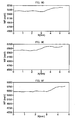
- Figs. 9A through 9F are graphs of work functions measured on three separate TiO 2 /FTO samples before ( Figs. 9A-9C ) and after ( Figs. 9D-9F ) SnO 2 coating treatment.
- the work function difference between TiO 2 and FTO is measured to be between ⁇ 400 to 700 meV, which agrees well with the reported work function number. After coating with SnO 2 , the work function difference is ⁇ 200 meV. Note that the potential value of the SnO 2 /TiO 2 /FTO surface (after coating) is similar to the value of the FTO surface (before coating).
- a tin oxide (SnO 2 ) coated titanium oxide (TiO 2 ) composite nanostructure has been provided along with a DSC device made from the SnO 2 coated TiO 2 nanostructures.
- SnO 2 tin oxide coated titanium oxide
- TiO 2 titanium oxide
- TiO 2 titanium oxide
- SnO 2 tin oxide
- a set of “ordered” structures are formed in a uniform direction.
- “ordered one-dimensional” structures are line-like structures having a high aspect ratio of length to diameter, such as a wire, tube, or rod aligned in a uniform direction. That is, a set of one-dimensional structures have center axes aligned in parallel.
- the electrical properties, especially focusing on the conduction band, are controlled by the SnO 2 .
- the SnO 2 covered TiO 2 nanostructures can be used for single junction dye-sensitized solar cells (DSCs) and tandem junction DSCs.
- DSCs single junction dye-sensitized solar cells
- tandem junction DSCs tandem junction DSCs cell
- the SnO 2 coated TiO 2 nanostructures can replace the TiO 2 nanostructure anode layer of some conventional devices.
- a DSC made from a substrate having a top surface.
- An anode layer of SnO 2 coated TiO 2 nanostructures overlies the substrate top surface.
- a dye overlies the anode layer, and a cathode overlies the dye.
- the cathode may be made from a hole conducting layer having a solid state phase or a liquid phase redox electrolyte, with a counter electrode.
- the TiO 2 nanostructures may be TiO 2 nanoparticles, TiO 2 nanowires, or TiO 2 nanotubes. In the case of TiO 2 nanowires or TiO 2 nanotubes, their center axes are perpendicular to the substrate top surface.
- the SnO 2 coating thickness is in the range of 2 to 10 nanometers (nm).
- the SnO 2 coated TiO 2 nanostructures have a dielectric layer shell, which may have a thickness in the range of 0.3 to 2 nm.
- the dielectric layer shell may be a material such as niobium oxide (NbO 3 ), aluminum oxide (Al 2 O 3 ), magnesium oxide (MgO), silicon dioxide (SiO 2 ), or TiO 2 , to name a few examples.
- the electrical connection (612) between the first PV cell (602) and the second PV cell (604) is selected from a group consisting of a series connection and a parallel connection.
- the first dye (407) has a first bandgap; and, the second dye (608) has a second bandgap, larger than, or equal to the first bandgap.
- the first anode layer (406) SnO 2 coating (304) thickness (306) is in a range of 2 to 10 nanometers (nm).
- the first anode layer (406) SnO 2 coated TiO 2 nanostructures (300) have a dielectric layer shell (308).
- the dielectric layer shell (308) has a thickness (310) in a range of 0.3 to 2 nm.
- the dielectric layer shell (308) is a material selected from a group consisting of niobium oxide (NbO 3 ), aluminum oxide (Al 2 O 3 ), magnesium oxide (MgO), silicon dioxide (SiO 2 ), and TiO 2 .
- the first cathode (408) comprises: a first material (410), selected from a group consisting of a solid state phase hole conducting layer and a liquid phase redox electrolyte, overlying the first dye (407); and, a counter electrode (412) overlying the first material (410).
- the dielectric layer shell (308) has a thickness (310) in a range of 0.3 to 2 nm.
- the dielectric layer shell (308) is a material selected from a group consisting of niobium oxide (NbO 3 ), aluminum oxide (Al 2 O 3 ), magnesium oxide (MgO), silicon dioxide (SiO 2 ), and TiO 2 .
Landscapes
- Engineering & Computer Science (AREA)
- Power Engineering (AREA)
- Microelectronics & Electronic Packaging (AREA)
- Photovoltaic Devices (AREA)
- Hybrid Cells (AREA)
Abstract

Description
- This invention generally relates to photovoltaic energy cells and, more particularly, to a dye-sensitized solar cell (DSSC or DSC) formed from a tin oxide coated titanium oxide nanostructure electrode.
-
Fig. 1 is a partial cross-sectional view of typical DSC structure (prior art). DSCs had typically exhibited low conversion efficiencies until a breakthrough in 1991 by professor Grätzel and co-workers using a nanocrystalline titanium oxide (TiO2) electrode modified with a photon absorbing dye. In modern DSC cells, the photoanode TiO2 electrode is fabricated on a transparent conducting oxide (TCO), a monolayer of absorbed dye on a TiO2 surface, a platinum (Pt) counter-electrode, and an electrolyte solution with a dissolved iodine ion/tri-iodide ion redox couple between the electrodes. The structure shown inFig. 1 has successfully demonstrated an energy conversion efficiency that exceeded 7% in 1991 (B. O'Regan and M. Gratzel, "A low cost high efficiency solar cell based on dye-sensitized colloidal Ti02 films," Nature, 353, 737-740, Oct. 24, 1991), 10% in 1993 (M.K. Nazeeruddin et al., J. Am. Chem. Soc., 115, 6382-6390, 1993), and 11.1% (L. Han et al., "High efficiency of dye-sensitized solar cell and module," IEEE 4th World Conference on Photovoltaic Energy Conversion, 179-182, 1996). - In order to sensitize the TiO2, a dye molecule is attached to the TiO2 surface. When the dye molecule absorbs a photon, an electron is excited to the lowest unoccupied molecular orbital (LUMO) and is subsequently injected into the conduction band of the TiO2. As a result of this, the dye molecule is transformed to its oxidized state. The injected electron percolates through the porous nanocrystalline structure to the TCO (negative electrode, anode) and finally through an external load to the counter electrode (positive electrode, cathode, and Pt). At the counter electrode, the electron is transferred to tri-iodide in the electrolyte to yield iodine (I3 - + 2e - → 3I-). The cycle is closed by reduction of the oxidized dye by the iodine in the electrolyte.
- In another aspect of solar cell technology, the most frequently explored strategy for achieving higher efficiency in solar cells has focused on the use of a tandem cell structure, through which individual cells can be tuned to a particular frequency of the spectrum. This allows the cells to be stacked such that layers capable of capturing shorter wavelengths are located on top, while longer wavelengths of light are allowed to pass through the top and travel to the lower layers. For DSC cells, several tandem cell concepts and structures have been proposed. One proposal suggests a random mixture of two or more dyes with different absorption spectra (molecular cocktail). So far, this approach has not led to higher efficiency cells when compared to the best (single) dye with broad absorption characteristics.
- As noted above, a DSC is typically composed of a mesoporous TiO2 electrode sensitized with a photon absorbing dye, which is in turn contacted by a redox-active hole transporting medium. Photoexcitation of the sensitizer leads to electron transfer from the excited dye to TiO2 conduction band, and the oxidized dye is regenerated via hole-transfer to the redox active medium. The photoelectron generation, charge transfer, and dye regeneration are well studied. The charge transfer from the excited dye to TiO2 conduction band depends upon the anchoring function group of the dye and the energy difference between the excited dye and the TiO2 conduction band. In principle, a more efficient electron transfer occurs for the system with a larger energy difference.
- In addition, for a dye to absorb longer wavelengths, the energy difference between the ground state (highest occupied molecular orbital, HOMO) and the excited state (lowest unoccupied molecular orbital, LUMO) must be reduced. For instance, for a dye to be able to absorb wavelengths shorter than 700 nanometers (nm), its bandgap (energy difference between HOMO and LUMO) is around 1.8 electron volts (eV). For a dye to absorb wavelengths shorter than 1050 nm, its bandgap is around 1.2 eV. When the bandgap of the dye shrinks, the LUMO level drops, and the energy difference (between the excited dye (LUMO level) and the TiO2 conduction band) decreases, leading to a decreased likelihood of charge injection.
-
Fig. 2 illustrates the band structure of various metal oxides and semiconductors (prior art). Shown are the band positions of several semiconductors in contact with an aqueous electrolyte at apH 1. The lower edge of the conduction band (top) and the upper edge of the valence band (bottom) are presented along with the bandgap in electron volts. On the right side the standard potentials of several redox couples are presented against the standard hydrogen electrode (NHE or SHE) potential. - Comparing to the TiO2 conduction band (EC), ZnO has a 0.1 - 0.2 eV lower Ec. The favorable Ec level and ease of fabricating ZnO nanostructures, makes ZnO a common replacement for TiO2 as a photoanode in DSC development. However, ZnO is very active and unstable, and the energy difference from TiO2 is too small for many applications. Other oxides, e.g., WO3 and Fe2O3 are potential candidates, but not much related development has been done on these materials. On the other hand, SnO2 has an EC of about 0.6 eV below that of TiO2. Several published papers suggest that SnO2 may be a suitable photoanode for DSC application. In addition, bulk SnO2 has a mobility of up to 240 centimeters squared per volt-seconds (cm2/V-s), which is 100 times that of TiO2. Of course, for a DSC incorporating bare SnO2 with no surface treatment, the regeneration of the oxidized photosensitizer from the hole conductor (or the redox couple) is often not sufficiently fast, and the recombination of the conduction band electrons with the oxidized photosensitizer is incomplete. However, some reports suggest that with the incorporation of thin (sub nm) interfacial layers of wide bandgap "insulating" oxides, such as MgO or Al2O3, between the SnO2 and photosensitizer, suppress the back reaction and can enable a significant enhancement in the photovoltaic conversion efficiency.
- Mesoporous SnO2 electrodes made of SnO2 nanoparticles have been described and good DSC performance was reported. Nevertheless, DSC electrodes made of one-dimensional SnO2 nanostructures, such as nanowire, nanoribbon, and nanotube have advantages, such as a faster charge transfer. Four examples of one-dimensional SnO2 nanostructures are provided below. As used herein, a "one-dimensional structure" is essentially a structure in the shape of a line, such as a wire, tube, or rod having a high aspect ratio between the length and diameter. In some aspects, the ratio is greater than 10:1.
- SnO2 nanowires can be synthesized with sizes ranging from 20 - 200 nm in diameter and lengths up to a few tens of micrometers depending on the growth conditions. In one method, the growth of nanowires follows that of a self catalytic vapor-liquid-solid (VLS) mechanism. Quartz substrates with tin metal powders are placed in the center zone of a tubular quartz reactor. The reactor is then heated to temperatures of 850 - 950°C at ambient pressure and under a continuous flow of argon. At these elevated temperatures, the metal powders melt and form a thin film on the substrates. The branching and interconnectivity of nanowires is promoted by providing Sn droplets intermittently for secondary nucleation. This is done by fluctuating the temperatures of both the Sn source and the substrate. The precursor for nanowire growth is pure Sn metal.
- SnO2 nanotubes can be synthesized by template-directed electrodeposition using nuclear track etching of polycarbonate membranes with a nominal pore diameter of 50 or 100 nm. The rated thickness and pore density are 6 µm and 6 × 10⁸ pores cm-2, respectively. One side of the polycarbonate membrane is first coated with a 500 nm thick layer of gold by sputtering to create a seed layer. The electrical contact is made to the membrane working electrode using a conductive copper tape. The resultant template is placed in an electrolyte cell, such that an area of 1 cm2 is exposed to the electrolyte. Platinum gauze is used as the counter electrode and a Ag/AgCl (3 M KCl) electrode serves as the reference electrode. Electrochemical synthesis is performed under a potentiostatic mode using a multichannel potentio/galvanostat. The electrolyte consists of 20 mM tin chloride, 0.1 M sodium nitrate, and 75 mM nitric acid in distilled (DI) water. SnO2 is deposited on the templates using a fixed potential of -0.4 V (versus Ag/AgCl) with varying deposition times. Following deposition, the gold seed layer used as the working electrode is mechanically removed and the membrane rinsed in DI water. The nanotubes are released by dissolving the polycarbonate membrane in dichloromethane. The suspension is centrifuged, the nanotubes washed three times with dichloromethane, and finally suspended in isopropanol. The resultant SnO2 nanotubes are annealed in air at 400 °C for 4 hours to investigate the effect of annealing on the crystal structure of the nanotubes.
- The experimental apparatus used for the synthesis of SnO2 nanoribbons consists of a horizontal alumina tube furnace, a rotary pump, and a gas supply. SnO or SnO2 powder is used as the source material, placed in an alumina crucible, with the crucible being located at the center of the alumina tube. Several alumina substrates are placed downstream inside the alumina tube for collecting the growth products. After evacuating the alumina tube to 2x10⁻³ Torr, thermal evaporation is conducted at 1000 °C for SnO powders, or 1350 °C for the SnO2 powders, for 2 hours under a pressure of 300 Torr and Ar gas flow rate of 50 standard cubic centimeters per minute (sccm). A white-color, fuzzy looking product is collected in a region where the temperature is in the range of 900-950 °C. Electron diffraction analysis reveals that each nanoribbon is single crystalline SnO2 without dislocation.
- In one method, a horizontal quartz tube is mounted inside a high-temperature tube furnace. A mixture of active carbon powder 1.2 grams (g) and fine SnO2 powder 5 g are placed on a quartz crucible and Si substrates (deposited with thin 5 nm Au) are placed downstream of the furnace. After the wafer is inserted into the center of the quartz tube, the quartz tube is first evacuated by a vacuum pump. Next, the furnace is rapidly heated up to 700 °C from room temperature under a N2 flow at a rate of about 100 sccm. The pressure is kept at 200 Torr and the heating lasts for 240 minutes. Subsequently, the furnace is cooled to room temperature naturally, and the products are collected on the substrates from different regions of the furnace. All these regions have the same temperature of 700 °C. It is observed that thick, white, cotton-wool-like products are deposited on the surfaces of the substrates. Scanning electron microscope (SEM) images of the resulting product indicate single crystalline SnO2 nanowires.
- Some of the previously discussed one-dimensional SnO2 nanostructures exhibit a single crystalline structure. DSC cells have been successfully fabricated with these one-dimensional nanostructures. As discussed above, thin (sub nm) interfacial layers of wide bandgap "insulating" oxides are needed to suppress the back reaction. However, there are challenges with using these one-dimensional SnO2 nanostructures; for example (1) they are random powder-like structures and (2) synthesis temperatures are very high.
- It would be advantageous to produce SnO2 as an ordered, one dimensional nanostructures using a low temperature process.
- According to one aspect of the invention, a dye-sensitized solar cell (DSC) comprises: a substrate having a top surface; an anode layer comprising tin oxide (SnO2) coated titanium oxide (TiO2) nanostructures overlying the substrate top surface; a dye overlying the anode layer; and, a cathode overlying the dye.
- According to one aspect of the invention, a tandem dye-sensitized solar cell (DSC) comprises: a first photovoltaic (PV) cell including: a first anode layer of tin oxide (SnO2) coated titanium oxide (TiO2) nanostructures; a first dye overlying the first anode layer; a first cathode overlying the first dye; a second PV cell including: a second anode layer of TiO2 nanostructures; a second dye overlying the second anode; a second cathode overlying the second dye; an electrical connection between the first PV cell and the second PV cell; and, wherein an electrode of the second PV cell, selected from a group consisting of the second anode and second cathode, is configured to initially accept incident light.
- According to one aspect of the invention, a composite nanostructure comprises: a titanium oxide (TiO2) nanostructure core; and, a tin oxide (SnO2) coating covering the core.
-
-
Fig. 1 is a partial cross-sectional view of typical DSC structure (prior art). -
Fig. 2 illustrates the band structure of various metal oxides and semiconductors (prior art). -
Figs. 3A through 3D are partial cross-sectional views of a composite nanostructure. -
Fig. 4 is a partial cross-sectional view depicting a dye-sensitized solar cell (DSC). -
Fig. 5 is a partial cross-sectional view depicting the DSC ofFig. 4 in greater detail. -
Figs. 6A through 6C are partial cross-sectional views of a tandem DSC. -
Figs. 7A and 7B respectively depict plan and partial cross-sectional views of a first step in the fabrication of SnO2 coated TiO2 nanostructures before measurement. -
Figs. 8A and 8B respectively depict plan and partial cross-sectional views of a second step in the fabrication of SnO2 coated TiO2 nanostructures. -
Figs. 9A through 9F are graphs of work functions measured on three separate TiO2/FTO samples before (Figs. 9A-9C ) and after (Figs. 9D-9F ) SnO2 coating treatment. -
Fig. 10 is a diagram depicting the band structure relationship between TiO2, SnO2, a first dye, and a second dye. -
Figs. 3A through 3D are partial cross-sectional views of a composite nanostructure. Thecomposite nanostructure 300 comprises a titanium oxide (TiO2)nanostructure core 302 and a tin oxide (SnO2) coating 304 covering thecore 302. The SnO2 coating 304 has athickness 306 in the range of 2 to 10 nanometers (nm). InFig. 3A , the TiO2 nanostructure core 302 is a nanowire morphology, inFig. 3B , the morphology is a nanotube, and inFig. 3C the morphology is a nanoparticle. - The composite nanostructure of
Fig. 3D additionally comprises adielectric layer shell 308 overlying the SnO2 coating 304. Here the TiO2 nanostructure core 302 is shown as a nanowire, but it could just as well be a nanotube or nanoparticle. Thedielectric layer shell 308 has athickness 310 in the range of 0.3 to 2 nm. Some examples of thedielectric layer shell 308 material include niobium oxide (NbO3), aluminum oxide (Al2O3), magnesium oxide (MgO), silicon dioxide (SiO2), and TiO2. Other materials, especially metal oxide materials may possibly be used. -
Fig. 4 is a partial cross-sectional view depicting a dye-sensitized solar cell (DSC). The DSC 400 comprises asubstrate 402 having atop surface 404. Ananode layer 406 comprising SnO2 coated TiO2 nanostructures, identified inFigs. 3A-3D ascomposite structures 300, overlie the substrate top surface. Thesubstrate 402 may be made from a transparent conductive oxide (TCO) material, such as In2O3-SnO2 (indium tin oxide or ITO), tin oxide (SnO2), zinc oxide (ZnO), aluminum/gallium doped zinc oxide (ZnO:Al(Ga)), a carbon nanotube layer, a graphene layer, or fluorine doped tin oxide (SnO2:F or FTO). Adye 407 overlies theanode layer 406, and acathode 408 overlies the dye. Thecathode 408 is comprised of afirst material 410, which may be a hole conducting layer having a solid state phase or a redox electrolyte having a liquid phase, overlying thedye 407. Although thedye 407 is depicted as a separate layer, it should be understood that the dye may permeate into the SnO2 coated TiO2 nanostructures of theanode layer 406. Similarly, it should be understood that thefirst material 410 may permeate into the SnO2 coated TiO2 nanostructures of theanode layer 406 and be in contact with thedye 407. - A
counter electrode 412 overlies thefirst material 410. For example, the first material may be a redox electrolyte that includes iodine and/or tri-iodine. As used herein, the orientation of the DSC 400 is relative. Therefore, the term "underlie" may alternatively be understood to mean "overlie" or in direct physical contact, depending upon the orientation of the DSC 400. - In one aspect, the
substrate 402 is formedoverlying glass 416 and acts as an external electrode. In another aspect, thecounter electrode 412 acts as an external electrode and can be made from a metal such as platinum (Pt), platinum/aluminum (Pt/Al), silver (Ag), gold (Au), or carbon. The external electrodes are configured to be connected to other DSCs or electrical circuitry (not shown) such as a DC-to-AC inverter. - As explained above in the descriptions of
Figs. 3A-3D , the TiO2 nanostructures, referred to as TiO2 nanostructure cores 302 inFigs. 3A-3D , may be TiO2 nanoparticles (Fig. 3C ), TiO2 nanowires (Fig. 3A ), or TiO2 nanotubes (Fig. 3B ). Referring still toFigs. 3A-3D , the SnO2 coating thickness 306 on the TiO2 nanostructures 302 is in the range of 2 to 10 nm. In some aspects, the TiO2 nanostructure acts as a "backbone" to make an ordered one-dimensional nanostructure. The SnO2 coating on the surface of TiO2 improves the charge transfer from the excited dye to SnO2 conduction band. - Further, as shown in
Fig. 3D , the SnO2 coated TiO2 nanostructures 300 may further comprise adielectric layer shell 308 overlying the SnO2 coating 304. Thedielectric layer shell 308 has athickness 310 in the range of 0.3 to 2 nm. Some examples of thedielectric layer shell 308 material include niobium oxide (NbO3), aluminum oxide (Al2O3), magnesium oxide (MgO), silicon dioxide (SiO2), and TiO2. Other materials, especially metal oxide materials may possibly be used. Since the SnO2 surface may exhibit high charge recombination, the thin layer of dielectric layer may be used to inhibit charge recombination. Note that thedielectric layer 308 is much thinner than the SnO2 coating 304, and it does not affect the charge transfer from theexcited dye 407 to SnO2 conduction band. -
Fig. 5 is a partial cross-sectional view depicting the DSC ofFig. 4 in greater detail. In the case where the TiO2 nanostructures 302 are TiO2 nanowires or TiO2 nanotubes, they have acenter axis 500 perpendicular to thesubstrate top surface 404. That is, the SnO2 coated TiO2 nanostructures 300 are ordered in a direction perpendicular to thesubstrate top surface 404. -
Figs. 6A through 6C are partial cross-sectional views of a tandem DSC. Thetandem DSC 600 comprises a first photovoltaic (PV)cell 602 and asecond PV cell 604. Thefirst PV cell 602 includes afirst anode layer 406 of SnO2 coated TiO2 nanostructures. The SnO2 coated TiO2 nanostructures are labeled withreference designator 300 inFig. 4 . Details of the SnO2 coated TiO2 nanostructures have been presented above in the descriptions ofFigs. 3A-3D and4 , and are not repeated here in the interest of brevity. As noted above in the description ofFig. 4 , thefirst anode layer 406 is typically formed overlying a substrate (seeFig. 4 , reference designator 402). Afirst dye 407 overlies thefirst anode layer 406, and afirst cathode 408 overlying thefirst dye 407. As noted above in the description ofFig. 4 , thefirst cathode 408 comprises afirst material 410, which may be a solid state phase hole conducting layer and or liquid phase redox electrolyte, overlying thefirst dye 407, and acounter electrode 412 overlying the first material. - The
second PV cell 604 includes asecond anode layer 606 of TiO2 nanostructures. Note: the TiO2 nanostructures that make up thesecond anode layer 606 are not coated with tin oxide. Asecond dye 608 overlies thesecond anode 606, and asecond cathode 610 overlies thesecond dye 608. Thesecond cathode 610 may be formed from one of the above-described first materials and a counter electrode. Anelectrical connection 612 exists between thefirst PV cell 602 and thesecond PV cell 604. Theelectrical connection 612 may be a parallel connection, as shown inFig. 6A , or a series connection, as described below. Either thesecond anode 606 of thesecond PV cell 604, or the second cathode 610 (as shown inFig. 6A ), is configured to initially acceptincident light 613. Typically, thefirst dye 407 has a first bandgap and thesecond dye 608 has a second bandgap, larger than, or equal to the first bandgap. -
Fig. 10 is a diagram depicting the band structure relationship between TiO2, SnO2, a first dye, and a second dye. Only the Ec is shown for TiO2 and SnO2 (refer toFig. 2 ). Note, the terms Ec and Ev are used for crystalline structures, while LUMO and HOMO are used for molecules. Conventional dye-sensitized solar cells have a dye bandgap (LUMO to HOMO) of around 1.7 eV, and can absorb wavelengths shorten than 750 nm well, using a TiO2 nanostructured anode. In order to improve absorption for longer wavelengths, the bandgap of the dye (LUMO to HOMO) must be smaller than 1.7 eV. As the bandgap gets smaller, the distance (energy drop) from the LUMO of the smaller bandgap dye to TiO2 Ec becomes smaller (ΔV3 in the figure). Further, the charge injection from the dye to Ec is easier if the energy drop is larger. For this reason, SnO2 is used in conjunction with the smaller bandgap dye. From the figure, you can see ΔV2 is larger than ΔV3, so the change injection to SnO2 is easier than injection to TiO2. - In a tandem PV cell, the light preferably initially intersects the larger bandgap material of the second PV cell (604,
Figs. 6A-6C ). Photons having less energy (longer wavelength) than the bandgap (Eg) of the second PV cell pass through, and can be absorbed by the first PV cell (602,Fig. 6A-6C ) with the smaller Eg material. - In one aspect, the series connection is made using a transparent conductive adhesive. For example, organic adhesives may be used such as: poly(3,4-ethylenedioxythiophene):poly(styrene sulfonate) (PEDOT:PSS) or similar polymers based upon the PEDOT scaffolding such as Aedotron™ and Oligotron™ (TDA Research, Inc.), polythiophene derivatives, polyaniline, polypyrrole, polyacetylene, polyphenylenevinylene, polyphenylene sulfides, etc., which may contain other additives to increase conductivity and/or adhesion properties. Further, otherwise nonconductive or low conductivity adhesive polymers may be used that are appropriately doped with metals, metal nanoparticles, carbon nanotubes, etc., in order to increase conductivity.
- Although not explicitly shown, the
second PV cell 604 may be formed on glass substrate with intervening external electrodes made from a transparent conductive oxide (TCO) layer and a metal, as is conventional. The TCO layer can be selected from the following materials: SnO2:F (FTO), In2O3-SnO2 (ITO), ZnO, ZnO:Al(Ga), carbon nanotube layer and graphene layer. -
Fig. 6B depicts thefirst anode 406 of thefirst PV cells 602 connected in series with thesecond cathode 610 of thesecond PV cell 604. In this aspect, thetandem DSC 600 is configured so that thesecond anode 606 initially acceptsincident light 613.Fig. 6C depicts thefirst cathode 408 of thefirst PV cell 602 connected in series with thesecond anode 606 of thesecond PV cell 604. In this aspect, thetandem DSC 600 is configured so that thesecond cathode 610 initially acceptsincident light 613. - It should be understood that there are a number of ways of mechanically configuring the
tandem DSC 600. The first andsecond PV cells 602/604 may be fabricated as a single module. Alternatively, the first andsecond PV cells 602/604 may be fabricated as separate modules, and connected together, mechanically and electrically, upon installation. In another aspect, the first andsecond PV cells 602/604 may be fabricated as separate modules and electrically connected at a DC-to-AC inverter. - Using SnO2 coated TiO2 nanostructures, it is possible to design a nanostructured electrode that exhibits the electrical properties of SnO2, such as the conduction band Ec and electrical conductivity, while simultaneously exhibiting the physical properties of TiO2 nanostructure, such as morphology, as well as bond and transfer characteristics. Experimental data is provided below, of coating a SnO2 layer on a planar TiO2 film for ease of characterization.
-
Figs. 7A and 7B respectively depict plan and partial cross-sectional views of a first step in the fabrication of SnO2 coated TiO2 nanostructures before measurement.Blanket TiO 2 700 was sputtered onto fluorine-doped tin oxide (FTO) 702. A masked portion ofFTO 702 was left uncoated. -
Figs. 8A and 8B respectively depict plan and partial cross-sectional views of a second step in the fabrication of SnO2 coated TiO2 nanostructures. The sample ofFigs. 7A and 7B was soaked in Tin(IV) isopropoxide and annealed to formSnO 2 800 prior to measurement. - As described by Diamant et al (Coordination Chemistry Reviews 248 (2004) 1271-1276), nanoporous TiO2 can be coated with SnO2 by dipping in a 50 mM Sn-isopropoxide solution, and then annealing at 500 °C for 30 minutes. For an initial experiment, 50 mM Tin(IV) isopropoxide in anhydrous isopropanol was prepared. Samples of sputtered/annealed TiO2 film on FTO glass were soaked for 30 seconds, air-dried, and annealed at 500 °C for 30 minutes in ambient. The SnO2 layer thickness is very thin due to short processing time (30 second), and it is difficult to accurately determine the correct thickness since the film is coated on a rough substrate (FTO glass). Kelvin probe measurements were used to determine the work function of the film before and after the SnO2 coating procedure.
- The Kelvin probe is a non-contact, vibrating capacitor instrument used to measure the work function difference between materials. The work function is indicative of surface condition and can reveal information regarding surface contamination, charging, oxidation, etc. The Kelvin probe utilizes a "calibration disk" consisting of a gold surface which is used to measure a "reference" work function Au(ref). From this reference, the following can be calculated:


where Au(theoretical) = 5.1 to 5.47eV -
Figs. 9A through 9F are graphs of work functions measured on three separate TiO2/FTO samples before (Figs. 9A-9C ) and after (Figs. 9D-9F ) SnO2 coating treatment. The work function difference, measured using the Kelvin probe, decreased to ∼200 meV (1 meV = 0.001 eV) for each sample. The work function difference between TiO2 and FTO is measured to be between ∼400 to 700 meV, which agrees well with the reported work function number. After coating with SnO2, the work function difference is ∼200 meV. Note that the potential value of the SnO2/TiO2/FTO surface (after coating) is similar to the value of the FTO surface (before coating). This observation is in accordance with expectation, as the work function of SnO2 should be similar to FTO. Interestingly, the work function of SnO2-coated FTO also increased slightly. This indicates that the coated SnO2 film is so thin so that the surface potential is affected by the film under the SnO2. - A tin oxide (SnO2) coated titanium oxide (TiO2) composite nanostructure has been provided along with a DSC device made from the SnO2 coated TiO2 nanostructures. Particular materials, device structures, and process details have been presented as examples to illustrate the invention. However, the invention is not limited to just these examples. Other variations and embodiments of the invention will occur to those skilled in the art.
- According to one aspect of the invention, disclosed herein are titanium oxide (TiO2) nanostructures covered with tin oxide (SnO2), resulting in an ordered, one-dimensional nanostructure. As used herein, a set of "ordered" structures are formed in a uniform direction. Thus, "ordered one-dimensional" structures are line-like structures having a high aspect ratio of length to diameter, such as a wire, tube, or rod aligned in a uniform direction. That is, a set of one-dimensional structures have center axes aligned in parallel. The electrical properties, especially focusing on the conduction band, are controlled by the SnO2. The SnO2 covered TiO2 nanostructures can be used for single junction dye-sensitized solar cells (DSCs) and tandem junction DSCs. In the case of tandem junction DSCs cell, the SnO2 coated TiO2 nanostructures can replace the TiO2 nanostructure anode layer of some conventional devices.
- Accordingly, a DSC is provided, made from a substrate having a top surface. An anode layer of SnO2 coated TiO2 nanostructures overlies the substrate top surface. A dye overlies the anode layer, and a cathode overlies the dye. The cathode may be made from a hole conducting layer having a solid state phase or a liquid phase redox electrolyte, with a counter electrode. The TiO2 nanostructures may be TiO2 nanoparticles, TiO2 nanowires, or TiO2 nanotubes. In the case of TiO2 nanowires or TiO2 nanotubes, their center axes are perpendicular to the substrate top surface. Regardless of the TiO2 nanostructure morphology, the SnO2 coating thickness is in the range of 2 to 10 nanometers (nm). In one aspect, the SnO2 coated TiO2 nanostructures have a dielectric layer shell, which may have a thickness in the range of 0.3 to 2 nm. The dielectric layer shell may be a material such as niobium oxide (NbO3), aluminum oxide (Al2O3), magnesium oxide (MgO), silicon dioxide (SiO2), or TiO2, to name a few examples.
- Additional details of the above-described DSC, a tandem DSC, and a composite nanostructure are provided below.
- In one aspect of the tandem DSC (600) of the invention, the electrical connection (612) between the first PV cell (602) and the second PV cell (604) is selected from a group consisting of a series connection and a parallel connection.
- In one aspect of the tandem DSC (600) of the invention, the first dye (407) has a first bandgap; and, the second dye (608) has a second bandgap, larger than, or equal to the first bandgap.
- In one aspect of the tandem DSC (600) of the invention, the first anode layer (406) SnO2 coating (304) thickness (306) is in a range of 2 to 10 nanometers (nm).
- In one aspect of the tandem DSC (600) of the invention, the first anode layer (406) SnO2 coated TiO2 nanostructures (300) have a dielectric layer shell (308).
- In one aspect of the tandem DSC (600) of the invention, the dielectric layer shell (308) has a thickness (310) in a range of 0.3 to 2 nm.
- In one aspect of the tandem DSC (600) of the invention, the dielectric layer shell (308) is a material selected from a group consisting of niobium oxide (NbO3), aluminum oxide (Al2O3), magnesium oxide (MgO), silicon dioxide (SiO2), and TiO2.
- In one aspect of the tandem DSC (600) of the invention, the first cathode (408) comprises: a first material (410), selected from a group consisting of a solid state phase hole conducting layer and a liquid phase redox electrolyte, overlying the first dye (407); and, a counter electrode (412) overlying the first material (410).
- In one aspect of the composite nanostructure (300) of the invention, the dielectric layer shell (308) has a thickness (310) in a range of 0.3 to 2 nm.
- In one aspect of the composite nanostructure (300) of the invention, the dielectric layer shell (308) is a material selected from a group consisting of niobium oxide (NbO3), aluminum oxide (Al2O3), magnesium oxide (MgO), silicon dioxide (SiO2), and TiO2.
- This application is based on a Continuation-in-part (CIP) of a patent application entitled, TANDEM DYE-SENSITIZED SOLAR CELL AND METHOD FOR MAKING SAME, invented by
Lee et al., Serial No. 12/892,779, filed September 28, 2010
Claims (15)
- A dye-sensitized solar cell (DSC) (400) comprising:a substrate (402) having a top surface (404);an anode layer (406) comprising tin oxide (SnO2) coated titanium oxide (TiO2) nanostructures (300) overlying the substrate (402) top surface (404);a dye (407) overlying the anode layer (406); and,a cathode (408) overlying the dye (407).
- The DSC (400) of claim 1 wherein the cathode (408) comprises:a first material (410), selected from a group consisting of a hole conducting layer having a solid state phase and a redox electrolyte having a liquid phase, overlying the dye (407); and,a counter electrode (412) overlying the first material (410).
- The DSC (400) of claim 1 or 2 wherein the TiO2 nanostructures (300) are selected from a group consisting of TiO2 nanoparticles, TiO2 nanowires, and TiO2 nanotubes.
- The DSC (400) of claim 1 or 2 wherein the TiO2 nanostructures (300) are selected from a group consisting of TiO2 nanowires and TiO2 nanotubes, having a center axes (500) perpendicular to the substrate (402) top surface (404).
- The DSC (400) of any one of claims 1 through 4 wherein the SnO2 coating (304) thickness (306) on the TiO2 nanostructures (300) is in a range of 2 to 10 nanometers (nm).
- The DSC (400) of any one of claims 1 through 5 wherein the SnO2 coated TiO2 nanostructures (300) have a dielectric layer shell (308).
- The DSC (400) of claim 6 wherein the dielectric layer shell (308) has a thickness (310) in a range of 0.3 to 2 nm.
- The DSC (400) of claim 6 wherein the dielectric layer shell (308) is a material selected from a group consisting of niobium oxide (NbO3), aluminum oxide (Al2O3), magnesium oxide (MgO), silicon dioxide (SiO2), and TiO2.
- A tandem dye-sensitized solar cell (DSC) (600) comprising:a first photovoltaic (PV) cell (602) including:a first anode layer (406) of tin oxide (SnO2) coated titanium oxide (TiO2) nanostructures (300);a first dye (407) overlying the first anode layer (406);a first cathode (408) overlying the first dye (407);a second PV cell (604) including:a second anode layer (606) of TiO2 nanostructures;a second dye (608) overlying the second anode (606);a second cathode (610) overlying the second dye (608);an electrical connection (612) between the first PV cell (602) and the second PV cell (604); and,wherein an electrode of the second PV cell (604), selected from a group consisting of the second anode (606) and second cathode (610), is configured to initially accept incident light (613).
- The tandem DSC (600) of claim 9 wherein the electrical connection (612) between the first PV cell (602) and the second PV cell (604) is selected from a group consisting of a series connection and a parallel connection.
- The tandem DSC (600) of claim 9 or 10 wherein the first dye (407) has a first bandgap; and,
wherein the second dye (608) has a second bandgap, larger than, or equal to the first bandgap. - A composite nanostructure (300) comprising:a titanium oxide (TiO2) nanostructure core (302); and,a tin oxide (SnO2) coating (304) covering the core (302).
- The composite nanostructure (300) of claim 12 wherein the Sn02 coating (304) thickness (306) is in a range of 2 to 10 nanometers (nm).
- The composite nanostructure (300) of claim 12 or 13 further comprising:a dielectric layer shell (308) overlying the SnO2 coating (304).
- The composite nanostructure (300) of any one of claims 12 through 14 wherein the TiO2 nanostructure core (302) is a morphology selected from a group consisting of TiO2 nanoparticles, TiO2 nanowires, and TiO2 nanotubes.
Applications Claiming Priority (1)
| Application Number | Priority Date | Filing Date | Title |
|---|---|---|---|
| US14/012,159 US20130340825A1 (en) | 2010-09-28 | 2013-08-28 | Dye-Sensitized Solar Cell with Ordered Tin Oxide Composite Nanostructure Electrodes |
Publications (1)
| Publication Number | Publication Date |
|---|---|
| EP2843674A1 true EP2843674A1 (en) | 2015-03-04 |
Family
ID=51421798
Family Applications (1)
| Application Number | Title | Priority Date | Filing Date |
|---|---|---|---|
| EP14002948.9A Withdrawn EP2843674A1 (en) | 2013-08-28 | 2014-08-25 | Dye-sensitized solar cell, tandem dye-sensitized solar cell, and composite nanostructure |
Country Status (2)
| Country | Link |
|---|---|
| EP (1) | EP2843674A1 (en) |
| JP (1) | JP2015079939A (en) |
Cited By (1)
| Publication number | Priority date | Publication date | Assignee | Title |
|---|---|---|---|---|
| CN110970566A (en) * | 2018-09-29 | 2020-04-07 | Tcl集团股份有限公司 | Core-shell nano material, preparation method thereof and quantum dot light-emitting diode |
Families Citing this family (1)
| Publication number | Priority date | Publication date | Assignee | Title |
|---|---|---|---|---|
| KR101828943B1 (en) * | 2015-10-30 | 2018-02-14 | 재단법인 대구경북과학기술원 | Perovskite solar cells comprising metal oxide nanofiber, nanorod and coating layer as photoelectrode, and the preparation method thereof |
Citations (3)
| Publication number | Priority date | Publication date | Assignee | Title |
|---|---|---|---|---|
| US20070062576A1 (en) * | 2003-09-05 | 2007-03-22 | Michael Duerr | Tandem dye-sensitised solar cell and method of its production |
| US20120073635A1 (en) * | 2010-09-28 | 2012-03-29 | Jong-Jan Lee | Tandem Dye-Sensitized Solar Cell and Method for Making Same |
| US20120199189A1 (en) * | 2009-04-09 | 2012-08-09 | The Regents Of The University Of California | Three dimensional dye-sensitized solar cells with nanoscale architectures |
Family Cites Families (4)
| Publication number | Priority date | Publication date | Assignee | Title |
|---|---|---|---|---|
| JPH10290018A (en) * | 1997-04-11 | 1998-10-27 | Fuji Photo Film Co Ltd | Semiconductor for photoelectric conversion material and chemical battery using the same |
| JP4169140B2 (en) * | 2000-10-02 | 2008-10-22 | 日揮触媒化成株式会社 | Novel metal oxide particles and uses thereof |
| JP2010265236A (en) * | 2009-05-18 | 2010-11-25 | Sumitomo Chemical Co Ltd | Silyl-containing thiazolium iodide or silyloxazolium iodide and use thereof |
| JP6198407B2 (en) * | 2013-02-27 | 2017-09-20 | 大阪瓦斯株式会社 | Paste composition for photoelectric conversion element, and electrode and photoelectric conversion element for photoelectric conversion element using the same |
-
2014
- 2014-08-21 JP JP2014168787A patent/JP2015079939A/en active Pending
- 2014-08-25 EP EP14002948.9A patent/EP2843674A1/en not_active Withdrawn
Patent Citations (3)
| Publication number | Priority date | Publication date | Assignee | Title |
|---|---|---|---|---|
| US20070062576A1 (en) * | 2003-09-05 | 2007-03-22 | Michael Duerr | Tandem dye-sensitised solar cell and method of its production |
| US20120199189A1 (en) * | 2009-04-09 | 2012-08-09 | The Regents Of The University Of California | Three dimensional dye-sensitized solar cells with nanoscale architectures |
| US20120073635A1 (en) * | 2010-09-28 | 2012-03-29 | Jong-Jan Lee | Tandem Dye-Sensitized Solar Cell and Method for Making Same |
Non-Patent Citations (6)
| Title |
|---|
| B. O'REGAN; M. GRATZEL: "A low cost high efficiency solar cell based on dye-sensitized colloidal Ti02 films", NATURE, vol. 353, 24 October 1991 (1991-10-24), pages 737 - 740 |
| DIAMANT ET AL., COORDINATION CHEMISTRY REVIEWS, vol. 248, 2004, pages 1271 - 1276 |
| DIAMANT Y ET AL LEVASON BILL HECTOR ANDREW L: "Core-shell nanoporous electrode for dye sensitized solar cells: the effect of shell characteristics on the electronic properties of the electrode", COORDINATION CHEMISTRY REVIEWS, ELSEVIER SCIENCE, AMSTERDAM, NL, vol. 248, no. 13-14, 1 July 2004 (2004-07-01), pages 1271 - 1276, XP004578918, ISSN: 0010-8545, DOI: 10.1016/J.CCR.2004.03.003 * |
| HUANG J ET AL: "Fabrication of ZnO/Al2O3 core-shell nanostructures and crystalline Al2O3 nanotube", APPLIED SURFACE SCIENCE, ELSEVIER, AMSTERDAM, NL, vol. 254, no. 18, 15 July 2008 (2008-07-15), pages 5917 - 5920, XP022695097, ISSN: 0169-4332, [retrieved on 20080401], DOI: 10.1016/J.APSUSC.2008.03.150 * |
| L. HAN ET AL.: "High efficiency of dye-sensitized solar cell and module", IEEE 4TH WORLD CONFERENCE ON PHOTOVOLTAIC ENERGY CONVERSION, 1996, pages 179 - 182 |
| M.K. NAZEERUDDIN ET AL., J. AM. CHEM. SOC., vol. 115, 1993, pages 6382 - 6390 |
Cited By (1)
| Publication number | Priority date | Publication date | Assignee | Title |
|---|---|---|---|---|
| CN110970566A (en) * | 2018-09-29 | 2020-04-07 | Tcl集团股份有限公司 | Core-shell nano material, preparation method thereof and quantum dot light-emitting diode |
Also Published As
| Publication number | Publication date |
|---|---|
| JP2015079939A (en) | 2015-04-23 |
Similar Documents
| Publication | Publication Date | Title |
|---|---|---|
| Tétreault et al. | Novel nanostructures for next generation dye-sensitized solar cells | |
| Kang et al. | Surface modification of stretched TiO2 nanotubes for solid-state dye-sensitized solar cells | |
| Wang et al. | Significant enhancement of power conversion efficiency for dye sensitized solar cell using 1D/3D network nanostructures as photoanodes | |
| Grimes | Synthesis and application of highly ordered arrays of TiO 2 nanotubes | |
| Park et al. | Growth, detachment and transfer of highly-ordered TiO 2 nanotube arrays: use in dye-sensitized solar cells | |
| Xu et al. | Ordered TiO2 nanotube arrays on transparent conductive oxide for dye-sensitized solar cells | |
| Balasingam et al. | Metal substrate based electrodes for flexible dye-sensitized solar cells: fabrication methods, progress and challenges | |
| Xu et al. | Application of ZnO micro-flowers as scattering layer for ZnO-based dye-sensitized solar cells with enhanced conversion efficiency | |
| Kim et al. | General strategy for fabricating transparent TiO2 nanotube arrays for dye-sensitized photoelectrodes: illumination geometry and transport properties | |
| Cui et al. | Improved efficient perovskite solar cells based on Ta-doped TiO 2 nanorod arrays | |
| Yang et al. | Carrier transport in dye-sensitized solar cells using single crystalline TiO2 nanorods grown by a microwave-assisted hydrothermal reaction | |
| Guo et al. | Hierarchical TiO2 submicrorods improve the photovoltaic performance of dye-sensitized solar cells | |
| Zhou et al. | Effect of highly ordered single-crystalline TiO2 nanowire length on the photovoltaic performance of dye-sensitized solar cells | |
| Xin et al. | Dye-sensitized solar cells based on a nanoparticle/nanotube bilayer structure and their equivalent circuit analysis | |
| Nunes et al. | Nb2O5 dye-sensitized solar cells | |
| Momeni | Dye-sensitized solar cells based on Cr-doped TiO2 nanotube photoanodes | |
| Liu et al. | Enhanced photovoltaic performance of fully flexible dye-sensitized solar cells based on the Nb2O5 coated hierarchical TiO2 nanowire-nanosheet arrays | |
| Sahu et al. | Synthesis and application of core-shell Au–TiO2 nanowire photoanode materials for dye sensitized solar cells | |
| Zhou et al. | Enhanced dye-sensitized solar cells performance using anatase TiO 2 mesocrystals with the Wulff construction of nearly 100% exposed {101} facets as effective light scattering layer | |
| Wijeratne et al. | Aspect-ratio dependent electron transport and recombination in dye-sensitized solar cells fabricated with one-dimensional ZnO nanostructures | |
| Chai et al. | High-performance flexible dye-sensitized solar cells by using hierarchical anatase TiO 2 nanowire arrays | |
| KR101453605B1 (en) | Facile fabrication of aligned doubly open-ended TiO2 nanotubes, via a selective etching process, for use in front-illuminated dye sensitized solar cells | |
| Weickert et al. | Controlled growth of TiO2 nanotubes on conducting glass | |
| US20130340825A1 (en) | Dye-Sensitized Solar Cell with Ordered Tin Oxide Composite Nanostructure Electrodes | |
| Javed et al. | Anatase TiO2 nanotubes as photoanode for dye-sensitized solar cells |
Legal Events
| Date | Code | Title | Description |
|---|---|---|---|
| 17P | Request for examination filed |
Effective date: 20140825 |
|
| AK | Designated contracting states |
Kind code of ref document: A1 Designated state(s): AL AT BE BG CH CY CZ DE DK EE ES FI FR GB GR HR HU IE IS IT LI LT LU LV MC MK MT NL NO PL PT RO RS SE SI SK SM TR |
|
| AX | Request for extension of the european patent |
Extension state: BA ME |
|
| PUAI | Public reference made under article 153(3) epc to a published international application that has entered the european phase |
Free format text: ORIGINAL CODE: 0009012 |
|
| R17P | Request for examination filed (corrected) |
Effective date: 20150724 |
|
| RBV | Designated contracting states (corrected) |
Designated state(s): AL AT BE BG CH CY CZ DE DK EE ES FI FR GB GR HR HU IE IS IT LI LT LU LV MC MK MT NL NO PL PT RO RS SE SI SK SM TR |
|
| STAA | Information on the status of an ep patent application or granted ep patent |
Free format text: STATUS: THE APPLICATION HAS BEEN WITHDRAWN |
|
| 18W | Application withdrawn |
Effective date: 20160407 |