EP2840698A1 - Power converter circuit - Google Patents
Power converter circuit Download PDFInfo
- Publication number
- EP2840698A1 EP2840698A1 EP13778128.2A EP13778128A EP2840698A1 EP 2840698 A1 EP2840698 A1 EP 2840698A1 EP 13778128 A EP13778128 A EP 13778128A EP 2840698 A1 EP2840698 A1 EP 2840698A1
- Authority
- EP
- European Patent Office
- Prior art keywords
- switching
- switching elements
- switching element
- power
- subjected
- Prior art date
- Legal status (The legal status is an assumption and is not a legal conclusion. Google has not performed a legal analysis and makes no representation as to the accuracy of the status listed.)
- Withdrawn
Links
Images


Classifications
-
- H—ELECTRICITY
- H02—GENERATION; CONVERSION OR DISTRIBUTION OF ELECTRIC POWER
- H02M—APPARATUS FOR CONVERSION BETWEEN AC AND AC, BETWEEN AC AND DC, OR BETWEEN DC AND DC, AND FOR USE WITH MAINS OR SIMILAR POWER SUPPLY SYSTEMS; CONVERSION OF DC OR AC INPUT POWER INTO SURGE OUTPUT POWER; CONTROL OR REGULATION THEREOF
- H02M7/00—Conversion of AC power input into DC power output; Conversion of DC power input into AC power output
- H02M7/42—Conversion of DC power input into AC power output without possibility of reversal
- H02M7/44—Conversion of DC power input into AC power output without possibility of reversal by static converters
- H02M7/48—Conversion of DC power input into AC power output without possibility of reversal by static converters using discharge tubes with control electrode or semiconductor devices with control electrode
- H02M7/53—Conversion of DC power input into AC power output without possibility of reversal by static converters using discharge tubes with control electrode or semiconductor devices with control electrode using devices of a triode or transistor type requiring continuous application of a control signal
- H02M7/537—Conversion of DC power input into AC power output without possibility of reversal by static converters using discharge tubes with control electrode or semiconductor devices with control electrode using devices of a triode or transistor type requiring continuous application of a control signal using semiconductor devices only, e.g. single switched pulse inverters
- H02M7/5387—Conversion of DC power input into AC power output without possibility of reversal by static converters using discharge tubes with control electrode or semiconductor devices with control electrode using devices of a triode or transistor type requiring continuous application of a control signal using semiconductor devices only, e.g. single switched pulse inverters in a bridge configuration
- H02M7/53871—Conversion of DC power input into AC power output without possibility of reversal by static converters using discharge tubes with control electrode or semiconductor devices with control electrode using devices of a triode or transistor type requiring continuous application of a control signal using semiconductor devices only, e.g. single switched pulse inverters in a bridge configuration with automatic control of output voltage or current
-
- H—ELECTRICITY
- H02—GENERATION; CONVERSION OR DISTRIBUTION OF ELECTRIC POWER
- H02M—APPARATUS FOR CONVERSION BETWEEN AC AND AC, BETWEEN AC AND DC, OR BETWEEN DC AND DC, AND FOR USE WITH MAINS OR SIMILAR POWER SUPPLY SYSTEMS; CONVERSION OF DC OR AC INPUT POWER INTO SURGE OUTPUT POWER; CONTROL OR REGULATION THEREOF
- H02M7/00—Conversion of AC power input into DC power output; Conversion of DC power input into AC power output
- H02M7/42—Conversion of DC power input into AC power output without possibility of reversal
- H02M7/44—Conversion of DC power input into AC power output without possibility of reversal by static converters
- H02M7/48—Conversion of DC power input into AC power output without possibility of reversal by static converters using discharge tubes with control electrode or semiconductor devices with control electrode
- H02M7/53—Conversion of DC power input into AC power output without possibility of reversal by static converters using discharge tubes with control electrode or semiconductor devices with control electrode using devices of a triode or transistor type requiring continuous application of a control signal
- H02M7/537—Conversion of DC power input into AC power output without possibility of reversal by static converters using discharge tubes with control electrode or semiconductor devices with control electrode using devices of a triode or transistor type requiring continuous application of a control signal using semiconductor devices only, e.g. single switched pulse inverters
- H02M7/538—Conversion of DC power input into AC power output without possibility of reversal by static converters using discharge tubes with control electrode or semiconductor devices with control electrode using devices of a triode or transistor type requiring continuous application of a control signal using semiconductor devices only, e.g. single switched pulse inverters in a push-pull configuration
-
- H—ELECTRICITY
- H02—GENERATION; CONVERSION OR DISTRIBUTION OF ELECTRIC POWER
- H02M—APPARATUS FOR CONVERSION BETWEEN AC AND AC, BETWEEN AC AND DC, OR BETWEEN DC AND DC, AND FOR USE WITH MAINS OR SIMILAR POWER SUPPLY SYSTEMS; CONVERSION OF DC OR AC INPUT POWER INTO SURGE OUTPUT POWER; CONTROL OR REGULATION THEREOF
- H02M7/00—Conversion of AC power input into DC power output; Conversion of DC power input into AC power output
- H02M7/42—Conversion of DC power input into AC power output without possibility of reversal
- H02M7/44—Conversion of DC power input into AC power output without possibility of reversal by static converters
- H02M7/48—Conversion of DC power input into AC power output without possibility of reversal by static converters using discharge tubes with control electrode or semiconductor devices with control electrode
- H02M7/53—Conversion of DC power input into AC power output without possibility of reversal by static converters using discharge tubes with control electrode or semiconductor devices with control electrode using devices of a triode or transistor type requiring continuous application of a control signal
- H02M7/537—Conversion of DC power input into AC power output without possibility of reversal by static converters using discharge tubes with control electrode or semiconductor devices with control electrode using devices of a triode or transistor type requiring continuous application of a control signal using semiconductor devices only, e.g. single switched pulse inverters
- H02M7/5387—Conversion of DC power input into AC power output without possibility of reversal by static converters using discharge tubes with control electrode or semiconductor devices with control electrode using devices of a triode or transistor type requiring continuous application of a control signal using semiconductor devices only, e.g. single switched pulse inverters in a bridge configuration
Definitions
- the present invention relates to a bridge power inverter circuit which converts a DC power into an AC power.
- Non Patent Literature 1 discloses single- and three-phase inverters.
- a single-phase bridge inverter comprises first and second switching elements sequentially connected in series between input terminals on higher and lower voltage sides and third and fourth switching elements sequentially connected in series between the input terminals on the higher and lower voltage sides.
- the single-phase bridge inverter By alternately turning on a set of the first and fourth switching elements and a set of the second and third switching terminals, the single-phase bridge inverter generates a single-phase AC power between an intermediate node of the first and second switching elements and an intermediate node of the third and fourth switching elements (e.g., Figs. 6 and 9).
- a three-phase bridge inverter comprises first and second switching elements sequentially connected in series between input terminals on higher and lower voltage sides, third and fourth switching elements sequentially connected in series between the input terminals on the higher and lower voltage sides, and fifth and sixth switching elements sequentially connected in series between the input terminals on the higher and lower voltage sides.
- the three-phase bridge inverter By periodically turning on a set of the first and fourth switching elements, a set of the third and sixth switching elements, and a set of the fifth and second switching elements with a phase difference of a 1/3 cycle therebetween, the three-phase bridge inverter generates a three-phase AC power among an intermediate node of the first and second switching elements, an intermediate node of the third and fourth switching elements, and an intermediate node of the fifth and sixth switching elements (e.g., Figs. 7 and 10).
- Non Patent Literature 1 also discloses a bridge inverter which performs switching control by using a pulse width modulation (PWM) scheme during a period when the switching elements in each set are on (e.g., Fig. 13).
- PWM pulse width modulation
- Non Patent Literature 1 IMAI Koji, Power Electronics Handbook (R & D Planning Co., Ltd., February, 2002), p. 328-337
- This kind of bridge power inverter circuit necessitates four and six switching elements in single- and three-phase types, respectively.
- Such a bridge power inverter circuit performs switching control of all the switching elements at the same frequency. This makes it necessary for all the switching elements to use switching elements which can operate at relatively high speed, whereby lower cost is hard to attain.
- the power inverter circuit in accordance with the present invention is a bridge power inverter circuit comprising first and second switching elements, sequentially connected in series between input terminals on higher and lower voltage sides, having an intermediate node connected to a first output terminal; and third and fourth switching elements, sequentially connected in series between the input terminals on the higher and lower voltage sides, having an intermediate node connected to a second output terminal; the power inverter circuit alternatively turning on a set of the first and fourth switching elements and a set of the second and third switching elements so as to convert a DC power fed between the input terminals on the higher and lower voltage sides into an AC power between the first and second output terminals; wherein one of the sets of the first and third switching elements and the second and fourth switching elements is subjected to switching control at a frequency higher than that of the other.
- the power inverter circuit can use switching elements which operate at relatively low speed and are less expensive as the switching elements in the other set. Therefore, this power inverter circuit can achieve lower cost.
- a CMOSFET Complementary Metal Oxide Semiconductor Field Effect Transistor
- a PMOSFET P-channel Metal Oxide Semiconductor Field Effect Transistor
- an NMOSFET N-channel Metal Oxide Semiconductor Field Effect Transistor
- the CMOSFET is advantageous in that it is easier to be driven by a clock signal, but is disadvantageous in that the PMOSFET tends to exhibit an operating speed lower than that of the NMOSFET, thereby making it hard to attain higher speed in switching control.
- the set of the second and fourth switching elements be subjected to switching control at a frequency higher than that of the set of the first and third switching elements.
- the second and fourth switching elements on the lower arm side are subjected to switching control at a frequency higher than that of the first and third switching elements, which is suitable when using the CMOSFET as a switching element, whereby both of rapidness in switching control and easiness in driving the switching element can be obtained at the same time.
- the first switching element is turned on while the fourth switching element is subjected to switching control using a pulse width modulation scheme in a half-cycle period of the AC power when the first and fourth switching elements are on, and the third switching element is turned on while the second switching element is subjected to switching control using a pulse width modulation scheme in the other half-cycle period of the AC power when the second and third switching elements are on.
- the first switching element is subjected to switching control using a pulse width modulation scheme while the fourth switching element is subjected to switching control using a pulse width modulation scheme at a frequency at least twice as high as the switching frequency of the first switching element in a half-cycle period of the AC power when the first and fourth switching elements are on
- the third switching element is subjected to switching control using a pulse width modulation scheme while the second switching element is subjected to switching control using a pulse width modulation scheme at a frequency at least twice as high as the switching frequency of the third switching element in the other half-cycle period of the AC power when the second and third switching elements are on.
- the first to fourth switching elements are subjected to switching control so as to generate a single-phase AC power between the first and second output terminals. This makes it possible to achieve a low-cost, full-bridge single-phase inverter circuit.
- the power inverter circuit further comprises fifth and sixth switching elements, sequentially connected in series between the input terminals on the higher and lower voltage sides, having an intermediate node connected to a third output terminal; wherein the first to sixth switching elements are subjected to switching control such that one of sets of the first, third, and fifth switching elements and the second, fourth, and sixth switching elements is subjected to switching control at a frequency higher than that of the other so as to generate a three-phase AC power among the first to third output terminals.
- the present invention can achieve lower cost in bridge power inverter circuits.
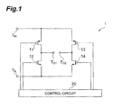
- Fig. 1 is a circuit diagram illustrating the inverter in accordance with the first embodiment of the present invention.
- the inverter (power inverter circuit) 1 of the first embodiment is a single-phase full-bridge inverter.
- the inverter 1 converts a DC power fed between a higher-voltage-side input terminal T IH and a lower-voltage-side input terminal T IL into a single-phase AC power between first and second output terminals T O1 , T O2 .
- the inverter 1 comprises first to fourth switching elements 11 to 14 and a control circuit 20.
- the first and second switching elements 11, 12 are sequentially connected in series between the higher- and lower-voltage-side input terminals T IH , T IL , while their intermediate node is connected to the first output terminal T O1 .
- the first switching element 11 on the upper arm side is a PMOSFET
- the second switching element 12 on the lower arm side is an NMOSFET.
- the first switching element 11 has a source terminal connected to the higher-voltage-side input terminal T IH and a drain terminal connected to a drain terminal of the second switching element 12.
- the second switching element 12 has a source terminal connected to the lower-voltage-side input terminal T IL .
- the drain terminals of the first and second switching elements 11, 12 are connected to the first output terminal T O1 .
- the first and second switching elements 11, 12 have gate terminals connected to the control circuit 20.
- the third and fourth switching elements 13, 14 are sequentially connected in series between the higher- and lower-voltage-side input terminals T IH , T IL , while their intermediate node is connected to the second output terminal T O2 .
- the third switching element 13 on the upper arm side is a PMOSFET
- the fourth switching element 14 on the lower arm side is an NMOSFET.
- the third switching element 13 has a source terminal connected to the higher-voltage-side input terminal T IH and a drain terminal connected to a drain terminal of the fourth switching element 14.
- the fourth switching element 14 has a source terminal connected to the lower-voltage-side input terminal T IL .
- the drain terminals of the third and fourth switching elements 13, 14 are connected to the second output terminal T O2 .
- the third and fourth switching elements 13, 14 have gate terminals connected to the control circuit 20.
- the control circuit 20 performs switching control of the first to fourth switching elements 11 to 14. Specifically, the control circuit 20 alternately turns on a set of the first and fourth switching elements 11, 14 and a set of the second and third switching elements 12, 13, so as to convert a DC current fed between the higher- and lower-voltage-side input terminals T IH , T IL into a single-phase AC power between the first and second output terminals T O1 , T O2 .
- the control circuit 20 turns on the first switching element 11, while subjecting the fourth switching element 14 to switching control using a pulse width modulation (PWM) scheme.
- PWM pulse width modulation
- control circuit 20 subjects the first and third switching elements 11, 13 on the upper arm side to switching control at the frequency of the output AC power and the second and fourth switching elements 12, 14 on the lower arm side to switching control at a frequency higher than that of the first and third switching elements 11, 13 by using the PWM scheme.
- the first and third switching elements 11, 13 are controlled such as to be alternately turned on/off at a low speed (e.g., at a frequency of 60 Hz).
- the fourth switching element 14 is subjected to PWM control at a high speed (e.g., at a frequency of 120 Hz) during a period when the first switching element 11 is on
- the second switching element 12 is subjected to PWM control at a high speed (e.g., at a frequency of 120 Hz) during a period when the third switching element 13 is on.
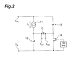
- Fig. 2 is a diagram illustrating an equivalent circuit of the inverter 1 during a period when the first switching element 11 is on
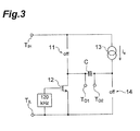
- Fig. 3 is a diagram illustrating an equivalent circuit of the inverter 1 during a period when the third switching element 13 is on.
- a smoothing capacitor (capacity value C) is supposed to be connected between the first and second output terminals T O1 , T O2 .
- a resistance load (resistance value R) is assumed to be connected between the first and second output terminals T O1 , T O2 .
- Fig. 4 is a diagram illustrating the output voltage of the inverter 1 during the period when the first switching element 11 is on. Using a time at which the fourth switching element 14 switches from off to on as the origin, the off and on times are defined as t 1 and t 2 , respectively, in Fig. 4 . That is, one cycle of on-off switching is t 1 +t 2 .
- Fig. 5 is a diagram illustrating the output voltage of the inverter 1. Fig. 5 also illustrates the on and off states of the first to fourth switching elements 11 to 14.
- the second and third switching elements 12, 13 are held in the off state as illustrated in Figs. 2 and 5 .
- the fourth switching element 14 is subjected to PWM control at 120 kHz, for example.
- the output voltage v(t) illustrated in Fig. 4 is determined from the above-mentioned expressions (9), (10), and (11).
- the first and fourth switching elements 11, 14 are held in the off state as illustrated in Figs. 3 and 5 .
- the second switching element 12 is subjected to PWM control at 120 kHz, for example.
- the output voltage waveform during the period when the third switching element 13 is on has a polarity opposite to that of the above-mentioned period when the first switching element 11 is on.
- the inverter 1 of the first embodiment can use switching elements which operate at relatively low speed and are less expensive as the first and third switching elements 11, 13 on the upper arm side.
- As drive circuits for the first and third switching elements 11, 13 on the upper arm side an inexpensive structure with relatively low operating speed can be used. Therefore, the inverter 1 of the first embodiment can achieve lower cost.
- a CMOSFET as a switching element in a bridge circuit is advantageous in that it is easily driven by a clock signal.
- a PMOSFET on the upper arm side is problematic in that it tends to exhibit an operating speed lower than that of an NMOSFET on the lower arm side, thereby making it hard to attain higher speed in switching control using a PWM scheme.
- the switching element on the upper arm side may also be constituted by an NMOSFET.
- This is advantageous in that higher speed in switching control by the NMOSFET is easier to achieve.
- an insulating device such as a photocoupler is necessary in a drive circuit for the NMOSFET on the upper arm side, which impairs easiness in driving the switching element and makes it hard to achieve lower cost.
- the inverter 1 of the first embodiment is suitable when using a CMOSFET as a switching element and can achieve higher speed in switching control, easiness in driving the switching element, and lower cost.
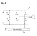
- Fig. 6 is a circuit diagram illustrating the inverter in accordance with the second embodiment of the present invention.
- the inverter (power inverter circuit) 1A of the second embodiment is a three-phase bridge inverter.
- the inverter 1A converts a DC power fed between a higher-voltage-side input terminal T IH and a lower-voltage-side input terminal T IL into a three-phase AC power among first to third output terminals T O1 , T O2 , T O3 .
- the inverter 1A differs from the inverter 1 of the first embodiment in that it further comprises fifth and sixth switching elements 15, 16 and a control circuit 20A in place of the control circuit 20.
- the fifth and sixth switching elements 15, 16 are sequentially connected in series between the higher- and lower-voltage-side input terminals T IH , T IL , while their intermediate node is connected to the first output terminal T O3 .
- the fifth switching element 15 on the upper arm side is a PMOSFET
- the sixth switching element 16 on the lower arm side is an NMOSFET.
- the fifth switching element 15 has a source terminal connected to the higher-voltage-side input terminals T IH and a drain terminal connected to a drain terminal of the sixth switching element 16.
- the sixth switching element 16 has a source terminal connected to the lower-voltage-side input terminals T IL .
- the drain terminals of the fifth and sixth switching elements 15, 16 are connected to the sixth output terminal T O3 .
- the fifth and sixth switching elements 15, 16 have gate terminals connected to the control circuit 20A.
- the control circuit 20A performs switching control of the first to sixth switching elements 11 to 16. For example, the control circuit 20A alternately turns on a set of the first and fourth switching elements 11, 14, a set of the third and sixth switching elements 13, 16, and a set of the fifth and second switching elements 15, 12 with a phase difference of a 1/3 cycle therebetween, so as to convert a DC current fed between the higher- and lower-voltage-side input terminals T IH , T IL into a three-phase AC power among the first to third output terminals T O1 to T O3 .
- the control circuit 20A turns on the first switching element 11, while subjecting the fourth switching element 14 to switching control using a PWM scheme.
- the control circuit 20A turns on the third switching element 13, while subjecting the sixth switching element 16 to switching control using the PWM scheme.
- the control circuit 20A turns on the fifth switching element 15, while subjecting the second switching element 12 to switching control using the PWM scheme.
- control circuit 20A subjects the first, third, and fifth switching elements 11, 13, 15 on the upper arm side to switching control at the frequency of the output AC power and the second, fourth, and sixth switching elements 12, 14, 16 on the lower arm side to switching control at a frequency higher than that of the first, third, and fifth switching elements 11, 13, 15 by using the PWM scheme.
- the inverter 1A of the second embodiment can also use switching elements which operate at relatively low speed and are less expensive as the first, third, and fifth switching elements 11, 13, 15 on the upper arm side.
- As drive circuits for the first, third, and fifth switching elements 11, 13, 15 on the upper arm side an inexpensive structure with relatively low operating speed can be used. Therefore, the inverter 1A of the second embodiment can also achieve lower cost.
- the present invention can be modified in various ways without being restricted to the above-mentioned embodiments.
- a CMOSFET is used as a switching element
- a PMOSFET and an NMOSFET are used as switching elements on the upper and lower arm sides, respectively
- the combination of switching elements on the upper and lower arm sides is not limited to that in the embodiments.
- a switching element which has a conductivity type different from that of the switching element on the lower arm side and an operating speed lower than that of the switching element on the lower arm side may be used as a switching element on the upper arm side.
- N- and P-channel transistors may be used as switching elements on the lower and upper arm sides, respectively.
- a switching element which has a structure different from that of the switching element on the lower arm side and an operating speed lower than that of the switching element on the lower arm side may be used as a switching element on the upper arm side.
- a switching element which can operate at relatively high speed may be selected from a group constituted by FETs, IGBTs, bipolar transistors, thyristors, and the like and used as a switching element on the lower arm side
- a switching element having relatively low operating speed and a structure different from that of the switching element on the lower arm side may be selected from a group constituted by FETs, IGBTs, bipolar transistors, thyristors, and the like and used as a switching element on the upper arm side.
- a switching element which has a device different from that of the switching element on the lower arm side and an operating speed lower than that of the switching element on the lower arm side may be used as a switching element on the upper arm side.
- a switching element constituted by an SiC device which can operate at relatively high speed may be used as a switching element on the lower arm side, while a switching element constituted by an SiC device having relatively low operating speed may be used as a switching element on the upper arm side.
- the switching elements on the lower arm side are subjected to switching control at a frequency higher than that of the switching elements on the upper arm side in the embodiments, the switching elements on the upper arm side may be subjected to switching control at a frequency higher than that of the switching elements on the lower arm side.
- the switching elements on the upper arm side (i.e., lower speed side), which are not subjected to switching control using the PWM scheme, may be subjected to switching control using the PWM scheme in a half-cycle period of the AC power when the switching elements on the upper arm side are on.
- the switching frequency on the lower arm side is preferably at least twice as high as the switching frequency of the switching elements on the upper arm side.
- the switching control on the lower arm side and that on the upper arm side are synchronized with each other.
- the present invention can be employed for lowering the cost of power inverter circuits.
Landscapes
- Engineering & Computer Science (AREA)
- Power Engineering (AREA)
- Inverter Devices (AREA)
Abstract
Description
- The present invention relates to a bridge power inverter circuit which converts a DC power into an AC power.
- As a power inverter circuit which converts a DC power into an AC power, bridge inverters have been known widely. As bridge inverters of this kind,
Non Patent Literature 1 discloses single- and three-phase inverters. - A single-phase bridge inverter comprises first and second switching elements sequentially connected in series between input terminals on higher and lower voltage sides and third and fourth switching elements sequentially connected in series between the input terminals on the higher and lower voltage sides. By alternately turning on a set of the first and fourth switching elements and a set of the second and third switching terminals, the single-phase bridge inverter generates a single-phase AC power between an intermediate node of the first and second switching elements and an intermediate node of the third and fourth switching elements (e.g.,
Figs. 6 and 9). - On the other hand, a three-phase bridge inverter comprises first and second switching elements sequentially connected in series between input terminals on higher and lower voltage sides, third and fourth switching elements sequentially connected in series between the input terminals on the higher and lower voltage sides, and fifth and sixth switching elements sequentially connected in series between the input terminals on the higher and lower voltage sides. By periodically turning on a set of the first and fourth switching elements, a set of the third and sixth switching elements, and a set of the fifth and second switching elements with a phase difference of a 1/3 cycle therebetween, the three-phase bridge inverter generates a three-phase AC power among an intermediate node of the first and second switching elements, an intermediate node of the third and fourth switching elements, and an intermediate node of the fifth and sixth switching elements (e.g., Figs. 7 and 10).
-
Non Patent Literature 1 also discloses a bridge inverter which performs switching control by using a pulse width modulation (PWM) scheme during a period when the switching elements in each set are on (e.g., Fig. 13). - Non Patent Literature 1: IMAI Koji, Power Electronics Handbook (R & D Planning Co., Ltd., February, 2002), p. 328-337
- This kind of bridge power inverter circuit necessitates four and six switching elements in single- and three-phase types, respectively. Such a bridge power inverter circuit performs switching control of all the switching elements at the same frequency. This makes it necessary for all the switching elements to use switching elements which can operate at relatively high speed, whereby lower cost is hard to attain.
- It is therefore an object of the present invention to provide a power inverter circuit which can lower its cost.
- The power inverter circuit in accordance with the present invention is a bridge power inverter circuit comprising first and second switching elements, sequentially connected in series between input terminals on higher and lower voltage sides, having an intermediate node connected to a first output terminal; and third and fourth switching elements, sequentially connected in series between the input terminals on the higher and lower voltage sides, having an intermediate node connected to a second output terminal; the power inverter circuit alternatively turning on a set of the first and fourth switching elements and a set of the second and third switching elements so as to convert a DC power fed between the input terminals on the higher and lower voltage sides into an AC power between the first and second output terminals; wherein one of the sets of the first and third switching elements and the second and fourth switching elements is subjected to switching control at a frequency higher than that of the other.
- By switching control of one of the sets of the first and third switching elements and the second and fourth switching elements at a frequency higher than that of the other, the power inverter circuit can use switching elements which operate at relatively low speed and are less expensive as the switching elements in the other set. Therefore, this power inverter circuit can achieve lower cost.
- Meanwhile, there is a case where a CMOSFET (Complementary Metal Oxide Semiconductor Field Effect Transistor) is used as a switching element in a bridge circuit. That is, there is a case where a PMOSFET (P-channel Metal Oxide Semiconductor Field Effect Transistor) is used for the first and third switching elements on the upper arm side, while an NMOSFET (N-channel Metal Oxide Semiconductor Field Effect Transistor) is used for the second and fourth switching elements on the lower arm side. The CMOSFET is advantageous in that it is easier to be driven by a clock signal, but is disadvantageous in that the PMOSFET tends to exhibit an operating speed lower than that of the NMOSFET, thereby making it hard to attain higher speed in switching control.
- It is therefore preferable for the power inverter circuit that the set of the second and fourth switching elements be subjected to switching control at a frequency higher than that of the set of the first and third switching elements.
- In this case, the second and fourth switching elements on the lower arm side are subjected to switching control at a frequency higher than that of the first and third switching elements, which is suitable when using the CMOSFET as a switching element, whereby both of rapidness in switching control and easiness in driving the switching element can be obtained at the same time.
- Preferably, in the power inverter circuit, the first switching element is turned on while the fourth switching element is subjected to switching control using a pulse width modulation scheme in a half-cycle period of the AC power when the first and fourth switching elements are on, and the third switching element is turned on while the second switching element is subjected to switching control using a pulse width modulation scheme in the other half-cycle period of the AC power when the second and third switching elements are on.
- Preferably, in the power inverter circuit, the first switching element is subjected to switching control using a pulse width modulation scheme while the fourth switching element is subjected to switching control using a pulse width modulation scheme at a frequency at least twice as high as the switching frequency of the first switching element in a half-cycle period of the AC power when the first and fourth switching elements are on, and the third switching element is subjected to switching control using a pulse width modulation scheme while the second switching element is subjected to switching control using a pulse width modulation scheme at a frequency at least twice as high as the switching frequency of the third switching element in the other half-cycle period of the AC power when the second and third switching elements are on.
- Preferably, in the power inverter circuit, the first to fourth switching elements are subjected to switching control so as to generate a single-phase AC power between the first and second output terminals. This makes it possible to achieve a low-cost, full-bridge single-phase inverter circuit.
- Preferably, the power inverter circuit further comprises fifth and sixth switching elements, sequentially connected in series between the input terminals on the higher and lower voltage sides, having an intermediate node connected to a third output terminal; wherein the first to sixth switching elements are subjected to switching control such that one of sets of the first, third, and fifth switching elements and the second, fourth, and sixth switching elements is subjected to switching control at a frequency higher than that of the other so as to generate a three-phase AC power among the first to third output terminals. This makes it possible to achieve a low-cost, bridge three-phase inverter circuit.
- The present invention can achieve lower cost in bridge power inverter circuits.
-
-
Fig. 1 is a circuit diagram illustrating a single-phase full-bridge inverter in accordance with a first embodiment of the present invention; -
Fig. 2 is a diagram illustrating an equivalent circuit of the inverter in accordance with the first embodiment during a period when its first switching element is on; -
Fig. 3 is a diagram illustrating an equivalent circuit of the inverter in accordance with the first embodiment during a period when its third switching element is on; -
Fig. 4 is a diagram illustrating the output voltage of the inverter in accordance with the first embodiment during the period when the first switching element is on; -
Fig. 5 is a diagram illustrating the output AC voltage of the inverter in accordance with the first embodiment; and -
Fig. 6 is a circuit diagram illustrating a single-phase bridge inverter in accordance with a second embodiment of the present invention. - In the following, preferred embodiments of the present invention will be explained in detail with reference to the drawings. In the drawings, the same or equivalent parts will be referred to with the same signs.
-
Fig. 1 is a circuit diagram illustrating the inverter in accordance with the first embodiment of the present invention. The inverter (power inverter circuit) 1 of the first embodiment is a single-phase full-bridge inverter. Theinverter 1 converts a DC power fed between a higher-voltage-side input terminal TIH and a lower-voltage-side input terminal TIL into a single-phase AC power between first and second output terminals TO1, TO2. Theinverter 1 comprises first tofourth switching elements 11 to 14 and acontrol circuit 20. - The first and
second switching elements first switching element 11 on the upper arm side is a PMOSFET, while thesecond switching element 12 on the lower arm side is an NMOSFET. - More specifically, the
first switching element 11 has a source terminal connected to the higher-voltage-side input terminal TIH and a drain terminal connected to a drain terminal of thesecond switching element 12. Thesecond switching element 12 has a source terminal connected to the lower-voltage-side input terminal TIL. The drain terminals of the first andsecond switching elements second switching elements control circuit 20. - Similarly, the third and
fourth switching elements third switching element 13 on the upper arm side is a PMOSFET, while thefourth switching element 14 on the lower arm side is an NMOSFET. - More specifically, the
third switching element 13 has a source terminal connected to the higher-voltage-side input terminal TIH and a drain terminal connected to a drain terminal of thefourth switching element 14. Thefourth switching element 14 has a source terminal connected to the lower-voltage-side input terminal TIL. The drain terminals of the third andfourth switching elements fourth switching elements control circuit 20. - The
control circuit 20 performs switching control of the first tofourth switching elements 11 to 14. Specifically, thecontrol circuit 20 alternately turns on a set of the first andfourth switching elements third switching elements - More specifically, in a half-cycle period of the output single-phase AC power when the first and
fourth switching elements control circuit 20 turns on thefirst switching element 11, while subjecting thefourth switching element 14 to switching control using a pulse width modulation (PWM) scheme. In the other half-cycle period of the output single-phase AC power when the second andthird switching elements control circuit 20 turns on thethird switching element 13, while subjecting thesecond switching element 12 to switching control using the PWM scheme. - That is, the
control circuit 20 subjects the first andthird switching elements fourth switching elements third switching elements - Operations of the
inverter 1 in accordance with the first embodiment will now be explained. For example, suppose that the first andthird switching elements fourth switching element 14 is subjected to PWM control at a high speed (e.g., at a frequency of 120 Hz) during a period when thefirst switching element 11 is on, and thesecond switching element 12 is subjected to PWM control at a high speed (e.g., at a frequency of 120 Hz) during a period when thethird switching element 13 is on. -
Fig. 2 is a diagram illustrating an equivalent circuit of theinverter 1 during a period when thefirst switching element 11 is on, whileFig. 3 is a diagram illustrating an equivalent circuit of theinverter 1 during a period when thethird switching element 13 is on. For ease of the following explanations of operations, a smoothing capacitor (capacity value C) is supposed to be connected between the first and second output terminals TO1, TO2. A resistance load (resistance value R) is assumed to be connected between the first and second output terminals TO1, TO2. InFigs. 2 and3 , is is the saturation current value of each of the first andthird switching elements -
Fig. 4 is a diagram illustrating the output voltage of theinverter 1 during the period when thefirst switching element 11 is on. Using a time at which thefourth switching element 14 switches from off to on as the origin, the off and on times are defined as t1 and t2, respectively, inFig. 4 . That is, one cycle of on-off switching is t1+t2. -
Fig. 5 is a diagram illustrating the output voltage of theinverter 1.Fig. 5 also illustrates the on and off states of the first tofourth switching elements 11 to 14. - First, during a period when the
first switching element 11 is on, the second andthird switching elements Figs. 2 and5 . Thefourth switching element 14 is subjected to PWM control at 120 kHz, for example. - Assuming that the output voltage v(t) of the
inverter 1 is a function of time t, the following expressions (1) and (2) are obtained according to Kirchhoff's current law during respective periods when thefourth switching element 14 is off and on.
[Math. 1]

Here, as mentioned above, C is the capacity value of the smoothing capacitor, R is the resistance value, and is is the saturation current value of thefirst switching element 11. - The above-mentioned expressions (1) and (2) are first-order linear ordinary differential equations, whose general solutions are determined as the following expressions (3) and (4), respectively.
[Math. 2]

Here, σ is the voltage decay constant, i.e., the reciprocal 1/CR of CR time constant, while v0 and v1 are integration constants determined from a voltage continuation condition on a time axis which will be explained in the following. - Assuming that the output voltage v(t) is continuous at time t = 0 when the
fourth switching element 14 switches from off to on as illustrated inFig. 4 , the following expression (5) is obtained from the above-mentioned expressions (3) and (4).
[Math. 3]
- Assuming that the output voltage v(t) is cyclically continuous while one period of the off state of the
fourth switching element 14 and one period of the on state thereof constitute one cycle, i.e., v(-t1) = v(t2), the following expression (6) is obtained from the above-mentioned expressions (3) and (4).
[Math. 4]
- When v0 and v1 are determined from the above-mentioned expressions (5) and (6) taken as simultaneous equations with two unknowns, the following expressions (7) and (8) are obtained.
[Math. 5]

- Substituting the above-mentioned expressions (7) and (8) into the above-mentioned expressions (3) and (4), respectively, yields the following expressions (9) and (10) during the respective periods when the
fourth switching element 14 is off and on.
[Math. 6]

- Here, assuming that the output voltage at time t = t2 is v2, the following expression (11) is obtained from the above-mentioned expression (10).
[Math. 7]
- The output voltage v(t) illustrated in
Fig. 4 is determined from the above-mentioned expressions (9), (10), and (11). - When the capacity value C of the smoothing capacitor is made greater here, its time constant becomes sufficiently longer than one period t1+t2 of on/off switching of the fourth switching element and is approximated as in the following expression (12).
[Math. 8]
Then, using an approximate formula ex = 1 + x, approximation is made as in the following expressions.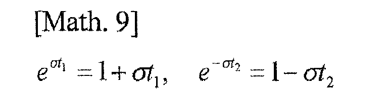
- Applying them into the above-mentioned expressions (9) and (10) yields the following expressions (13) and (14) during the respective periods when the
fourth switching element 14 is off and on.
[Math. 10]

That is, an output voltage having a triangular waveform is obtained. The bottom value v(0) and top value v(t2) of the output voltage having a triangular waveform are determined as in the following expressions.
[Math. 11]
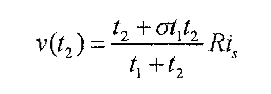
- When the capacity value C of the smoothing capacitor is further made greater, σ is approximated by 0, whereby the output voltage waveform asymptotically approaches a constant current value as in the following expression.

Here, coefficient p = t2/(t1+t2), which is the ratio of the on period to one cycle of on/off switching of thefourth switching element 14, is referred to as duty cycle of switching. Hence, a desirable output voltage is obtained when the duty cycle of thefourth switching element 14 is controlled. - Next, during a period when the
third switching element 13 is on, the first andfourth switching elements Figs. 3 and5 . Thesecond switching element 12 is subjected to PWM control at 120 kHz, for example. The output voltage waveform during the period when thethird switching element 13 is on has a polarity opposite to that of the above-mentioned period when thefirst switching element 11 is on. - When the first and
third switching elements Fig. 5 . Changing the above-mentioned duty cycle p with time in the PWM control of the second andfourth switching elements Fig. 5 . - Thus, by switching control of the second and
fourth switching elements third switching elements inverter 1 of the first embodiment can use switching elements which operate at relatively low speed and are less expensive as the first andthird switching elements third switching elements inverter 1 of the first embodiment can achieve lower cost. - Meanwhile, using a CMOSFET as a switching element in a bridge circuit is advantageous in that it is easily driven by a clock signal. However, a PMOSFET on the upper arm side is problematic in that it tends to exhibit an operating speed lower than that of an NMOSFET on the lower arm side, thereby making it hard to attain higher speed in switching control using a PWM scheme.
- Regarding this problem, the switching element on the upper arm side may also be constituted by an NMOSFET. This is advantageous in that higher speed in switching control by the NMOSFET is easier to achieve. However, this is problematic in that an insulating device such as a photocoupler is necessary in a drive circuit for the NMOSFET on the upper arm side, which impairs easiness in driving the switching element and makes it hard to achieve lower cost.
- In contrast, the
inverter 1 of the first embodiment is suitable when using a CMOSFET as a switching element and can achieve higher speed in switching control, easiness in driving the switching element, and lower cost. -
Fig. 6 is a circuit diagram illustrating the inverter in accordance with the second embodiment of the present invention. The inverter (power inverter circuit) 1A of the second embodiment is a three-phase bridge inverter. Theinverter 1A converts a DC power fed between a higher-voltage-side input terminal TIH and a lower-voltage-side input terminal TIL into a three-phase AC power among first to third output terminals TO1, TO2, TO3. Theinverter 1A differs from theinverter 1 of the first embodiment in that it further comprises fifth andsixth switching elements control circuit 20A in place of thecontrol circuit 20. - The fifth and
sixth switching elements fifth switching element 15 on the upper arm side is a PMOSFET, while thesixth switching element 16 on the lower arm side is an NMOSFET. - More specifically, the
fifth switching element 15 has a source terminal connected to the higher-voltage-side input terminals TIH and a drain terminal connected to a drain terminal of thesixth switching element 16. Thesixth switching element 16 has a source terminal connected to the lower-voltage-side input terminals TIL. The drain terminals of the fifth andsixth switching elements sixth switching elements control circuit 20A. - The
control circuit 20A performs switching control of the first tosixth switching elements 11 to 16. For example, thecontrol circuit 20A alternately turns on a set of the first andfourth switching elements sixth switching elements second switching elements - More specifically, in a 1/3-cycle period of the output three-phase AC power, the
control circuit 20A turns on thefirst switching element 11, while subjecting thefourth switching element 14 to switching control using a PWM scheme. In another 1/3-cycle period of the output three-phase AC power, thecontrol circuit 20A turns on thethird switching element 13, while subjecting thesixth switching element 16 to switching control using the PWM scheme. In still another 1/3-cycle period of the output three-phase AC power, thecontrol circuit 20A turns on thefifth switching element 15, while subjecting thesecond switching element 12 to switching control using the PWM scheme. - That is, the
control circuit 20A subjects the first, third, andfifth switching elements sixth switching elements fifth switching elements - By switching control of the second, fourth, and
sixth switching elements fifth switching elements inverter 1A of the second embodiment can also use switching elements which operate at relatively low speed and are less expensive as the first, third, andfifth switching elements fifth switching elements inverter 1A of the second embodiment can also achieve lower cost. - The present invention can be modified in various ways without being restricted to the above-mentioned embodiments. For example, while the embodiments illustrate a mode in which a CMOSFET is used as a switching element, i.e., a PMOSFET and an NMOSFET are used as switching elements on the upper and lower arm sides, respectively, the combination of switching elements on the upper and lower arm sides is not limited to that in the embodiments.
- For example, in any type of transistors such as those of IGBT (Insulated Gate Bipolar Transistor) and bipolar types, a switching element which has a conductivity type different from that of the switching element on the lower arm side and an operating speed lower than that of the switching element on the lower arm side may be used as a switching element on the upper arm side. Specifically, N- and P-channel transistors may be used as switching elements on the lower and upper arm sides, respectively.
- For example, a switching element which has a structure different from that of the switching element on the lower arm side and an operating speed lower than that of the switching element on the lower arm side may be used as a switching element on the upper arm side. Specifically, a switching element which can operate at relatively high speed may be selected from a group constituted by FETs, IGBTs, bipolar transistors, thyristors, and the like and used as a switching element on the lower arm side, while a switching element having relatively low operating speed and a structure different from that of the switching element on the lower arm side may be selected from a group constituted by FETs, IGBTs, bipolar transistors, thyristors, and the like and used as a switching element on the upper arm side.
- For example, a switching element which has a device different from that of the switching element on the lower arm side and an operating speed lower than that of the switching element on the lower arm side may be used as a switching element on the upper arm side. Specifically, a switching element constituted by an SiC device which can operate at relatively high speed may be used as a switching element on the lower arm side, while a switching element constituted by an SiC device having relatively low operating speed may be used as a switching element on the upper arm side.
- Though the switching elements on the lower arm side are subjected to switching control at a frequency higher than that of the switching elements on the upper arm side in the embodiments, the switching elements on the upper arm side may be subjected to switching control at a frequency higher than that of the switching elements on the lower arm side.
- The switching elements on the upper arm side (i.e., lower speed side), which are not subjected to switching control using the PWM scheme, may be subjected to switching control using the PWM scheme in a half-cycle period of the AC power when the switching elements on the upper arm side are on. Here, the switching frequency on the lower arm side is preferably at least twice as high as the switching frequency of the switching elements on the upper arm side. Preferably, in this case, the switching control on the lower arm side and that on the upper arm side are synchronized with each other.
- The present invention can be employed for lowering the cost of power inverter circuits.
-
- 1, 1A
- inverter (power inverter circuit)
- 11
- first switching element
- 12
- second switching element
- 13
- third switching element
- 14
- fourth switching element
- 15
- fifth switching element
- 16
- sixth switching element
- 20, 20A
- control circuit
- TIH
- higher-voltage-side input terminal
- TIL
- lower-voltage-side input terminal
- TO1
- first output terminal
- TO2
- second output terminal
- TO3
- third output terminal
Claims (6)
- A power inverter circuit comprising:first and second switching elements, sequentially connected in series between input terminals on higher and lower voltage sides, having an intermediate node connected to a first output terminal; andthird and fourth switching elements, sequentially connected in series between the input terminals on the higher and lower voltage sides, having an intermediate node connected to a second output terminal;the power inverter circuit alternatively turning on a set of the first and fourth switching elements and a set of the second and third switching elements so as to convert a DC power fed between the input terminals on the higher and lower voltage sides into an AC power between the first and second output terminals;wherein one of the sets of the first and third switching elements and the second and fourth switching elements is subjected to switching control at a frequency higher than that of the other.
- A power inverter circuit according to claim 1, wherein the set of the second and fourth switching elements is subjected to switching control at a frequency higher than that of the set of the first and third switching elements.
- A power inverter circuit according to claim 2, wherein the first switching element is turned on while the fourth switching element is subjected to switching control using a pulse width modulation scheme in a half-cycle period of the AC power when the first and fourth switching elements are on; and
wherein the third switching element is turned on while the second switching element is subjected to switching control using a pulse width modulation scheme in the other half-cycle period of the AC power when the second and third switching elements are on. - A power inverter circuit according to claim 2, wherein the first switching element is subjected to switching control using a pulse width modulation scheme while the fourth switching element is subjected to switching control using a pulse width modulation scheme at a frequency at least twice as high as the switching frequency of the first switching element in a half-cycle period of the AC power when the first and fourth switching elements are on; and
wherein the third switching element is subjected to switching control using a pulse width modulation scheme while the second switching element is subjected to switching control using a pulse width modulation scheme at a frequency at least twice as high as the switching frequency of the third switching element in the other half-cycle period of the AC power when the second and third switching elements are on. - A power inverter circuit according to claim 1, wherein the first to fourth switching elements are subjected to switching control so as to generate a single-phase AC power between the first and second output terminals.
- A power inverter circuit according to claim 1, further comprising fifth and sixth switching elements, sequentially connected in series between the input terminals on the higher and lower voltage sides, having an intermediate node connected to a third output terminal;
wherein the first to sixth switching elements are subjected to switching control such that one of sets of the first, third, and fifth switching elements and the second, fourth, and sixth switching elements is subjected to switching control at a frequency higher than that of the other so as to generate a three-phase AC power among the first to third output terminals.
Applications Claiming Priority (2)
| Application Number | Priority Date | Filing Date | Title |
|---|---|---|---|
| JP2012095308A JP2013223393A (en) | 2012-04-19 | 2012-04-19 | Power conversion circuit |
| PCT/JP2013/058342 WO2013157350A1 (en) | 2012-04-19 | 2013-03-22 | Power converter circuit |
Publications (2)
| Publication Number | Publication Date |
|---|---|
| EP2840698A1 true EP2840698A1 (en) | 2015-02-25 |
| EP2840698A4 EP2840698A4 (en) | 2017-04-12 |
Family
ID=49379981
Family Applications (1)
| Application Number | Title | Priority Date | Filing Date |
|---|---|---|---|
| EP13778128.2A Withdrawn EP2840698A4 (en) | 2012-04-19 | 2013-03-22 | Power converter circuit |
Country Status (6)
| Country | Link |
|---|---|
| US (1) | US9154052B2 (en) |
| EP (1) | EP2840698A4 (en) |
| JP (1) | JP2013223393A (en) |
| CN (1) | CN104205608B (en) |
| TW (1) | TWI571041B (en) |
| WO (1) | WO2013157350A1 (en) |
Families Citing this family (1)
| Publication number | Priority date | Publication date | Assignee | Title |
|---|---|---|---|---|
| TWI675539B (en) * | 2018-12-18 | 2019-10-21 | 沈志隆 | A power conversion device |
Family Cites Families (16)
| Publication number | Priority date | Publication date | Assignee | Title |
|---|---|---|---|---|
| JPS5341729A (en) * | 1976-09-29 | 1978-04-15 | Hitachi Ltd | Inverter |
| JPS56157275A (en) * | 1980-05-09 | 1981-12-04 | Toshiba Corp | Controlling device for inverter |
| JPS62177298U (en) * | 1986-04-24 | 1987-11-11 | ||
| JPS6499A (en) * | 1987-03-17 | 1989-01-05 | Nippon Kayaku Co Ltd | 23-phenylsteroids and production thereof |
| JPH03236004A (en) * | 1990-02-14 | 1991-10-22 | Mitsubishi Cable Ind Ltd | Self-supporting type optical fiber cable provided with slack portion |
| JPH0773404B2 (en) * | 1990-02-28 | 1995-08-02 | 澤藤電機株式会社 | Overcurrent protection device |
| JP3236318B2 (en) * | 1991-09-17 | 2001-12-10 | 松下冷機株式会社 | Operation control device for DC motor |
| JP2995373B2 (en) * | 1993-01-18 | 1999-12-27 | 株式会社三社電機製作所 | Control method of power supply for metal halide lamp |
| US6075717A (en) * | 1996-05-01 | 2000-06-13 | General Electric Company | PWM rectifier control with switching losses equally distributed among multiple switching devices |
| JP2000020006A (en) * | 1998-06-30 | 2000-01-21 | Denso Corp | Drive circuit for display device |
| JP2003088130A (en) * | 2001-09-07 | 2003-03-20 | Matsushita Electric Ind Co Ltd | Power converter with built-in battery |
| TWI327812B (en) * | 2006-11-28 | 2010-07-21 | Ind Tech Res Inst | Inverter circuit and control circuit thereof |
| JP2008236932A (en) * | 2007-03-22 | 2008-10-02 | Rohm Co Ltd | Motor drive device and electrical apparatus using this |
| JP2008278670A (en) * | 2007-05-01 | 2008-11-13 | Funai Electric Co Ltd | Separately-excited inverter circuit and liquid crystal television |
| CN101604923B (en) * | 2009-07-13 | 2012-05-16 | 西安理工大学 | Pulse width modulation (PWM) control method for single-phase grid-connected inverter |
| CN102035425B (en) * | 2010-12-28 | 2013-01-30 | 广东易事特电源股份有限公司 | Control method for inverter circuit of single-phase grid-connected inverter |
-
2012
- 2012-04-19 JP JP2012095308A patent/JP2013223393A/en active Pending
-
2013
- 2013-03-22 WO PCT/JP2013/058342 patent/WO2013157350A1/en not_active Ceased
- 2013-03-22 EP EP13778128.2A patent/EP2840698A4/en not_active Withdrawn
- 2013-03-22 CN CN201380018555.2A patent/CN104205608B/en not_active Expired - Fee Related
- 2013-03-28 US US13/852,805 patent/US9154052B2/en not_active Expired - Fee Related
- 2013-03-29 TW TW102111596A patent/TWI571041B/en not_active IP Right Cessation
Non-Patent Citations (1)
| Title |
|---|
| See references of WO2013157350A1 * |
Also Published As
| Publication number | Publication date |
|---|---|
| US20130279229A1 (en) | 2013-10-24 |
| CN104205608A (en) | 2014-12-10 |
| WO2013157350A1 (en) | 2013-10-24 |
| EP2840698A4 (en) | 2017-04-12 |
| CN104205608B (en) | 2017-05-17 |
| US9154052B2 (en) | 2015-10-06 |
| TWI571041B (en) | 2017-02-11 |
| JP2013223393A (en) | 2013-10-28 |
| TW201351867A (en) | 2013-12-16 |
Similar Documents
| Publication | Publication Date | Title |
|---|---|---|
| US8611120B2 (en) | Power conversion apparatus | |
| US8988915B2 (en) | DC to AC converter | |
| US9654036B2 (en) | Power conversion device and power conversion method | |
| EP2919377B1 (en) | Inverter device | |
| EP2975755A1 (en) | Solid-state power converters | |
| CN108471252A (en) | Inverter circuit, controller for motor and servo steering device | |
| JPH02501704A (en) | DC/DC power converter | |
| US9685885B2 (en) | Power conversion apparatus with an inverted-voltage generation circuit | |
| US9154052B2 (en) | Power inverter circuit having switching elements | |
| CN105391308A (en) | Matrix converter, matrix converter control device and matrix converter control method | |
| JP7166240B2 (en) | electronic circuit | |
| Bangarraju et al. | Power quality improvement using solar PV H-bridge based hybrid multilevel inverter | |
| JP6171701B2 (en) | Power converter | |
| Reznikov et al. | Re-visiting naturally balanced average capacitor voltages in multilevel DC-DC converters | |
| JP2007124731A (en) | Power converter | |
| EP1860761B1 (en) | Device and method for controlling inverters connected in series | |
| KR20160139955A (en) | Power conversion system for electric vehicles | |
| Bhambare et al. | Single phase to three phase MOSFET based inverter | |
| KR101522374B1 (en) | multi-Phases Sinusoidal PWM Inverter for High Efficiency | |
| Larbi et al. | Design and implementation of single phase solar inverter based on microcontroller 16F628A | |
| Dhekekar et al. | Study of performance analysis of H-bridge VSI with sinusoidal pulse width modulation | |
| KR20160116657A (en) | Control method for an ac motor using the reverse-phase control method, and the implemented system thereof | |
| Radetić et al. | RR complementary control method for transistor bridge converter | |
| JP2012191760A (en) | Power conversion device | |
| JPH02211067A (en) | Power supply equipment |
Legal Events
| Date | Code | Title | Description |
|---|---|---|---|
| PUAI | Public reference made under article 153(3) epc to a published international application that has entered the european phase |
Free format text: ORIGINAL CODE: 0009012 |
|
| 17P | Request for examination filed |
Effective date: 20140930 |
|
| AK | Designated contracting states |
Kind code of ref document: A1 Designated state(s): AL AT BE BG CH CY CZ DE DK EE ES FI FR GB GR HR HU IE IS IT LI LT LU LV MC MK MT NL NO PL PT RO RS SE SI SK SM TR |
|
| AX | Request for extension of the european patent |
Extension state: BA ME |
|
| DAX | Request for extension of the european patent (deleted) | ||
| RA4 | Supplementary search report drawn up and despatched (corrected) |
Effective date: 20170313 |
|
| RIC1 | Information provided on ipc code assigned before grant |
Ipc: H02M 7/48 20070101ALI20170307BHEP Ipc: H02M 7/5387 20070101AFI20170307BHEP Ipc: H02M 7/538 20070101ALI20170307BHEP |
|
| STAA | Information on the status of an ep patent application or granted ep patent |
Free format text: STATUS: REQUEST FOR EXAMINATION WAS MADE |
|
| STAA | Information on the status of an ep patent application or granted ep patent |
Free format text: STATUS: THE APPLICATION IS DEEMED TO BE WITHDRAWN |
|
| 18D | Application deemed to be withdrawn |
Effective date: 20171010 |