EP2837026B1 - Cte matched interposer and method of making - Google Patents
Cte matched interposer and method of making Download PDFInfo
- Publication number
- EP2837026B1 EP2837026B1 EP13775666.4A EP13775666A EP2837026B1 EP 2837026 B1 EP2837026 B1 EP 2837026B1 EP 13775666 A EP13775666 A EP 13775666A EP 2837026 B1 EP2837026 B1 EP 2837026B1
- Authority
- EP
- European Patent Office
- Prior art keywords
- interposer
- substrate
- metal
- filled
- collar
- Prior art date
- Legal status (The legal status is an assumption and is not a legal conclusion. Google has not performed a legal analysis and makes no representation as to the accuracy of the status listed.)
- Active
Links
Images


Classifications
-
- H—ELECTRICITY
- H01—ELECTRIC ELEMENTS
- H01L—SEMICONDUCTOR DEVICES NOT COVERED BY CLASS H10
- H01L23/00—Details of semiconductor or other solid state devices
- H01L23/12—Mountings, e.g. non-detachable insulating substrates
- H01L23/14—Mountings, e.g. non-detachable insulating substrates characterised by the material or its electrical properties
- H01L23/147—Semiconductor insulating substrates
-
- H—ELECTRICITY
- H01—ELECTRIC ELEMENTS
- H01L—SEMICONDUCTOR DEVICES NOT COVERED BY CLASS H10
- H01L23/00—Details of semiconductor or other solid state devices
- H01L23/48—Arrangements for conducting electric current to or from the solid state body in operation, e.g. leads, terminal arrangements ; Selection of materials therefor
- H01L23/488—Arrangements for conducting electric current to or from the solid state body in operation, e.g. leads, terminal arrangements ; Selection of materials therefor consisting of soldered or bonded constructions
- H01L23/498—Leads, i.e. metallisations or lead-frames on insulating substrates, e.g. chip carriers
- H01L23/49838—Geometry or layout
-
- H—ELECTRICITY
- H01—ELECTRIC ELEMENTS
- H01L—SEMICONDUCTOR DEVICES NOT COVERED BY CLASS H10
- H01L23/00—Details of semiconductor or other solid state devices
- H01L23/32—Holders for supporting the complete device in operation, i.e. detachable fixtures
-
- H—ELECTRICITY
- H01—ELECTRIC ELEMENTS
- H01L—SEMICONDUCTOR DEVICES NOT COVERED BY CLASS H10
- H01L21/00—Processes or apparatus adapted for the manufacture or treatment of semiconductor or solid state devices or of parts thereof
- H01L21/02—Manufacture or treatment of semiconductor devices or of parts thereof
- H01L21/04—Manufacture or treatment of semiconductor devices or of parts thereof the devices having at least one potential-jump barrier or surface barrier, e.g. PN junction, depletion layer or carrier concentration layer
- H01L21/48—Manufacture or treatment of parts, e.g. containers, prior to assembly of the devices, using processes not provided for in a single one of the subgroups H01L21/06 - H01L21/326
- H01L21/4814—Conductive parts
- H01L21/4846—Leads on or in insulating or insulated substrates, e.g. metallisation
- H01L21/486—Via connections through the substrate with or without pins
-
- H—ELECTRICITY
- H01—ELECTRIC ELEMENTS
- H01L—SEMICONDUCTOR DEVICES NOT COVERED BY CLASS H10
- H01L23/00—Details of semiconductor or other solid state devices
- H01L23/28—Encapsulations, e.g. encapsulating layers, coatings, e.g. for protection
- H01L23/31—Encapsulations, e.g. encapsulating layers, coatings, e.g. for protection characterised by the arrangement or shape
- H01L23/3107—Encapsulations, e.g. encapsulating layers, coatings, e.g. for protection characterised by the arrangement or shape the device being completely enclosed
- H01L23/3142—Sealing arrangements between parts, e.g. adhesion promotors
-
- H—ELECTRICITY
- H01—ELECTRIC ELEMENTS
- H01L—SEMICONDUCTOR DEVICES NOT COVERED BY CLASS H10
- H01L23/00—Details of semiconductor or other solid state devices
- H01L23/48—Arrangements for conducting electric current to or from the solid state body in operation, e.g. leads, terminal arrangements ; Selection of materials therefor
- H01L23/488—Arrangements for conducting electric current to or from the solid state body in operation, e.g. leads, terminal arrangements ; Selection of materials therefor consisting of soldered or bonded constructions
- H01L23/498—Leads, i.e. metallisations or lead-frames on insulating substrates, e.g. chip carriers
- H01L23/49811—Additional leads joined to the metallisation on the insulating substrate, e.g. pins, bumps, wires, flat leads
- H01L23/49816—Spherical bumps on the substrate for external connection, e.g. ball grid arrays [BGA]
-
- H—ELECTRICITY
- H01—ELECTRIC ELEMENTS
- H01L—SEMICONDUCTOR DEVICES NOT COVERED BY CLASS H10
- H01L23/00—Details of semiconductor or other solid state devices
- H01L23/48—Arrangements for conducting electric current to or from the solid state body in operation, e.g. leads, terminal arrangements ; Selection of materials therefor
- H01L23/488—Arrangements for conducting electric current to or from the solid state body in operation, e.g. leads, terminal arrangements ; Selection of materials therefor consisting of soldered or bonded constructions
- H01L23/498—Leads, i.e. metallisations or lead-frames on insulating substrates, e.g. chip carriers
- H01L23/49827—Via connections through the substrates, e.g. pins going through the substrate, coaxial cables
-
- H—ELECTRICITY
- H01—ELECTRIC ELEMENTS
- H01L—SEMICONDUCTOR DEVICES NOT COVERED BY CLASS H10
- H01L23/00—Details of semiconductor or other solid state devices
- H01L23/48—Arrangements for conducting electric current to or from the solid state body in operation, e.g. leads, terminal arrangements ; Selection of materials therefor
- H01L23/488—Arrangements for conducting electric current to or from the solid state body in operation, e.g. leads, terminal arrangements ; Selection of materials therefor consisting of soldered or bonded constructions
- H01L23/498—Leads, i.e. metallisations or lead-frames on insulating substrates, e.g. chip carriers
- H01L23/49833—Leads, i.e. metallisations or lead-frames on insulating substrates, e.g. chip carriers the chip support structure consisting of a plurality of insulating substrates
-
- H—ELECTRICITY
- H01—ELECTRIC ELEMENTS
- H01L—SEMICONDUCTOR DEVICES NOT COVERED BY CLASS H10
- H01L23/00—Details of semiconductor or other solid state devices
- H01L23/52—Arrangements for conducting electric current within the device in operation from one component to another, i.e. interconnections, e.g. wires, lead frames
- H01L23/538—Arrangements for conducting electric current within the device in operation from one component to another, i.e. interconnections, e.g. wires, lead frames the interconnection structure between a plurality of semiconductor chips being formed on, or in, insulating substrates
- H01L23/5384—Conductive vias through the substrate with or without pins, e.g. buried coaxial conductors
-
- H—ELECTRICITY
- H01—ELECTRIC ELEMENTS
- H01L—SEMICONDUCTOR DEVICES NOT COVERED BY CLASS H10
- H01L2224/00—Indexing scheme for arrangements for connecting or disconnecting semiconductor or solid-state bodies and methods related thereto as covered by H01L24/00
- H01L2224/01—Means for bonding being attached to, or being formed on, the surface to be connected, e.g. chip-to-package, die-attach, "first-level" interconnects; Manufacturing methods related thereto
- H01L2224/10—Bump connectors; Manufacturing methods related thereto
- H01L2224/15—Structure, shape, material or disposition of the bump connectors after the connecting process
- H01L2224/16—Structure, shape, material or disposition of the bump connectors after the connecting process of an individual bump connector
-
- H—ELECTRICITY
- H01—ELECTRIC ELEMENTS
- H01L—SEMICONDUCTOR DEVICES NOT COVERED BY CLASS H10
- H01L2924/00—Indexing scheme for arrangements or methods for connecting or disconnecting semiconductor or solid-state bodies as covered by H01L24/00
- H01L2924/10—Details of semiconductor or other solid state devices to be connected
- H01L2924/146—Mixed devices
- H01L2924/1461—MEMS
Definitions
- the present invention relates to semiconductor packaging In particular it relates to an interposer with matched coefficient of thermal expansion (CTE).
- CTE coefficient of thermal expansion
- interposers it is desirable to be able to stack chips carrying various devices on top of each other. Also, it is desirable to be able to provide so called redistribution layers or routing structures for signals coming from integrated circuits having large numbers of I/O contacts. Such contacts can be as many as several thousand on a chip of a size of the order of 10 mm square. If the signals are to be routed through the substrate, the through-substrate connections (vias) would have to be equally closely spaced. When such vias are made of metal and very closely spaced, thermal expansion effects due to different coefficients of expansion may cause damage to the very thin and brittle chips in which they are made. This frequently occurs both during processing but also in use in the end product, if it is subjected to temperature changes over large intervals. Also, the thickness of the substrate for such vias would have to be in the order of 100 ⁇ m, which is extremely.
- routings are "fanned out", i.e. the individual conductive strips diverge from the I/O points to a more widely spaced structure, where vias for routing through the substrate are provided.
- the thickness of the substrate normally cannot be as small as 100 ⁇ m without the use of carriers, but rather 300 ⁇ m and more is more reasonable not requiring carriers.
- 300 ⁇ m thick wafers it is difficult not to say impossible to make void free hermetically tight vias of the size desirable, e.g. 15-100 ⁇ m in diameter, that extend through the substrate, in a cost efficient manner, i.e. in volume production.
- Fig. 1 there is shown a prior art structure disclosed in applicants own WO 2007/089206 A1 .
- routing from a via to a contact pad on a remote location on the substrate is provided by a two-step etching process, wherein via holes are first made, and then recesses are made in a subsequent step.
- These routing structures will be in-plane and the vias are filled. Thermal expansion issues may occur if high density TSVs are to be used.
- FIG. 2 another prior art via structure is shown, details of which are disclosed in applicants own WO 2010/059118 .
- This via structure comprises a wide and deep part extending form one side of the wafer, and a shallow and narrow part extending from the other side.
- a liner via When the via is metallized, only the walls of the wide part is covered (referred to as a "liner via") whereas the narrow part is completely filled.
- This structure is advantageous in that thermal effects due to different expansion properties of metal and silicon will not have a major influence despite close-packing of the vias. It also requires less process time with regards to Electrochemical deposition (ECD) of metal (e.g. Cu).
- ECD Electrochemical deposition
- EP-2 165 362 ( ⁇ AC Microtec AB) a process referred to as the XiViaTM process is disclosed.
- KOH etching is used and when it is scaled to higher densities (i.e. smaller holes with larger aspect ratios), the KOH yields a sloping surface that will occupy to much area to make higher densities possible.
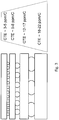
- Fig. 3 is a schematic cross-section showing different values of CTE in a stack of components (a so called "CTE pyramid for interposers")
- Fig. 4 schematically shows an example of a prior art solution to the problem of temperature matching of components with large differences in CTE.
- IC integrated circuits
- I/O interposer
- CTE a CTE of about 3 ppm/C.
- I/O interposer
- a CTE of about 3 ppm/C silicon or glass interposer IP
- a Module/Processor PCB having a high CTE of about 18-22 ppm/C.
- BGA All Grid Array
- underfill between on one hand the IC component and the interposer, and on the other between the PCB and the BGA substrate.
- This underfill is applied as a liquid that is drawn into the very small spacing by capillary force.
- An interposer according to the invention is defined in claim 1.
- the benefit of using a rigid interposer is i.a. an ability to create TSVs through full wafer thickness.
- the stress gradient across a thick interposer is reduced, and it can be directly attached to the PCB and will accommodate stresses.
- rigid interposers best take advantage of existing wafer processing, and there is no need for complex thin wafer handling.
- the inventive merit of the present interposer is that it is possible to taylor the coefficient of thermal expansion CTE of the interposer to match components to be attached thereto within very wide ranges.
- the invention eliminates organic substrates which improves heat transfer, thermal matching of die to package.
- a silicon substrate can furthermore be “functionalized” by incorporating passive (resistances, capacitances, inductances) or active elements (e.g. diodes and ESD protection), which is not possible with organic substrates.
- a further advantage is a more cost efficient structure, in that only one substrate is needed.
- a method of making an interposer comprising providing a substrate having a front side and a back side; making a double via having a narrow part and a wide part; depositing metal at least as a liner layer inside the via on its walls; providing redistribution structures in the surface(s) of the substrate which are flush with at least the front side of the substrate; making contact elements on the redistribution structures on the front side, said contact elements having an aspect ratio, height:diameter ⁇ 1:1, preferably 1:1 to 2:1.
- wafers are disclosed with hermetically sealed and close-packed vias and with in-plane routing patterns, such that the advantages of both of the above described prior art structures are combined in one structure.
- the prior art structure according to Fig. 1 comprises a conventional metal via, where the diameter is in the order of 300 ⁇ m.
- This structure is fairly easy to manufacture as long as the pitch, i.e. center-to-center distance between vias is not too small. Density of vias is of course also important.
- thermal stress effects may easily cause damage to the substrate, both during manufacture and use.
- the diameter of the via holes must be reduced.
- the aspect ratio (Depth/Width) is high, i.e. is more than 2:1, and even for aspect ratios down to 1:1 it may be difficult, due to the nature of the PVD process and step coverage.
- the seed layer on the field i.e. the flat wafer area surrounding the vias and the RDL structures
- the seed layer on the field i.e. the flat wafer area surrounding the vias and the RDL structures
- the RDL are to be made needs to be thick and therefore makes densely packed redistribution wires with small feature size difficult to obtain, when the seed layer is to be removed by wet etching processes.
- Fig. 2 is very flexible/adaptable in terms of the amount of metal that can be introduced in it.
- the top portion is filled with metal, whereas the bottom portion has only the walls thereof coated, as a "liner" of metal.
- this liner thicker or thinner, the temperature expansion properties can be varied to adapt to components to be attached to the interposer, primarily by virtue of there being air present in the via, which renders it able to accommodate movements. Instead letting air being present other materials can be provided, which is described further below.
- Interposers in general are used for connecting devices having high density I/Os with devices having low density I/Os.
- matching of devices having different CTE is made by using a so called underfill, which is a material that is applied in the very small spacing between a device having one CTE and another device having a differing CTE.
- the inventive merit of the present interposer is that it is possible to taylor the coefficient of thermal expansion CTE of the interposer to match components to be attached thereto within very wide ranges.
- the invention essentially resides in the adaption of the CTE of the interposer to the extremes in CTE represented by the silicon die on one side of the interposer and the plastic or ceramic circuit board on the other side of the interposer.
- the CTE of the interposer is thereby selected to be somewhere in between these extremes, which prevents undue strain and stress that the interposer otherwise might be subjected to.
- One way is to select the width of the via holes according to the situation, where wider vias (i.e. more metal) will increase the CTE and narrower vias will reduce the CTE.
- wider vias i.e. more metal
- narrower vias will reduce the CTE.
- the routing structures can also be made to exhibit primarily larger depth. The width would normally be required to be small because of the need to close-pack the structures.
- Another method is to provide thermal expansion matching structures, i.e. non-functional vias and/or recesses. Thereby the width and depth of the recesses and vias can be taylored to the situation at hand, and also the density of structures can be increased if required.
- Fig. 5 schematically illustrates the invention showing a plurality of integrated circuits IC on top of the interposer which is attached directly to a circuit board PCB.
- the interposer is one single, rigid component structure IP that replaces the multi-layered structure according to prior art ( Fig. 4 ).
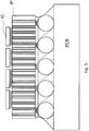
- Fig. 6 illustrates an embodiment of an interposer in more detail. It comprises a substrate 10 in which double vias 18, 28 have been made.
- the double vias comprise a wide 28 and a narrow portion 18, and in the shown embodiment the narrow part is filled with metal 27 whereas the wider portion only has a "liner layer" of metal provided.
- routing 20 on the front side FS on which contact elements, suitably pillars ⁇ SB, are provided. These contact elements help in accommodating lateral movements due to thermal effects.
- On the back side BS there are further routing and contacts, e.g. Ball Grid Arrays BGA.
- the contact elements (pillars) are made of copper or at least are copper based.
- Fig. 7 illustrates an embodiment of an interposer according to the invention having the mentioned "double" vias and connecting a printed circuit board PCB with a silicon device SD on top, said device having a high density of I/O:s, i.e. very close spacing between them.
- the circuit board which can be a laminate, PCB, Ceramic etc with a low density of I/O:s, is attached.
- contact elements in the form of contact elements ⁇ SB with a very small pitch (e.g. 50 ⁇ m spacing), or regular SMD solder ⁇ -bumps.
- the contact elements will exhibit dimensions of 20-50 ⁇ m in diameter and a height of 30-100 ⁇ m. A preferred diameter would be about 40 ⁇ m and a preferred height about 60 ⁇ m, giving an aspect ratio of 1,5:1.
- underfill UF is also provided in conventional manner between the interposer and the silicon device on the top. In particular the underfill makes it possible to fine-tune the CTE matching by providing more or less underfill between the upper components.
- the copper contact elements are made by Cu plating or other techniques well known to the skilled man in semiconductor packaging art.
- thermal expansion matching structures the sole purpose of which are to provide an adapted CTE value for the interposer.
- thermal expansion matching structures Examples of such thermal expansion matching structures are shown in Fig. 8 .
- the thermal expansion matching structure is provided as a double via DDV as shown previously, but where there are no connections to components, i.e. the via has an identical constitution as the "active" double vias but is not connected to any active components, and is thus only used for the purpose of introducing more metal in the interposer.
- the thermal expansion matching structure has a relatively thin liner layer LL of metal.
- a second example is where there is only provided a thermal expansion matching structure in the form of a recess DR in the front side (top surface as seen in the figure) and filling it with metal.
- thermal expansion matching structures can be varied within wide ranges.
- This hole is a wider hole having only a liner LL on the inner walls.
- the liner layer is shown, as an example, with at thicker liner layer LL.
- the above process is usable for relatively thick substrates, i.e. exhibiting a thickness in the order of 300 ⁇ m and more, which is a rigid enough wafer to be compatible with automatic semiconductor handling without the need for stabilizing carrier solution.
- Fig. 9 illustrates a further embodiment where the interposer IP has been provided with RDL structures 20 in several layers, suitably made by a damascene process.
- the material in which the actual routings (which are metal) are made is normally an insulator such as an oxide.
- this material in itself will exhibit a different CTE compared to the silicon in the interposer, and thus also this layered structure can also be made to provide some CTE matching.
- a further possibility to "fine tune" the CTE adjustment is illustrated in Fig. 10 .
- the remaining voids can be filled with a further elastic material P having a different CTE than the metal.
- a further elastic material P having a different CTE than the metal.
- Such material can be e.g. an elastic polymer such as a siloxane based photosensitive permanent resist, obtainable e.g. from Shinetsu under the treadname SINR®, or off stoichmetric thiol-enes (OSTE), or low temperature poly-silicon.
- Poly-silicon is of course not elastic but has a suitable CTE value that yields a similar effect as the elastic polymers.
- Fig. 10a there is shown an example not falling under the claimed invention of a "double via", having a wide part and a narrow part, where there is a liner layer LLM only of metal covering the inner walls of the via, and the elastic further material P is provided so as to fill up the void.
- Fig. 10b an example according to the invention is shown.
- the upper part of the structure i.e. the narrow part of the via and, optionally if present, also the routing structure
- metal M is completely filled with metal M
- the lower, wider part only has a liner layer, and the void in the wider part is filled with the elastic further material P.
- This feature is of course applicable in all combinations of structures as described herein, although not explicitly shown.
- One further advantage of providing a further material P as shown is that contact pads can be provided on the exposed surfaces of this material, which further improves the temperature matching.
- solder balls BGA should be slightly displaced from center such they cover the material in the liner layer only to one side, see Fig. 10a arrow at D. In this way any movement due to thermal stress will be accommodated by the combination of the solder ball and the elastic further material P provided in the via.
- Figs. 10c and 10d do not fall under the claimed invention.
- a collar C around the via is provided.
- the collar C is flush with the surrounding substrate 10 surface, and the solder ball BGA is attached partly to this collar C and partly supported by the further material P in the via. Thereby a better electrical contact is ascertained.
- a collar C' is provided. However, in this case the collar is raised above the surrounding substrate surface.
- solder balls BGA are provided entirely on the substrate.
- nay movements are entirely accommodated by the solder ball, which may cause it to shear to the extent that it breaks.
Description
- The present invention relates to semiconductor packaging In particular it relates to an interposer with matched coefficient of thermal expansion (CTE).
- In modern electronic devices such as mobile phones, computers etc. there is a continuous strive for miniaturization and close-packing of components. In the continuous strive of making micro components more densely packed, problems are encountered in particular where wafer through structures (also referred to as vias) are provided in very close proximity to each other. In particular where the vias are made from a material that is different from the substrate material in which they are provided, e.g. metal and silicon in the vias and substrate respectively, different thermal expansion effects may lead to substrates being subject to cracking and breaking during manufacturing, or other reliability issues during use.
- Among other things it is desirable to be able to stack chips carrying various devices on top of each other, so called interposers. Also, it is desirable to be able to provide so called redistribution layers or routing structures for signals coming from integrated circuits having large numbers of I/O contacts. Such contacts can be as many as several thousand on a chip of a size of the order of 10 mm square. If the signals are to be routed through the substrate, the through-substrate connections (vias) would have to be equally closely spaced. When such vias are made of metal and very closely spaced, thermal expansion effects due to different coefficients of expansion may cause damage to the very thin and brittle chips in which they are made. This frequently occurs both during processing but also in use in the end product, if it is subjected to temperature changes over large intervals. Also, the thickness of the substrate for such vias would have to be in the order of 100 µm, which is extremely.
- Thus, in modern electronic devices such as mobile phones, the different thermal expansion coefficients for the various materials in the housing, the circuit boards, and the micro chips (MEMS, CMOS and the like), respectively, inevitably will cause problems unless relevant design measures are taken.
- It is not suitable to provide routing by vias directly from each I/O point on a IC chip through the substrate on which the chip is mounted. Instead one provides for the above mentioned redistribution structures on the surface of the substrate on which the chip is mounted. The routings are "fanned out", i.e. the individual conductive strips diverge from the I/O points to a more widely spaced structure, where vias for routing through the substrate are provided.
- However, even with such precautions there will be a tendency for thermal stress in the interface between the I/O points and the substrate. To alleviate this effect a conventional procedure is to provide so called "underfill" in the very small space between the substrate and IC chip, using capillary forces. However, this requires that the vias are completely filled to be hermetically sealed such that there will be no leakage of underfill between the stacked structures, which could lead to improper underfill, degradation of the final product, reliability issues and packing issues, rendering final product useless.
- Thus, it is desirable to provide filled vias. However, filling conventional vias with metal again will bring the thermal expansion effects into play, in particular if they were to be provided directly beneath the IC chip.
- Also, as mentioned above, from a processing point of view, the thickness of the substrate normally cannot be as small as 100 µm without the use of carriers, but rather 300 µm and more is more reasonable not requiring carriers. However, for 300 µm thick wafers it is difficult not to say impossible to make void free hermetically tight vias of the size desirable, e.g. 15-100 µm in diameter, that extend through the substrate, in a cost efficient manner, i.e. in volume production.
- No suitable conductive metal for making TSVs that has CTE that matches the Silicon is known at present.
- In
Fig. 1 there is shown a prior art structure disclosed in applicants ownWO 2007/089206 A1 . Here, routing from a via to a contact pad on a remote location on the substrate is provided by a two-step etching process, wherein via holes are first made, and then recesses are made in a subsequent step. These routing structures will be in-plane and the vias are filled. Thermal expansion issues may occur if high density TSVs are to be used. - In
Fig. 2 another prior art via structure is shown, details of which are disclosed in applicants ownWO 2010/059118 . This via structure comprises a wide and deep part extending form one side of the wafer, and a shallow and narrow part extending from the other side. When the via is metallized, only the walls of the wide part is covered (referred to as a "liner via") whereas the narrow part is completely filled. This structure is advantageous in that thermal effects due to different expansion properties of metal and silicon will not have a major influence despite close-packing of the vias. It also requires less process time with regards to Electrochemical deposition (ECD) of metal (e.g. Cu). - When routing layers are provided on a structure as the one above, a disadvantage is that it results in topography.
- In
EP-2 165 362 (ÅAC Microtec AB) a process referred to as the XiVia™ process is disclosed. In this process KOH etching is used and when it is scaled to higher densities (i.e. smaller holes with larger aspect ratios), the KOH yields a sloping surface that will occupy to much area to make higher densities possible. - When integrated circuits are to be mounted on traditional circuit boards, the differences in thermal expansion due to environmental influence and other factors come into play. In fact, devices can be broken during use due to forces occurring during thermal expansion.
- Further teaching related to the present disclosure can be found in
KR 2009 0120167 A WO 2013/137809 A1 . -
Fig. 3 is a schematic cross-section showing different values of CTE in a stack of components (a so called "CTE pyramid for interposers"), andFig. 4 schematically shows an example of a prior art solution to the problem of temperature matching of components with large differences in CTE. - Thus, on top of the stacked structure shown in
Fig. 3-4 there is one or more integrated circuits IC, e.g. ASICs or other components, with high density I/O:s and a CTE of about 3 ppm/C. These components are attached to a silicon or glass interposer IP which a CTE of 5-8 ppm/C. At the bottom of the stack there is a Module/Processor PCB having a high CTE of about 18-22 ppm/C. In order to match the CTEs one has to provide a BGA (Ball Grid Array) substrate having a CTE of about 12-17 PPM/C between the PCB and the glass/silicon interposer. - Furthermore, in order to provide enhanced CTE matching there is provided so called underfill between on one hand the IC component and the interposer, and on the other between the PCB and the BGA substrate.
- This underfill is applied as a liquid that is drawn into the very small spacing by capillary force.
- This structure is fairly complicated to handle since the interposer and the BGA substrate are very thin. Thus, it would be desirable to have an interposer structure that both provides the required CTE matching and ease of handling.
- In view of the demands mentioned above and the shortcomings of the state of the art technology, the inventors have devised a new interposer which overcome the problem of the prior art relating to the complexity of the structures required for CTE matching.
- An interposer according to the invention is defined in claim 1.
- The benefit of using a rigid interposer is i.a. an ability to create TSVs through full wafer thickness. The stress gradient across a thick interposer is reduced, and it can be directly attached to the PCB and will accommodate stresses.
- Also, rigid interposers best take advantage of existing wafer processing, and there is no need for complex thin wafer handling.
- The inventive merit of the present interposer is that it is possible to taylor the coefficient of thermal expansion CTE of the interposer to match components to be attached thereto within very wide ranges.
- The invention eliminates organic substrates which improves heat transfer, thermal matching of die to package. A silicon substrate can furthermore be "functionalized" by incorporating passive (resistances, capacitances, inductances) or active elements (e.g. diodes and ESD protection), which is not possible with organic substrates.
- A further advantage is a more cost efficient structure, in that only one substrate is needed.
- In another aspect there is provided a method of making an interposer, defined in
claim 10. The method comprises providing a substrate having a front side and a back side; making a double via having a narrow part and a wide part; depositing metal at least as a liner layer inside the via on its walls; providing redistribution structures in the surface(s) of the substrate which are flush with at least the front side of the substrate; making contact elements on the redistribution structures on the front side, said contact elements having an aspect ratio, height:diameter < 1:1, preferably 1:1 to 2:1. - Further scope of applicability of the present invention will become apparent from the detailed description given hereinafter and the accompanying drawings which are given by way of illustration only, and thus not to be considered limiting on the present invention, and wherein
-
Fig. 1 shows a prior art structure with a filled via wherein the routing from a via is in-plane; -
Fig. 2 illustrates a prior art via comprising a wide part and a narrow part wherein only the narrow part is filled with metal. -
Fig. 3 is an illustration of a so called reliability pyramid, showing temperature matching requirements; -
Fig. 4 is a schematic illustration of a prior art CTE matched interposer structure; -
Fig. 5 shows schematically a structure according to the invention, i.e. one single rigid interposer that replaces the two components of the prior art, i.e. the glass/silicon interposer and the ball grid array. -
Fig. 6 illustrates the invention in more detail; -
Fig. 7 illustrates an interposer mounted between a PCB and silicon device; -
Fig. 8 illustrates an interposer in use having dedicated structures for CTE compensation; -
Fig. 9 illustrates an interposer provided with multiple Redistribution Layers (RDL); and -
Fig. 10a-d shows further embodiments for providing CTE matching. - Herein wafers are disclosed with hermetically sealed and close-packed vias and with in-plane routing patterns, such that the advantages of both of the above described prior art structures are combined in one structure.
- The prior art structure according to
Fig. 1 comprises a conventional metal via, where the diameter is in the order of 300 µm. This structure is fairly easy to manufacture as long as the pitch, i.e. center-to-center distance between vias is not too small. Density of vias is of course also important. For a "fully propagated" wafer wherein the pitch is in the range of twice the diameter of the vias thermal stress effects may easily cause damage to the substrate, both during manufacture and use. - Consequently, if it is desired to provide more closely packed via structures the diameter of the via holes must be reduced. However, for small diameters it becomes very difficult with common prior art technologies like PVD to provide the seed layer in the holes for subsequent plating, and in particular to provide a conformal seed layer,_ if the aspect ratio (Depth/Width) is high, i.e. is more than 2:1, and even for aspect ratios down to 1:1 it may be difficult, due to the nature of the PVD process and step coverage. The seed layer on the field (i.e. the flat wafer area surrounding the vias and the RDL structures) where the RDL are to be made needs to be thick and therefore makes densely packed redistribution wires with small feature size difficult to obtain, when the seed layer is to be removed by wet etching processes.
- This problem is solved by using methods disclosed in co-pending international applications
PCT/SE2013/050225 PCT/SE2013/050353
The structure according toFig. 2 is very flexible/adaptable in terms of the amount of metal that can be introduced in it. In the embodiment shown in the figures, especially the final structure inFig. 6 , it is seen that the top portion is filled with metal, whereas the bottom portion has only the walls thereof coated, as a "liner" of metal. By making this liner thicker or thinner, the temperature expansion properties can be varied to adapt to components to be attached to the interposer, primarily by virtue of there being air present in the via, which renders it able to accommodate movements. Instead letting air being present other materials can be provided, which is described further below. - Interposers in general are used for connecting devices having high density I/Os with devices having low density I/Os. Normally, matching of devices having different CTE is made by using a so called underfill, which is a material that is applied in the very small spacing between a device having one CTE and another device having a differing CTE.
- The inventive merit of the present interposer is that it is possible to taylor the coefficient of thermal expansion CTE of the interposer to match components to be attached thereto within very wide ranges.
- The invention essentially resides in the adaption of the CTE of the interposer to the extremes in CTE represented by the silicon die on one side of the interposer and the plastic or ceramic circuit board on the other side of the interposer. The CTE of the interposer is thereby selected to be somewhere in between these extremes, which prevents undue strain and stress that the interposer otherwise might be subjected to.
- There are several ways to achieve this result.
- One way is to select the width of the via holes according to the situation, where wider vias (i.e. more metal) will increase the CTE and narrower vias will reduce the CTE. Of course the routing structures can also be made to exhibit primarily larger depth. The width would normally be required to be small because of the need to close-pack the structures.
- Another method is to provide thermal expansion matching structures, i.e. non-functional vias and/or recesses. Thereby the width and depth of the recesses and vias can be taylored to the situation at hand, and also the density of structures can be increased if required.
-
Fig. 5 schematically illustrates the invention showing a plurality of integrated circuits IC on top of the interposer which is attached directly to a circuit board PCB. The interposer is one single, rigid component structure IP that replaces the multi-layered structure according to prior art (Fig. 4 ). -
Fig. 6 illustrates an embodiment of an interposer in more detail. It comprises asubstrate 10 in whichdouble vias narrow portion 18, and in the shown embodiment the narrow part is filled withmetal 27 whereas the wider portion only has a "liner layer" of metal provided. There also is providedrouting 20 on the front side FS, on which contact elements, suitably pillars µSB, are provided. These contact elements help in accommodating lateral movements due to thermal effects. On the back side BS there are further routing and contacts, e.g. Ball Grid Arrays BGA. Preferably the contact elements (pillars) are made of copper or at least are copper based. -
Fig. 7 illustrates an embodiment of an interposer according to the invention having the mentioned "double" vias and connecting a printed circuit board PCB with a silicon device SD on top, said device having a high density of I/O:s, i.e. very close spacing between them. On the bottom side the circuit board which can be a laminate, PCB, Ceramic etc with a low density of I/O:s, is attached. - These attached components have different CTE values and if attached directly to each other thermal effects would cause strains that might tear the components apart and render them non-functional. By virtue of the design of the via it is possible to adapt the metal amount so as to create a CTE value for the interposer as a whole that matches the differences in CTE of the components and thereby essentially eliminates the risk of thermal stress fractures.
- As mentioned, on the top side of the interposer there can be provided contact elements in the form of contact elements µSB with a very small pitch (e.g. 50 µm spacing), or regular SMD solder µ-bumps.
- The contact elements connect to the I/Os of the device on top, and by virtue of their small size and their aspect ratio (height/diameter = 1:1 to 2:1) they will be able to accommodate any lateral movements caused by thermal influences, i.e. they will absorb any shear forces that may occur. The contact elements will exhibit dimensions of 20-50 µm in diameter and a height of 30-100 µm. A preferred diameter would be about 40 µm and a preferred height about 60 µm, giving an aspect ratio of 1,5:1. In order to further enhance the behaviour underfill UF is also provided in conventional manner between the interposer and the silicon device on the top. In particular the underfill makes it possible to fine-tune the CTE matching by providing more or less underfill between the upper components.
- The copper contact elements are made by Cu plating or other techniques well known to the skilled man in semiconductor packaging art.
- However, it is also possible to use the methods disclosed in the mentioned co-pending applications to create thermal expansion matching structures, the sole purpose of which are to provide an adapted CTE value for the interposer.
- Examples of such thermal expansion matching structures are shown in
Fig. 8 . - Thus, a first example is where the thermal expansion matching structure is provided as a double via DDV as shown previously, but where there are no connections to components, i.e. the via has an identical constitution as the "active" double vias but is not connected to any active components, and is thus only used for the purpose of introducing more metal in the interposer. In particular it is possible to provide thicker or thinner "liner layers" LL in the wider part of the double via, and thereby achieve even better adjustment of the CTE matching in the interposer structure. In
Fig. 8 the thermal expansion matching structure has a relatively thin liner layer LL of metal. - An advantage with the liner vias as described above is that the substrate becomes more flexible in terms of ability to withstand stress.
- A second example is where there is only provided a thermal expansion matching structure in the form of a recess DR in the front side (top surface as seen in the figure) and filling it with metal.
- Finally, it is of course equally possible to provide only a thermal expansion matching structure from the back side, i.e. as a blind hole BH.
- It should be noted that the shape and design of these thermal expansion matching structures can be varied within wide ranges. Thus, there could be provided a spiral shaped "recess" filled with some suitable material, or the recess could be a "truss" like shape.
- This hole is a wider hole having only a liner LL on the inner walls. Here the liner layer is shown, as an example, with at thicker liner layer LL. In this case it is of course possible to provide thinner layers as well as to fill the via entirely, but the latter could lead to strains in the substrate, and is probably only usable in special circumstances.
- The above process is usable for relatively thick substrates, i.e. exhibiting a thickness in the order of 300 µm and more, which is a rigid enough wafer to be compatible with automatic semiconductor handling without the need for stabilizing carrier solution.
-
Fig. 9 illustrates a further embodiment where the interposer IP has been provided withRDL structures 20 in several layers, suitably made by a damascene process. The material in which the actual routings (which are metal) are made is normally an insulator such as an oxide. Thus, this material in itself will exhibit a different CTE compared to the silicon in the interposer, and thus also this layered structure can also be made to provide some CTE matching. - A further possibility to "fine tune" the CTE adjustment is illustrated in
Fig. 10 . Namely, in a case where e.g. the via is not entirely filled with metal, the remaining voids can be filled with a further elastic material P having a different CTE than the metal. Such material can be e.g. an elastic polymer such as a siloxane based photosensitive permanent resist, obtainable e.g. from Shinetsu under the treadname SINR®, or off stoichmetric thiol-enes (OSTE), or low temperature poly-silicon. Poly-silicon is of course not elastic but has a suitable CTE value that yields a similar effect as the elastic polymers. - In
Fig. 10a there is shown an example not falling under the claimed invention of a "double via", having a wide part and a narrow part, where there is a liner layer LLM only of metal covering the inner walls of the via, and the elastic further material P is provided so as to fill up the void. - In
Fig. 10b , an example according to the invention is shown. InFig. 10b the upper part of the structure, i.e. the narrow part of the via and, optionally if present, also the routing structure, is completely filled with metal M, whereas the lower, wider part only has a liner layer, and the void in the wider part is filled with the elastic further material P. This feature is of course applicable in all combinations of structures as described herein, although not explicitly shown. - One further advantage of providing a further material P as shown is that contact pads can be provided on the exposed surfaces of this material, which further improves the temperature matching.
- However, for a structure such as the one shown in
Figs. 10a-b , the solder balls BGA should be slightly displaced from center such they cover the material in the liner layer only to one side, seeFig. 10a arrow at D. In this way any movement due to thermal stress will be accommodated by the combination of the solder ball and the elastic further material P provided in the via. - The examples depicted in
Figs. 10c and 10d do not fall under the claimed invention. InFig. 10c a collar C around the via is provided. InFig. 10c the collar C is flush with the surroundingsubstrate 10 surface, and the solder ball BGA is attached partly to this collar C and partly supported by the further material P in the via. Thereby a better electrical contact is ascertained. - In
Fig. 10d a collar C' is provided. However, in this case the collar is raised above the surrounding substrate surface. - These embodiments are in contrast to the embodiment shown in
Fig. 6 , where the solder balls BGA are provided entirely on the substrate. Here nay movements are entirely accommodated by the solder ball, which may cause it to shear to the extent that it breaks.
Claims (10)
- Semiconductor interposer, comprising:a substrate (10) of a semiconductor material having a first side (FS) provided with a routing structure (20) and an opposite second side (BS), also provided with a routing structure (50); whereinthe interposer is made as one single rigid part;the interposer has at least one conductive wafer-through via (18, 28, 27) comprising metal (27), said via being a double via comprising a first narrow upper portion and a wider bottom portion, wherein the upper portion is filled with metal, and wherein the wider bottom portion is only coated on its walls with a surface coating of metal;the interposer has at least one recess (20) provided in the first side of the substrate (10) and in the semiconductor material of the substrate, the recess being filled with metal and connected with the wafer-through via, thereby providing said routing structure (20);the exposed surfaces of the metal filled via and the metal filled recess (18, 27) are essentially flush with the substrate surface on the first side of the substrate;the interposer comprises micro pillars of Cu having a very small pitch, preferably about 50 µm, arranged on the substrate surface on the first side (FS) of the substrate;wherein the first narrow upper portion of the via is completely filled with metal and the wider bottom portion is provided with a liner layer of metal (LLM); and in thatthe void in the wider bottom portion is filled with a further material (P) selected from elastic polymer, and poly-silicon.
- The interposer according to claim 1, wherein the pillars preferably are solder pillars.
- The interposer according to any preceding claim, wherein the height of the pillars is 30-100 µm and the diameter is 20-50 µm.
- The interposer according to any preceding claim, wherein there are provided solder balls (BGA) on the back side of the interposer, slightly displaced from the center of a via such they cover the material in the liner layer only to one side.
- The interposer according to any preceding claim, wherein a collar (C) around the via is provided on the back side, said collar being flush with the surrounding substrate (10) surface, and wherein the solder ball BGA is attached partly to this collar (C) and partly supported by the further material P in the via.
- The interposer according to any preceding claim, wherein a collar (C) around the via is provided on the back side, said collar being raised above the surrounding substrate surface.
- Semiconductor product comprising:an interposer according to claim 1;a first structure having a low coefficient of thermal expansion and which is attached to the first side of the interposer; anda second structure having a high coefficient of thermal expansion and which is attached to the second side of the interposer.
- The product according to claim 7, wherein said first structure is a silicon based integrated circuit; and wherein said second structure is a circuit board.
- The product according to claim 7 or 8, wherein there is provided underfill between the interposer and the silicon device on the top.
- A method of making an interposer, comprising providing a substrate having a front side and a back side an at least one conductive wafer-through via comprising metal, wherein the via has a first narrow upper portion and a wider bottom portion; depositing metal so as to fill the upper narrow portion and as a liner layer inside the via on the walls of the wider portion; providing redistribution structures in the surface(s) of the substrate which are flush with at least the front side of the substrate; making contact elements on the redistribution structures on the front side, said contact elements having an aspect ratio, height:diameter < 1:1; and depositing an elastic polymer or poly-silicon in the voids in the via.
Applications Claiming Priority (2)
| Application Number | Priority Date | Filing Date | Title |
|---|---|---|---|
| SE1250374A SE537874C2 (en) | 2012-04-13 | 2012-04-13 | CTE-adapted interposer and method of manufacturing one |
| PCT/SE2013/050408 WO2013154497A2 (en) | 2012-04-13 | 2013-04-15 | Cte matched interposer and method of making |
Publications (3)
| Publication Number | Publication Date |
|---|---|
| EP2837026A2 EP2837026A2 (en) | 2015-02-18 |
| EP2837026A4 EP2837026A4 (en) | 2016-01-20 |
| EP2837026B1 true EP2837026B1 (en) | 2019-07-17 |
Family
ID=49328264
Family Applications (1)
| Application Number | Title | Priority Date | Filing Date |
|---|---|---|---|
| EP13775666.4A Active EP2837026B1 (en) | 2012-04-13 | 2013-04-15 | Cte matched interposer and method of making |
Country Status (4)
| Country | Link |
|---|---|
| US (1) | US9224681B2 (en) |
| EP (1) | EP2837026B1 (en) |
| SE (1) | SE537874C2 (en) |
| WO (1) | WO2013154497A2 (en) |
Families Citing this family (23)
| Publication number | Priority date | Publication date | Assignee | Title |
|---|---|---|---|---|
| SE538069C2 (en) * | 2012-03-12 | 2016-02-23 | Silex Microsystems Ab | Method of manufacturing tightly packed vias with routing in-plane |
| US9041205B2 (en) * | 2013-06-28 | 2015-05-26 | Intel Corporation | Reliable microstrip routing for electronics components |
| US9154138B2 (en) | 2013-10-11 | 2015-10-06 | Palo Alto Research Center Incorporated | Stressed substrates for transient electronic systems |
| JP5846185B2 (en) * | 2013-11-21 | 2016-01-20 | 大日本印刷株式会社 | Through electrode substrate and semiconductor device using the through electrode substrate |
| US9433101B2 (en) | 2014-10-16 | 2016-08-30 | International Business Machines Corporation | Substrate via filling |
| US9780044B2 (en) * | 2015-04-23 | 2017-10-03 | Palo Alto Research Center Incorporated | Transient electronic device with ion-exchanged glass treated interposer |
| DE112016003737T5 (en) * | 2015-08-18 | 2018-05-03 | Mitsubishi Electric Corporation | SEMICONDUCTOR DEVICE |
| US10012250B2 (en) | 2016-04-06 | 2018-07-03 | Palo Alto Research Center Incorporated | Stress-engineered frangible structures |
| US10026579B2 (en) | 2016-07-26 | 2018-07-17 | Palo Alto Research Center Incorporated | Self-limiting electrical triggering for initiating fracture of frangible glass |
| US10224297B2 (en) | 2016-07-26 | 2019-03-05 | Palo Alto Research Center Incorporated | Sensor and heater for stimulus-initiated fracture of a substrate |
| US10251270B2 (en) * | 2016-09-15 | 2019-04-02 | Innovium, Inc. | Dual-drill printed circuit board via |
| US10903173B2 (en) | 2016-10-20 | 2021-01-26 | Palo Alto Research Center Incorporated | Pre-conditioned substrate |
| CN107240579B (en) * | 2017-05-23 | 2019-12-24 | 华进半导体封装先导技术研发中心有限公司 | RDL packaging forming method of adapter plate |
| US10626048B2 (en) | 2017-12-18 | 2020-04-21 | Palo Alto Research Center Incorporated | Dissolvable sealant for masking glass in high temperature ion exchange baths |
| US11152294B2 (en) | 2018-04-09 | 2021-10-19 | Corning Incorporated | Hermetic metallized via with improved reliability |
| US10717669B2 (en) | 2018-05-16 | 2020-07-21 | Palo Alto Research Center Incorporated | Apparatus and method for creating crack initiation sites in a self-fracturing frangible member |
| US20200105646A1 (en) * | 2018-10-01 | 2020-04-02 | Nanya Technology Corporation | Semiconductor structure having through silicon via structure and method for forming the same |
| US11107645B2 (en) | 2018-11-29 | 2021-08-31 | Palo Alto Research Center Incorporated | Functionality change based on stress-engineered components |
| US10947150B2 (en) | 2018-12-03 | 2021-03-16 | Palo Alto Research Center Incorporated | Decoy security based on stress-engineered substrates |
| JP2022521578A (en) | 2019-02-21 | 2022-04-11 | コーニング インコーポレイテッド | Glass or glass-ceramic articles with copper metallized through holes and their manufacturing methods |
| US10969205B2 (en) | 2019-05-03 | 2021-04-06 | Palo Alto Research Center Incorporated | Electrically-activated pressure vessels for fracturing frangible structures |
| GB2587374B (en) | 2019-09-25 | 2022-08-17 | X Fab Semiconductor Foundries Gmbh | Through silicon via and redistribution layer |
| US11904986B2 (en) | 2020-12-21 | 2024-02-20 | Xerox Corporation | Mechanical triggers and triggering methods for self-destructing frangible structures and sealed vessels |
Family Cites Families (14)
| Publication number | Priority date | Publication date | Assignee | Title |
|---|---|---|---|---|
| US6335491B1 (en) * | 2000-02-08 | 2002-01-01 | Lsi Logic Corporation | Interposer for semiconductor package assembly |
| JP2003258189A (en) * | 2002-03-01 | 2003-09-12 | Toshiba Corp | Semiconductor device and method of manufacturing the same |
| JP2006261255A (en) * | 2005-03-16 | 2006-09-28 | Matsushita Electric Ind Co Ltd | Semiconductor device |
| US7667473B1 (en) * | 2005-09-28 | 2010-02-23 | Xilinx, Inc | Flip-chip package having thermal expansion posts |
| US8841759B2 (en) * | 2006-12-23 | 2014-09-23 | Lg Innotek Co., Ltd. | Semiconductor package and manufacturing method thereof |
| US7841080B2 (en) * | 2007-05-30 | 2010-11-30 | Intel Corporation | Multi-chip packaging using an interposer with through-vias |
| WO2009005462A1 (en) | 2007-07-05 | 2009-01-08 | ÅAC Microtec AB | Low resistance through-wafer via |
| US20090243100A1 (en) | 2008-03-27 | 2009-10-01 | Jotaro Akiyama | Methods to Form a Three-Dimensionally Curved Pad in a Substrate and Integrated Circuits Incorporating such a Substrate |
| KR100990173B1 (en) * | 2008-05-19 | 2010-10-29 | 삼성전기주식회사 | Electro component package with interposer and manufacturing method thereof |
| SE534510C2 (en) * | 2008-11-19 | 2011-09-13 | Silex Microsystems Ab | Functional encapsulation |
| JP5584986B2 (en) * | 2009-03-25 | 2014-09-10 | 富士通株式会社 | Interposer |
| SE538069C2 (en) | 2012-03-12 | 2016-02-23 | Silex Microsystems Ab | Method of manufacturing tightly packed vias with routing in-plane |
| SE538058C2 (en) | 2012-03-30 | 2016-02-23 | Silex Microsystems Ab | Method of providing a via hole and a routing structure |
| US20140035935A1 (en) * | 2012-08-03 | 2014-02-06 | Qualcomm Mems Technologies, Inc. | Passives via bar |
-
2012
- 2012-04-13 SE SE1250374A patent/SE537874C2/en unknown
-
2013
- 2013-04-15 EP EP13775666.4A patent/EP2837026B1/en active Active
- 2013-04-15 US US14/391,855 patent/US9224681B2/en active Active
- 2013-04-15 WO PCT/SE2013/050408 patent/WO2013154497A2/en active Application Filing
Non-Patent Citations (1)
| Title |
|---|
| None * |
Also Published As
| Publication number | Publication date |
|---|---|
| WO2013154497A2 (en) | 2013-10-17 |
| SE1250374A1 (en) | 2013-10-14 |
| SE537874C2 (en) | 2015-11-03 |
| US9224681B2 (en) | 2015-12-29 |
| WO2013154497A4 (en) | 2014-01-23 |
| US20150076677A1 (en) | 2015-03-19 |
| WO2013154497A3 (en) | 2013-12-05 |
| EP2837026A2 (en) | 2015-02-18 |
| EP2837026A4 (en) | 2016-01-20 |
Similar Documents
| Publication | Publication Date | Title |
|---|---|---|
| EP2837026B1 (en) | Cte matched interposer and method of making | |
| US20230420313A1 (en) | Seal for microelectronic assembly | |
| EP2978020B1 (en) | Package substrate | |
| US8907471B2 (en) | Window interposed die packaging | |
| US8716859B2 (en) | Enhanced flip chip package | |
| KR101731198B1 (en) | Semiconductor package and method for fabricating base for semiconductor package | |
| US9548251B2 (en) | Semiconductor interposer having a cavity for intra-interposer die | |
| KR20180121893A (en) | Fan-out 3D package structure of embedded silicon substrate | |
| TW201539660A (en) | Stacked die integrated circuit | |
| US20160189983A1 (en) | Method and structure for fan-out wafer level packaging | |
| JP2011181923A (en) | Stress resistant micro-via structure for flexible circuit | |
| CN102820281A (en) | 3D integration microelectronic assembly for integrated circuit devices and method of making same | |
| US8582314B2 (en) | Interconnection structure, interposer, semiconductor package, and method of manufacturing interconnection structure | |
| CN107403785B (en) | Electronic package and manufacturing method thereof | |
| US11848304B2 (en) | Semiconductor device and method of forming the same | |
| US9334156B2 (en) | Chip package and method thereof | |
| WO2014165245A1 (en) | Porous alumina templates for electronic packages | |
| EP3038150B1 (en) | Chip scale package with flexible interconnect | |
| CN115995455A (en) | 2.5D packaging structure based on glass interposer and silicon bridge structure and manufacturing method thereof | |
| US9431370B2 (en) | Compliant dielectric layer for semiconductor device | |
| CN117276236A (en) | Semiconductor device and method for forming the same |
Legal Events
| Date | Code | Title | Description |
|---|---|---|---|
| PUAI | Public reference made under article 153(3) epc to a published international application that has entered the european phase |
Free format text: ORIGINAL CODE: 0009012 |
|
| 17P | Request for examination filed |
Effective date: 20141014 |
|
| AK | Designated contracting states |
Kind code of ref document: A2 Designated state(s): AL AT BE BG CH CY CZ DE DK EE ES FI FR GB GR HR HU IE IS IT LI LT LU LV MC MK MT NL NO PL PT RO RS SE SI SK SM TR |
|
| AX | Request for extension of the european patent |
Extension state: BA ME |
|
| DAX | Request for extension of the european patent (deleted) | ||
| A4 | Supplementary search report drawn up and despatched |
Effective date: 20151223 |
|
| RIC1 | Information provided on ipc code assigned before grant |
Ipc: H01L 23/538 20060101ALI20151217BHEP Ipc: H01L 23/32 20060101AFI20151217BHEP Ipc: H01L 23/498 20060101ALI20151217BHEP Ipc: H01L 23/52 20060101ALI20151217BHEP |
|
| GRAJ | Information related to disapproval of communication of intention to grant by the applicant or resumption of examination proceedings by the epo deleted |
Free format text: ORIGINAL CODE: EPIDOSDIGR1 |
|
| STAA | Information on the status of an ep patent application or granted ep patent |
Free format text: STATUS: GRANT OF PATENT IS INTENDED |
|
| GRAP | Despatch of communication of intention to grant a patent |
Free format text: ORIGINAL CODE: EPIDOSNIGR1 |
|
| INTG | Intention to grant announced |
Effective date: 20190410 |
|
| RIN1 | Information on inventor provided before grant (corrected) |
Inventor name: EBEFORS, THORBJOERN Inventor name: PERTTU, DANIEL |
|
| GRAS | Grant fee paid |
Free format text: ORIGINAL CODE: EPIDOSNIGR3 |
|
| GRAA | (expected) grant |
Free format text: ORIGINAL CODE: 0009210 |
|
| STAA | Information on the status of an ep patent application or granted ep patent |
Free format text: STATUS: THE PATENT HAS BEEN GRANTED |
|
| AK | Designated contracting states |
Kind code of ref document: B1 Designated state(s): AL AT BE BG CH CY CZ DE DK EE ES FI FR GB GR HR HU IE IS IT LI LT LU LV MC MK MT NL NO PL PT RO RS SE SI SK SM TR |
|
| REG | Reference to a national code |
Ref country code: GB Ref legal event code: FG4D |
|
| REG | Reference to a national code |
Ref country code: CH Ref legal event code: EP |
|
| REG | Reference to a national code |
Ref country code: IE Ref legal event code: FG4D |
|
| REG | Reference to a national code |
Ref country code: DE Ref legal event code: R096 Ref document number: 602013057923 Country of ref document: DE |
|
| REG | Reference to a national code |
Ref country code: AT Ref legal event code: REF Ref document number: 1156628 Country of ref document: AT Kind code of ref document: T Effective date: 20190815 |
|
| REG | Reference to a national code |
Ref country code: NL Ref legal event code: MP Effective date: 20190717 |
|
| REG | Reference to a national code |
Ref country code: LT Ref legal event code: MG4D |
|
| REG | Reference to a national code |
Ref country code: AT Ref legal event code: MK05 Ref document number: 1156628 Country of ref document: AT Kind code of ref document: T Effective date: 20190717 |
|
| PG25 | Lapsed in a contracting state [announced via postgrant information from national office to epo] |
Ref country code: FI Free format text: LAPSE BECAUSE OF FAILURE TO SUBMIT A TRANSLATION OF THE DESCRIPTION OR TO PAY THE FEE WITHIN THE PRESCRIBED TIME-LIMIT Effective date: 20190717 Ref country code: SE Free format text: LAPSE BECAUSE OF FAILURE TO SUBMIT A TRANSLATION OF THE DESCRIPTION OR TO PAY THE FEE WITHIN THE PRESCRIBED TIME-LIMIT Effective date: 20190717 Ref country code: AT Free format text: LAPSE BECAUSE OF FAILURE TO SUBMIT A TRANSLATION OF THE DESCRIPTION OR TO PAY THE FEE WITHIN THE PRESCRIBED TIME-LIMIT Effective date: 20190717 Ref country code: LT Free format text: LAPSE BECAUSE OF FAILURE TO SUBMIT A TRANSLATION OF THE DESCRIPTION OR TO PAY THE FEE WITHIN THE PRESCRIBED TIME-LIMIT Effective date: 20190717 Ref country code: HR Free format text: LAPSE BECAUSE OF FAILURE TO SUBMIT A TRANSLATION OF THE DESCRIPTION OR TO PAY THE FEE WITHIN THE PRESCRIBED TIME-LIMIT Effective date: 20190717 Ref country code: NO Free format text: LAPSE BECAUSE OF FAILURE TO SUBMIT A TRANSLATION OF THE DESCRIPTION OR TO PAY THE FEE WITHIN THE PRESCRIBED TIME-LIMIT Effective date: 20191017 Ref country code: NL Free format text: LAPSE BECAUSE OF FAILURE TO SUBMIT A TRANSLATION OF THE DESCRIPTION OR TO PAY THE FEE WITHIN THE PRESCRIBED TIME-LIMIT Effective date: 20190717 Ref country code: PT Free format text: LAPSE BECAUSE OF FAILURE TO SUBMIT A TRANSLATION OF THE DESCRIPTION OR TO PAY THE FEE WITHIN THE PRESCRIBED TIME-LIMIT Effective date: 20191118 Ref country code: BG Free format text: LAPSE BECAUSE OF FAILURE TO SUBMIT A TRANSLATION OF THE DESCRIPTION OR TO PAY THE FEE WITHIN THE PRESCRIBED TIME-LIMIT Effective date: 20191017 |
|
| PG25 | Lapsed in a contracting state [announced via postgrant information from national office to epo] |
Ref country code: AL Free format text: LAPSE BECAUSE OF FAILURE TO SUBMIT A TRANSLATION OF THE DESCRIPTION OR TO PAY THE FEE WITHIN THE PRESCRIBED TIME-LIMIT Effective date: 20190717 Ref country code: LV Free format text: LAPSE BECAUSE OF FAILURE TO SUBMIT A TRANSLATION OF THE DESCRIPTION OR TO PAY THE FEE WITHIN THE PRESCRIBED TIME-LIMIT Effective date: 20190717 Ref country code: GR Free format text: LAPSE BECAUSE OF FAILURE TO SUBMIT A TRANSLATION OF THE DESCRIPTION OR TO PAY THE FEE WITHIN THE PRESCRIBED TIME-LIMIT Effective date: 20191018 Ref country code: RS Free format text: LAPSE BECAUSE OF FAILURE TO SUBMIT A TRANSLATION OF THE DESCRIPTION OR TO PAY THE FEE WITHIN THE PRESCRIBED TIME-LIMIT Effective date: 20190717 Ref country code: ES Free format text: LAPSE BECAUSE OF FAILURE TO SUBMIT A TRANSLATION OF THE DESCRIPTION OR TO PAY THE FEE WITHIN THE PRESCRIBED TIME-LIMIT Effective date: 20190717 Ref country code: IS Free format text: LAPSE BECAUSE OF FAILURE TO SUBMIT A TRANSLATION OF THE DESCRIPTION OR TO PAY THE FEE WITHIN THE PRESCRIBED TIME-LIMIT Effective date: 20191117 |
|
| PG25 | Lapsed in a contracting state [announced via postgrant information from national office to epo] |
Ref country code: TR Free format text: LAPSE BECAUSE OF FAILURE TO SUBMIT A TRANSLATION OF THE DESCRIPTION OR TO PAY THE FEE WITHIN THE PRESCRIBED TIME-LIMIT Effective date: 20190717 |
|
| PG25 | Lapsed in a contracting state [announced via postgrant information from national office to epo] |
Ref country code: RO Free format text: LAPSE BECAUSE OF FAILURE TO SUBMIT A TRANSLATION OF THE DESCRIPTION OR TO PAY THE FEE WITHIN THE PRESCRIBED TIME-LIMIT Effective date: 20190717 Ref country code: PL Free format text: LAPSE BECAUSE OF FAILURE TO SUBMIT A TRANSLATION OF THE DESCRIPTION OR TO PAY THE FEE WITHIN THE PRESCRIBED TIME-LIMIT Effective date: 20190717 Ref country code: EE Free format text: LAPSE BECAUSE OF FAILURE TO SUBMIT A TRANSLATION OF THE DESCRIPTION OR TO PAY THE FEE WITHIN THE PRESCRIBED TIME-LIMIT Effective date: 20190717 Ref country code: DK Free format text: LAPSE BECAUSE OF FAILURE TO SUBMIT A TRANSLATION OF THE DESCRIPTION OR TO PAY THE FEE WITHIN THE PRESCRIBED TIME-LIMIT Effective date: 20190717 Ref country code: IT Free format text: LAPSE BECAUSE OF FAILURE TO SUBMIT A TRANSLATION OF THE DESCRIPTION OR TO PAY THE FEE WITHIN THE PRESCRIBED TIME-LIMIT Effective date: 20190717 |
|
| PG25 | Lapsed in a contracting state [announced via postgrant information from national office to epo] |
Ref country code: CZ Free format text: LAPSE BECAUSE OF FAILURE TO SUBMIT A TRANSLATION OF THE DESCRIPTION OR TO PAY THE FEE WITHIN THE PRESCRIBED TIME-LIMIT Effective date: 20190717 Ref country code: IS Free format text: LAPSE BECAUSE OF FAILURE TO SUBMIT A TRANSLATION OF THE DESCRIPTION OR TO PAY THE FEE WITHIN THE PRESCRIBED TIME-LIMIT Effective date: 20200224 Ref country code: SM Free format text: LAPSE BECAUSE OF FAILURE TO SUBMIT A TRANSLATION OF THE DESCRIPTION OR TO PAY THE FEE WITHIN THE PRESCRIBED TIME-LIMIT Effective date: 20190717 Ref country code: SK Free format text: LAPSE BECAUSE OF FAILURE TO SUBMIT A TRANSLATION OF THE DESCRIPTION OR TO PAY THE FEE WITHIN THE PRESCRIBED TIME-LIMIT Effective date: 20190717 |
|
| REG | Reference to a national code |
Ref country code: DE Ref legal event code: R097 Ref document number: 602013057923 Country of ref document: DE |
|
| PLBE | No opposition filed within time limit |
Free format text: ORIGINAL CODE: 0009261 |
|
| STAA | Information on the status of an ep patent application or granted ep patent |
Free format text: STATUS: NO OPPOSITION FILED WITHIN TIME LIMIT |
|
| PG2D | Information on lapse in contracting state deleted |
Ref country code: IS |
|
| 26N | No opposition filed |
Effective date: 20200603 |
|
| PG25 | Lapsed in a contracting state [announced via postgrant information from national office to epo] |
Ref country code: SI Free format text: LAPSE BECAUSE OF FAILURE TO SUBMIT A TRANSLATION OF THE DESCRIPTION OR TO PAY THE FEE WITHIN THE PRESCRIBED TIME-LIMIT Effective date: 20190717 |
|
| PG25 | Lapsed in a contracting state [announced via postgrant information from national office to epo] |
Ref country code: MC Free format text: LAPSE BECAUSE OF FAILURE TO SUBMIT A TRANSLATION OF THE DESCRIPTION OR TO PAY THE FEE WITHIN THE PRESCRIBED TIME-LIMIT Effective date: 20190717 |
|
| REG | Reference to a national code |
Ref country code: CH Ref legal event code: PL |
|
| PG25 | Lapsed in a contracting state [announced via postgrant information from national office to epo] |
Ref country code: CH Free format text: LAPSE BECAUSE OF NON-PAYMENT OF DUE FEES Effective date: 20200430 Ref country code: LI Free format text: LAPSE BECAUSE OF NON-PAYMENT OF DUE FEES Effective date: 20200430 Ref country code: LU Free format text: LAPSE BECAUSE OF NON-PAYMENT OF DUE FEES Effective date: 20200415 |
|
| REG | Reference to a national code |
Ref country code: BE Ref legal event code: MM Effective date: 20200430 |
|
| PG25 | Lapsed in a contracting state [announced via postgrant information from national office to epo] |
Ref country code: BE Free format text: LAPSE BECAUSE OF NON-PAYMENT OF DUE FEES Effective date: 20200430 |
|
| PG25 | Lapsed in a contracting state [announced via postgrant information from national office to epo] |
Ref country code: IE Free format text: LAPSE BECAUSE OF NON-PAYMENT OF DUE FEES Effective date: 20200415 |
|
| PG25 | Lapsed in a contracting state [announced via postgrant information from national office to epo] |
Ref country code: MT Free format text: LAPSE BECAUSE OF FAILURE TO SUBMIT A TRANSLATION OF THE DESCRIPTION OR TO PAY THE FEE WITHIN THE PRESCRIBED TIME-LIMIT Effective date: 20190717 Ref country code: CY Free format text: LAPSE BECAUSE OF FAILURE TO SUBMIT A TRANSLATION OF THE DESCRIPTION OR TO PAY THE FEE WITHIN THE PRESCRIBED TIME-LIMIT Effective date: 20190717 |
|
| PG25 | Lapsed in a contracting state [announced via postgrant information from national office to epo] |
Ref country code: MK Free format text: LAPSE BECAUSE OF FAILURE TO SUBMIT A TRANSLATION OF THE DESCRIPTION OR TO PAY THE FEE WITHIN THE PRESCRIBED TIME-LIMIT Effective date: 20190717 |
|
| REG | Reference to a national code |
Ref country code: FR Ref legal event code: PLFP Year of fee payment: 11 |
|
| PGFP | Annual fee paid to national office [announced via postgrant information from national office to epo] |
Ref country code: FR Payment date: 20230412 Year of fee payment: 11 Ref country code: DE Payment date: 20230419 Year of fee payment: 11 |
|
| PGFP | Annual fee paid to national office [announced via postgrant information from national office to epo] |
Ref country code: GB Payment date: 20230417 Year of fee payment: 11 |