EP2835832A2 - Improved method for producing doped areas and/or exerting a stress on the spacers of a transistor - Google Patents
Improved method for producing doped areas and/or exerting a stress on the spacers of a transistor Download PDFInfo
- Publication number
- EP2835832A2 EP2835832A2 EP14180025.0A EP14180025A EP2835832A2 EP 2835832 A2 EP2835832 A2 EP 2835832A2 EP 14180025 A EP14180025 A EP 14180025A EP 2835832 A2 EP2835832 A2 EP 2835832A2
- Authority
- EP
- European Patent Office
- Prior art keywords
- zones
- sacrificial
- transistor
- semiconductor layer
- spacers
- Prior art date
- Legal status (The legal status is an assumption and is not a legal conclusion. Google has not performed a legal analysis and makes no representation as to the accuracy of the status listed.)
- Withdrawn
Links
- 125000006850 spacer group Chemical group 0.000 title claims abstract description 58
- 238000004519 manufacturing process Methods 0.000 title description 8
- 239000004065 semiconductor Substances 0.000 claims abstract description 94
- 239000000463 material Substances 0.000 claims abstract description 62
- 238000000034 method Methods 0.000 claims abstract description 31
- 230000000149 penetrating effect Effects 0.000 claims abstract description 16
- 239000002184 metal Substances 0.000 claims description 9
- 238000004377 microelectronic Methods 0.000 claims description 9
- 230000015572 biosynthetic process Effects 0.000 claims description 8
- 230000008021 deposition Effects 0.000 claims description 6
- 239000003989 dielectric material Substances 0.000 claims description 6
- 229910000577 Silicon-germanium Inorganic materials 0.000 claims description 5
- 230000000284 resting effect Effects 0.000 claims description 5
- 238000001953 recrystallisation Methods 0.000 claims description 4
- 238000005530 etching Methods 0.000 description 11
- 238000002513 implantation Methods 0.000 description 10
- 238000000407 epitaxy Methods 0.000 description 7
- 238000000151 deposition Methods 0.000 description 6
- 230000000873 masking effect Effects 0.000 description 6
- 229910052710 silicon Inorganic materials 0.000 description 5
- XUIMIQQOPSSXEZ-UHFFFAOYSA-N Silicon Chemical compound [Si] XUIMIQQOPSSXEZ-UHFFFAOYSA-N 0.000 description 4
- 238000000137 annealing Methods 0.000 description 4
- 239000010703 silicon Substances 0.000 description 4
- 239000000758 substrate Substances 0.000 description 3
- 239000004020 conductor Substances 0.000 description 2
- 238000011109 contamination Methods 0.000 description 2
- 229910021419 crystalline silicon Inorganic materials 0.000 description 2
- 230000005669 field effect Effects 0.000 description 2
- 229910052732 germanium Inorganic materials 0.000 description 2
- 238000011065 in-situ storage Methods 0.000 description 2
- 239000012212 insulator Substances 0.000 description 2
- 238000000206 photolithography Methods 0.000 description 2
- ZOXJGFHDIHLPTG-UHFFFAOYSA-N Boron Chemical compound [B] ZOXJGFHDIHLPTG-UHFFFAOYSA-N 0.000 description 1
- OAICVXFJPJFONN-UHFFFAOYSA-N Phosphorus Chemical compound [P] OAICVXFJPJFONN-UHFFFAOYSA-N 0.000 description 1
- VYPSYNLAJGMNEJ-UHFFFAOYSA-N Silicium dioxide Chemical compound O=[Si]=O VYPSYNLAJGMNEJ-UHFFFAOYSA-N 0.000 description 1
- ATJFFYVFTNAWJD-UHFFFAOYSA-N Tin Chemical compound [Sn] ATJFFYVFTNAWJD-UHFFFAOYSA-N 0.000 description 1
- LEVVHYCKPQWKOP-UHFFFAOYSA-N [Si].[Ge] Chemical compound [Si].[Ge] LEVVHYCKPQWKOP-UHFFFAOYSA-N 0.000 description 1
- 229910021417 amorphous silicon Inorganic materials 0.000 description 1
- 229910052796 boron Inorganic materials 0.000 description 1
- GNPVGFCGXDBREM-UHFFFAOYSA-N germanium atom Chemical compound [Ge] GNPVGFCGXDBREM-UHFFFAOYSA-N 0.000 description 1
- 239000007943 implant Substances 0.000 description 1
- 230000001939 inductive effect Effects 0.000 description 1
- 229910052698 phosphorus Inorganic materials 0.000 description 1
- 239000011574 phosphorus Substances 0.000 description 1
- 229910021420 polycrystalline silicon Inorganic materials 0.000 description 1
- 229920005591 polysilicon Polymers 0.000 description 1
- 238000009877 rendering Methods 0.000 description 1
- 229910052814 silicon oxide Inorganic materials 0.000 description 1
- 239000007858 starting material Substances 0.000 description 1
Images


Classifications
-
- H—ELECTRICITY
- H01—ELECTRIC ELEMENTS
- H01L—SEMICONDUCTOR DEVICES NOT COVERED BY CLASS H10
- H01L29/00—Semiconductor devices adapted for rectifying, amplifying, oscillating or switching, or capacitors or resistors with at least one potential-jump barrier or surface barrier, e.g. PN junction depletion layer or carrier concentration layer; Details of semiconductor bodies or of electrodes thereof ; Multistep manufacturing processes therefor
- H01L29/66—Types of semiconductor device ; Multistep manufacturing processes therefor
- H01L29/66007—Multistep manufacturing processes
- H01L29/66075—Multistep manufacturing processes of devices having semiconductor bodies comprising group 14 or group 13/15 materials
- H01L29/66227—Multistep manufacturing processes of devices having semiconductor bodies comprising group 14 or group 13/15 materials the devices being controllable only by the electric current supplied or the electric potential applied, to an electrode which does not carry the current to be rectified, amplified or switched, e.g. three-terminal devices
- H01L29/66409—Unipolar field-effect transistors
- H01L29/66477—Unipolar field-effect transistors with an insulated gate, i.e. MISFET
- H01L29/66568—Lateral single gate silicon transistors
- H01L29/66636—Lateral single gate silicon transistors with source or drain recessed by etching or first recessed by etching and then refilled
-
- H—ELECTRICITY
- H01—ELECTRIC ELEMENTS
- H01L—SEMICONDUCTOR DEVICES NOT COVERED BY CLASS H10
- H01L29/00—Semiconductor devices adapted for rectifying, amplifying, oscillating or switching, or capacitors or resistors with at least one potential-jump barrier or surface barrier, e.g. PN junction depletion layer or carrier concentration layer; Details of semiconductor bodies or of electrodes thereof ; Multistep manufacturing processes therefor
- H01L29/66—Types of semiconductor device ; Multistep manufacturing processes therefor
- H01L29/66007—Multistep manufacturing processes
- H01L29/66075—Multistep manufacturing processes of devices having semiconductor bodies comprising group 14 or group 13/15 materials
- H01L29/66227—Multistep manufacturing processes of devices having semiconductor bodies comprising group 14 or group 13/15 materials the devices being controllable only by the electric current supplied or the electric potential applied, to an electrode which does not carry the current to be rectified, amplified or switched, e.g. three-terminal devices
- H01L29/66409—Unipolar field-effect transistors
- H01L29/66477—Unipolar field-effect transistors with an insulated gate, i.e. MISFET
- H01L29/66568—Lateral single gate silicon transistors
-
- H—ELECTRICITY
- H01—ELECTRIC ELEMENTS
- H01L—SEMICONDUCTOR DEVICES NOT COVERED BY CLASS H10
- H01L21/00—Processes or apparatus adapted for the manufacture or treatment of semiconductor or solid state devices or of parts thereof
- H01L21/02—Manufacture or treatment of semiconductor devices or of parts thereof
- H01L21/02104—Forming layers
- H01L21/02365—Forming inorganic semiconducting materials on a substrate
- H01L21/02518—Deposited layers
- H01L21/02521—Materials
- H01L21/02524—Group 14 semiconducting materials
- H01L21/02532—Silicon, silicon germanium, germanium
-
- H—ELECTRICITY
- H01—ELECTRIC ELEMENTS
- H01L—SEMICONDUCTOR DEVICES NOT COVERED BY CLASS H10
- H01L21/00—Processes or apparatus adapted for the manufacture or treatment of semiconductor or solid state devices or of parts thereof
- H01L21/02—Manufacture or treatment of semiconductor devices or of parts thereof
- H01L21/02104—Forming layers
- H01L21/02365—Forming inorganic semiconducting materials on a substrate
- H01L21/02518—Deposited layers
- H01L21/02587—Structure
- H01L21/0259—Microstructure
- H01L21/02592—Microstructure amorphous
-
- H—ELECTRICITY
- H01—ELECTRIC ELEMENTS
- H01L—SEMICONDUCTOR DEVICES NOT COVERED BY CLASS H10
- H01L21/00—Processes or apparatus adapted for the manufacture or treatment of semiconductor or solid state devices or of parts thereof
- H01L21/02—Manufacture or treatment of semiconductor devices or of parts thereof
- H01L21/02104—Forming layers
- H01L21/02365—Forming inorganic semiconducting materials on a substrate
- H01L21/02656—Special treatments
- H01L21/02664—Aftertreatments
- H01L21/02667—Crystallisation or recrystallisation of non-monocrystalline semiconductor materials, e.g. regrowth
-
- H—ELECTRICITY
- H01—ELECTRIC ELEMENTS
- H01L—SEMICONDUCTOR DEVICES NOT COVERED BY CLASS H10
- H01L29/00—Semiconductor devices adapted for rectifying, amplifying, oscillating or switching, or capacitors or resistors with at least one potential-jump barrier or surface barrier, e.g. PN junction depletion layer or carrier concentration layer; Details of semiconductor bodies or of electrodes thereof ; Multistep manufacturing processes therefor
- H01L29/02—Semiconductor bodies ; Multistep manufacturing processes therefor
- H01L29/12—Semiconductor bodies ; Multistep manufacturing processes therefor characterised by the materials of which they are formed
- H01L29/16—Semiconductor bodies ; Multistep manufacturing processes therefor characterised by the materials of which they are formed including, apart from doping materials or other impurities, only elements of Group IV of the Periodic System
-
- H—ELECTRICITY
- H01—ELECTRIC ELEMENTS
- H01L—SEMICONDUCTOR DEVICES NOT COVERED BY CLASS H10
- H01L29/00—Semiconductor devices adapted for rectifying, amplifying, oscillating or switching, or capacitors or resistors with at least one potential-jump barrier or surface barrier, e.g. PN junction depletion layer or carrier concentration layer; Details of semiconductor bodies or of electrodes thereof ; Multistep manufacturing processes therefor
- H01L29/40—Electrodes ; Multistep manufacturing processes therefor
- H01L29/41—Electrodes ; Multistep manufacturing processes therefor characterised by their shape, relative sizes or dispositions
- H01L29/417—Electrodes ; Multistep manufacturing processes therefor characterised by their shape, relative sizes or dispositions carrying the current to be rectified, amplified or switched
- H01L29/41725—Source or drain electrodes for field effect devices
- H01L29/41766—Source or drain electrodes for field effect devices with at least part of the source or drain electrode having contact below the semiconductor surface, e.g. the source or drain electrode formed at least partially in a groove or with inclusions of conductor inside the semiconductor
-
- H—ELECTRICITY
- H01—ELECTRIC ELEMENTS
- H01L—SEMICONDUCTOR DEVICES NOT COVERED BY CLASS H10
- H01L29/00—Semiconductor devices adapted for rectifying, amplifying, oscillating or switching, or capacitors or resistors with at least one potential-jump barrier or surface barrier, e.g. PN junction depletion layer or carrier concentration layer; Details of semiconductor bodies or of electrodes thereof ; Multistep manufacturing processes therefor
- H01L29/66—Types of semiconductor device ; Multistep manufacturing processes therefor
- H01L29/66007—Multistep manufacturing processes
- H01L29/66075—Multistep manufacturing processes of devices having semiconductor bodies comprising group 14 or group 13/15 materials
- H01L29/66227—Multistep manufacturing processes of devices having semiconductor bodies comprising group 14 or group 13/15 materials the devices being controllable only by the electric current supplied or the electric potential applied, to an electrode which does not carry the current to be rectified, amplified or switched, e.g. three-terminal devices
- H01L29/66409—Unipolar field-effect transistors
- H01L29/66477—Unipolar field-effect transistors with an insulated gate, i.e. MISFET
- H01L29/66568—Lateral single gate silicon transistors
- H01L29/66613—Lateral single gate silicon transistors with a gate recessing step, e.g. using local oxidation
- H01L29/66628—Lateral single gate silicon transistors with a gate recessing step, e.g. using local oxidation recessing the gate by forming single crystalline semiconductor material at the source or drain location
-
- H—ELECTRICITY
- H01—ELECTRIC ELEMENTS
- H01L—SEMICONDUCTOR DEVICES NOT COVERED BY CLASS H10
- H01L29/00—Semiconductor devices adapted for rectifying, amplifying, oscillating or switching, or capacitors or resistors with at least one potential-jump barrier or surface barrier, e.g. PN junction depletion layer or carrier concentration layer; Details of semiconductor bodies or of electrodes thereof ; Multistep manufacturing processes therefor
- H01L29/66—Types of semiconductor device ; Multistep manufacturing processes therefor
- H01L29/66007—Multistep manufacturing processes
- H01L29/66075—Multistep manufacturing processes of devices having semiconductor bodies comprising group 14 or group 13/15 materials
- H01L29/66227—Multistep manufacturing processes of devices having semiconductor bodies comprising group 14 or group 13/15 materials the devices being controllable only by the electric current supplied or the electric potential applied, to an electrode which does not carry the current to be rectified, amplified or switched, e.g. three-terminal devices
- H01L29/66409—Unipolar field-effect transistors
- H01L29/66477—Unipolar field-effect transistors with an insulated gate, i.e. MISFET
- H01L29/66742—Thin film unipolar transistors
- H01L29/66772—Monocristalline silicon transistors on insulating substrates, e.g. quartz substrates
-
- H—ELECTRICITY
- H01—ELECTRIC ELEMENTS
- H01L—SEMICONDUCTOR DEVICES NOT COVERED BY CLASS H10
- H01L29/00—Semiconductor devices adapted for rectifying, amplifying, oscillating or switching, or capacitors or resistors with at least one potential-jump barrier or surface barrier, e.g. PN junction depletion layer or carrier concentration layer; Details of semiconductor bodies or of electrodes thereof ; Multistep manufacturing processes therefor
- H01L29/66—Types of semiconductor device ; Multistep manufacturing processes therefor
- H01L29/68—Types of semiconductor device ; Multistep manufacturing processes therefor controllable by only the electric current supplied, or only the electric potential applied, to an electrode which does not carry the current to be rectified, amplified or switched
- H01L29/76—Unipolar devices, e.g. field effect transistors
- H01L29/772—Field effect transistors
- H01L29/78—Field effect transistors with field effect produced by an insulated gate
- H01L29/786—Thin film transistors, i.e. transistors with a channel being at least partly a thin film
- H01L29/78651—Silicon transistors
- H01L29/78654—Monocrystalline silicon transistors
-
- H—ELECTRICITY
- H01—ELECTRIC ELEMENTS
- H01L—SEMICONDUCTOR DEVICES NOT COVERED BY CLASS H10
- H01L21/00—Processes or apparatus adapted for the manufacture or treatment of semiconductor or solid state devices or of parts thereof
- H01L21/02—Manufacture or treatment of semiconductor devices or of parts thereof
- H01L21/04—Manufacture or treatment of semiconductor devices or of parts thereof the devices having at least one potential-jump barrier or surface barrier, e.g. PN junction, depletion layer or carrier concentration layer
- H01L21/18—Manufacture or treatment of semiconductor devices or of parts thereof the devices having at least one potential-jump barrier or surface barrier, e.g. PN junction, depletion layer or carrier concentration layer the devices having semiconductor bodies comprising elements of Group IV of the Periodic System or AIIIBV compounds with or without impurities, e.g. doping materials
- H01L21/26—Bombardment with radiation
- H01L21/263—Bombardment with radiation with high-energy radiation
- H01L21/265—Bombardment with radiation with high-energy radiation producing ion implantation
- H01L21/26506—Bombardment with radiation with high-energy radiation producing ion implantation in group IV semiconductors
-
- H—ELECTRICITY
- H01—ELECTRIC ELEMENTS
- H01L—SEMICONDUCTOR DEVICES NOT COVERED BY CLASS H10
- H01L21/00—Processes or apparatus adapted for the manufacture or treatment of semiconductor or solid state devices or of parts thereof
- H01L21/02—Manufacture or treatment of semiconductor devices or of parts thereof
- H01L21/04—Manufacture or treatment of semiconductor devices or of parts thereof the devices having at least one potential-jump barrier or surface barrier, e.g. PN junction, depletion layer or carrier concentration layer
- H01L21/18—Manufacture or treatment of semiconductor devices or of parts thereof the devices having at least one potential-jump barrier or surface barrier, e.g. PN junction, depletion layer or carrier concentration layer the devices having semiconductor bodies comprising elements of Group IV of the Periodic System or AIIIBV compounds with or without impurities, e.g. doping materials
- H01L21/26—Bombardment with radiation
- H01L21/263—Bombardment with radiation with high-energy radiation
- H01L21/265—Bombardment with radiation with high-energy radiation producing ion implantation
- H01L21/26586—Bombardment with radiation with high-energy radiation producing ion implantation characterised by the angle between the ion beam and the crystal planes or the main crystal surface
-
- H—ELECTRICITY
- H01—ELECTRIC ELEMENTS
- H01L—SEMICONDUCTOR DEVICES NOT COVERED BY CLASS H10
- H01L21/00—Processes or apparatus adapted for the manufacture or treatment of semiconductor or solid state devices or of parts thereof
- H01L21/02—Manufacture or treatment of semiconductor devices or of parts thereof
- H01L21/04—Manufacture or treatment of semiconductor devices or of parts thereof the devices having at least one potential-jump barrier or surface barrier, e.g. PN junction, depletion layer or carrier concentration layer
- H01L21/18—Manufacture or treatment of semiconductor devices or of parts thereof the devices having at least one potential-jump barrier or surface barrier, e.g. PN junction, depletion layer or carrier concentration layer the devices having semiconductor bodies comprising elements of Group IV of the Periodic System or AIIIBV compounds with or without impurities, e.g. doping materials
- H01L21/28—Manufacture of electrodes on semiconductor bodies using processes or apparatus not provided for in groups H01L21/20 - H01L21/268
- H01L21/28008—Making conductor-insulator-semiconductor electrodes
- H01L21/28017—Making conductor-insulator-semiconductor electrodes the insulator being formed after the semiconductor body, the semiconductor being silicon
- H01L21/28026—Making conductor-insulator-semiconductor electrodes the insulator being formed after the semiconductor body, the semiconductor being silicon characterised by the conductor
- H01L21/2807—Making conductor-insulator-semiconductor electrodes the insulator being formed after the semiconductor body, the semiconductor being silicon characterised by the conductor the final conductor layer next to the insulator being Si or Ge or C and their alloys except Si
-
- H—ELECTRICITY
- H01—ELECTRIC ELEMENTS
- H01L—SEMICONDUCTOR DEVICES NOT COVERED BY CLASS H10
- H01L21/00—Processes or apparatus adapted for the manufacture or treatment of semiconductor or solid state devices or of parts thereof
- H01L21/02—Manufacture or treatment of semiconductor devices or of parts thereof
- H01L21/04—Manufacture or treatment of semiconductor devices or of parts thereof the devices having at least one potential-jump barrier or surface barrier, e.g. PN junction, depletion layer or carrier concentration layer
- H01L21/18—Manufacture or treatment of semiconductor devices or of parts thereof the devices having at least one potential-jump barrier or surface barrier, e.g. PN junction, depletion layer or carrier concentration layer the devices having semiconductor bodies comprising elements of Group IV of the Periodic System or AIIIBV compounds with or without impurities, e.g. doping materials
- H01L21/28—Manufacture of electrodes on semiconductor bodies using processes or apparatus not provided for in groups H01L21/20 - H01L21/268
- H01L21/28008—Making conductor-insulator-semiconductor electrodes
- H01L21/28017—Making conductor-insulator-semiconductor electrodes the insulator being formed after the semiconductor body, the semiconductor being silicon
- H01L21/28026—Making conductor-insulator-semiconductor electrodes the insulator being formed after the semiconductor body, the semiconductor being silicon characterised by the conductor
- H01L21/28088—Making conductor-insulator-semiconductor electrodes the insulator being formed after the semiconductor body, the semiconductor being silicon characterised by the conductor the final conductor layer next to the insulator being a composite, e.g. TiN
-
- H—ELECTRICITY
- H01—ELECTRIC ELEMENTS
- H01L—SEMICONDUCTOR DEVICES NOT COVERED BY CLASS H10
- H01L29/00—Semiconductor devices adapted for rectifying, amplifying, oscillating or switching, or capacitors or resistors with at least one potential-jump barrier or surface barrier, e.g. PN junction depletion layer or carrier concentration layer; Details of semiconductor bodies or of electrodes thereof ; Multistep manufacturing processes therefor
- H01L29/02—Semiconductor bodies ; Multistep manufacturing processes therefor
- H01L29/12—Semiconductor bodies ; Multistep manufacturing processes therefor characterised by the materials of which they are formed
- H01L29/16—Semiconductor bodies ; Multistep manufacturing processes therefor characterised by the materials of which they are formed including, apart from doping materials or other impurities, only elements of Group IV of the Periodic System
- H01L29/161—Semiconductor bodies ; Multistep manufacturing processes therefor characterised by the materials of which they are formed including, apart from doping materials or other impurities, only elements of Group IV of the Periodic System including two or more of the elements provided for in group H01L29/16, e.g. alloys
-
- H—ELECTRICITY
- H01—ELECTRIC ELEMENTS
- H01L—SEMICONDUCTOR DEVICES NOT COVERED BY CLASS H10
- H01L29/00—Semiconductor devices adapted for rectifying, amplifying, oscillating or switching, or capacitors or resistors with at least one potential-jump barrier or surface barrier, e.g. PN junction depletion layer or carrier concentration layer; Details of semiconductor bodies or of electrodes thereof ; Multistep manufacturing processes therefor
- H01L29/66—Types of semiconductor device ; Multistep manufacturing processes therefor
- H01L29/66007—Multistep manufacturing processes
- H01L29/66075—Multistep manufacturing processes of devices having semiconductor bodies comprising group 14 or group 13/15 materials
- H01L29/66227—Multistep manufacturing processes of devices having semiconductor bodies comprising group 14 or group 13/15 materials the devices being controllable only by the electric current supplied or the electric potential applied, to an electrode which does not carry the current to be rectified, amplified or switched, e.g. three-terminal devices
- H01L29/66409—Unipolar field-effect transistors
- H01L29/66477—Unipolar field-effect transistors with an insulated gate, i.e. MISFET
- H01L29/6653—Unipolar field-effect transistors with an insulated gate, i.e. MISFET using the removal of at least part of spacer, e.g. disposable spacer
-
- H—ELECTRICITY
- H01—ELECTRIC ELEMENTS
- H01L—SEMICONDUCTOR DEVICES NOT COVERED BY CLASS H10
- H01L29/00—Semiconductor devices adapted for rectifying, amplifying, oscillating or switching, or capacitors or resistors with at least one potential-jump barrier or surface barrier, e.g. PN junction depletion layer or carrier concentration layer; Details of semiconductor bodies or of electrodes thereof ; Multistep manufacturing processes therefor
- H01L29/66—Types of semiconductor device ; Multistep manufacturing processes therefor
- H01L29/66007—Multistep manufacturing processes
- H01L29/66075—Multistep manufacturing processes of devices having semiconductor bodies comprising group 14 or group 13/15 materials
- H01L29/66227—Multistep manufacturing processes of devices having semiconductor bodies comprising group 14 or group 13/15 materials the devices being controllable only by the electric current supplied or the electric potential applied, to an electrode which does not carry the current to be rectified, amplified or switched, e.g. three-terminal devices
- H01L29/66409—Unipolar field-effect transistors
- H01L29/66477—Unipolar field-effect transistors with an insulated gate, i.e. MISFET
- H01L29/6656—Unipolar field-effect transistors with an insulated gate, i.e. MISFET using multiple spacer layers, e.g. multiple sidewall spacers
-
- H—ELECTRICITY
- H01—ELECTRIC ELEMENTS
- H01L—SEMICONDUCTOR DEVICES NOT COVERED BY CLASS H10
- H01L29/00—Semiconductor devices adapted for rectifying, amplifying, oscillating or switching, or capacitors or resistors with at least one potential-jump barrier or surface barrier, e.g. PN junction depletion layer or carrier concentration layer; Details of semiconductor bodies or of electrodes thereof ; Multistep manufacturing processes therefor
- H01L29/66—Types of semiconductor device ; Multistep manufacturing processes therefor
- H01L29/68—Types of semiconductor device ; Multistep manufacturing processes therefor controllable by only the electric current supplied, or only the electric potential applied, to an electrode which does not carry the current to be rectified, amplified or switched
- H01L29/76—Unipolar devices, e.g. field effect transistors
- H01L29/772—Field effect transistors
- H01L29/78—Field effect transistors with field effect produced by an insulated gate
- H01L29/7842—Field effect transistors with field effect produced by an insulated gate means for exerting mechanical stress on the crystal lattice of the channel region, e.g. using a flexible substrate
- H01L29/7848—Field effect transistors with field effect produced by an insulated gate means for exerting mechanical stress on the crystal lattice of the channel region, e.g. using a flexible substrate the means being located in the source/drain region, e.g. SiGe source and drain
Definitions
- the MOS field effect transistor is based on a modulation of the charge concentration in a channel region through a gate electrode located above the channel and isolated from all other regions of the device by a dielectric. wire rack.
- Such a transistor further comprises source and drain regions arranged on each side of the channel region and which can be formed in the same semiconductor layer as that in which the channel is located.
- source and drain regions 11, 12 which are raised, that is to say which are formed at least partly in semiconductor regions. which extend on either side of a grid 10, above a semiconductor layer 7 in which a channel 8 is formed ( Figure 1A ).
- the raised source 11 and drain 12 regions are generally formed by epitaxial growth during which they can be doped.
- Insulating spacers 13a and 13b arranged against the lateral flanks of the gate are provided between the gate 10 and the source 11 and drain 12 regions.
- the doping of these zones 15a, 15b may comprise thermal annealing performed after the epitaxial step of the source and drain regions.
- This thermal annealing step is problematic in that it requires a significant thermal budget.
- the doping of the zones 15a, 15b is thus generally realized by implantation followed also by thermal annealing, but requiring a lower thermal budget.
- This annealing should preferably be conducted so as not to dope the channel area.
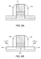
- the Figure 1B illustrates doped areas 25a, 25b under the spacers 13 which have been poorly defined insofar as they extend into the semiconductor region provided for the channel, opposite the gate. These doped zones 25a, 25b thus encroach on the channel zone.
- one solution could consist in making the doped areas under the spacers by implantation.
- Implant doping is also problematic when the semiconductor layer that is to be doped is based on a material different from that of the semiconductor regions formed by epitaxy on either side of the gate.
- this material is intended to induce a stress
- the implantation can cause a relaxation of this stress.
- Such a method makes it possible to define doped zones on either side of the channel region and penetrating under the spacers while limiting the number of steps implemented, in particular photolithography steps.
- This method also makes it possible to precisely define doped zones penetrating under the spacers without impinging on the channel region.
- Such a method also makes it possible to form doped semiconductor zones under the spacers and in contact with the channel zone, without necessarily having to carry out an implantation under the spacers to carry out this doping.
- the semiconductor material formed in the cavities and penetrating beneath the spacers may be adapted to exert stress. In this case, such a method makes it possible to apply this constraint as close as possible to the channel.
- this semiconductor material is different from that of said given region and chosen so as to be able to stretch the atoms of the material of said given region beyond their ordinary interatomic distance.
- Formation of the semiconductor material in the cavities may comprise at least one epitaxial growth step.
- said semiconductor material formed is then doped during growth by epitaxy in the cavities. During this or these epitaxy (s), an in situ doping of said semiconductor material is thus performed.
- said sacrificial zones are based on a sacrificial material, designed to be etched selectively with respect to the rest of said semiconductor layer.
- This sacrificial material may be semiconductor.
- the semiconductor layer may for example be based on Si, while the sacrificial zones are based on SiGe.
- the semiconductor layer may be based on Si x Ge y
- the sacrificial zones may be based on Si a Ge b with b> y.
- these may be zones of a semiconductor layer based on crystalline semiconductor material that has been rendered amorphous.
- the insulating spacers are formed by deposition of dielectric material and preferably after these sacrificial zones, the thermal budget of this deposit being chosen so as to maintain the amorphous nature of the sacrificial zones or so as to induce recrystallization only of a very small thickness of sacrificial areas.
- the deposition temperature and the duration of the deposition are chosen to be lower respectively than a threshold temperature and a threshold duration which depend on the semiconductor material of the sacrificial zones.
- the insulating spacers can be formed directly in contact with the grid.
- the gate comprises a metal zone
- the source and drain regions are made so as to be raised with respect to the channel region. "Raised” means that the source and drain regions are disposed on either side of the gate and extend at least partially above said semiconductor layer in which the channel region is provided.
- a microelectronic device obtained using a method as defined above is also provided.
- the starting material of this process may be a semiconductor-on-insulator type substrate, for example of the SOI type (SOI for "silicon on insulator”), which comprises a semiconductor support layer (not shown) on and in contact with an insulating layer (not shown) which may be based on silicon oxide and disposed on and in contact with the support layer.
- SOI semiconductor on insulator
- the substrate also comprises a thin semiconductor layer 103 located on and in contact with said insulating layer.
- This thin semiconductor layer 103 may have a thickness for example less than 20 nm and which may be for example of the order of 12 nm.
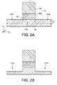
- Deposition steps of a gate dielectric layer 107 and one or more layers 108, 109 of gate material (x), then etching of these layers to realize a transistor gate pattern 110 are then performed ( Figure 2A ).
- the gate 110 of this transistor may be formed of a stack of a metal layer, for example based on TiN, on which a semiconductor layer, for example based on polysilicon, is based.
- a step is taken to remove blocks 103a, 103b of the thin semiconductor layer 103 located on the part of a region 103c of this thin semiconductor layer 103 arranged opposite the gate 107 and provided to form a channel zone of the transistor.
- This shrinkage can be achieved by means of anisotropic etching, for example using HCl, and makes it possible to form cavities 112a, 112b disposed around the region 103c delimiting the channel region of the transistor ( Figure 2B ).
- the etched thickness of the thin conductive layer 103 to form cavities 112a, 112b may be less than the total thickness of this thin conductive layer 103, and for example of the order of 6 to 9 nm. Thus, under the cavities 112a, 112b, a portion of the thin semi-conducting layer 103 is preserved.
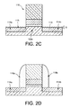
- the cavities 112a, 112b are then filled with a sacrificial material 113, so as to form sacrificial zones 114a, 114b on either side of the grid 110, which are intended to be removed later.
- the thickness of the zones 114a, 114b is provided sacrificial preferably smaller than e 1 blocks 103a, 103b of the thin semiconductor layer 103 that were previously removed.
- the upper face of the thin conductive layer 103 on which the gate dielectric and the gate 110 rests slightly protrude above the upper faces 115 of the sacrificial zones 114a, 114b ( Figure 2C ).
- a deviation or an excess length ⁇ for example of the order of 1 nm or 2 nm may for example be provided, in order to avoid subsequent short-circuiting between the gate and the source and drain zones.
- the sacrificial filling material 113 is preferably a material selected to be selectively etchable to that of the thin semiconductor layer 103.
- the sacrificial material 113 may be a semiconductor material. as for example of Si x Ge y with y for example of the order of 0.3.
- the sacrificial material 113 is a semiconductor material, the latter can be formed by epitaxial growth from the thin semiconductor layer 103, which allows precise control of the thickness of the sacrificial zones 114a, 114b. .
- insulating spacers 118a, 118b are formed against the lateral flanks of the grid 110 and which rest on the zones 114a, 114b of sacrificial material 113.
- the zones 114a, 114b of sacrificial material 113 thus serve as a support for the insulating spacers 118a, 118b.
- the insulating spacers 118a, 118b may be made by depositing a layer of dielectric material such as, for example, Si 3 N 4 , of thickness for example of the order of 10 nm, and then by etching of this dielectric material.
- the zones 114a, 114b are then removed from under the spacers 118a, 118b, preferably using a selective and isotropic etching of the sacrificial material 113 with respect to that of the thin semi-layer. -conductor 103 ( figure 2E ).
- the thin semi-conducting layer 103 is based on Si and the sacrificial material 113 is SiGe, a selective etching with HCl may for example be carried out.
- Cavities 122a, 122b are thus obtained again around the channel zone 103c, these new cavities 122a, 122b being here also arranged so as to extend under the insulating spacers 118a, 118b.
- the cavities 122a, 122b penetrating under the insulating spacers 118a, 118b are then filled with a semiconductor material 123, so as to form source and drain semiconductor blocks 124a, 124b. ( figure 2F ).
- the semiconductor material 123 may be doped, so that zones 125a, 125a doped with blocks 124a, 124b which lie below the spacers 118a, 118b are formed on either side of the channel region 103c of the transistor.
- the semiconductor blocks 124a, 124b are produced using one or more successive epitaxy (s) of semiconductor material which is grown from the remaining thickness of the thin semi-layer. -conductor 103.
- epitaxy or epitaxies an in-situ doping of the semiconductor blocks 124a, 124b is realized.
- the semiconductor blocks 124a, 124b may have a height or thickness e 2 greater than that e 1 of the zones 103a, 103b of the thin semiconductor layer 103 which have been removed previously (the thicknesses e 1 and e 2 being measured in a direction parallel to the z-axis of the orthogonal reference [O, x, y, z] indicated on the Figures 2A and 2 F ).
- the semiconductor blocks 124a, 124b protrude from the upper face of the channel area 103c.
- the doped semiconductor blocks 124a, 124b thus extend above the upper face of the thin semiconductor layer 103 and comprise a portion which extends below the spacers 118a, 118b.
- Drained source and drain regions are thus made which are raised relative to the channel zone 103c on which the gate 110 of the transistor rests, and penetrate under the spacers 118a, 118b so as to be in contact with lateral faces of the transistor. the channel area 103c.
- the semiconductor material 123 of the blocks 124a, 124b can be adapted to induce a compressive stress on the channel region 103c of the transistor.
- the semiconductor material 123 for filling the cavities may be, for example based on silicon-germanium, and doped, in particular to the boron.
- the semiconductor material 123 of the blocks 124a, 124b can be adapted to induce a voltage stress on the channel region 103c of the transistor.
- the semiconductor material 123 formed against the channel zone may be, for example, based on SiC, and doped, in particular with phosphorus.
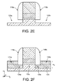
- sacrificial zones are formed by rendering certain regions of the thin semiconductor layer 103 amorphous.
- the grid 110 after having formed the grid 110, it is possible to implement an implantation of the layer 103 which may for example be based on crystalline Si, and in particular on the blocks 103a, 103b of the thin semiconductor layer 103 another of a region 103c of this thin semiconductor layer 103 disposed opposite the gate 107 and provided to form a channel region of the transistor.
- the layer 103 which may for example be based on crystalline Si, and in particular on the blocks 103a, 103b of the thin semiconductor layer 103 another of a region 103c of this thin semiconductor layer 103 disposed opposite the gate 107 and provided to form a channel region of the transistor.
- This amorphous implantation of the blocks 103a, 103b of semiconductor material can be achieved through a masking 200 formed on the gate 110, and with the aid of a non-doping species such as for example Ge or Si.
- sacrificial amorphous zones 214a, 214b are obtained which are to be removed later.
- insulating spacers 118a, 118b are formed against the lateral flanks of the gate 110 and which rest on the sacrificial zones 214a, 214b of amorphous semi-conductor material.
- the insulating spacers 118a, 118b may be formed by a deposit whose thermal budget, in particular the time / temperature pair, is chosen sufficiently small not to induce recrystallization or for inducing a superficial recrystallization of the sacrificial zones 214a, 214b with a thickness of at most 2 nm.
- the maximum thermal budget for not recrystallizing access can be determined from the reference: O. Hellman et al. Materials Science and Engineering: R Reports volume 16 issue 1, 1996 p1-42
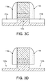
- a selective removal of the sacrificial zones 214a, 214b is first effected.
- This shrinkage can be achieved for example by etching with HCl when the layer 103 is based on crystalline Si and the zones 214a, 214b are based on amorphous Si.
- the cavities 122a, 122b which extend below the spacers 118, 118b and on either side of the channel zone 103c are thus obtained ( 3D figure ).
- cavities 122a, 122b are then filled with a doped semiconductor material 123 and / or adapted to induce a stress on the channel zone 103c.
- semiconductor blocks 124a, 124b are formed, source and drain, raised ( figure 3E ).
- the channel 303c of this transistor may be provided in a semiconductor layer 303 based on Si x Ge y on which the gate 110 is realized.
- Sacrificial zones 314a, 314b based on Si a Ge b can then be formed on either side of the grid 110 with b> y and a ⁇ x ( Figure 4A ), then spacers 118a, 118b are made on these areas 114a, 114b ( Figure 4A ).
- Selective sacrificial zones 314a, 314b based on Si a Ge b can then be selectively etched with the layer 303 of Si x Ge y having a higher Ge concentration than that of these zones, so that in particular, forming the cavities 122a, 122b under the spacers 118a, 118b without etching the channel zone.
- This etching can be carried out for example using HCl, at low temperature, for example less than 700 ° C.
- the source and drain zones can be formed, for example as previously described in connection with the figure 2F by epitaxially growing in the cavities 122a, 122b of a semiconductor material 123 in contact with the channel region 303c and penetrating under the spacers 118a, 118b, this semiconductor material being doped and / or adapted to induce a constrained to the channel region 303c of the transistor.
- These masking zones 509a, 509b are made for example by deposition of a dielectric material, then etching of this dielectric material on the accesses.
- the masking areas 509a, 509b may have a thickness d 1 (measured in a parallel direction [O, x, y] of the orthogonal reference [O, x, y, z] indicated on the Figure 5A ) very low, for example, less than 5 nm or for example between 1 and 4 nm.
- the masking zones 509a, 509b may be provided to avoid possible contamination by equipment metal (s) used during the process, in particular equipment (s) for epitaxy.
- the cavities 112a, 112b are formed on either side of the gate 110 and the channel region of the transistor.
- the sacrificial zones 114a, 114b are produced by epitaxial growth of semiconductor material in the cavities 112a, 112b.
- the insulating spacers 118a, 118b of thickness d 2 > d 1 (d 2 being also measured in a parallel direction [O, x, y] of the orthogonal reference [O, x, y, z] indicated on the Figure 5A ) covering the masking areas 509a, 509b ( Figure 5C ).
- a growth of semiconductor material 123 is carried out in the cavities 122a, 122b so as to form blocks 124a, 124b based on semiconductor material doped and / or adapted to exert a penetrating stress under the spacers 118a, 118b and in contact with the channel region 103c of the transistor.
- a process different from that described above in connection with the Figures 3A-3E provides to make spacers 118a, 118b against the flanks of the gate 110 of the transistor ( Figure 6A ), prior to the realization of sacrificial zones.
- the sacrificial zones 214a, 214b are then formed by amorphous regions located on either side of the channel region 103c of the transistor and penetrating under the spacers 118a, 118b.
- an amorphous implantation is carried out ( Figure 6B ) by means of an inclined beam producing an angle ⁇ , non-zero with respect to a normal n to the main plane of the substrate, for example between 20 ° and 50 °, for example of the order of 45 °.
- the implantation may be carried out for example using Germanium in a dose ranging from 4 to 8 ⁇ 10 14 cm -2 at energies of between 3 and 8 keV.
- This example of implantation can be provided in particular for a silicon zone 12 nm thick where it is desired to amorphize a thickness of 9 nm of an access zone next to the spacers and 6 nm under the spacers to form the sacrificial zones 214a, 214b.
- a method according to the invention can be applied to the implementation of different types of transistor structures and in particular to the production of a transistor comprising a channel structure formed of one or more semiconductor bars.
- S such as MIGFET transistors (for "Multiple Independent Gate Field Effect Transistor"), for example transistors of type commonly called finFET or tri-gate whose gate can extend in several different planes.
Abstract
Procédé de réalisation d'un transistor comprenant des étapes de : - formation de zones sacrificielles (114a, 114b) dans une couche semi-conductrice (103), de part et d'autre d'une région de canal d'un transistor, - formation sur lesdites zones sacrificielles (114a, 114b,) d'espaceurs isolants (118a, 118b) contre des flancs de la grille dudit transistor, - retrait desdites zones sacrificielles de manière à former des cavités (122a, 122b), les cavités s'étendant de part et d'autre de ladite région de canal et pénétrant sous lesdits espaceurs (118a, 118b), - formation de matériau semi-conducteur dopé (123) dans lesdites cavités, ledit matériau semi-conducteur pénétrant sous lesdits espaceurs (118a, 118b).Method of producing a transistor comprising steps of: forming sacrificial zones (114a, 114b) in a semiconductor layer (103), on either side of a channel region of a transistor, forming on said sacrificial zones (114a, 114b) of insulating spacers (118a, 118b) against flanks of the gate of said transistor, removing said sacrificial zones so as to form cavities (122a, 122b), the cavities extending on either side of said channel region and penetrating under said spacers (118a, 118b), forming doped semiconductor material (123) in said cavities, said semiconductor material penetrating under said spacers (118a, 118b).
Description
Le transistor à effet de champ MOS est basé sur une modulation de la concentration de charges dans une région de canal par le biais d'une électrode de grille située au-dessus du canal et isolée de toutes les autres régions du dispositif par un diélectrique de grille. Un tel transistor comporte en outre des régions de source et de drain agencées de chaque côté de la région de canal et qui peuvent être formées dans une même couche semi-conductrice que celle dans laquelle se trouve le canal.The MOS field effect transistor is based on a modulation of the charge concentration in a channel region through a gate electrode located above the channel and isolated from all other regions of the device by a dielectric. wire rack. Such a transistor further comprises source and drain regions arranged on each side of the channel region and which can be formed in the same semiconductor layer as that in which the channel is located.
Afin d'améliorer les performances d'un transistor, il est connu de mettre en oeuvre des régions de source et de drain 11, 12 qui sont surélevées, c'est à dire qui sont réalisées au moins en partie dans des régions semi-conductrices qui s'étendent de part et d'autre d'une grille 10, au-dessus d'une couche semi-conductrice 7 dans laquelle un canal 8 est formé (
Les régions de source 11 et de drain 12 surélevées sont généralement formées par croissance épitaxiale durant laquelle elles peuvent être dopées.The raised
Des espaceurs isolants 13a et 13b agencés contre les flancs latéraux de la grille sont prévus entre la grille 10 et les régions de source 11 et de drain 12.Insulating
Afin de limiter la résistance entre la zone de canal et les régions de source et de drain, on cherche à doper des zones 15a, 15b de la couche semi-conductrice 7 situées sous les espaceurs et qui se trouvent à la frontière de la zone de canal.In order to limit the resistance between the channel zone and the source and drain regions, it is sought to doping
Le dopage de ces zones 15a, 15b peut comprendre un recuit thermique effectué après l'étape d'épitaxie des régions de source et de drain.The doping of these
Cette étape de recuit thermique pose problème dans la mesure où elle nécessite un budget thermique important.This thermal annealing step is problematic in that it requires a significant thermal budget.
Dans le cadre de procédés de fabrication de transistors à basse température, c'est-à-dire au moins inférieure à 700°C, le dopage des zones 15a 15b, est ainsi généralement réalisé par implantation suivi également d'un recuit thermique, mais nécessitant un budget thermique plus faible.In the context of low temperature transistor manufacturing processes, that is to say at least less than 700 ° C, the doping of the
Ce recuit doit de préférence être mené de manière à ne pas doper la zone de canal.This annealing should preferably be conducted so as not to dope the channel area.
La
Pour éviter un empiétement trop important (communément appelé « overlap » selon la terminologie anglo-saxonne), une solution pourrait consister à réaliser les zones dopées sous les espaceurs par implantation.To avoid excessive encroachment (commonly called "overlap" in the English terminology), one solution could consist in making the doped areas under the spacers by implantation.
Cependant cette solution peut alors nécessiter la mise en oeuvre d'étape(s) de photolithographie(s) supplémentaire(s).However, this solution may then require the implementation of additional photolithography step (s).
Un dopage par implantation pose également problème lorsque la couche semi-conductrice que l'on cherche à doper est à base d'un matériau différent de celui des régions semi-conductrices formées par épitaxie de part et d'autre de la grille.Implant doping is also problematic when the semiconductor layer that is to be doped is based on a material different from that of the semiconductor regions formed by epitaxy on either side of the gate.
Lorsque ce matériau est prévu pour induire une contrainte, l'implantation peut entrainer une relaxation de cette contrainte.When this material is intended to induce a stress, the implantation can cause a relaxation of this stress.
Il se pose le problème de trouver un nouveau procédé, de réalisation d'un transistor ayant de meilleures performances et, amélioré vis-à-vis des inconvénients mentionnés ci-dessus.There is the problem of finding a new method, making a transistor with better performance and improved with respect to the disadvantages mentioned above.
Un mode de réalisation de la présente invention prévoit un procédé de réalisation d'un dispositif microélectronique à transistor(s) comprenant des étapes de :
- formation de zones sacrificielles dans une couche semi-conductrice, les zones sacrificielles étant réalisées de part et d'autre d'une région donnée de cette couche semi-conductrice dans laquelle un canal d'un transistor est apte à être formé,
- formation contre une grille dudit transistor reposant sur ladite région donnée, d'espaceurs isolants reposant sur lesdites zones sacrificielles,
- retrait desdites zones sacrificielles de manière à former des cavités, les cavités s'étendant de part et d'autre de ladite région donnée sous lesdits espaceurs,
- formation d'un matériau semi-conducteur dans lesdites cavités et pénétrant sous les espaceurs, le matériau semi-conducteur formé dans les cavités et pénétrant sous les espaceurs étant dopé.
- forming sacrificial zones in a semiconductor layer, the sacrificial zones being formed on either side of a given region of this semiconductor layer in which a channel of a transistor is able to be formed,
- forming against a gate of said transistor resting on said given region, insulating spacers resting on said sacrificial zones,
- removing said sacrificial zones so as to form cavities, the cavities extending on either side of said given region under said spacers,
- forming a semiconductor material in said cavities and penetrating under the spacers, the semiconductor material formed in the cavities and penetrating the spacers being doped.
Un tel procédé permet de définir des zones dopées de part et d'autre de la région de canal et pénétrant sous les espaceurs tout en limitant le nombre d'étapes mises en oeuvre, en particulier d'étapes de photolithographie.Such a method makes it possible to define doped zones on either side of the channel region and penetrating under the spacers while limiting the number of steps implemented, in particular photolithography steps.
Ce procédé permet également de définir précisément des zones dopées pénétrant sous les espaceurs sans empiéter sur la région de canal.This method also makes it possible to precisely define doped zones penetrating under the spacers without impinging on the channel region.
Un tel procédé permet également de former des zones semi-conductrices dopées sous les espaceurs et en contact avec la zone de canal, sans nécessairement devoir réaliser une implantation sous les espaceurs pour effectuer ce dopage.Such a method also makes it possible to form doped semiconductor zones under the spacers and in contact with the channel zone, without necessarily having to carry out an implantation under the spacers to carry out this doping.
Le matériau semi-conducteur formé dans les cavités et pénétrant sous les espaceurs peut être adapté pour exercer une contrainte. Dans ce cas, un tel procédé permet d'appliquer cette contrainte au plus près du canal.The semiconductor material formed in the cavities and penetrating beneath the spacers may be adapted to exert stress. In this case, such a method makes it possible to apply this constraint as close as possible to the channel.
Par matériau adapté pour induire une contrainte, on entend que ce matériau semi-conducteur est différent de celui de ladite région donnée et choisi de manière à pouvoir étirer les atomes du matériau de ladite région donnée au-delà de leur distance interatomique ordinaire.By material adapted to induce a stress is meant that this semiconductor material is different from that of said given region and chosen so as to be able to stretch the atoms of the material of said given region beyond their ordinary interatomic distance.
La formation du matériau semi-conducteur dans les cavités peut comprendre au moins une étape de croissance par épitaxie.Formation of the semiconductor material in the cavities may comprise at least one epitaxial growth step.
Avantageusement, ledit matériau semi-conducteur formé est alors dopé lors de la croissance par épitaxie dans les cavités. On réalise ainsi pendant cette ou ce(s) épitaxie(s), un dopage in situ dudit matériau semi-conducteur.Advantageously, said semiconductor material formed is then doped during growth by epitaxy in the cavities. During this or these epitaxy (s), an in situ doping of said semiconductor material is thus performed.
De préférence, lesdites zones sacrificielles sont à base d'un matériau sacrificiel, prévu pour pouvoir être gravé de manière sélective vis-à-vis du reste de ladite couche semi-conductrice. Ce matériau sacrificiel peut être semi-conducteur.Preferably, said sacrificial zones are based on a sacrificial material, designed to be etched selectively with respect to the rest of said semiconductor layer. This sacrificial material may be semiconductor.
Selon une première possibilité de mise en oeuvre des zones sacrificielles, celles-ci peuvent être réalisées par :
- formation dans la couche semi-conductrice de cavités de part et d'autre de la grille dudit transistor,
- remplissage des cavités à l'aide d'un matériau sacrificiel.
- formation in the semiconductor layer of cavities on either side of the gate of said transistor,
- filling the cavities with a sacrificial material.
La couche semi-conductrice peut être par exemple à base de Si, tandis que les zones sacrificielles sont à base de SiGe.The semiconductor layer may for example be based on Si, while the sacrificial zones are based on SiGe.
En variante, la couche semi-conductrice peut être à base de SixGey, tandis que les zones sacrificielles sont à base de SiaGeb avec b > y.As a variant, the semiconductor layer may be based on Si x Ge y , whereas the sacrificial zones may be based on Si a Ge b with b> y.
Selon une deuxième possibilité de mise en oeuvre des zones sacrificielles, celles-ci peuvent être des zones d'une couche semi-conductrice à base de matériau semi-conducteur cristallin que l'on a rendues amorphes.According to a second possibility of implementing the sacrificial zones, these may be zones of a semiconductor layer based on crystalline semiconductor material that has been rendered amorphous.
Dans ce cas, les espaceurs isolants sont formés par dépôt de matériau diélectrique et de préférence après ces zones sacrificielles, le budget thermique de ce dépôt étant choisi de manière à conserver le caractère amorphe des zones sacrificielles ou de manière à induire une recristallisation seulement d'une épaisseur très faible de zones sacrificielles.In this case, the insulating spacers are formed by deposition of dielectric material and preferably after these sacrificial zones, the thermal budget of this deposit being chosen so as to maintain the amorphous nature of the sacrificial zones or so as to induce recrystallization only of a very small thickness of sacrificial areas.
En particulier, la température de dépôt et la durée du dépôt sont choisies inférieures respectivement à une température seuil et à une durée seuil qui dépendent du matériau semi-conducteur des zones sacrificielles.In particular, the deposition temperature and the duration of the deposition are chosen to be lower respectively than a threshold temperature and a threshold duration which depend on the semiconductor material of the sacrificial zones.
Les espaceurs isolants peuvent être formés directement en contact de la grille.The insulating spacers can be formed directly in contact with the grid.
Selon une mise en oeuvre particulière du procédé dans laquelle la grille comprend une zone métallique, préalablement à la formation des zones sacrificielles, on peut réaliser des zones de protection contre la grille recouvrant ladite zone métallique.According to a particular implementation of the method in which the gate comprises a metal zone, prior to the formation of the sacrificial zones, it is possible to provide protection zones against the gate covering said metal zone.
On peut éviter ainsi une contamination du ou des équipements dans lequel ou dans lesquels on réalise l'étape de formation du matériau semi-conducteur sacrificiel dans les cavités.It is thus possible to avoid contamination of the equipment or equipment in which or in which the step of forming the sacrificial semiconductor material in the cavities is carried out.
Avantageusement, les régions de source et de drain sont réalisées de manière à être surélevées par rapport à la région de canal. Par « surélevées » on entend que les régions de source et de drain sont disposées de part et d'autre de la grille et s'étendent au moins partiellement au-dessus de ladite couche semi-conductrice dans laquelle la région de canal est prévue.Advantageously, the source and drain regions are made so as to be raised with respect to the channel region. "Raised" means that the source and drain regions are disposed on either side of the gate and extend at least partially above said semiconductor layer in which the channel region is provided.
Un dispositif microélectronique obtenu à l'aide d'un procédé tel que défini plus haut est également prévu.A microelectronic device obtained using a method as defined above is also provided.
La présente invention sera mieux comprise à la lecture de la description d'exemples de réalisation donnés, à titre purement indicatif et nullement limitatif, en faisant référence aux dessins annexés sur lesquels :
- les
figures 1A-1B illustrent une réalisation, suivant l'art antérieur, de zones dopées sous les espaceurs isolants d'un transistor MOS ; - les
figure 2A-2F illustrent un exemple de procédé, suivant un mode de réalisation de l'invention, de mise en oeuvre d'un transistor dans lequel on forme sous les espaceurs du transistor un matériau semi-conducteur dopé et/ou adapté pour induire une contrainte par remplissage de cavités réalisées préalablement sous ces espaceurs ; - les
figures 3A-3E illustrent une variante de procédé de réalisation d'un transistor dans laquelle on forme des cavités sous les espaceurs du transistor par gravure de zones d'un matériau semi-conducteur rendu amorphe puis on remplit ces cavités par un matériau semi-conducteur dopé et/ou adapté pour exercer une contrainte, et qui est disposé en contact avec la zone de canal du transistor ; - les
figures 4A-4B illustrent une autre variante de procédé de réalisation de transistor dans laquelle des cavités sont formées sous les espaceurs du transistor par gravure sélective de zones sacrificielles à base d'un matériau semi-conducteur vis-à-vis d'un autre matériau semi-conducteur, puis remplies par un matériau semi-conducteur dopé et/ou adapté pour exercer une contrainte sur le canal du transistor; - les
figures 5A-5C , illustrent une autre variante de procédé dans laquelle des zones de protection sont réalisées sur une zone métallique de la grille d'un transistor préalablement à la réalisation d'espaceurs isolants ; - les
figures 6A-6B , illustrent un autre procédé, de fabrication d'un transistor dans lequel, après avoir réalisé des espaceurs, on forme de zones sacrificielles sous ces espaceurs qui sont destinées à être retirées ultérieurement pour former des cavités;
- the
Figures 1A-1B illustrate an embodiment, according to the prior art, of doped areas under the insulating spacers of a MOS transistor; - the
Figure 2A-2F illustrate an example of a method, according to one embodiment of the invention, of implementation of a transistor in which is formed under the spacers of the transistor a semiconductor material doped and / or adapted to induce a stress by filling of cavities previously made under these spacers; - the
Figures 3A-3E illustrate an alternative method of producing a transistor in which cavities are formed under the spacers of the transistor by etching zones of an amorphous semi-conducting material and then filling these cavities with a doped semiconductor material and / or adapted to exert a stress, and which is disposed in contact with the channel region of the transistor; - the
Figures 4A-4B illustrate another variant of a transistor manufacturing method in which cavities are formed under the spacers of the transistor by selective etching sacrificial zones based on a semiconductor material vis-à-vis another semiconductor material, then filled with a semiconductor material doped and / or adapted to exert a stress on the channel of the transistor; - the
Figures 5A-5C , illustrate another variant of the method in which protection zones are formed on a metal zone of the gate of a transistor prior to the production of insulating spacers; - the
Figures 6A-6B , illustrate another method of manufacturing a transistor in which, after forming spacers, forming sacrificial zones under these spacers which are intended to be removed later to form cavities;
Des parties identiques, similaires ou équivalentes des différentes figures portent les mêmes références numériques de façon à faciliter le passage d'une figure à l'autre.Identical, similar or equivalent parts of the different figures bear the same numerical references so as to facilitate the passage from one figure to another.
Les différentes parties représentées sur les figures ne le sont pas nécessairement selon une échelle uniforme, pour rendre les figures plus lisibles.The different parts shown in the figures are not necessarily in a uniform scale, to make the figures more readable.
Un exemple de procédé, suivant l'invention, de réalisation d'un dispositif micro-électronique à transistor(s) va à présent être décrit en liaison avec les
Le matériau de départ de ce procédé peut être un substrat de type semi-conducteur sur isolant par exemple de type SOI (SOI pour « silicium sur isolant ») qui comprend une couche de support semi-conducteur (non représentée) sur et en contact avec une couche isolante (non représentée) qui peut être à base d'oxyde de silicium et disposée sur et en contact avec la couche de support. Le substrat comporte également une fine couche semi conductrice 103 située sur et en contact avec ladite couche isolante.The starting material of this process may be a semiconductor-on-insulator type substrate, for example of the SOI type (SOI for "silicon on insulator"), which comprises a semiconductor support layer (not shown) on and in contact with an insulating layer (not shown) which may be based on silicon oxide and disposed on and in contact with the support layer. The substrate also comprises a
Cette fine couche semi conductrice 103 peut avoir une épaisseur par exemple inférieure à 20 nm et qui peut être par exemple de l'ordre de 12 nm.This
Des étapes de dépôt d'une couche de diélectrique 107 de grille et d'une ou plusieurs couches 108, 109 de matériau(x) de grille, puis de gravure de ces couches afin de réaliser un motif de grille 110 de transistor sont ensuite effectuées (
La grille 110 de ce transistor peut être formée d'un empilement d'une couche métallique, par exemple à base de TiN, sur laquelle repose une couche semi-conductrice, par exemple à base de polysilicium.The
Puis, on effectue une étape de retrait de blocs 103a, 103b de la fine couche semi conductrice 103 situés de part d'une région 103c de cette fine couche semi conductrice 103 disposée en regard de la grille 107 et prévue pour former une zone de canal du transistor.Then, a step is taken to remove
Ce retrait peut être réalisé à l'aide d'une gravure anisotrope, par exemple à l'aide de HCl et permet de former des cavités 112a, 112b disposées autour de la région 103c délimitant la zone de canal du transistor (
L'épaisseur gravée de la fine couche conductrice 103 pour former des cavités 112a, 112b peut être inférieure à l'épaisseur totale de cette fine couche conductrice 103, et par exemple de l'ordre de 6 à 9 nm. On conserve ainsi, sous les cavités 112a, 112b, une portion de la fine couche semi-conductrice 103.The etched thickness of the thin
On comble ensuite les cavités 112a, 112b à l'aide d'un matériau sacrificiel 113, de manière à former des zones 114a, 114b sacrificielles de part et d'autre de la grille 110, qui sont destinées à être retirées ultérieurement.The
L'épaisseur des zones 114a, 114b sacrificielles est prévue de préférence Inférieure à celle e1 des blocs 103a, 103b de la fine couche semi conductrice 103 qui ont été retirées précédemment.The thickness of the
Ainsi, la face supérieure de la fine couche conductrice 103 sur laquelle repose le diélectrique de grille et la grille 110 dépasse légèrement au-dessus des faces supérieures 115 des zones 114a, 114b sacrificielles (
Le matériau sacrificiel 113 de remplissage des cavités est de préférence un matériau choisi de manière à pouvoir être gravé de manière sélective vis-à-vis de celui de la fine couche semi-conductrice 103. Le matériau sacrificiel 113 peut être un matériau semi-conducteur tel que par exemple du SixGey avec y par exemple de l'ordre de 0,3. Lorsque le matériau sacrificiel 113 est un matériau semi-conducteur, on peut former ce dernier par croissance par épitaxie à partir de la fine couche semi-conductrice 103, ce qui permet de réaliser un contrôle précis de l'épaisseur des zones sacrificielles 114a, 114b.The
Ensuite (
Les espaceurs isolants 118a, 118b peuvent être réalisés par dépôt d'une couche de matériau diélectrique tel que par exemple du Si3N4, d'épaisseur par exemple de l'ordre de 10 nm, puis par gravure de ce matériau diélectrique.The insulating
On effectue ensuite un retrait des zones 114a, 114b, et ce jusque sous les espaceurs 118a, 118b, de préférence à l'aide d'une gravure sélective et isotrope du matériau sacrificiel 113 vis-à-vis de celui de la fine couche semi-conductrice 103 (
Dans le cas où la fine couche semi-conductrice 103 est à base de Si et le matériau sacrificiel 113 est du SiGe, une gravure sélective à l'aide de HCl peut être par exemple mise en oeuvre.In the case where the thin
On obtient ainsi à nouveau des cavités 122a, 122b autour de la zone de canal 103c, ces nouvelles cavités 122a, 122b étant ici également agencées de manière à s'étendre sous les espaceurs isolants 118a, 118b.
Les cavités 122a, 122b pénétrant sous les espaceurs isolants 118a, 118b sont ensuite comblé(e)s à l'aide d'un matériau semi-conducteur 123, de manière à former des blocs semi-conducteurs 124a, 124b de source et de drain (
Les blocs semi-conducteurs 124a, 124b sont dans cet exemple réalisés à l'aide d'une ou plusieurs épitaxie(s) successives de matériau semi-conducteur que l'on fait croître à partir de l'épaisseur restante de la fine couche semi-conductrice 103. Lors de l'épitaxie ou des épitaxies, un dopage in-situ des blocs semi-conducteurs 124a, 124b est réalisé.In this example, the
Les blocs semi-conducteurs 124a, 124b peuvent avoir une hauteur ou épaisseur e2 supérieure à celle e1 des zones 103a, 103b de la fine couche semi-conductrice 103 qui ont été retirées précédemment (les épaisseurs e1 et e2 étant mesurées dans une direction parallèle à l'axe z du repère orthogonal [O,x,y,z] indiqué sur les
Les blocs semi-conducteurs 124a, 124b dopés s'étendent ainsi au-dessus de la face supérieure de la fine couche semi conductrice 103 et comportent une portion qui s'étend sous les espaceurs 118a, 118b.The doped
On réalise ainsi des zones de source et de drains dopées qui sont surélevées par rapport à la zone de canal 103c sur laquelle repose la grille 110 du transistor, et pénètrent sous les espaceurs 118a, 118b de manière à être en contact avec des faces latérales de la zone de canal 103c.Drained source and drain regions are thus made which are raised relative to the
Dans un cas où l'on forme un transistor de type PMOS, le matériau semi-conducteur 123 des blocs 124a, 124b peut être adapté pour induire une contrainte en compression sur la zone de canal 103c du transistor. Dans ce cas, le matériau semi-conducteur 123 de remplissage des cavités peut être, par exemple à base de silicium-germanium, et dopé, en particulier au Bore.In a case where a PMOS type transistor is formed, the
Dans un cas où l'on forme un transistor de type NMOS, le matériau semi-conducteur 123 des blocs 124a, 124b peut être adapté pour induire une contrainte en tension sur la zone de canal 103c du transistor. Dans ce cas, le matériau semi-conducteur 123 formé contre la zone de canal peut être, par exemple, à base de SiC, et dopé, en particulier au Phosphore.In a case where an NMOS-type transistor is formed, the
Une variante de l'exemple de procédé qui vient d'être décrit est illustrée sur les
Selon cette variante, on forme des zones sacrificielles en rendant amorphes certaine régions de la fine couche semi-conductrice 103.According to this variant, sacrificial zones are formed by rendering certain regions of the
Pour cela, après avoir formé la grille 110, on peut réaliser une implantation de la couche 103 qui peut être par exemple à base de Si cristallin, et en particulier de blocs 103a, 103b de la fine couche semi conductrice 103 situés de part et d'autre d'une région 103c de cette fine couche semi conductrice 103 disposée en regard de la grille 107 et prévue pour former une zone de canal du transistor.For this, after having formed the
Cette implantation amorphisante des blocs 103a, 103b de matériau semi-conducteur peut être réalisée à travers un masquage 200 formé sur la grille 110, et à l'aide d'une espèce non dopante telle que par exemple du Ge ou de Si.This amorphous implantation of the
A l'issue de l'étape d'implantation, on obtient des zones 214a, 214b amorphes sacrificielles destinées à être retirées ultérieurement.At the end of the implantation step, sacrificial
Ensuite (
Afin de conserver le caractère amorphe des zones 214a, 214b sacrificielles, les espaceurs isolants 118a, 118b peuvent être formées par un dépôt dont le budget thermique, en particulier le couple temps/température, est choisi suffisamment faible pour ne pas induire de recristallisation ou pour induire une recristallisation superficielle des zones 214a, 214b sacrificielles d'une épaisseur d'au plus 2 nm.In order to preserve the amorphous nature of the
Par exemple, dans le cas de zones de silicium, on peut prévoir un budget thermique de 500°C avec une durée inférieure à 1 min ou de 450°C avec une durée inférieure à 10 min dans le cas où le matériau de la couche 103 et des zones 214a, 214b est du silicium. Dans le cas par exemple de zones à base de Si ou de SiGe non dopé, le budget thermique maximum pour ne pas recristalliser l'accès peut être déterminé à partir de la référence :
On réalise ensuite des étapes du type de celles données dans l'exemple de procédé décrit précédemment.Steps of the type of those given in the example of the method described above are then carried out.
Ainsi, on effectue tout d'abord un retrait sélectif des zones sacrificielles 214a, 214b. Ce retrait peut être réalisé par exemple par gravure à l'aide de HCl lorsque la couche 103 est à base de Si cristallin et que les zones 214a, 214b sont à base de Si amorphe.Thus, a selective removal of the
On obtient ainsi les cavités 122a, 122b qui s'étendent sous les espaceurs 118, 118b et de part et d'autre de la zone de canal 103c (
Ces cavités 122a, 122b sont ensuite comblées à l'aide d'un matériau semi-conducteur 123 dopé et/ou adapté pour induire une contrainte sur la zone 103c de canal.These
On forme ainsi des blocs semi-conducteurs 124a, 124b, de source et de drain, surélevés (
Selon une autre variante de réalisation, par exemple lorsque le transistor que l'on réalise est de type PMOS, le canal 303c de ce transistor peut être prévu dans une couche semi-conductrice 303 à base de SixGey sur laquelle la grille 110 est réalisée.According to another variant embodiment, for example when the transistor which is made is of the PMOS type, the
Des zones sacrificielles 314a, 314b à base de SiaGeb peuvent alors être formées de part et d'autre de la grille 110 avec b>y et a<x (
On peut ensuite effectuer une gravure sélective des zones sacrificielles 314a, 314b à base de SiaGeb vis-à-vis de la couche 303 de SixGey ayant une concentration en Ge plus élevée que celle de ces zones, de manière à former notamment les cavités 122a, 122b sous les espaceurs 118a, 118b sans graver la zone de canal.Selective
Cette gravure peut être réalisée par exemple à l'aide de HCl, à basse température, par exemple inférieure à 700°C.This etching can be carried out for example using HCl, at low temperature, for example less than 700 ° C.
Ensuite, les zones de source et de drain peuvent être formées, par exemple comme cela été décrit précédemment en liaison avec la
Selon une autre variante de réalisation (
Ces zones 509a, 509b de masquage sont réalisées par exemple par dépôt d'un matériau diélectrique, puis gravure de ce matériau diélectrique sur les accès. Les zones 509a, 509b de masquage peuvent avoir une épaisseur d1 (mesurée dans une direction parallèle [O,x,y] du repère orthogonal [O,x,y,z] indiqué sur la
Les zones 509a, 509b de masquage peuvent être prévues pour éviter une éventuelle contamination par du métal d'équipement(s) utilisé(s) au cours du procédé, en particulier d'équipement(s) d'épitaxie.The
Ensuite, on forme les cavités 112a, 112b de part et d'autre de la grille 110 et de la région de canal du transistor.Then, the
Puis, on réalise les zones 114a, 114b sacrificielles, par croissance par épitaxie de matériau semi-conducteur dans les cavités 112a, 112b.Then, the
Ensuite, on peut former les espaceurs isolants 118a, 118b d'épaisseur d2 > d1 (d2 étant également mesurée dans une direction parallèle [O,x,y] du repère orthogonal [O,x,y,z] indiqué sur la
On peut ensuite effectuer un procédé tel que décrit précédemment en liaison avec les
Puis, on réalise une croissance de matériau semi-conducteur 123 dans les cavités 122a, 122b de manière à former des blocs 124a, 124b à base de matériau semi-conducteur dopé et/ou adapté pour exercer une contrainte pénétrant sous les espaceurs 118a, 118b et en contact avec la région 103c de canal du transistor.Then, a growth of
Un procédé différent de celui décrit précédemment en liaison avec les
On forme ensuite les zones sacrificielles 214a, 214b, en rendant amorphes des régions situées de part et d'autre de la zone de canal 103c du transistor et pénétrant sous les espaceurs 118a, 118b.The
Pour cela, on réalise une implantation amorphisante (
On peut ensuite effectuer des étapes telles que décrites en liaison avec les
Un procédé suivant l'invention peut s'appliquer à la mise en oeuvre de différents types de structures de transistors et en particulier à la réalisation d'un transistor comportant une structure de canal formée d'un ou plusieurs barreau(x) semi-conducteur(s) tel(s) que les transistors MIGFET (pour « Multiple Independent Gate Field Effect Transistor »), par exemple les transistors de type communément appelé finFET ou tri-gate dont la grille peut s'étendre sur plusieurs plans différents.A method according to the invention can be applied to the implementation of different types of transistor structures and in particular to the production of a transistor comprising a channel structure formed of one or more semiconductor bars. (S) such as MIGFET transistors (for "Multiple Independent Gate Field Effect Transistor"), for example transistors of type commonly called finFET or tri-gate whose gate can extend in several different planes.
Claims (10)
Applications Claiming Priority (1)
| Application Number | Priority Date | Filing Date | Title |
|---|---|---|---|
| FR1357931A FR3009651B1 (en) | 2013-08-09 | 2013-08-09 | IMPROVED METHOD FOR MAKING DOPED AREAS AND / OR EXERCISING A STRAIN UNDER THE SPACERS OF A TRANSISTOR |
Publications (2)
| Publication Number | Publication Date |
|---|---|
| EP2835832A2 true EP2835832A2 (en) | 2015-02-11 |
| EP2835832A3 EP2835832A3 (en) | 2015-06-03 |
Family
ID=49237485
Family Applications (1)
| Application Number | Title | Priority Date | Filing Date |
|---|---|---|---|
| EP14180025.0A Withdrawn EP2835832A3 (en) | 2013-08-09 | 2014-08-06 | Improved method for producing doped areas and/or exerting a stress on the spacers of a transistor |
Country Status (3)
| Country | Link |
|---|---|
| US (1) | US9379213B2 (en) |
| EP (1) | EP2835832A3 (en) |
| FR (1) | FR3009651B1 (en) |
Cited By (1)
| Publication number | Priority date | Publication date | Assignee | Title |
|---|---|---|---|---|
| FR3116379A1 (en) * | 2020-11-18 | 2022-05-20 | Commissariat A L'energie Atomique Et Aux Energies Alternatives | Process for manufacturing a doped zone of a microelectronic device |
Families Citing this family (8)
| Publication number | Priority date | Publication date | Assignee | Title |
|---|---|---|---|---|
| US9396984B2 (en) | 2012-09-05 | 2016-07-19 | Commissariat A L'energie Atomique Et Aux Energies Alternatives | Method of producing a microelectronic device in a monocrystalline semiconductor substrate with isolation trenches partially formed under an active region |
| WO2014039034A1 (en) | 2012-09-05 | 2014-03-13 | Commissariat A L'energie Atomique Et Aux Energies Alternatives | Method for fabricating microelectronic devices with isolation trenches partially formed under active regions |
| EP2917930A4 (en) | 2012-11-08 | 2016-06-29 | Commissariat à l'énergie atomique et aux énergies alternatives | Method for fabricating microelectronic devices with isolation trenches partially formed under active regions |
| FR3009648B1 (en) | 2013-08-09 | 2016-12-23 | Commissariat Energie Atomique | RECRYSTALLIZATION OF SOURCE BLOCKS AND DRAIN FROM THE TOP |
| FR3015769B1 (en) | 2013-12-23 | 2017-08-11 | Commissariat Energie Atomique | IMPROVED METHOD FOR PRODUCING CONCEALED SEMICONDUCTOR BLOCKS ON THE INSULATING LAYER OF A SEMICONDUCTOR SUBSTRATE ON INSULATION |
| FR3031835B1 (en) | 2015-01-16 | 2017-12-22 | Commissariat Energie Atomique | METHOD FOR MAKING A THREE DIMENSIONAL INTEGRATED ELECTRONIC CIRCUIT |
| US9768254B2 (en) | 2015-07-30 | 2017-09-19 | International Business Machines Corporation | Leakage-free implantation-free ETSOI transistors |
| FR3047352B1 (en) | 2016-02-02 | 2018-02-09 | Commissariat A L'energie Atomique Et Aux Energies Alternatives | METHOD FOR MANUFACTURING A DOPANT TRANSISTOR LOCATED WITH THE GRIT APLOMB |
Family Cites Families (7)
| Publication number | Priority date | Publication date | Assignee | Title |
|---|---|---|---|---|
| US6881635B1 (en) * | 2004-03-23 | 2005-04-19 | International Business Machines Corporation | Strained silicon NMOS devices with embedded source/drain |
| US7732285B2 (en) * | 2007-03-28 | 2010-06-08 | Intel Corporation | Semiconductor device having self-aligned epitaxial source and drain extensions |
| US7994010B2 (en) * | 2007-12-27 | 2011-08-09 | Chartered Semiconductor Manufacturing Ltd. | Process for fabricating a semiconductor device having embedded epitaxial regions |
| US7838372B2 (en) * | 2008-05-22 | 2010-11-23 | Infineon Technologies Ag | Methods of manufacturing semiconductor devices and structures thereof |
| US8299453B2 (en) * | 2009-03-03 | 2012-10-30 | International Business Machines Corporation | CMOS transistors with silicon germanium channel and dual embedded stressors |
| FR3009648B1 (en) | 2013-08-09 | 2016-12-23 | Commissariat Energie Atomique | RECRYSTALLIZATION OF SOURCE BLOCKS AND DRAIN FROM THE TOP |
| FR3009887B1 (en) | 2013-08-20 | 2015-09-25 | Commissariat Energie Atomique | IMPROVED METHOD OF SEPARATION BETWEEN AN ACTIVE ZONE OF A SUBSTRATE AND ITS REAR FACE OR A PORTION OF ITS BACKFACE |
-
2013
- 2013-08-09 FR FR1357931A patent/FR3009651B1/en active Active
-
2014
- 2014-08-04 US US14/450,385 patent/US9379213B2/en active Active
- 2014-08-06 EP EP14180025.0A patent/EP2835832A3/en not_active Withdrawn
Non-Patent Citations (1)
| Title |
|---|
| 0. HELLMAN ET AL., MATERIALS SCIENCE AND ENGINEERING : R REPORTS, vol. 16, no. 1, 1996, pages 42 |
Cited By (3)
| Publication number | Priority date | Publication date | Assignee | Title |
|---|---|---|---|---|
| FR3116379A1 (en) * | 2020-11-18 | 2022-05-20 | Commissariat A L'energie Atomique Et Aux Energies Alternatives | Process for manufacturing a doped zone of a microelectronic device |
| EP4002486A1 (en) | 2020-11-18 | 2022-05-25 | Commissariat à l'Energie Atomique et aux Energies Alternatives | Method for manufacturing a doped area of a microelectronic device |
| US11942323B2 (en) | 2020-11-18 | 2024-03-26 | Commissariat A L'energie Atomique Et Aux Energies Alternatives | Method for manufacturing a doped zone of a microelectronic device |
Also Published As
| Publication number | Publication date |
|---|---|
| EP2835832A3 (en) | 2015-06-03 |
| US9379213B2 (en) | 2016-06-28 |
| US20150044841A1 (en) | 2015-02-12 |
| FR3009651A1 (en) | 2015-02-13 |
| FR3009651B1 (en) | 2016-12-23 |
Similar Documents
| Publication | Publication Date | Title |
|---|---|---|
| EP2835832A2 (en) | Improved method for producing doped areas and/or exerting a stress on the spacers of a transistor | |
| EP3070744B1 (en) | Improved method for producing a transistor in a stack of superposed semiconductor layers | |
| EP2887384B1 (en) | Improved method for producing stressed semiconductor blocks on the insulating layer of a semiconductor on insulator substrate | |
| FR3060840A1 (en) | METHOD FOR MAKING A SEMICONDUCTOR DEVICE HAVING SELF-ALIGNED INTERNAL SPACERS | |
| EP2840594B1 (en) | Recrystallisation of blocks with source and drain by the top | |
| FR3060838A1 (en) | METHOD FOR PRODUCING A SEMICONDUCTOR DEVICE WITH A COMPRESSION-CONSTANT CHANNEL | |
| FR3060841A1 (en) | METHOD FOR MAKING A SEMICONDUCTOR DEVICE HAVING SELF-ALIGNED INTERNAL SPACERS | |
| EP2975646B1 (en) | Method for manufacturing a transistor in which the level of stress applied to the channel is increased | |
| EP3502048B1 (en) | Method for producing a fet transistor with strained channel | |
| EP3142152B1 (en) | Method for tensioning a semiconductor film | |
| FR3023411A1 (en) | LOCALIZED GENERATION OF STRESS IN A SOIL SUBSTRATE | |
| FR3014244A1 (en) | IMPROVED METHOD FOR PRODUCING A CONDUCTIVE SEMICONDUCTOR SUBSTRATE ON INSULATION | |
| EP3142151B1 (en) | Method for producing an uniaxially stressed transistor channel structure | |
| EP3079168A1 (en) | Method for doping source and drain regions of a transistor by means of selective amorphisation | |
| FR3015768A1 (en) | IMPROVED METHOD OF MODIFYING THE STRAIN STATUS OF A BLOCK OF SEMICONDUCTOR MATERIAL | |
| FR3057703B1 (en) | METHOD FOR MANUFACTURING A COILGROUND FIELD EFFECT TRANSISTOR | |
| EP3026711B1 (en) | Improved method for inducing strain in a transistor channel using sacrificial source/drain regions and a gate replacement | |
| EP3026712B1 (en) | Improved method for straining a region of a transistor channel | |
| FR3057702A1 (en) | METHOD FOR MANUFACTURING A COILGROUND FIELD EFFECT TRANSISTOR | |
| FR3048816A1 (en) | METHOD FOR MANUFACTURING DEVICE WITH VOLTAGE CONSTANT NMOS TRANSISTOR AND PMOS TRANSISTOR CONSTRAINED IN UNI-AXIAL COMPRESSION | |
| EP3062350B1 (en) | Method for modifying the state of stress of a semiconductor structure with transistor channel stages | |
| FR3048815A1 (en) | METHOD FOR CO-REALIZATION OF ZONES UNDER DIFFERENT UNIAXIAL CONSTRAINTS | |
| EP3442027A1 (en) | Method for forming doped extension regions in a structure having stacked nanowires | |
| EP3490007B1 (en) | Method for manufacturing fin-fet type cmos transistor pairs at low temperature | |
| FR3050315B1 (en) | TRANSISTOR A OVERLAP OF MASTER ACCESS REGIONS |
Legal Events
| Date | Code | Title | Description |
|---|---|---|---|
| PUAI | Public reference made under article 153(3) epc to a published international application that has entered the european phase |
Free format text: ORIGINAL CODE: 0009012 |
|
| 17P | Request for examination filed |
Effective date: 20140806 |
|
| AK | Designated contracting states |
Kind code of ref document: A2 Designated state(s): AL AT BE BG CH CY CZ DE DK EE ES FI FR GB GR HR HU IE IS IT LI LT LU LV MC MK MT NL NO PL PT RO RS SE SI SK SM TR |
|
| AX | Request for extension of the european patent |
Extension state: BA ME |
|
| PUAL | Search report despatched |
Free format text: ORIGINAL CODE: 0009013 |
|
| AK | Designated contracting states |
Kind code of ref document: A3 Designated state(s): AL AT BE BG CH CY CZ DE DK EE ES FI FR GB GR HR HU IE IS IT LI LT LU LV MC MK MT NL NO PL PT RO RS SE SI SK SM TR |
|
| AX | Request for extension of the european patent |
Extension state: BA ME |
|
| RIC1 | Information provided on ipc code assigned before grant |
Ipc: H01L 29/66 20060101AFI20150428BHEP |
|
| STAA | Information on the status of an ep patent application or granted ep patent |
Free format text: STATUS: THE APPLICATION IS DEEMED TO BE WITHDRAWN |
|
| 18D | Application deemed to be withdrawn |
Effective date: 20151204 |