EP2835688B1 - Nano-patterned system and magnetic-field applying device thereof - Google Patents
Nano-patterned system and magnetic-field applying device thereof Download PDFInfo
- Publication number
- EP2835688B1 EP2835688B1 EP12873678.2A EP12873678A EP2835688B1 EP 2835688 B1 EP2835688 B1 EP 2835688B1 EP 12873678 A EP12873678 A EP 12873678A EP 2835688 B1 EP2835688 B1 EP 2835688B1
- Authority
- EP
- European Patent Office
- Prior art keywords
- magnetic
- applying device
- field applying
- field
- sample stage
- Prior art date
- Legal status (The legal status is an assumption and is not a legal conclusion. Google has not performed a legal analysis and makes no representation as to the accuracy of the status listed.)
- Active
Links
Images




Classifications
-
- H—ELECTRICITY
- H01—ELECTRIC ELEMENTS
- H01J—ELECTRIC DISCHARGE TUBES OR DISCHARGE LAMPS
- H01J37/00—Discharge tubes with provision for introducing objects or material to be exposed to the discharge, e.g. for the purpose of examination or processing thereof
- H01J37/02—Details
- H01J37/04—Arrangements of electrodes and associated parts for generating or controlling the discharge, e.g. electron-optical arrangement or ion-optical arrangement
- H01J37/09—Diaphragms; Shields associated with electron or ion-optical arrangements; Compensation of disturbing fields
-
- G—PHYSICS
- G01—MEASURING; TESTING
- G01R—MEASURING ELECTRIC VARIABLES; MEASURING MAGNETIC VARIABLES
- G01R33/00—Arrangements or instruments for measuring magnetic variables
- G01R33/02—Measuring direction or magnitude of magnetic fields or magnetic flux
- G01R33/06—Measuring direction or magnitude of magnetic fields or magnetic flux using galvano-magnetic devices
- G01R33/09—Magnetoresistive devices
- G01R33/093—Magnetoresistive devices using multilayer structures, e.g. giant magnetoresistance sensors
-
- G—PHYSICS
- G01—MEASURING; TESTING
- G01R—MEASURING ELECTRIC VARIABLES; MEASURING MAGNETIC VARIABLES
- G01R33/00—Arrangements or instruments for measuring magnetic variables
- G01R33/02—Measuring direction or magnitude of magnetic fields or magnetic flux
- G01R33/06—Measuring direction or magnitude of magnetic fields or magnetic flux using galvano-magnetic devices
- G01R33/09—Magnetoresistive devices
- G01R33/096—Magnetoresistive devices anisotropic magnetoresistance sensors
-
- H—ELECTRICITY
- H01—ELECTRIC ELEMENTS
- H01F—MAGNETS; INDUCTANCES; TRANSFORMERS; SELECTION OF MATERIALS FOR THEIR MAGNETIC PROPERTIES
- H01F41/00—Apparatus or processes specially adapted for manufacturing or assembling magnets, inductances or transformers; Apparatus or processes specially adapted for manufacturing materials characterised by their magnetic properties
-
- H—ELECTRICITY
- H01—ELECTRIC ELEMENTS
- H01F—MAGNETS; INDUCTANCES; TRANSFORMERS; SELECTION OF MATERIALS FOR THEIR MAGNETIC PROPERTIES
- H01F7/00—Magnets
- H01F7/06—Electromagnets; Actuators including electromagnets
- H01F7/20—Electromagnets; Actuators including electromagnets without armatures
- H01F7/202—Electromagnets for high magnetic field strength
-
- H—ELECTRICITY
- H01—ELECTRIC ELEMENTS
- H01F—MAGNETS; INDUCTANCES; TRANSFORMERS; SELECTION OF MATERIALS FOR THEIR MAGNETIC PROPERTIES
- H01F7/00—Magnets
- H01F7/06—Electromagnets; Actuators including electromagnets
- H01F7/20—Electromagnets; Actuators including electromagnets without armatures
- H01F7/202—Electromagnets for high magnetic field strength
- H01F7/204—Circuits for energising or de-energising
-
- H—ELECTRICITY
- H01—ELECTRIC ELEMENTS
- H01J—ELECTRIC DISCHARGE TUBES OR DISCHARGE LAMPS
- H01J37/00—Discharge tubes with provision for introducing objects or material to be exposed to the discharge, e.g. for the purpose of examination or processing thereof
- H01J37/02—Details
- H01J37/04—Arrangements of electrodes and associated parts for generating or controlling the discharge, e.g. electron-optical arrangement or ion-optical arrangement
- H01J37/10—Lenses
- H01J37/14—Lenses magnetic
- H01J37/141—Electromagnetic lenses
-
- H—ELECTRICITY
- H10—SEMICONDUCTOR DEVICES; ELECTRIC SOLID-STATE DEVICES NOT OTHERWISE PROVIDED FOR
- H10N—ELECTRIC SOLID-STATE DEVICES NOT OTHERWISE PROVIDED FOR
- H10N50/00—Galvanomagnetic devices
- H10N50/01—Manufacture or treatment
-
- H—ELECTRICITY
- H01—ELECTRIC ELEMENTS
- H01J—ELECTRIC DISCHARGE TUBES OR DISCHARGE LAMPS
- H01J2237/00—Discharge tubes exposing object to beam, e.g. for analysis treatment, etching, imaging
- H01J2237/02—Details
- H01J2237/026—Shields
- H01J2237/0262—Shields electrostatic
-
- H—ELECTRICITY
- H01—ELECTRIC ELEMENTS
- H01J—ELECTRIC DISCHARGE TUBES OR DISCHARGE LAMPS
- H01J2237/00—Discharge tubes exposing object to beam, e.g. for analysis treatment, etching, imaging
- H01J2237/02—Details
- H01J2237/026—Shields
- H01J2237/0264—Shields magnetic
-
- H—ELECTRICITY
- H01—ELECTRIC ELEMENTS
- H01J—ELECTRIC DISCHARGE TUBES OR DISCHARGE LAMPS
- H01J2237/00—Discharge tubes exposing object to beam, e.g. for analysis treatment, etching, imaging
- H01J2237/26—Electron or ion microscopes
- H01J2237/28—Scanning microscopes
-
- H—ELECTRICITY
- H01—ELECTRIC ELEMENTS
- H01J—ELECTRIC DISCHARGE TUBES OR DISCHARGE LAMPS
- H01J2237/00—Discharge tubes exposing object to beam, e.g. for analysis treatment, etching, imaging
- H01J2237/30—Electron or ion beam tubes for processing objects
- H01J2237/317—Processing objects on a microscale
- H01J2237/3175—Lithography
- H01J2237/31752—Lithography using particular beams or near-field effects, e.g. STM-like techniques
- H01J2237/31754—Lithography using particular beams or near-field effects, e.g. STM-like techniques using electron beams
Definitions
- the present invention relates to a nano-patterning and magneto-electric high-frequency characteristic measurement system, and particularly to a micro/nano-patterning system for measuring and studying the magneto-electric response characteristics of a micro/nano-patterning device as well as a magnetic-field applying device thereof.
- GMR Giant Magnetoresistance
- TMR Tunneling Magnetoresistance
- Electron Beam Lithography (EBL) System is one of the important equipment for integration of the preparation and observation of nanostructures. It comprises a scanning electron microscopy (SEM) imaging function and an electron beam pattern generator, i.e. it writes nano-patterns directly on a resist layer using a focused electron beam. As the electron beam is characterized by a small beam spot and high energy, nanostructures with a line width of 5 to 10 nm can be produced by using an EBL system. This is the ideal method for making nano materials and devices.
- the world record of the production of nanostructures with a minimum line width of less than 5 nm was set by Raith GmbH (Germany) and has been held by it so far.
- US patent US 20040173755A1 recorded an electron-beam focusing apparatus for controlling a path of electron beams emitted from an electron-beam emitter in an electron-beam projection lithography (EPL) system includes top and bottom magnets for creating a magnetic field within a vacuum chamber, the top and bottom magnets disposed above and below the vacuum chamber into which a wafer is loaded, respectively; upper and lower pole pieces magnetically contacting the top and bottom magnets, respec-tively, the upper and lower pole pieces penetrating a top wall and a bottom wall of the vacuum chamber, respectively; and upper and lower projections having a circular shape, extend-ing outwardly from facing surfaces of the upper and lower pole pieces, respectively.
- EPL electron-beam projection lithography
- US patent US 5900728 recorded an alternating current (AC) magnetic force microscopy (MFM) system incorporates an improved probe with an integrated coil on the free end of the system's cantilever.
- the probe has a pair of magnetic poles that form part of a magnetic yoke and a patterned electrically conductive coil wound through the yoke.
- the probe includes a probe tip that has a magnetic surface layer that is magnetically coupled to one of the poles and extends from it.
- alternating current from the AC-MFM system is passed through the probe coil the magnetization direction of the probe tipcorrespondingly alternates.
- the interaction of these alternat-ing magnetic fields from the probe tip with the magnetic fields emanating from the sample whose magnetic fields are to be measured causes the cantilever to deflect between two extreme positions.
- the probe can be formed from a portion of a disk drive air-bearing slider with a patterned thin film inductive write head on its trailing end by growing the probe tip from the slider's air-bearing surface so as to be in contact with the gap and one of the poles of the write head.
- the probe can also be part of an integrated single-piece structure that includes the cantilever, probe body and probe tip which are formed using conventional thin film deposition and lithographic processes.
- the technical problem to be solved by the present invention is to provide a nano-patterning system, as defined in claim 12, and a magnetic-field applying device, as defined in claim 1, which are able to locate and introduce a magnetic field in a local region on the basis of an imaging function, such as a SEM imaging or EBL patterning function.
- the present invention provides a magnetic-field applying device of a nano-patterning system, comprising a power supply, a magnetic-field generation device and a pair of movable magnetic poles, wherein the magnetic-field generation device comprises a coil and a magnetic conductive soft iron core, the power supply is connected to the coil, the coil is wound on the magnetic conductive soft iron core to generate a magnetic field, the magnetic conductive soft iron core is of a semi-closed frame structure, the magnetic poles are respectively arranged at the two ends of the semi-closed frame structure, a sample stage is arranged inside a vacuum chamber of the nano-patterning system, the magnetic poles are oppositely arranged inside the vacuum chamber relative to the sample stage, the coil and the magnetic conductive soft iron core are arranged outside the vacuum chamber, the magnetic conductive soft iron core leads the magnetic field generated by the coil into the vacuum chamber, and the magnetic poles are used for locating a sample on the sample stage and applying a local magnetic field.
- the magnetic-field generation device comprises a coil and a
- the magnetic poles are of a telescopic structure, and said magnetic poles of a telescopic structure, oppositely arranged relative to the sample stage, each have an extended position and a retracted position.
- each of the magnetic poles is connected to an end of the magnetic conductive soft iron core via a corrugated tube, and said magnetic poles, oppositely arranged relative to the sample stage, each have an extended position and a retracted position.
- the magnetic poles are of a probe structure which has a tip with a downward curving arc.
- the magnetic poles are of a flake structure to apply a large-scale homogeneous magnetic field, and the upper surface of each said magnetic pole of a flake structure has a cambered surface which is concave downward.
- the magnetic-field applying device further comprises an electric-field applying device which includes an electric-field applying power supply and insulators, each said insulator is arranged between the magnetic conductive soft iron core and the magnetic pole, and the electric-field applying power supply is connected to both of the magnetic poles, so as to locate the sample and apply a local electric field.
- an electric-field applying device which includes an electric-field applying power supply and insulators, each said insulator is arranged between the magnetic conductive soft iron core and the magnetic pole, and the electric-field applying power supply is connected to both of the magnetic poles, so as to locate the sample and apply a local electric field.
- the electric-field applying power supply supplies a DC or AC voltage so as to apply a DC or AC electric field.
- all of the magnetic conductive soft iron core and the magnetic poles are made from a non-magnetic material with magnetic permeability to reduce the stray field inside the vacuum chamber.
- the tip of the magnetic pole is of a planar structure, a spherical structure, or a structure with a concave cambered surface.
- the present invention further provides a nano-patterning system comprising a vacuum chamber, a sample stage and a magnetic-field applying device, the sample stage being arranged inside the vacuum chamber, and the magnetic-field applying device being arranged relative to the sample stage, wherein the magnetic-field applying device is as defined above.
- the nano-patterning system according to the present invention comprises a vacuum chamber 1, a sample stage 2 and a magnetic-field applying device 3, wherein the sample stage 2 is arranged inside the vacuum chamber 1, and the magnetic-field applying device 3 is arranged relative to the sample stage 2. Since the structures and functions of the other parts of the nano-patterning system as well as the positional relationship, connection relationship and other relationships among them belong to existing technologies which are relatively mature, the details are not repeated here. Next, only the magnetic-field applying device 3 according to the present invention will be described in detail.
- FIG. 2A is a schematic diagram of a magnetic-field applying device according to an example of the present invention (extended position)
- FIG. 2B is a schematic view of a non-operating state of FIG. 2A (retracted position)
- FIG. 3A is a schematic diagram of a magnetic-field applying device according to another example of the present invention (extended position)
- FIG. 3B is a schematic view of a non-operating state of FIG. 3A (retracted position)
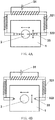
- FIG. 4A is a schematic diagram of a magnetic-field applying device according to a further example of the present invention (extended position)
- FIG. 4B is a schematic view of a non-operating state of FIG. 4A (retracted position).
- the magnetic-field applying device 3 comprises a power supply 31, a magnetic-field generation device 32 and a pair of magnetic poles 33, wherein the magnetic-field generation device 32 comprises a coil 321 and a magnetic conductive soft iron core 322, the power supply 31 is connected to the coil 321, the coil 321 is wound on the magnetic conductive soft iron core 322 to generate a magnetic field, the magnetic conductive soft iron core 322 is of a semi-closed or quasi-closed frame structure, the magnetic poles 33 are respectively arranged at the two ends of the semi-closed frame structure, and the magnetic poles 33 and the magnetic conductive soft iron core 322 together form a closed loop circuit so that magnetic field lines are in a closed state.
- the magnetic field is generated by a Helmholtz coil 321 on the magnetic conductive soft iron core 322, and led into the vacuum chamber 1 via the magnetic conductive soft iron core 322.
- a sample stage 2 is arranged inside the vacuum chamber 1 of the nano-patterning system, the magnetic poles 33 are oppositely arranged inside the vacuum chamber 1 relative to the sample stage 2, the coil 321 and the magnetic conductive soft iron core 322 are arranged outside the vacuum chamber 1, the magnetic conductive soft iron core 322 leads the magnetic field generated by the coil 321 into the vacuum chamber 1, and the magnetic poles 33 are used for locating a sample 4 on the sample stage 2 and applying a local magnetic field.
- the magnetic poles 33 are of a telescopic structure, and said magnetic poles 33 of a telescopic structure, oppositely arranged relative to the sample stage 2, each have an extended position and a retracted position.
- each of the magnetic poles 33 is connected to an end of the magnetic conductive soft iron core 322 via a corrugated tube 34, and said magnetic poles 33, oppositely arranged relative to the sample stage 2, each have an extended position and a retracted position.
- FIG. 7 which is a schematic diagram of magnetic poles according to an example of the present invention, the magnetic poles 33 preferably are of a probe structure which has a tip with a downward curving arc 331. Or, referring to FIG.
- the magnetic poles 33 may be of a flake structure to apply a large-scale homogeneous magnetic field, and the upper surface of each said magnetic pole 33 of a flake structure has a cambered surface 332 which is concave downward.
- All of the magnetic conductive soft iron core 322 and the magnetic poles 33 are made from a non-magnetic material with magnetic permeability, or a soft magnetic material with a very small remanence, to reduce the stray field inside the vacuum chamber 1.
- the soft magnetic material can be an NiFe alloy, a silicon steel disc, or soft magnetic ferrite.
- FIGS. 9A to 9C which are schematic diagrams of magnetic pole tips according to the present invention, the tip of the magnetic pole 33 is of a planar structure, a spherical structure, or a structure with a concave cambered surface 332.
- a magnetic field of a desired size can be generated by applying an appropriate electric current to the coil 321.
- the magnetic field is led into a SEM or EBL chamber via the magnetic conductive soft iron core 322 to form a closed magnetic circuit. Since the SEM or EBL chamber is vacuum, the portion of the chamber wall where the magnetic conductive soft iron core 322 penetrates through is sealed with a corrugated tube.
- the magnetic-field applying structure at the tip of the magnetic conductive soft iron core 322 inside the chamber consists of a pair of magnetic poles 33. A magnetic field generated by the coil 321 outside the chamber is led via the magnetic conductive soft iron core 322 onto the tips of the pair of magnetic poles 33, so a phase magnetic field is generated on the sample 4.
- the two magnetic poles 33 can move back and forth mechanically and are capable of adjusting the region to which a magnetic field is applied. When there is no need to apply a magnetic field, the two magnetic poles 33 respectively withdraw to the two sides of the vacuum chamber 1.
- the specific configuration of the movable magnetic pole 33 is shown in FIG. 2C . Part of the movable magnetic pole 33 is nested inside the magnetic conductive soft iron core 322 to ensure a close contact between the two, so that the leakage of magnetic lines of force can be avoided effectively.
- the coil 321 is a wound conductive wire with high electrical conductivity. The conductive wire diameter is 0. 2 to 2 mm, and the number of turns and the diameter of the coil 321 can be determined according to the desired magnetic field.
- Said soft magnetic material is a material characterized by high permeability and small remanence. Pure iron and low carbon steel, Fe-Si alloys, Fe-Al alloys, Fe-Si-Al alloys, Ni-Fe alloys, Fe-Co alloys, soft magnetic ferrite, amorphous soft magnetic alloys, and nanocrystalline soft magnetic alloys with a particle size of about 50 nm are preferred.
- an appropriate electric current is applied to the coil 321, thus generating a magnetic field of a desired size.
- the magnetic field is led into a SEM or EBL chamber via the magnetic conductive soft iron core 322 to form a closed magnetic circuit.
- the two magnetic poles 33 simultaneously withdraw to the one side of the vacuum chamber 1.
- the advantage of such configuration is that, when there is no need to apply a magnetic field, the magnetic conductive soft iron core 322 and the magnetic poles 33 still form a closed magnetic circuit, thus effectively avoiding the leakage of remanence.
- the portion of the chamber wall where the magnetic conductive soft iron core 322 or the magnetic pole 33 penetrates through is sealed with a corrugated tube, as shown in the figures.
- an appropriate electric current is applied to the coil 321, thus generating a magnetic field of a desired size.
- the magnetic field is led into a SEM or EBL chamber via the magnetic conductive soft iron core 322 to form a closed magnetic circuit.
- the magnetic poles 33 in this embodiment are of a telescopic structure. When there is no need to apply a magnetic field, the two magnetic poles 33 simultaneously withdraw to the two sides of the vacuum chamber 1. The advantage of such configuration is that, when there is no need to apply a magnetic field, the two magnetic poles 33 retract, thus effectively saving the space inside the vacuum chamber 1.
- FIG. 5 is a schematic diagram of a magnetic-field applying device according to a further example of the present invention (extended position)
- FIG. 6A is a schematic diagram of a magnetic-field applying device according to a further example of the present invention (extended position)
- FIG. 6B is a schematic view of a non-operating state of FIG.
- the magnetic-field applying device 3 further comprises an electric-field applying device 35 which includes an electric-field applying power supply 351 and insulators 352, wherein each said insulator 352 is arranged between the magnetic conductive soft iron core 322 and the magnetic pole 33, and the electric-field applying power supply 351 is connected to both of the magnetic poles 33, so as to locate the sample and apply a local electric field.
- the electric-field applying power supply 351 supplies a DC or AC voltage so as to apply a DC or AC electric field. Even for flexible, thin insulators 352, a magnetic field in a valid closed state still can be formed.
- the magnetic-field applying device 3 can apply an electric field at the same time.
- the magnetic conductive soft iron core 322 is made of a non-magnetic metal material with high permeability, thus it is able to apply a magnetic field.
- the magnetic conductive soft iron core 322 which is in a non-magnetic metallic state, is also able to apply an electric field.
- the magnetic conductive soft iron core 322 made of a non-magnetic metal material with high permeability has almost zero remanence, thus minimizing the impact on the original function of SEM or EBL.
- the electric-field applying device 35 is added in this embodiment, wherein the insulators 352 will not affect the closed state of the magnetic circuit.
- An appropriate electric current is applied to the Helmholtz coil 321, thus generating a magnetic field of a desired size.
- the magnetic field is led into a SEM or EBL chamber via the magnetic conductive soft iron core 322 to form a closed magnetic circuit. Since the SEM or EBL chamber is vacuum, the portion of the chamber wall where the magnetic conductive soft iron core 322 penetrates through is sealed with a corrugated tube.
- a magnetic field generated by the coil 321 outside the chamber is led via the magnetic conductive soft iron core 322 onto the tips of the pair of magnetic poles 33, and applied to a local region.
- the two magnetic poles 33 at the top can also be used to apply an electric field.
- the two magnetic poles 33 which are respectively connected to the positive and negative electrodes of the electric-field applying power supply 351, form magnetic lines of force at the tips of the magnetic poles 33 and apply them to the local region.
- the two magnetic poles 33 can move back and forth mechanically and are capable of adjusting the region to which an electric field is applied.
- the magnetic poles 33 are of a telescopic structure, so that they are able to apply a local magnetic field and a local electric field, as shown in FIGS. 6A and 6B .
- the two magnetic poles 33 simultaneously withdraw to the two sides of the chamber.
- the advantage of such configuration is that, when there is no need to apply an electric field, the two magnetic poles 33 retract, thus effectively saving the space inside the chamber.
- the magnetic poles 33 that generate a magnetic field may be of a non-probe or probe structure.
- the magnetic poles 33 of a flake structure as shown in FIG. 8 can apply a large-scale homogeneous magnetic field.
- What is illustrated in FIG. 7 is a probe structure, wherein the probe may have a tip of a small size so that it is able to apply a local magnetic field to the sample 4.
- the two magnetic poles 33 can move back and forth mechanically and are capable of adjusting the region to which a magnetic field is applied. Since the SEM or EBL chamber is vacuum, the portion of the chamber wall where the magnetic conductive soft iron core 322 or the magnetic pole 33 penetrates through is sealed with a corrugated tube.
- the tip of the magnetic pole 33 for applying a magnetic field may be of a planar structure, a spherical structure, or a structure with a concave cambered surface, as shown in the figures.
- Different structures provide different distributions of stray magnetic field around the tip. After calculation, it is clear that the stray magnetic field generated at the tip in FIG. 9C is the smallest.
- the tip structure shown in FIG. 9C may be adopted. Also, calculations show that the magnetic field generated by the structure shown in FIG. 9A has the largest homogeneous region. When there is a need to measure a large homogeneous region, the tip structure shown in FIG. 9A may be adopted.
- the magnetic-field applying device is able to introduce not only a large-scale magnetic/electric field but also a large-scale or local magnetic/electric field, and it can be widely used for applying a magnetic/electric field in SEM or EBL and other apparatus. Therefore, it can be widely used not only in the fields of the measurement and study of semiconductor, microelectronic, magneto-electronic and spinning electronics materials and the devices thereof, but also in the batch testing and quality control of the related electronic products in the information industry.
- the present invention can be used for introducing a large-scale or local magnetic/electric field. It can reduce the space that a magnetic-field applying device occupies inside a SEM or EBL chamber, thereby reducing the complexity of the mechanical structure inside the chamber; it can confine the magnetic field to a local region, thereby minimizing the impact of the magnetic/electric field on the original system; it is advantageous to locate the region to be measured; and it can be used to study the local properties of the sample to be measured.
- the present invention Compared with the magnetic-field applying devices employed in the SEM or EBL systems of the prior art, the present invention allows a magnetic field, which has a minimal impact on the function of SEM or EBL, to be applied more effectively and accurately, thus it can be used to quickly and efficiently apply magnetic fields in the tests and studies of nano materials and devices as well as the array samples thereof. Therefore, the present invention can be widely used in many fields and meet the extensive market demands.
Landscapes
- Physics & Mathematics (AREA)
- Electromagnetism (AREA)
- Engineering & Computer Science (AREA)
- Power Engineering (AREA)
- General Physics & Mathematics (AREA)
- Condensed Matter Physics & Semiconductors (AREA)
- Chemical & Material Sciences (AREA)
- Analytical Chemistry (AREA)
- Manufacturing & Machinery (AREA)
- Investigating Or Analyzing Materials By The Use Of Magnetic Means (AREA)
- Analysing Materials By The Use Of Radiation (AREA)
- Testing Or Measuring Of Semiconductors Or The Like (AREA)
- Sampling And Sample Adjustment (AREA)
Description
- The present invention relates to a nano-patterning and magneto-electric high-frequency characteristic measurement system, and particularly to a micro/nano-patterning system for measuring and studying the magneto-electric response characteristics of a micro/nano-patterning device as well as a magnetic-field applying device thereof.
- Since Giant Magnetoresistance (GMR) Effect and Tunneling Magnetoresistance (TMR) Effect were discovered in 1988, with the progress of the preparation of nanometer thin film materials and the micro/nano-processing technology, spinning electronics as an emerging discipline has developed rapidly and has greatly boosted the development of information science. Currently, nano-magnetic materials and devices have been widely used in many fields, including, for example, the fields of electronics, magnetics, chemistry and biology, etc. The study of nano-magnetic materials and devices has become one of the core issues of condensed matter physics and modem information technology as well as industrial production. This also means that the study of nano-magnetic materials and devices has become a complete process of comprehensive measurement and analysis, comprising nanometer microstructure imaging and nano-patterning and involving magnetic or electric fields.
- At present, Electron Beam Lithography (EBL) System is one of the important equipment for integration of the preparation and observation of nanostructures. It comprises a scanning electron microscopy (SEM) imaging function and an electron beam pattern generator, i.e. it writes nano-patterns directly on a resist layer using a focused electron beam. As the electron beam is characterized by a small beam spot and high energy, nanostructures with a line width of 5 to 10 nm can be produced by using an EBL system. This is the ideal method for making nano materials and devices. Currently, the world record of the production of nanostructures with a minimum line width of less than 5 nm was set by Raith GmbH (Germany) and has been held by it so far. Although some EBL systems have been integrated with probe arms having a function of measuring electrical signals, yet the existing EBL systems are unable to make the direct observation of nano materials and devices compatible with the manipulation and measurement of in-situ electrical/magnetic signals. This bottleneck problem is caused mainly because that the electrons used for exposure and imaging in an EBL system will deflect under the action of an external magnetic or electric field applied for the in-situ measurement of a sample, which will seriously interfere with and influence the focusing and scanning of an electron beam. To solve the above problem, we have proposed the introduction of a magnetic field into an EBL system in the Chinese utility model patent No.
201120265595.5 - US patent
US 20040173755A1 recorded an electron-beam focusing apparatus for controlling a path of electron beams emitted from an electron-beam emitter in an electron-beam projection lithography (EPL) system includes top and bottom magnets for creating a magnetic field within a vacuum chamber, the top and bottom magnets disposed above and below the vacuum chamber into which a wafer is loaded, respectively; upper and lower pole pieces magnetically contacting the top and bottom magnets, respec-tively, the upper and lower pole pieces penetrating a top wall and a bottom wall of the vacuum chamber, respectively; and upper and lower projections having a circular shape, extend-ing outwardly from facing surfaces of the upper and lower pole pieces, respectively. - US patent
US 5900728 recorded an alternating current (AC) magnetic force microscopy (MFM) system incorporates an improved probe with an integrated coil on the free end of the system's cantilever. The probe has a pair of magnetic poles that form part of a magnetic yoke and a patterned electrically conductive coil wound through the yoke. The probe includes a probe tip that has a magnetic surface layer that is magnetically coupled to one of the poles and extends from it. When alternating current from the AC-MFM system is passed through the probe coil the magnetization direction of the probe tipcorrespondingly alternates. The interaction of these alternat-ing magnetic fields from the probe tip with the magnetic fields emanating from the sample whose magnetic fields are to be measured causes the cantilever to deflect between two extreme positions. The probe can be formed from a portion of a disk drive air-bearing slider with a patterned thin film inductive write head on its trailing end by growing the probe tip from the slider's air-bearing surface so as to be in contact with the gap and one of the poles of the write head. The probe can also be part of an integrated single-piece structure that includes the cantilever, probe body and probe tip which are formed using conventional thin film deposition and lithographic processes. - The technical problem to be solved by the present invention is to provide a nano-patterning system, as defined in claim 12, and a magnetic-field applying device, as defined in
claim 1, which are able to locate and introduce a magnetic field in a local region on the basis of an imaging function, such as a SEM imaging or EBL patterning function. - To this end, the present invention provides a magnetic-field applying device of a nano-patterning system, comprising a power supply, a magnetic-field generation device and a pair of movable magnetic poles, wherein the magnetic-field generation device comprises a coil and a magnetic conductive soft iron core, the power supply is connected to the coil, the coil is wound on the magnetic conductive soft iron core to generate a magnetic field, the magnetic conductive soft iron core is of a semi-closed frame structure, the magnetic poles are respectively arranged at the two ends of the semi-closed frame structure, a sample stage is arranged inside a vacuum chamber of the nano-patterning system, the magnetic poles are oppositely arranged inside the vacuum chamber relative to the sample stage, the coil and the magnetic conductive soft iron core are arranged outside the vacuum chamber, the magnetic conductive soft iron core leads the magnetic field generated by the coil into the vacuum chamber, and the magnetic poles are used for locating a sample on the sample stage and applying a local magnetic field.
- In the magnetic-field applying device, the magnetic poles are of a telescopic structure, and said magnetic poles of a telescopic structure, oppositely arranged relative to the sample stage, each have an extended position and a retracted position.
- In the magnetic-field applying device, each of the magnetic poles is connected to an end of the magnetic conductive soft iron core via a corrugated tube, and said magnetic poles, oppositely arranged relative to the sample stage, each have an extended position and a retracted position.
- In the magnetic-field applying device, the magnetic poles are of a probe structure which has a tip with a downward curving arc.
- In the magnetic-field applying device, the magnetic poles are of a flake structure to apply a large-scale homogeneous magnetic field, and the upper surface of each said magnetic pole of a flake structure has a cambered surface which is concave downward.
- In the magnetic-field applying device, the magnetic-field applying device further comprises an electric-field applying device which includes an electric-field applying power supply and insulators, each said insulator is arranged between the magnetic conductive soft iron core and the magnetic pole, and the electric-field applying power supply is connected to both of the magnetic poles, so as to locate the sample and apply a local electric field.
- In the magnetic-field applying device, the electric-field applying power supply supplies a DC or AC voltage so as to apply a DC or AC electric field.
- In the magnetic-field applying device, all of the magnetic conductive soft iron core and the magnetic poles are made from a non-magnetic material with magnetic permeability to reduce the stray field inside the vacuum chamber.
- In the magnetic-field applying device, the tip of the magnetic pole is of a planar structure, a spherical structure, or a structure with a concave cambered surface.
- To achieve the above object more efficiently, the present invention further provides a nano-patterning system comprising a vacuum chamber, a sample stage and a magnetic-field applying device, the sample stage being arranged inside the vacuum chamber, and the magnetic-field applying device being arranged relative to the sample stage, wherein the magnetic-field applying device is as defined above.
- Hereinafter, the unity model is described in detail with reference to the accompanying drawings and embodiments, which, however, are not used to limit the unity model.
-
-
FIG. 1 is a structure diagram of a nano-patterning system according to the present invention; -
FIG. 2A is a schematic diagram of a magnetic-field applying device according to an example of the present invention (extended position); -
FIG. 2B is a schematic view of a non-operating state ofFIG. 2A (retracted position); -
FIG. 2C is an installation diagram of magnetic poles according to an example of the present invention; -
FIG. 3A is a schematic diagram of a magnetic-field applying device according to another example of the present invention (extended position); -
FIG. 3B is a schematic view of a non-operating state ofFIG. 3A (retracted position); -
FIG. 4A is a schematic diagram of a magnetic-field applying device according to a further example of the present invention (extended position); -
FIG. 4B is a schematic view of a non-operating state ofFIG. 4A (retracted position); -
FIG. 5 is a schematic diagram of a magnetic-field applying device according to a further example of the present invention (extended position); -
FIG. 6A is a schematic diagram of a magnetic-field applying device according to a further example of the present invention (extended position); -
FIG. 6B is a schematic view of a non-operating state ofFIG. 6A (retracted position); -
FIG. 7 is a schematic diagram of magnetic poles according to an example of the present invention; -
FIG. 8 is a schematic diagram of magnetic poles according to another example of the present invention; and -
FIGS. 9A to 9C are schematic diagrams of magnetic pole tips according to the present invention. - The following are the relevant drawing reference signs:
- 1
- Vacuum chamber
- 2
- Sample stage
- 3
- Magnetic-field applying device
31 Power supply
32 Magnetic-field generation device
321 Coil
322 Magnetic conductive soft iron core
33 Magnetic pole
331 Arc
332 Cambered surface
34 Corrugated tube
35 Electric-field generation device
351 Electric-field applying power supply
352 Insulator - 4
- Sample
- The structural principle and working principle of the present invention are specifically described hereinafter with reference to the accompanying drawings:
- Referring to
FIG. 1 , which is a structure diagram of a nano-patterning system according to the present invention, the nano-patterning system according to the present invention comprises avacuum chamber 1, asample stage 2 and a magnetic-field applying device 3, wherein thesample stage 2 is arranged inside thevacuum chamber 1, and the magnetic-field applying device 3 is arranged relative to thesample stage 2. Since the structures and functions of the other parts of the nano-patterning system as well as the positional relationship, connection relationship and other relationships among them belong to existing technologies which are relatively mature, the details are not repeated here. Next, only the magnetic-field applying device 3 according to the present invention will be described in detail. - Referring to
FIGS. 2A to 4B , whereinFIG. 2A is a schematic diagram of a magnetic-field applying device according to an example of the present invention (extended position),FIG. 2B is a schematic view of a non-operating state ofFIG. 2A (retracted position),FIG. 3A is a schematic diagram of a magnetic-field applying device according to another example of the present invention (extended position),FIG. 3B is a schematic view of a non-operating state ofFIG. 3A (retracted position),FIG. 4A is a schematic diagram of a magnetic-field applying device according to a further example of the present invention (extended position), andFIG. 4B is a schematic view of a non-operating state ofFIG. 4A (retracted position). The magnetic-field applying device 3 according to the present invention comprises apower supply 31, a magnetic-field generation device 32 and a pair ofmagnetic poles 33, wherein the magnetic-field generation device 32 comprises acoil 321 and a magnetic conductivesoft iron core 322, thepower supply 31 is connected to thecoil 321, thecoil 321 is wound on the magnetic conductivesoft iron core 322 to generate a magnetic field, the magnetic conductivesoft iron core 322 is of a semi-closed or quasi-closed frame structure, themagnetic poles 33 are respectively arranged at the two ends of the semi-closed frame structure, and themagnetic poles 33 and the magnetic conductivesoft iron core 322 together form a closed loop circuit so that magnetic field lines are in a closed state. The magnetic field is generated by aHelmholtz coil 321 on the magnetic conductivesoft iron core 322, and led into thevacuum chamber 1 via the magnetic conductivesoft iron core 322. Asample stage 2 is arranged inside thevacuum chamber 1 of the nano-patterning system, themagnetic poles 33 are oppositely arranged inside thevacuum chamber 1 relative to thesample stage 2, thecoil 321 and the magnetic conductivesoft iron core 322 are arranged outside thevacuum chamber 1, the magnetic conductivesoft iron core 322 leads the magnetic field generated by thecoil 321 into thevacuum chamber 1, and themagnetic poles 33 are used for locating asample 4 on thesample stage 2 and applying a local magnetic field. - In this embodiment, the
magnetic poles 33 are of a telescopic structure, and saidmagnetic poles 33 of a telescopic structure, oppositely arranged relative to thesample stage 2, each have an extended position and a retracted position. In addition, each of themagnetic poles 33 is connected to an end of the magnetic conductivesoft iron core 322 via acorrugated tube 34, and saidmagnetic poles 33, oppositely arranged relative to thesample stage 2, each have an extended position and a retracted position. Referring toFIG. 7 , which is a schematic diagram of magnetic poles according to an example of the present invention, themagnetic poles 33 preferably are of a probe structure which has a tip with a downward curvingarc 331. Or, referring toFIG. 8 , which is a schematic diagram of magnetic poles according to another example of the present invention, themagnetic poles 33 may be of a flake structure to apply a large-scale homogeneous magnetic field, and the upper surface of each saidmagnetic pole 33 of a flake structure has acambered surface 332 which is concave downward. All of the magnetic conductivesoft iron core 322 and themagnetic poles 33 are made from a non-magnetic material with magnetic permeability, or a soft magnetic material with a very small remanence, to reduce the stray field inside thevacuum chamber 1. The soft magnetic material can be an NiFe alloy, a silicon steel disc, or soft magnetic ferrite.
Referring toFIGS. 9A to 9C , which are schematic diagrams of magnetic pole tips according to the present invention, the tip of themagnetic pole 33 is of a planar structure, a spherical structure, or a structure with a concavecambered surface 332. - Referring to
FIGS. 2A to 2C , a magnetic field of a desired size can be generated by applying an appropriate electric current to thecoil 321. The magnetic field is led into a SEM or EBL chamber via the magnetic conductivesoft iron core 322 to form a closed magnetic circuit. Since the SEM or EBL chamber is vacuum, the portion of the chamber wall where the magnetic conductivesoft iron core 322 penetrates through is sealed with a corrugated tube. The magnetic-field applying structure at the tip of the magnetic conductivesoft iron core 322 inside the chamber consists of a pair ofmagnetic poles 33. A magnetic field generated by thecoil 321 outside the chamber is led via the magnetic conductivesoft iron core 322 onto the tips of the pair ofmagnetic poles 33, so a phase magnetic field is generated on thesample 4. The twomagnetic poles 33 can move back and forth mechanically and are capable of adjusting the region to which a magnetic field is applied. When there is no need to apply a magnetic field, the twomagnetic poles 33 respectively withdraw to the two sides of thevacuum chamber 1. The specific configuration of the movablemagnetic pole 33 is shown inFIG. 2C . Part of the movablemagnetic pole 33 is nested inside the magnetic conductivesoft iron core 322 to ensure a close contact between the two, so that the leakage of magnetic lines of force can be avoided effectively. Thecoil 321 is a wound conductive wire with high electrical conductivity. The conductive wire diameter is 0. 2 to 2 mm, and the number of turns and the diameter of thecoil 321 can be determined according to the desired magnetic field. Periphery of thecoil 321 can be cooled by wrapping it with a circulating water jacket. Said soft magnetic material is a material characterized by high permeability and small remanence. Pure iron and low carbon steel, Fe-Si alloys, Fe-Al alloys, Fe-Si-Al alloys, Ni-Fe alloys, Fe-Co alloys, soft magnetic ferrite, amorphous soft magnetic alloys, and nanocrystalline soft magnetic alloys with a particle size of about 50 nm are preferred. - Referring to
FIGS. 3A and 3B , an appropriate electric current is applied to thecoil 321, thus generating a magnetic field of a desired size. The magnetic field is led into a SEM or EBL chamber via the magnetic conductivesoft iron core 322 to form a closed magnetic circuit. When there is no need to apply a magnetic field, the twomagnetic poles 33 simultaneously withdraw to the one side of thevacuum chamber 1. The advantage of such configuration is that, when there is no need to apply a magnetic field, the magnetic conductivesoft iron core 322 and themagnetic poles 33 still form a closed magnetic circuit, thus effectively avoiding the leakage of remanence. Similarly, the portion of the chamber wall where the magnetic conductivesoft iron core 322 or themagnetic pole 33 penetrates through is sealed with a corrugated tube, as shown in the figures. - Referring to
FIGS. 4A and 4B , an appropriate electric current is applied to thecoil 321, thus generating a magnetic field of a desired size. The magnetic field is led into a SEM or EBL chamber via the magnetic conductivesoft iron core 322 to form a closed magnetic circuit. Themagnetic poles 33 in this embodiment are of a telescopic structure. When there is no need to apply a magnetic field, the twomagnetic poles 33 simultaneously withdraw to the two sides of thevacuum chamber 1. The advantage of such configuration is that, when there is no need to apply a magnetic field, the twomagnetic poles 33 retract, thus effectively saving the space inside thevacuum chamber 1. - Referring to
FIGS. 5 to 6B , whereinFIG. 5 is a schematic diagram of a magnetic-field applying device according to a further example of the present invention (extended position),FIG. 6A is a schematic diagram of a magnetic-field applying device according to a further example of the present invention (extended position), andFIG. 6B is a schematic view of a non-operating state ofFIG. 6A (retracted position) In this embodiment, the magnetic-field applying device 3 further comprises an electric-field applying device 35 which includes an electric-field applyingpower supply 351 andinsulators 352, wherein each saidinsulator 352 is arranged between the magnetic conductivesoft iron core 322 and themagnetic pole 33, and the electric-field applyingpower supply 351 is connected to both of themagnetic poles 33, so as to locate the sample and apply a local electric field. The electric-field applyingpower supply 351 supplies a DC or AC voltage so as to apply a DC or AC electric field. Even for flexible,thin insulators 352, a magnetic field in a valid closed state still can be formed. Meanwhile, owing to theinsulators 352 disposed therein, the magnetic-field applying device 3 can apply an electric field at the same time. The magnetic conductivesoft iron core 322 is made of a non-magnetic metal material with high permeability, thus it is able to apply a magnetic field. In the case where no magnetic field is applied, the magnetic conductivesoft iron core 322, which is in a non-magnetic metallic state, is also able to apply an electric field. In addition, when no magnetic field is applied, the magnetic conductivesoft iron core 322 made of a non-magnetic metal material with high permeability has almost zero remanence, thus minimizing the impact on the original function of SEM or EBL. - Referring to
FIG. 5 , the electric-field applying device 35 is added in this embodiment, wherein theinsulators 352 will not affect the closed state of the magnetic circuit. An appropriate electric current is applied to theHelmholtz coil 321, thus generating a magnetic field of a desired size. The magnetic field is led into a SEM or EBL chamber via the magnetic conductivesoft iron core 322 to form a closed magnetic circuit. Since the SEM or EBL chamber is vacuum, the portion of the chamber wall where the magnetic conductivesoft iron core 322 penetrates through is sealed with a corrugated tube. A magnetic field generated by thecoil 321 outside the chamber is led via the magnetic conductivesoft iron core 322 onto the tips of the pair ofmagnetic poles 33, and applied to a local region. But beyond that, due to the presence of theinsulators 352, the twomagnetic poles 33 at the top can also be used to apply an electric field. The twomagnetic poles 33, which are respectively connected to the positive and negative electrodes of the electric-field applyingpower supply 351, form magnetic lines of force at the tips of themagnetic poles 33 and apply them to the local region. The twomagnetic poles 33 can move back and forth mechanically and are capable of adjusting the region to which an electric field is applied. Themagnetic poles 33 are of a telescopic structure, so that they are able to apply a local magnetic field and a local electric field, as shown inFIGS. 6A and6B . When there is no need to apply an electric field, the twomagnetic poles 33 simultaneously withdraw to the two sides of the chamber. The advantage of such configuration is that, when there is no need to apply an electric field, the twomagnetic poles 33 retract, thus effectively saving the space inside the chamber. - Referring to
FIGS. 7 and 8 , themagnetic poles 33 that generate a magnetic field may be of a non-probe or probe structure. Themagnetic poles 33 of a flake structure as shown inFIG. 8 can apply a large-scale homogeneous magnetic field. What is illustrated inFIG. 7 is a probe structure, wherein the probe may have a tip of a small size so that it is able to apply a local magnetic field to thesample 4. The twomagnetic poles 33 can move back and forth mechanically and are capable of adjusting the region to which a magnetic field is applied. Since the SEM or EBL chamber is vacuum, the portion of the chamber wall where the magnetic conductivesoft iron core 322 or themagnetic pole 33 penetrates through is sealed with a corrugated tube. - Referring to
FIGS. 9A to 9C , the tip of themagnetic pole 33 for applying a magnetic field may be of a planar structure, a spherical structure, or a structure with a concave cambered surface, as shown in the figures. Different structures provide different distributions of stray magnetic field around the tip. After calculation, it is clear that the stray magnetic field generated at the tip inFIG. 9C is the smallest. To apply a magnetic field required to have a reduced stray magnetic field, the tip structure shown inFIG. 9C may be adopted. Also, calculations show that the magnetic field generated by the structure shown inFIG. 9A has the largest homogeneous region. When there is a need to measure a large homogeneous region, the tip structure shown inFIG. 9A may be adopted. - The magnetic-field applying device according to the present invention is able to introduce not only a large-scale magnetic/electric field but also a large-scale or local magnetic/electric field, and it can be widely used for applying a magnetic/electric field in SEM or EBL and other apparatus. Therefore, it can be widely used not only in the fields of the measurement and study of semiconductor, microelectronic, magneto-electronic and spinning electronics materials and the devices thereof, but also in the batch testing and quality control of the related electronic products in the information industry.
- Of course, the present invention may have a variety of other embodiments. Those skilled in the art can make all kinds of corresponding changes and modifications according to the present invention without departing from the spirit and essence of the present invention. It is intended that all these changes and modifications be covered by the appended claims of the present invention.
- The present invention can be used for introducing a large-scale or local magnetic/electric field. It can reduce the space that a magnetic-field applying device occupies inside a SEM or EBL chamber, thereby reducing the complexity of the mechanical structure inside the chamber; it can confine the magnetic field to a local region, thereby minimizing the impact of the magnetic/electric field on the original system; it is advantageous to locate the region to be measured; and it can be used to study the local properties of the sample to be measured. Compared with the magnetic-field applying devices employed in the SEM or EBL systems of the prior art, the present invention allows a magnetic field, which has a minimal impact on the function of SEM or EBL, to be applied more effectively and accurately, thus it can be used to quickly and efficiently apply magnetic fields in the tests and studies of nano materials and devices as well as the array samples thereof. Therefore, the present invention can be widely used in many fields and meet the extensive market demands.
Claims (15)
- A magnetic-field applying device of a nano-patterning system, comprising a power supply (31), a magnetic-field generation device (32) and a pair of movable magnetic poles (33), the magnetic-field generation device (32) comprises a coil (321) and a magnetic conductive soft iron core (322), the power supply (31) is connected to the coil (321), the coil (321) is wound on the magnetic conductive soft iron core (322) to generate a magnetic field, characterized that the magnetic conductive soft iron core (322) is of a semi-closed frame structure, the movable magnetic poles (33) are respectively arranged at the two ends of the semi-closed frame structure, a sample stage (2) is arranged inside a vacuum chamber (1) of the nano-patterning system, the movable magnetic poles (33) are oppositely arranged inside the vacuum chamber (1) relative to the sample stage (2), the coil (321) and the magnetic conductive soft iron core (322) are arranged outside the vacuum chamber (1), the magnetic conductive soft iron core (322) leads the magnetic field generated by the coil (321) into the vacuum chamber (1), and the movable magnetic poles (33) are used for locating a sample (4) on the sample stage (2) and applying a local magnetic field.
- The magnetic-field applying device according to claim 1, wherein the movable magnetic poles (33) are of a telescopic structure, said movable magnetic poles (33) of a telescopic structure, oppositely arranged relative to the sample stage (2), each having an extended position and a retracted position.
- The magnetic-field applying device according to claim 1, wherein each of the movable magnetic poles (33) is connected to an end of the magnetic conductive soft iron core (322) via a corrugated tube (34), said movable magnetic poles (33), oppositely arranged relative to the sample stage (2), each having an extended position and a retracted position.
- The magnetic-field applying device according to claim 1, wherein the movable magnetic poles (33) are of a probe structure which has a tip with a downward curving arc (331).
- The magnetic-field applying device according to claim 1, wherein the movable magnetic poles (33) are of a flake structure to apply a large-scale homogeneous magnetic field, the upper surface of each said magnetic pole (33) of a flake structure having a cambered surface (332) which is concave downward.
- The magnetic-field applying device according to either one of claims 1, 2, 3 and 5, wherein the magnetic-field applying device (3) further comprises an electric-field applying device which includes an electric-field applying power supply (351) and insulators (352), each said insulator (352) being arranged between the magnetic conductive soft iron core (322) and the magnetic pole (33), and the electric-field applying power supply (351) being connected to both of the movable magnetic poles (33), so as to locate the sample (4) and apply a local electric field.
- The magnetic-field applying device according to claim 6, wherein the electric-field applying power supply (351) supplies a DC or AC voltage so as to apply a DC or AC electric field.
- The magnetic-field applying device according to claim 6, wherein all of the magnetic conductive soft iron core (322) and the movable magnetic poles (33) are made from a non-magnetic material with magnetic permeability to reduce the stray field inside the vacuum chamber (1).
- The magnetic-field applying device according to claim 7, wherein all of the magnetic conductive soft iron core (322) and the movable magnetic poles (33) are made from a non-magnetic material with magnetic permeability to reduce the stray field inside the vacuum chamber (1).
- The magnetic-field applying device according to claim 6, wherein the tip of the magnetic pole (33) is of a planar structure, a spherical structure, or a structure with a concave cambered surface (332).
- The magnetic-field applying device according to claim 7, wherein the tip of the magnetic pole (33) is of a planar structure, a spherical structure, or a structure with a concave cambered surface (332).
- A nano-patterning system comprising a vacuum chamber (1), a sample stage (2) and a magnetic-field applying device (3), the sample stage (2) being arranged inside the vacuum chamber (1), and the magnetic-field applying device (3) being arranged relative to the sample stage (2), wherein the magnetic-field applying device (3)is as defined in claim 1.
- A nano-patterning system comprising a vacuum chamber (1), a sample stage (2) and a magnetic-field applying device (3), the sample stage (2) being arranged inside the vacuum chamber (1), and the magnetic-field applying device (3) being arranged relative to the sample stage (2), wherein the magnetic-field applying device (3) is as defined in claim 6.
- A nano-patterning system comprising a vacuum chamber (1), a sample stage (2) and a magnetic-field applying device (3), the sample stage (2) being arranged inside the vacuum chamber (1), and the magnetic-field applying device (3) being arranged relative to the sample stage (2), wherein the magnetic-field applying device (3) is as defined in claim 9.
- A nano-patterning system comprising a vacuum chamber (1), a sample stage (2) and a magnetic-field applying device (3), the sample stage (2) being arranged inside the vacuum chamber (1), and the magnetic-field applying device (3) being arranged relative to the sample stage (2), wherein the magnetic-field applying device (3) is as defined in claim 11.
Applications Claiming Priority (2)
| Application Number | Priority Date | Filing Date | Title |
|---|---|---|---|
| CN201210096470.3A CN103365101B (en) | 2012-04-01 | 2012-04-01 | Nano-imaging system and magnetic field applying device thereof |
| PCT/CN2012/078751 WO2013149444A1 (en) | 2012-04-01 | 2012-07-17 | Nano-patterned system and magnetic-field applying device thereof |
Publications (3)
| Publication Number | Publication Date |
|---|---|
| EP2835688A1 EP2835688A1 (en) | 2015-02-11 |
| EP2835688A4 EP2835688A4 (en) | 2015-12-30 |
| EP2835688B1 true EP2835688B1 (en) | 2017-05-17 |
Family
ID=49299954
Family Applications (1)
| Application Number | Title | Priority Date | Filing Date |
|---|---|---|---|
| EP12873678.2A Active EP2835688B1 (en) | 2012-04-01 | 2012-07-17 | Nano-patterned system and magnetic-field applying device thereof |
Country Status (4)
| Country | Link |
|---|---|
| US (2) | US9484138B2 (en) |
| EP (1) | EP2835688B1 (en) |
| CN (1) | CN103365101B (en) |
| WO (1) | WO2013149444A1 (en) |
Families Citing this family (9)
| Publication number | Priority date | Publication date | Assignee | Title |
|---|---|---|---|---|
| FR3046695B1 (en) * | 2016-01-11 | 2018-05-11 | Centre National De La Recherche Scientifique | MAGNETIC FIELD GENERATOR |
| TWI607227B (en) * | 2016-11-03 | 2017-12-01 | 國立清華大學 | Measuring apparatus for electromagnetic property of material and measuring method thereof |
| CN108023507A (en) * | 2018-01-20 | 2018-05-11 | 营口万意达智能装备科技有限公司 | A kind of accurate start stop apparatus of slippage magnetic suspension |
| KR102079024B1 (en) * | 2018-10-25 | 2020-04-07 | 한국기초과학지원연구원 | Magnetic Field Station, Insert Assembly, Mount assembly and 2-Axis Magnetic Generating Equipment Including Thereof |
| CN110690024B (en) * | 2019-10-12 | 2020-10-02 | 燕山大学 | Magnetic field generating device and manufacturing method thereof |
| CN112038039B (en) * | 2020-05-27 | 2021-08-24 | 中国科学院宁波材料技术与工程研究所 | A magnetic field generating device and a transmission electron microscope sample rod capable of applying a magnetic field |
| CN114660515B (en) * | 2020-12-22 | 2025-07-22 | 财团法人工业技术研究院 | Magnetic field structure |
| CN113555204A (en) * | 2021-07-21 | 2021-10-26 | 昆山联滔电子有限公司 | Wireless charging coil piece and wireless charging coil assembly |
| EP4388573A1 (en) * | 2021-08-20 | 2024-06-26 | Forschungszentrum Jülich GmbH | Magnetization device for an electron microscope and method |
Family Cites Families (9)
| Publication number | Priority date | Publication date | Assignee | Title |
|---|---|---|---|---|
| US5539366A (en) * | 1994-07-27 | 1996-07-23 | General Electric Company | Magnet having contoured pole faces for magnetic field homogeneity |
| US5900728A (en) * | 1997-03-20 | 1999-05-04 | International Business Machines Corporation | Alternating current magnetic force microscopy system with probe having integrated coil |
| JP3285568B2 (en) * | 1999-05-24 | 2002-05-27 | 日本電産リード株式会社 | Board wiring inspection apparatus and wiring inspection method |
| JP2004158612A (en) | 2002-11-06 | 2004-06-03 | Nikon Corp | Magnetic field canceller and charged particle beam exposure apparatus having the same |
| KR100951729B1 (en) * | 2003-03-07 | 2010-04-07 | 삼성전자주식회사 | Electron Beam Focusing Device and Electron Beam Projection Lithography System |
| CN100340863C (en) | 2004-06-15 | 2007-10-03 | 华南师范大学 | Automatic tester for semiconductor epitaxial sheet performance and testing method thereof |
| JP4585434B2 (en) * | 2005-11-30 | 2010-11-24 | 富士通株式会社 | Probe card |
| EP1798751A1 (en) * | 2005-12-13 | 2007-06-20 | ICT Integrated Circuit Testing Gesellschaft für Halbleiterprüftechnik mbH | Protecting aperture for charged particle emitter |
| CN202533709U (en) * | 2012-04-01 | 2012-11-14 | 中国科学院物理研究所 | Nano graphical system and magnetic field applying device thereof |
-
2012
- 2012-04-01 CN CN201210096470.3A patent/CN103365101B/en active Active
- 2012-07-17 EP EP12873678.2A patent/EP2835688B1/en active Active
- 2012-07-17 WO PCT/CN2012/078751 patent/WO2013149444A1/en not_active Ceased
- 2012-07-17 US US14/389,972 patent/US9484138B2/en active Active
-
2016
- 2016-09-30 US US15/282,028 patent/US9640363B2/en active Active
Also Published As
| Publication number | Publication date |
|---|---|
| EP2835688A1 (en) | 2015-02-11 |
| US9640363B2 (en) | 2017-05-02 |
| CN103365101B (en) | 2015-04-08 |
| EP2835688A4 (en) | 2015-12-30 |
| CN103365101A (en) | 2013-10-23 |
| US20150123754A1 (en) | 2015-05-07 |
| US9484138B2 (en) | 2016-11-01 |
| US20170018395A1 (en) | 2017-01-19 |
| WO2013149444A1 (en) | 2013-10-10 |
Similar Documents
| Publication | Publication Date | Title |
|---|---|---|
| US9640363B2 (en) | Nano-patterned system and magnetic-field applying device thereof | |
| EP2738607B1 (en) | Nanopatterning and ultra-wideband electromagnetic characteristic measurement system | |
| CN202189227U (en) | Nano imaging and ultra-wide band electromagnetic property measurement system | |
| Todorovic et al. | Writing and reading of single magnetic domain per bit perpendicular patterned media | |
| EP2795656B1 (en) | Charged particle vortex wave generation | |
| US20200073257A1 (en) | Wafer alignment markers, systems, and related methods | |
| US20230089136A1 (en) | Magnetic field generation device, and transmission electron microscope sample holder capable of applying magnetic field | |
| Matteucci et al. | Flux measurements on ferromagnetic microprobes by electron holography | |
| CN202533709U (en) | Nano graphical system and magnetic field applying device thereof | |
| KR101746504B1 (en) | High magnetic cavity apparatus and rf neutron spin flipper apparatus having the same | |
| CN206740683U (en) | A kind of nano-controller original position magnetotransport measuring instrument | |
| Nurgazizov et al. | Magnetic force microscopy investigation of the magnetization reversal of permalloy particles at high temperatures | |
| JP2012008072A (en) | Measurement method of direction and density of current, display method, and measurement display device thereof | |
| JP3693165B2 (en) | Magnetic shield characteristic measuring device | |
| Luo et al. | Quantitative magnetization measurements of magnetic particles with FePt standard samples | |
| Wartelle et al. | Broadband setup for magnetic-field-induced domain wall motion in cylindrical nanowires | |
| CN204162408U (en) | A kind of nano graph preparation system and magnetic field applicator thereof | |
| Singh | Magnetic Domains and Domain Wall Oscillations in Planar and 3D Curved Membranes | |
| Rodríguez et al. | Nanoscale magnetic imaging of chemically modulated FeCo nanowires | |
| Scott | Characterisation of MFM tip stray fields using Lorentz electron tomography | |
| YUNSONG | Magnetic reversal and vortex chiralities in submicron cobalt dots | |
| Celotta et al. | Magnetic Domain Imaging of Spintronic Devices | |
| CN120019456A (en) | Magnetic components, especially quantum components | |
| Hayashi et al. | Intentionally encapsulated metal alloys within vertically aligned multi-walled carbon nanotube array via chemical vapor deposition technique | |
| He | Quantitative Phase Imaging of Magnetic Nanostructures Using Off-Axis Electron Holography |
Legal Events
| Date | Code | Title | Description |
|---|---|---|---|
| PUAI | Public reference made under article 153(3) epc to a published international application that has entered the european phase |
Free format text: ORIGINAL CODE: 0009012 |
|
| 17P | Request for examination filed |
Effective date: 20140828 |
|
| AK | Designated contracting states |
Kind code of ref document: A1 Designated state(s): AL AT BE BG CH CY CZ DE DK EE ES FI FR GB GR HR HU IE IS IT LI LT LU LV MC MK MT NL NO PL PT RO RS SE SI SK SM TR |
|
| AX | Request for extension of the european patent |
Extension state: BA ME |
|
| DAX | Request for extension of the european patent (deleted) | ||
| RA4 | Supplementary search report drawn up and despatched (corrected) |
Effective date: 20151202 |
|
| RIC1 | Information provided on ipc code assigned before grant |
Ipc: G01R 31/00 20060101ALI20151126BHEP Ipc: G03F 7/20 20060101AFI20151126BHEP Ipc: H01F 7/20 20060101ALI20151126BHEP Ipc: H01L 43/12 20060101ALI20151126BHEP Ipc: G01R 33/09 20060101ALI20151126BHEP Ipc: H01J 37/09 20060101ALI20151126BHEP Ipc: H01F 41/00 20060101ALI20151126BHEP |
|
| GRAP | Despatch of communication of intention to grant a patent |
Free format text: ORIGINAL CODE: EPIDOSNIGR1 |
|
| INTG | Intention to grant announced |
Effective date: 20161220 |
|
| GRAS | Grant fee paid |
Free format text: ORIGINAL CODE: EPIDOSNIGR3 |
|
| GRAA | (expected) grant |
Free format text: ORIGINAL CODE: 0009210 |
|
| AK | Designated contracting states |
Kind code of ref document: B1 Designated state(s): AL AT BE BG CH CY CZ DE DK EE ES FI FR GB GR HR HU IE IS IT LI LT LU LV MC MK MT NL NO PL PT RO RS SE SI SK SM TR |
|
| REG | Reference to a national code |
Ref country code: GB Ref legal event code: FG4D |
|
| REG | Reference to a national code |
Ref country code: CH Ref legal event code: EP |
|
| REG | Reference to a national code |
Ref country code: IE Ref legal event code: FG4D |
|
| REG | Reference to a national code |
Ref country code: AT Ref legal event code: REF Ref document number: 894998 Country of ref document: AT Kind code of ref document: T Effective date: 20170615 |
|
| REG | Reference to a national code |
Ref country code: DE Ref legal event code: R096 Ref document number: 602012032699 Country of ref document: DE |
|
| REG | Reference to a national code |
Ref country code: NL Ref legal event code: MP Effective date: 20170517 |
|
| REG | Reference to a national code |
Ref country code: LT Ref legal event code: MG4D |
|
| REG | Reference to a national code |
Ref country code: AT Ref legal event code: MK05 Ref document number: 894998 Country of ref document: AT Kind code of ref document: T Effective date: 20170517 |
|
| PG25 | Lapsed in a contracting state [announced via postgrant information from national office to epo] |
Ref country code: HR Free format text: LAPSE BECAUSE OF FAILURE TO SUBMIT A TRANSLATION OF THE DESCRIPTION OR TO PAY THE FEE WITHIN THE PRESCRIBED TIME-LIMIT Effective date: 20170517 Ref country code: GR Free format text: LAPSE BECAUSE OF FAILURE TO SUBMIT A TRANSLATION OF THE DESCRIPTION OR TO PAY THE FEE WITHIN THE PRESCRIBED TIME-LIMIT Effective date: 20170818 Ref country code: ES Free format text: LAPSE BECAUSE OF FAILURE TO SUBMIT A TRANSLATION OF THE DESCRIPTION OR TO PAY THE FEE WITHIN THE PRESCRIBED TIME-LIMIT Effective date: 20170517 Ref country code: LT Free format text: LAPSE BECAUSE OF FAILURE TO SUBMIT A TRANSLATION OF THE DESCRIPTION OR TO PAY THE FEE WITHIN THE PRESCRIBED TIME-LIMIT Effective date: 20170517 Ref country code: NO Free format text: LAPSE BECAUSE OF FAILURE TO SUBMIT A TRANSLATION OF THE DESCRIPTION OR TO PAY THE FEE WITHIN THE PRESCRIBED TIME-LIMIT Effective date: 20170817 Ref country code: AT Free format text: LAPSE BECAUSE OF FAILURE TO SUBMIT A TRANSLATION OF THE DESCRIPTION OR TO PAY THE FEE WITHIN THE PRESCRIBED TIME-LIMIT Effective date: 20170517 Ref country code: FI Free format text: LAPSE BECAUSE OF FAILURE TO SUBMIT A TRANSLATION OF THE DESCRIPTION OR TO PAY THE FEE WITHIN THE PRESCRIBED TIME-LIMIT Effective date: 20170517 |
|
| PG25 | Lapsed in a contracting state [announced via postgrant information from national office to epo] |
Ref country code: IS Free format text: LAPSE BECAUSE OF FAILURE TO SUBMIT A TRANSLATION OF THE DESCRIPTION OR TO PAY THE FEE WITHIN THE PRESCRIBED TIME-LIMIT Effective date: 20170917 Ref country code: BG Free format text: LAPSE BECAUSE OF FAILURE TO SUBMIT A TRANSLATION OF THE DESCRIPTION OR TO PAY THE FEE WITHIN THE PRESCRIBED TIME-LIMIT Effective date: 20170817 Ref country code: NL Free format text: LAPSE BECAUSE OF FAILURE TO SUBMIT A TRANSLATION OF THE DESCRIPTION OR TO PAY THE FEE WITHIN THE PRESCRIBED TIME-LIMIT Effective date: 20170517 Ref country code: LV Free format text: LAPSE BECAUSE OF FAILURE TO SUBMIT A TRANSLATION OF THE DESCRIPTION OR TO PAY THE FEE WITHIN THE PRESCRIBED TIME-LIMIT Effective date: 20170517 Ref country code: RS Free format text: LAPSE BECAUSE OF FAILURE TO SUBMIT A TRANSLATION OF THE DESCRIPTION OR TO PAY THE FEE WITHIN THE PRESCRIBED TIME-LIMIT Effective date: 20170517 Ref country code: PL Free format text: LAPSE BECAUSE OF FAILURE TO SUBMIT A TRANSLATION OF THE DESCRIPTION OR TO PAY THE FEE WITHIN THE PRESCRIBED TIME-LIMIT Effective date: 20170517 Ref country code: SE Free format text: LAPSE BECAUSE OF FAILURE TO SUBMIT A TRANSLATION OF THE DESCRIPTION OR TO PAY THE FEE WITHIN THE PRESCRIBED TIME-LIMIT Effective date: 20170517 |
|
| PG25 | Lapsed in a contracting state [announced via postgrant information from national office to epo] |
Ref country code: CZ Free format text: LAPSE BECAUSE OF FAILURE TO SUBMIT A TRANSLATION OF THE DESCRIPTION OR TO PAY THE FEE WITHIN THE PRESCRIBED TIME-LIMIT Effective date: 20170517 Ref country code: RO Free format text: LAPSE BECAUSE OF FAILURE TO SUBMIT A TRANSLATION OF THE DESCRIPTION OR TO PAY THE FEE WITHIN THE PRESCRIBED TIME-LIMIT Effective date: 20170517 Ref country code: DK Free format text: LAPSE BECAUSE OF FAILURE TO SUBMIT A TRANSLATION OF THE DESCRIPTION OR TO PAY THE FEE WITHIN THE PRESCRIBED TIME-LIMIT Effective date: 20170517 Ref country code: SK Free format text: LAPSE BECAUSE OF FAILURE TO SUBMIT A TRANSLATION OF THE DESCRIPTION OR TO PAY THE FEE WITHIN THE PRESCRIBED TIME-LIMIT Effective date: 20170517 Ref country code: EE Free format text: LAPSE BECAUSE OF FAILURE TO SUBMIT A TRANSLATION OF THE DESCRIPTION OR TO PAY THE FEE WITHIN THE PRESCRIBED TIME-LIMIT Effective date: 20170517 |
|
| REG | Reference to a national code |
Ref country code: DE Ref legal event code: R097 Ref document number: 602012032699 Country of ref document: DE |
|
| PG25 | Lapsed in a contracting state [announced via postgrant information from national office to epo] |
Ref country code: SM Free format text: LAPSE BECAUSE OF FAILURE TO SUBMIT A TRANSLATION OF THE DESCRIPTION OR TO PAY THE FEE WITHIN THE PRESCRIBED TIME-LIMIT Effective date: 20170517 Ref country code: IT Free format text: LAPSE BECAUSE OF FAILURE TO SUBMIT A TRANSLATION OF THE DESCRIPTION OR TO PAY THE FEE WITHIN THE PRESCRIBED TIME-LIMIT Effective date: 20170517 |
|
| REG | Reference to a national code |
Ref country code: CH Ref legal event code: PL |
|
| PLBE | No opposition filed within time limit |
Free format text: ORIGINAL CODE: 0009261 |
|
| STAA | Information on the status of an ep patent application or granted ep patent |
Free format text: STATUS: NO OPPOSITION FILED WITHIN TIME LIMIT |
|
| REG | Reference to a national code |
Ref country code: IE Ref legal event code: MM4A |
|
| 26N | No opposition filed |
Effective date: 20180220 |
|
| GBPC | Gb: european patent ceased through non-payment of renewal fee |
Effective date: 20170817 |
|
| REG | Reference to a national code |
Ref country code: FR Ref legal event code: ST Effective date: 20180330 |
|
| PG25 | Lapsed in a contracting state [announced via postgrant information from national office to epo] |
Ref country code: LI Free format text: LAPSE BECAUSE OF NON-PAYMENT OF DUE FEES Effective date: 20170731 Ref country code: CH Free format text: LAPSE BECAUSE OF NON-PAYMENT OF DUE FEES Effective date: 20170731 Ref country code: IE Free format text: LAPSE BECAUSE OF NON-PAYMENT OF DUE FEES Effective date: 20170717 |
|
| PG25 | Lapsed in a contracting state [announced via postgrant information from national office to epo] |
Ref country code: SI Free format text: LAPSE BECAUSE OF FAILURE TO SUBMIT A TRANSLATION OF THE DESCRIPTION OR TO PAY THE FEE WITHIN THE PRESCRIBED TIME-LIMIT Effective date: 20170517 Ref country code: FR Free format text: LAPSE BECAUSE OF NON-PAYMENT OF DUE FEES Effective date: 20170731 |
|
| REG | Reference to a national code |
Ref country code: BE Ref legal event code: MM Effective date: 20170731 |
|
| PG25 | Lapsed in a contracting state [announced via postgrant information from national office to epo] |
Ref country code: LU Free format text: LAPSE BECAUSE OF NON-PAYMENT OF DUE FEES Effective date: 20170717 |
|
| PG25 | Lapsed in a contracting state [announced via postgrant information from national office to epo] |
Ref country code: GB Free format text: LAPSE BECAUSE OF NON-PAYMENT OF DUE FEES Effective date: 20170817 |
|
| PG25 | Lapsed in a contracting state [announced via postgrant information from national office to epo] |
Ref country code: BE Free format text: LAPSE BECAUSE OF NON-PAYMENT OF DUE FEES Effective date: 20170731 |
|
| PG25 | Lapsed in a contracting state [announced via postgrant information from national office to epo] |
Ref country code: MT Free format text: LAPSE BECAUSE OF NON-PAYMENT OF DUE FEES Effective date: 20170717 |
|
| PG25 | Lapsed in a contracting state [announced via postgrant information from national office to epo] |
Ref country code: HU Free format text: LAPSE BECAUSE OF FAILURE TO SUBMIT A TRANSLATION OF THE DESCRIPTION OR TO PAY THE FEE WITHIN THE PRESCRIBED TIME-LIMIT; INVALID AB INITIO Effective date: 20120717 Ref country code: MC Free format text: LAPSE BECAUSE OF FAILURE TO SUBMIT A TRANSLATION OF THE DESCRIPTION OR TO PAY THE FEE WITHIN THE PRESCRIBED TIME-LIMIT Effective date: 20170517 |
|
| PG25 | Lapsed in a contracting state [announced via postgrant information from national office to epo] |
Ref country code: CY Free format text: LAPSE BECAUSE OF FAILURE TO SUBMIT A TRANSLATION OF THE DESCRIPTION OR TO PAY THE FEE WITHIN THE PRESCRIBED TIME-LIMIT Effective date: 20170517 |
|
| PG25 | Lapsed in a contracting state [announced via postgrant information from national office to epo] |
Ref country code: MK Free format text: LAPSE BECAUSE OF FAILURE TO SUBMIT A TRANSLATION OF THE DESCRIPTION OR TO PAY THE FEE WITHIN THE PRESCRIBED TIME-LIMIT Effective date: 20170517 |
|
| PG25 | Lapsed in a contracting state [announced via postgrant information from national office to epo] |
Ref country code: TR Free format text: LAPSE BECAUSE OF FAILURE TO SUBMIT A TRANSLATION OF THE DESCRIPTION OR TO PAY THE FEE WITHIN THE PRESCRIBED TIME-LIMIT Effective date: 20170517 |
|
| PG25 | Lapsed in a contracting state [announced via postgrant information from national office to epo] |
Ref country code: PT Free format text: LAPSE BECAUSE OF FAILURE TO SUBMIT A TRANSLATION OF THE DESCRIPTION OR TO PAY THE FEE WITHIN THE PRESCRIBED TIME-LIMIT Effective date: 20170517 |
|
| PG25 | Lapsed in a contracting state [announced via postgrant information from national office to epo] |
Ref country code: AL Free format text: LAPSE BECAUSE OF FAILURE TO SUBMIT A TRANSLATION OF THE DESCRIPTION OR TO PAY THE FEE WITHIN THE PRESCRIBED TIME-LIMIT Effective date: 20170517 |
|
| PGFP | Annual fee paid to national office [announced via postgrant information from national office to epo] |
Ref country code: DE Payment date: 20250708 Year of fee payment: 14 |