EP2833426A2 - Flexible display device - Google Patents
Flexible display device Download PDFInfo
- Publication number
- EP2833426A2 EP2833426A2 EP20140154706 EP14154706A EP2833426A2 EP 2833426 A2 EP2833426 A2 EP 2833426A2 EP 20140154706 EP20140154706 EP 20140154706 EP 14154706 A EP14154706 A EP 14154706A EP 2833426 A2 EP2833426 A2 EP 2833426A2
- Authority
- EP
- European Patent Office
- Prior art keywords
- flexible display
- display panel
- display device
- adhesive member
- region
- Prior art date
- Legal status (The legal status is an assumption and is not a legal conclusion. Google has not performed a legal analysis and makes no representation as to the accuracy of the status listed.)
- Granted
Links
Images



Classifications
-
- G—PHYSICS
- G09—EDUCATION; CRYPTOGRAPHY; DISPLAY; ADVERTISING; SEALS
- G09F—DISPLAYING; ADVERTISING; SIGNS; LABELS OR NAME-PLATES; SEALS
- G09F9/00—Indicating arrangements for variable information in which the information is built-up on a support by selection or combination of individual elements
- G09F9/30—Indicating arrangements for variable information in which the information is built-up on a support by selection or combination of individual elements in which the desired character or characters are formed by combining individual elements
-
- C—CHEMISTRY; METALLURGY
- C08—ORGANIC MACROMOLECULAR COMPOUNDS; THEIR PREPARATION OR CHEMICAL WORKING-UP; COMPOSITIONS BASED THEREON
- C08J—WORKING-UP; GENERAL PROCESSES OF COMPOUNDING; AFTER-TREATMENT NOT COVERED BY SUBCLASSES C08B, C08C, C08F, C08G or C08H
- C08J5/00—Manufacture of articles or shaped materials containing macromolecular substances
- C08J5/12—Bonding of a preformed macromolecular material to the same or other solid material such as metal, glass, leather, e.g. using adhesives
-
- H—ELECTRICITY
- H05—ELECTRIC TECHNIQUES NOT OTHERWISE PROVIDED FOR
- H05K—PRINTED CIRCUITS; CASINGS OR CONSTRUCTIONAL DETAILS OF ELECTRIC APPARATUS; MANUFACTURE OF ASSEMBLAGES OF ELECTRICAL COMPONENTS
- H05K7/00—Constructional details common to different types of electric apparatus
-
- H—ELECTRICITY
- H10—SEMICONDUCTOR DEVICES; ELECTRIC SOLID-STATE DEVICES NOT OTHERWISE PROVIDED FOR
- H10K—ORGANIC ELECTRIC SOLID-STATE DEVICES
- H10K50/00—Organic light-emitting devices
- H10K50/80—Constructional details
- H10K50/84—Passivation; Containers; Encapsulations
- H10K50/842—Containers
- H10K50/8426—Peripheral sealing arrangements, e.g. adhesives, sealants
-
- H—ELECTRICITY
- H10—SEMICONDUCTOR DEVICES; ELECTRIC SOLID-STATE DEVICES NOT OTHERWISE PROVIDED FOR
- H10K—ORGANIC ELECTRIC SOLID-STATE DEVICES
- H10K59/00—Integrated devices, or assemblies of multiple devices, comprising at least one organic light-emitting element covered by group H10K50/00
- H10K59/80—Constructional details
- H10K59/87—Passivation; Containers; Encapsulations
- H10K59/871—Self-supporting sealing arrangements
- H10K59/8722—Peripheral sealing arrangements, e.g. adhesives, sealants
-
- H—ELECTRICITY
- H10—SEMICONDUCTOR DEVICES; ELECTRIC SOLID-STATE DEVICES NOT OTHERWISE PROVIDED FOR
- H10K—ORGANIC ELECTRIC SOLID-STATE DEVICES
- H10K77/00—Constructional details of devices covered by this subclass and not covered by groups H10K10/80, H10K30/80, H10K50/80 or H10K59/80
- H10K77/10—Substrates, e.g. flexible substrates
- H10K77/111—Flexible substrates
-
- B—PERFORMING OPERATIONS; TRANSPORTING
- B32—LAYERED PRODUCTS
- B32B—LAYERED PRODUCTS, i.e. PRODUCTS BUILT-UP OF STRATA OF FLAT OR NON-FLAT, e.g. CELLULAR OR HONEYCOMB, FORM
- B32B2457/00—Electrical equipment
- B32B2457/20—Displays, e.g. liquid crystal displays, plasma displays
-
- B—PERFORMING OPERATIONS; TRANSPORTING
- B81—MICROSTRUCTURAL TECHNOLOGY
- B81B—MICROSTRUCTURAL DEVICES OR SYSTEMS, e.g. MICROMECHANICAL DEVICES
- B81B3/00—Devices comprising flexible or deformable elements, e.g. comprising elastic tongues or membranes
- B81B3/0097—Devices comprising flexible or deformable elements not provided for in groups B81B3/0002 - B81B3/0094
-
- C—CHEMISTRY; METALLURGY
- C09—DYES; PAINTS; POLISHES; NATURAL RESINS; ADHESIVES; COMPOSITIONS NOT OTHERWISE PROVIDED FOR; APPLICATIONS OF MATERIALS NOT OTHERWISE PROVIDED FOR
- C09K—MATERIALS FOR MISCELLANEOUS APPLICATIONS, NOT PROVIDED FOR ELSEWHERE
- C09K2323/00—Functional layers of liquid crystal optical display excluding electroactive liquid crystal layer characterised by chemical composition
- C09K2323/06—Substrate layer characterised by chemical composition
-
- G—PHYSICS
- G09—EDUCATION; CRYPTOGRAPHY; DISPLAY; ADVERTISING; SEALS
- G09F—DISPLAYING; ADVERTISING; SIGNS; LABELS OR NAME-PLATES; SEALS
- G09F9/00—Indicating arrangements for variable information in which the information is built-up on a support by selection or combination of individual elements
- G09F9/30—Indicating arrangements for variable information in which the information is built-up on a support by selection or combination of individual elements in which the desired character or characters are formed by combining individual elements
- G09F9/301—Indicating arrangements for variable information in which the information is built-up on a support by selection or combination of individual elements in which the desired character or characters are formed by combining individual elements flexible foldable or roll-able electronic displays, e.g. thin LCD, OLED
-
- H—ELECTRICITY
- H10—SEMICONDUCTOR DEVICES; ELECTRIC SOLID-STATE DEVICES NOT OTHERWISE PROVIDED FOR
- H10K—ORGANIC ELECTRIC SOLID-STATE DEVICES
- H10K2102/00—Constructional details relating to the organic devices covered by this subclass
- H10K2102/301—Details of OLEDs
- H10K2102/311—Flexible OLED
-
- H—ELECTRICITY
- H10—SEMICONDUCTOR DEVICES; ELECTRIC SOLID-STATE DEVICES NOT OTHERWISE PROVIDED FOR
- H10K—ORGANIC ELECTRIC SOLID-STATE DEVICES
- H10K50/00—Organic light-emitting devices
- H10K50/80—Constructional details
- H10K50/86—Arrangements for improving contrast, e.g. preventing reflection of ambient light
-
- H—ELECTRICITY
- H10—SEMICONDUCTOR DEVICES; ELECTRIC SOLID-STATE DEVICES NOT OTHERWISE PROVIDED FOR
- H10K—ORGANIC ELECTRIC SOLID-STATE DEVICES
- H10K59/00—Integrated devices, or assemblies of multiple devices, comprising at least one organic light-emitting element covered by group H10K50/00
- H10K59/10—OLED displays
- H10K59/12—Active-matrix OLED [AMOLED] displays
-
- H—ELECTRICITY
- H10—SEMICONDUCTOR DEVICES; ELECTRIC SOLID-STATE DEVICES NOT OTHERWISE PROVIDED FOR
- H10K—ORGANIC ELECTRIC SOLID-STATE DEVICES
- H10K59/00—Integrated devices, or assemblies of multiple devices, comprising at least one organic light-emitting element covered by group H10K50/00
- H10K59/40—OLEDs integrated with touch screens
-
- Y—GENERAL TAGGING OF NEW TECHNOLOGICAL DEVELOPMENTS; GENERAL TAGGING OF CROSS-SECTIONAL TECHNOLOGIES SPANNING OVER SEVERAL SECTIONS OF THE IPC; TECHNICAL SUBJECTS COVERED BY FORMER USPC CROSS-REFERENCE ART COLLECTIONS [XRACs] AND DIGESTS
- Y02—TECHNOLOGIES OR APPLICATIONS FOR MITIGATION OR ADAPTATION AGAINST CLIMATE CHANGE
- Y02E—REDUCTION OF GREENHOUSE GAS [GHG] EMISSIONS, RELATED TO ENERGY GENERATION, TRANSMISSION OR DISTRIBUTION
- Y02E10/00—Energy generation through renewable energy sources
- Y02E10/50—Photovoltaic [PV] energy
- Y02E10/549—Organic PV cells
Definitions
- the disclosure relates to a display device, and in particular, to a flexible display device.
- the flexible display device includes a flexible display panel and several functional parts.
- the functional parts are disposed on the flexible display panel.
- the functional parts may be bended or folded along with the flexible display panel.
- Example embodiments of the inventive concept provide a flexible display device capable of preventing a failure from occurring.
- a flexible display device may include a flexible display panel, a first outer member disposed on a surface of the flexible display panel, and a first adhesive member attaching the first outer member to the flexible display panel.
- the flexible display panel may include a folding region and a peripheral region.
- the first adhesive member may include an ultraviolet curable resin.
- the first adhesive member may include first and second regions respectively corresponding to the folding and peripheral regions.
- the ultraviolet curable resin of the first region may have a conversion rate lower than a conversion rate of the ultraviolet curable resin of the second region.
- the conversion rate of the ultraviolet curable resin of the first region ranges from about 50% to about 80%, and the conversion rate of the ultraviolet curable resin of the second region ranges from about 85% to 100%.
- the ultraviolet curable resin may include at least one of urethane acrylate-based resins, epoxy acrylate-based resins, polyester-based resins, or polycarbonate-based resins.
- the first adhesive member has a thickness ranging from about 10 ⁇ m to about 200 ⁇ m.
- the flexible display panel may be folded at the folding region with a curvature radius of about 0.5 to about 10 mm.
- the flexible display device may further include a second outer member disposed on another surface of the flexible display panel, and a second adhesive member attaching the second outer member to the flexible display panel.
- the second adhesive member may include an ultraviolet curable resin.
- the second adhesive member may include third and fourth regions corresponding to the folding and peripheral regions, respectively.
- the ultraviolet curable resin of the third region may have a conversion rate lower than a conversion rate of the ultraviolet curable resin of the fourth region.
- a flexible display device may include a flexible display panel, a first outer member disposed on a surface of the flexible display panel, and a first adhesive member attaching the first outer member to the flexible display panel.
- the first adhesive member may include a mixture of silicone resin and acrylic resin.
- the first adhesive member may include silicone resin of in 40-60 part by weight and acrylic resin in 60-40 part by weight.
- the first adhesive member may include a silicone resin layer and an acrylic resin layer.
- the silicone resin layer and the acrylic resin layer may have substantially the same thickness.
- Example embodiments will now be described more fully with reference to the accompanying drawings, in which example embodiments are shown.
- Example embodiments may, however, be embodied in many different forms and should not be construed as being limited to the embodiments set forth herein; rather, these embodiments are provided so that this disclosure will be thorough and complete, and will fully convey the concept of example embodiments to those of ordinary skill in the art.
- the thicknesses of layers and regions may be exaggerated for clarity.
- Like reference numerals in the drawings generally denote like elements, and thus their description will be omitted.
- spatially relative terms such as “beneath,” “below,” “lower,” “above,” “upper” and the like, may be used herein for ease of description to describe one element or feature's relationship to another element(s) or feature(s) as illustrated in the figures. It will be understood that the spatially relative terms are intended to encompass different orientations of the device in use or operation in addition to the orientation depicted in the figures. For example, if the device in the figures is turned over, elements described as “below” or “beneath” other elements or features would then be oriented “above” the other elements or features. Thus, the exemplary term “below” can encompass both an orientation of above and below. The device may be otherwise oriented (rotated 90 degrees or at other orientations) and the spatially relative descriptors used herein interpreted accordingly.
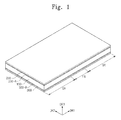
- FIG. 1 is a perspective view of a flexible display device according to example embodiments.
- FIG. 2A is a side view illustrating an unfolded structure of the flexible display device according to example embodiments
- FIG. 2B is a side view illustrating a folded structure of the flexible display device according to example embodiments.
- a flexible display device may include a flexible display panel 100, a first outer member 200, and a first adhesive member 200-A.
- the flexible display panel 100 may include a flexible substrate, signal lines disposed on the flexible substrate, and pixels electrically connected to the signal lines. An image may be displayed by the pixels, based on signals transmitted through the signal lines. The image may be displayed through a surface of the flexible display panel 100.
- the flexible display panel 100 may be bended or rolled to form a substantially curved surface, and it may be folded at a specific region.
- the flexible display panel 100 may include a folding region FA and a peripheral region SA.
- the flexible display panel 100 may include a pair of the peripheral regions SA and one folding region FA therebetween.
- Each of the folding and peripheral regions FA and SA may include some of the pixels. Further, the folding region FA and the peripheral regions SA may be configured to display an image without any discontinuity at interfaces between the folding and peripheral regions FA and SA.
- the folding region FA may be defined as a foldable region of the flexible display panel 100, while each of the peripheral regions SA may be defined as a region adjacent to the folding region FA.
- the peripheral regions SA may be flat or gently curved.
- the flexible display panel 100 may be fully folded in such a way that the pair of the peripheral regions SA face each other.
- a curvature radius CR of the flexible display panel 100 at the folding region FA may range from about 0.5 mm to about 10 mm.
- the first outer member 200 may be disposed on the surface of the flexible display panel 100.
- the first outer member 200 may include at least one of a polarizing plate, a touch screen, or a protection member.
- the polarizing plate, the touch screen, and the protection member may include a flexible element, such as a plastic substrate or a plastic film.
- first outer member 200 may further include a functional coating layer, such as anti-fingerprint coating layer or an anti-reflection coating layer.
- the first adhesive member 200-A may be disposed between the flexible display panel 100 and the first outer member 200 to adhere the first outer member 200 to the flexible display panel 100.
- the first adhesive member 200-A may include an ultraviolet curable resin.
- the ultraviolet curable resin may include at least one of urethane acrylate-based resins, epoxy acrylate-based resins, polyester-based resins, or polycarbonate-based resins.
- the first adhesive member includes a mixture of silicone resin and acrylic resin.
- a radical polymerization may start, when ultraviolet light is incident into the ultraviolet curable resin. Due to the incidence of the ultraviolet light, carbons in the ultraviolet curable resin may be changed from double bonds to single bonds. One cut chain of a double bond of carbons constituting a monomer or oligomer may form a polymer chain along with that of other monomer or oligomer. The more the polymer chain, the higher the cure level of the ultraviolet curable resin. The cure level of the ultraviolet curable resin may be proportional to the UV exposure time.
- the first adhesive member 200-A may include at least two regions, whose cure levels are different from each other.
- the first adhesive member 200-A may include a first region 200-AF corresponding to the folding region FA and a second region 200-AS corresponding to the peripheral region.
- the first region 200-AF may be lower than the second region 200-AS. Accordingly, it is possible to maintain the flexibility of the first region 200-AF, and thus, the first region 200-AF is not broken even when the flexible display panel 100 is folded.
- the first region 200-AF may have a tensile strain lower than the second region 200-AS.
- a conversion rate of the first region 200-AF is lower than that of the second region 200-AS, when the first region 200-AF has a lower cure level than the second region 200-AS as described above.
- the conversion rate may represent how many carbons in the ultraviolet curable resin are changed from double bonds to single bonds.
- the conversion rate may be measured by analyzing the first adhesive member 200-A using a Fourier transform infrared spectrometer (FT-IR) method.
- FT-IR Fourier transform infrared spectrometer
- the first region 200-AF may have a conversion rate ranging from about 50% to about 80%, and this may make it possible to achieve an adhesive strength higher than a desired value and maintain the flexible property.
- the second region 200-AS may have a conversion rate ranging from about 85% to 100%.
- the first adhesive member 200-A may have a thickness ranging from about 10 ⁇ m to about 200 ⁇ m.
- the display device may further include a second outer member 300 and a second adhesive member 300-A.
- the second outer member 300 may be disposed on other surface of the flexible display panel 100 facing the surface of the flexible display panel 100 in a thickness direction DR3.
- the second outer member 300 may include at least one of a polarizing plate or a protection member. Further, two or more outer members may be disposed on the other surface of the flexible display panel 100.
- the second adhesive member 300-A may be disposed between the flexible display panel 100 and the second outer member 300 to attach the second outer member 300 to the flexible display panel 100.
- the second adhesive member 300-A may include an ultraviolet curable resin.
- the second adhesive member 300-A may include at least two regions, whose cure levels are different from each other.
- the second adhesive member 300-A may include a third region 300-AF corresponding to the folding region FA and a fourth region 300-AS corresponding to the peripheral region.
- the third region 300-AF may be lower than the fourth region 300-AS.
- the third region 300-AF may have a conversion rate ranging from about 50% to about 80%, while the fourth region 300-AS may have a conversion rate ranging from about 85% to 100%.
- the second adhesive member 300-A may have a thickness ranging from about 10 ⁇ m to about 200 ⁇ m.
- FIG. 3 is an equivalent circuit diagram of a pixel in a flexible display panel according to example embodiments.
- FIG. 4 is a layout diagram of the pixel in the flexible display panel according to example embodiments.
- FIG. 5 is a sectional view taken along a line I-I' of FIG. 4
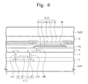
- FIG. 6 is a sectional view taken along a line II-II' of FIG. 4 .
- Image devices including pixels may be changed depending on the kind of flexible display panel.
- an organic light emitting display panel an organic light emitting diode may be used for the image device
- an electrophoresis display panel two electrodes and electrophoresis particles may be used to realize the image device.
- an electrowetting display panel two electrodes and electric ink may be used to realize the image device.
- an organic light emitting display panel hereinafter, referred to as a "display panel” will be described with reference to FIGS. 3 through 5 as an example of flexible display panel.
- the display panel 100 may include a base substrate SUB1, signal lines GL and DL, pixels PX, and an encapsulating substrate SUB2.
- a base substrate SUB1 signal lines GL and DL
- pixels PX pixels
- FIGS. 3 through 6 one of the pixel PX is illustrated as an example.
- the base substrate SUB1 may include a flexible plastic substrate.
- the pixel PX may include at least one transistor, at least one capacitor, and an organic light emitting diode.
- the signal lines GL and DL may include a gate line GL, a data line DL, and a power line KL.
- the encapsulating substrate SUB2 may also include a flexible plastic substrate. The encapsulating substrate SUB2 may be replaced with an encapsulating thin film in some embodiments.
- the gate line GL, the data line DL, the power line KL, and the pixel PX may be disposed on the base substrate SUB1.
- the pixel PX may include a first thin film transistor TFT1, a second thin film transistor TFT2, a capacitor Cap, and an organic light emitting diode OLED.
- a semiconductor pattern AL1 (hereinafter, referred as to a "first semiconductor pattern") for the first thin film transistor TFT1 and a semiconductor pattern AL2 (hereinafter, referred as to a "second semiconductor pattern") for the second thin film transistor TFT2 may be disposed on the base substrate SUB1.
- a first insulating layer 12 may be provided on the base substrate SUB1 to cover the first semiconductor pattern AL1 and the second semiconductor pattern AL2.
- the first insulating layer 12 may include an organic and/or inorganic layer.
- the first insulating layer 12 may include a plurality of thin films.
- a control electrode GE1 (hereinafter, referred as to a "first control electrode”) for the first thin film transistor TFT1 and a control electrode GE2 (hereinafter, referred as to a "second control electrode”) for the second thin film transistor TFT2 may be disposed on the first insulating layer 12.
- a first electrode CE1 of the capacitor Cap may be disposed on the first insulating layer 12.
- a second insulating layer 14 may be disposed on the first insulating layer 12 to cover the first and second control electrodes GE1 and GE2 and the first electrode CE1 of the capacitor.
- the second insulating layer 14 may include an organic and/or inorganic layer.
- the second insulating layer 14 may include a plurality of thin films.
- An input electrode SE1 (hereinafter, referred as to a "first input electrode”) and output electrode DE1 (hereinafter, referred as to a “first output electrode”) for the first thin film transistor TFT1 may be disposed on the second insulating layer 14.
- An input electrode SE2 (hereinafter, referred as to a "second input electrode”) and output electrode DE2 (hereinafter, referred as to a “second output electrode”) for the second thin film transistor TFT2 may be disposed on the second insulating layer 14.
- a second electrode CE2 of the capacitor Cap may be disposed on the second insulating layer 14.
- the first input electrode SE1 and the first output electrode DE1 may be connected to the first semiconductor pattern AL1 via a first through hole CH1 and a second through hole CH2, respectively, that are formed to penetrate the first insulating layer 12 and the second insulating layer 14.
- the first output electrode DE1 may be connected to the first electrode CE1 via a third through hole CH3 penetrating the second insulating layer 14.
- the second input electrode SE2 and the second output electrode DE2 may be connected to the second semiconductor pattern AL2 via a fourth through hole CH4 and a fifth through hole CH5, respectively, that are formed to penetrate the first insulating layer 12 and the second insulating layer 14.
- the first thin film transistor TFT1 and the second thin film transistor TFT2 may be configured to have a bottom-gate structure.
- a third insulating layer 16 may be disposed on the second insulating layer 14 to cover the first input electrode SE1, the first output electrode DE1, the second input electrode SE2, and the second output electrode DE2.
- the third insulating layer 16 may include an organic and/or inorganic layer.
- the third insulating layer 16 may include a plurality of thin films.
- a pixel-defining layer PXL and the organic light emitting diode OLED may be disposed on the third insulating layer 16.
- the organic light emitting diode OLED may include an anode AE, a first common layer CL1, an organic light emitting layer EML, a second common layer CL2, and a cathode CE, which may be sequentially stacked on the third insulating layer 16.
- the anode AE may be connected to the second output electrode DE2 via a sixth through hole CH6 that is formed to penetrate the third insulating layer 16.
- the anode AE and the cathode CE may be provided to have positions different from those shown in FIG. 6 .
- the anode AE may be provided on the third insulating layer 16.
- the pixel-defining layer PXL may include an opening OP exposing the anode AE.
- the first common layer CL1 may be provided on the anode AE.
- the first common layer CL1 may extend a light-emitting region delimited by the opening OP to a non-light-emitting region.
- the first common layer CL1 may be wholly provided on the top surface of the base substrate SUB1.
- the first common layer CL1 may include a hole injection layer.
- the first common layer CL1 may further include a hole transport layer.
- the organic light emitting layer EML may be provided on the first common layer CL1.
- the organic light emitting layer EML may be located on the opening OP.
- the second common layer CL2 may be provided on the organic light emitting layer EML.
- the second common layer CL2 may be wholly provided on the top surface of the base substrate SUB1, like the first common layer CL1.
- the second common layer CL2 may include an electron injection layer.
- the second common layer CL2 may further include an electron transport layer.
- the cathode CE may be provided on the second common layer CL2.
- the cathode CE may be wholly provided on the top surface of the base substrate SUB1.
- a fourth insulating layer 18 may be provided on the cathode CE.
- the fourth insulating layer 18 may include an organic and/or inorganic layer.
- the fourth insulating layer 18 may include a plurality of thin films.
- the encapsulating substrate SUB2 may be provided on the fourth insulating layer 18.
- FIG. 7 is a side view illustrating an unfolded structure of a flexible display device according to example embodiments.
- FIG. 8 is an enlarged view of a portion of FIG. 7 .
- a flexible display device will be described with reference to FIGS. 7 and 8 .
- the elements and features of this example embodiment that are similar to those previously shown and described will not be described in much further detail.
- a flexible display device (hereinafter, referred as to a “display device”) may include the flexible display panel 100, the first outer member 200, and the first adhesive member 200-A10.
- the flexible display panel 100 may be bended, folded, or rolled to form a substantially curved surface.
- the flexible display panel 100 may be an organic light emitting display panel, an electrophoresis display panel, or an electrowetting display panel.
- the flexible display panel 100 may be configured to display an image through a surface thereof.
- the first outer member 200 may be provided on the surface of the flexible display panel 100.
- the first adhesive member 200-A10 may be disposed between the flexible display panel 100 and the first outer member 200 to attach the first outer member 200 to the flexible display panel 100.
- the first adhesive member 200-A10 may include a mixture of silicone resin and acrylic resin.
- the first adhesive member 200-A10 may contain a silicone resin, which may be formed by catalytically reacting poly dimethyl siloxane (PDMS) with silicate resin at high temperature.
- PDMS poly dimethyl siloxane
- the acrylic resin may contain methyl acrylate, ethyl acrylate, n-propyl acrylate, isopropyl acrylate, n-butyl acrylate, t-butyl acrylate, sec-butyl acrylate, pentyl acrylate, 2-ethylhexyl acrylate, n-octyl acrylate, iso-octyl acrylate, iso-nonyl acrylate, isobornyl acrylate, or lauryl acrylate as a monomer component.
- the first adhesive member 200-A10 may contain about 40-60 part by weight of silicone resin and about 60-40 part by weight of acrylic resin.
- the first adhesive member 200-A10 may include about 50 part by weight of silicone resin and about 50 part by weight of acrylic resin.
- the first adhesive member 200-A10 may have a thickness ranging from about 10 ⁇ m to about 200 ⁇ m.
- the first adhesive member 200-A10 may not be damaged because it has both of the flexible property of the silicone resin and the adhesive property of the acrylic resin.
- the first outer member 200 may include a touch screen 210 disposed on the first adhesive member 200-A10 and a protection member 220 disposed on the touch screen 210.
- the protection member 220 may include a flexible plastic film.
- the protection member 220 may further include a functional coating layer, such as anti-fingerprint coating layer or an anti-reflection coating layer.
- the touch screen 210 and the protection member 220 may be jointed to each other by an adhesive member 220-A.
- the adhesive member 220-A may be formed of the same material as the first adhesive member 200-A10.
- the display device may further include a second outer member 300 and a second adhesive member 300-A10.
- the second outer member 300 may be disposed on the other side of the flexible display panel 100.
- the second adhesive member 300-A10 may be formed of the same material as the first adhesive member 200-A10.
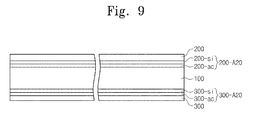
- FIG. 9 is a side view illustrating an unfolded structure of a flexible display device according to example embodiments.
- the flexible display device will be described with reference to FIG. 9 .
- the elements and features of this example that are similar to those previously shown and described will not be described in much further detail.
- a flexible display device (hereinafter, referred as to a "display device”) may include the flexible display panel 100, the first outer member 200, and a first adhesive member 200-A20.
- the flexible display panel 100 may be configured to display an image through a surface thereof.
- the first outer member 200 may be disposed on the surface of the flexible display panel 100.
- the first adhesive member 200-A20 may be disposed between the flexible display panel 100 and the first outer member 200 to attach the first outer member 200 to the flexible display panel 100.
- the first adhesive member 200-A20 may include a silicone resin layer 200-si and an acrylic resin layer 200-ac.
- the silicone resin layer 200-si may contain a silicone resin, which may be formed by catalytically reacting poly dimethyl siloxane (PDMS) with silicate resin at high temperature.
- PDMS poly dimethyl siloxane
- the acrylic resin layer 200-ac may contain methyl acrylate, ethyl acrylate, n-propyl acrylate, isopropyl acrylate, n-butyl acrylate, t-butyl acrylate, sec-butyl acrylate, pentyl acrylate, 2-ethylhexyl acrylate, n-octyl acrylate, iso-octyl acrylate, iso-nonyl acrylate, isobornyl acrylate, or lauryl acrylateas a monomer component.
- the first adhesive member 200-A10 may have a thickness ranging from about 10 ⁇ m to about 200 ⁇ m.
- a ratio in thickness of the silicone resin layer 200-si to the acrylic resin layer 200-ac may range from about 6:4 to about 4:6.
- the silicone resin layer 200-si and the acrylic resin layer 200-ac may have the same thickness.
- the first adhesive member 200-A20 may not be damaged because it has both of the flexible property of the silicone resin and the adhesive property of the acrylic resin.
- the display device may further include the second outer member 300 and a second adhesive member 300-A20.
- the second outer member 300 may be disposed on the other side of the flexible display panel 100.
- the second adhesive member 300-A20 may be formed of the same material as the first adhesive member 200-A20.
- the first adhesive member may include a first region corresponding to the folding region.
- the first region of the first adhesive member is more flexible than other regions.
- the cure level of the first region is lower than the other regions. Accordingly, even if the flexible display device is folded, it is possible to prevent the first adhesive member from being broken. Further, the flexible display device can be normally operated, even when it is repeatedly folded and unfolded.
- the first adhesive member has both the flexible property of the silicone resin and the adhesive property of the acrylic resin, and thus, even when the flexible display device is bended, folded, and/or rolled, it is possible to prevent the first adhesive member from being broken.
- a flexible display device comprising: a flexible display panel including a folding region and a peripheral region; a first outer member disposed on a surface of the flexible display panel; and a first adhesive member arranged to attach the first outer member to the flexible display panel, the first adhesive member comprising an ultraviolet curable resin, and first and second regions respectively corresponding to the folding and peripheral regions, wherein the ultraviolet curable resin of the first region has a conversion rate lower than a conversion rate of the ultraviolet curable resin of the second region.
- the first adhesive member includes a mixture of silicone resin and acrylic resin
- Embodiments of the invention also provide flexible display device, comprising: a flexible display panel; a first outer member disposed on a surface of the flexible display panel; and a first adhesive member attaching the first outer member to the flexible display panel and including silicone resin and acrylic resin.
- the first adhesive member includes a mixture of silicone resin and acrylic resin.
- the first adhesive member includes a silicone resin layer and an acrylic resin layer.
Landscapes
- Chemical & Material Sciences (AREA)
- Engineering & Computer Science (AREA)
- Physics & Mathematics (AREA)
- Chemical Kinetics & Catalysis (AREA)
- Theoretical Computer Science (AREA)
- Manufacturing & Machinery (AREA)
- Materials Engineering (AREA)
- Health & Medical Sciences (AREA)
- General Physics & Mathematics (AREA)
- Medicinal Chemistry (AREA)
- Polymers & Plastics (AREA)
- Organic Chemistry (AREA)
- Microelectronics & Electronic Packaging (AREA)
- Devices For Indicating Variable Information By Combining Individual Elements (AREA)
- Optics & Photonics (AREA)
- Electroluminescent Light Sources (AREA)
Abstract
Description
- The disclosure relates to a display device, and in particular, to a flexible display device.
- Recently, a bendable or foldable display device (hereinafter, referred as to a "flexible display device") has been developed. The flexible display device includes a flexible display panel and several functional parts.
- The functional parts are disposed on the flexible display panel. The functional parts may be bended or folded along with the flexible display panel.
- Example embodiments of the inventive concept provide a flexible display device capable of preventing a failure from occurring.
- A flexible display device may include a flexible display panel, a first outer member disposed on a surface of the flexible display panel, and a first adhesive member attaching the first outer member to the flexible display panel.
- The flexible display panel may include a folding region and a peripheral region. The first adhesive member may include an ultraviolet curable resin. The first adhesive member may include first and second regions respectively corresponding to the folding and peripheral regions. The ultraviolet curable resin of the first region may have a conversion rate lower than a conversion rate of the ultraviolet curable resin of the second region.
- The conversion rate of the ultraviolet curable resin of the first region ranges from about 50% to about 80%, and the conversion rate of the ultraviolet curable resin of the second region ranges from about 85% to 100%.
- The ultraviolet curable resin may include at least one of urethane acrylate-based resins, epoxy acrylate-based resins, polyester-based resins, or polycarbonate-based resins. The first adhesive member has a thickness ranging from about 10 µm to about 200 µm. The flexible display panel may be folded at the folding region with a curvature radius of about 0.5 to about 10 mm.
- The flexible display device may further include a second outer member disposed on another surface of the flexible display panel, and a second adhesive member attaching the second outer member to the flexible display panel. The second adhesive member may include an ultraviolet curable resin.
- The second adhesive member may include third and fourth regions corresponding to the folding and peripheral regions, respectively. The ultraviolet curable resin of the third region may have a conversion rate lower than a conversion rate of the ultraviolet curable resin of the fourth region.
- A flexible display device may include a flexible display panel, a first outer member disposed on a surface of the flexible display panel, and a first adhesive member attaching the first outer member to the flexible display panel.
- The first adhesive member may include a mixture of silicone resin and acrylic resin. The first adhesive member may include silicone resin of in 40-60 part by weight and acrylic resin in 60-40 part by weight.
- The first adhesive member may include a silicone resin layer and an acrylic resin layer. The silicone resin layer and the acrylic resin layer may have substantially the same thickness.
- According to an aspect of the invention, there is provided a flexible display device as set out in claim 1. Preferred features of this aspect are set out in claims 2 to 7.
- According to another aspect of the invention, there is provided a flexible display device as set out in claim 8. Preferred features of this aspect are set out in claims 9 to 15.
- Example embodiments will be more clearly understood from the following brief description taken in conjunction with the accompanying drawings. The accompanying drawings represent non-limiting, example embodiments as described herein.
-
FIG. 1 is a perspective view of a flexible display device according to example embodiments. -
FIG. 2A is a side view illustrating an unfolded structure of the flexible display device according to example embodiments. -
FIG. 2B is a side view illustrating a folded structure of the flexible display device according to example embodiments. -
FIG. 3 is an equivalent circuit diagram of a pixel in a flexible display panel according to example embodiments. -
FIG. 4 is a layout diagram of the pixel in the flexible display panel according to example embodiments. -
FIG. 5 is a sectional view taken along a line I-I' ofFIG. 4 . -
FIG. 6 is a sectional view taken along a line II-II' ofFIG. 4 . -
FIG. 7 is a side view illustrating an unfolded structure of a flexible display device according to example embodiments. -
FIG. 8 is an enlarged view of a portion ofFIG. 7 . -
FIG. 9 is a side view illustrating an unfolded structure of a flexible display device according to example embodiments. - It should be noted that these figures are intended to illustrate the general characteristics of methods, structure and/or materials utilized in certain example embodiments and to supplement the written description provided below. These drawings are not, however, to scale and may not precisely reflect the precise structural or performance characteristics of any given embodiment, and should not be interpreted as defining or limiting the range of values or properties encompassed by example embodiments. For example, the relative thicknesses and positioning of molecules, layers, regions and/or structural elements may be reduced or exaggerated for clarity. The use of similar or identical reference numbers in the various drawings is intended to indicate the presence of a similar or identical element or feature.
- Example embodiments will now be described more fully with reference to the accompanying drawings, in which example embodiments are shown. Example embodiments may, however, be embodied in many different forms and should not be construed as being limited to the embodiments set forth herein; rather, these embodiments are provided so that this disclosure will be thorough and complete, and will fully convey the concept of example embodiments to those of ordinary skill in the art. In the drawings, the thicknesses of layers and regions may be exaggerated for clarity. Like reference numerals in the drawings generally denote like elements, and thus their description will be omitted.
- It will be understood that when an element is referred to as being "connected" or "coupled" to another element, it can be directly connected or coupled to the other element or intervening elements may be present. In contrast, when an element is referred to as being "directly connected" or "directly coupled" to another element, there are no intervening elements present. As used herein the term "and/or" includes any and all combinations of one or more of the associated listed items. Other words used to describe the relationship between elements or layers should be interpreted in a like fashion (e.g., "between" versus "directly between," "adjacent" versus "directly adjacent," "on" versus "directly on").
- It will be understood that, although the terms "first", "second", and the like may be used herein to describe various elements, components, regions, layers and/or sections, these elements, components, regions, layers and/or sections should not be limited by these terms. These terms are only used to distinguish one element, component, region, layer or section from another element, component, region, layer or section. Thus, a first element, component, region, layer or section discussed below could be termed a second element, component, region, layer or section without departing from the teachings of example embodiments.
- Spatially relative terms, such as "beneath," "below," "lower," "above," "upper" and the like, may be used herein for ease of description to describe one element or feature's relationship to another element(s) or feature(s) as illustrated in the figures. It will be understood that the spatially relative terms are intended to encompass different orientations of the device in use or operation in addition to the orientation depicted in the figures. For example, if the device in the figures is turned over, elements described as "below" or "beneath" other elements or features would then be oriented "above" the other elements or features. Thus, the exemplary term "below" can encompass both an orientation of above and below. The device may be otherwise oriented (rotated 90 degrees or at other orientations) and the spatially relative descriptors used herein interpreted accordingly.
- The terminology used herein is for the purpose of describing particular embodiments only and is not intended to be limiting of example embodiments. As used herein, the singular forms "a," "an" and "the" are intended to include the plural forms as well, unless the context clearly indicates otherwise. It will be further understood that the terms "comprises", "comprising", "includes" and/or "including," if used herein, specify the presence of stated features, integers, steps, operations, elements and/or components, but do not preclude the presence or addition of one or more other features, integers, steps, operations, elements, components and/or groups thereof. Unless otherwise defined, all terms (including technical and scientific terms) used herein have the same meaning as commonly understood by one of ordinary skill in the art to which example embodiments belong. It will be further understood that terms, such as those defined in commonly-used dictionaries, should be interpreted as having a meaning that is consistent with their meaning in the context of the relevant art and will not be interpreted in an idealized or overly formal sense unless expressly so defined herein.
-
FIG. 1 is a perspective view of a flexible display device according to example embodiments.FIG. 2A is a side view illustrating an unfolded structure of the flexible display device according to example embodiments, andFIG. 2B is a side view illustrating a folded structure of the flexible display device according to example embodiments. - According to example embodiments, as shown in
FIGS. 1 ,2A and 2B , a flexible display device (hereinafter, also referred as to a "display device") may include aflexible display panel 100, a firstouter member 200, and a first adhesive member 200-A. - The
flexible display panel 100 may include a flexible substrate, signal lines disposed on the flexible substrate, and pixels electrically connected to the signal lines. An image may be displayed by the pixels, based on signals transmitted through the signal lines. The image may be displayed through a surface of theflexible display panel 100. - The
flexible display panel 100 may be bended or rolled to form a substantially curved surface, and it may be folded at a specific region. When viewed in a plane defined by a first direction DR1 and second direction DR2, theflexible display panel 100 may include a folding region FA and a peripheral region SA. In the example shown inFIGS. 1 ,2A and 2B , theflexible display panel 100 may include a pair of the peripheral regions SA and one folding region FA therebetween. - Each of the folding and peripheral regions FA and SA may include some of the pixels. Further, the folding region FA and the peripheral regions SA may be configured to display an image without any discontinuity at interfaces between the folding and peripheral regions FA and SA. The folding region FA may be defined as a foldable region of the
flexible display panel 100, while each of the peripheral regions SA may be defined as a region adjacent to the folding region FA. The peripheral regions SA may be flat or gently curved. - As shown in
FIG. 2B , theflexible display panel 100 may be fully folded in such a way that the pair of the peripheral regions SA face each other. A curvature radius CR of theflexible display panel 100 at the folding region FA may range from about 0.5 mm to about 10 mm. - The first
outer member 200 may be disposed on the surface of theflexible display panel 100. The firstouter member 200 may include at least one of a polarizing plate, a touch screen, or a protection member. The polarizing plate, the touch screen, and the protection member may include a flexible element, such as a plastic substrate or a plastic film. - Further, at least two outer members may be disposed on the surface of the
flexible display panel 100. In addition, the firstouter member 200 may further include a functional coating layer, such as anti-fingerprint coating layer or an anti-reflection coating layer. - The first adhesive member 200-A may be disposed between the
flexible display panel 100 and the firstouter member 200 to adhere the firstouter member 200 to theflexible display panel 100. - The first adhesive member 200-A may include an ultraviolet curable resin. The ultraviolet curable resin may include at least one of urethane acrylate-based resins, epoxy acrylate-based resins, polyester-based resins, or polycarbonate-based resins.
- In some embodiments, the first adhesive member includes a mixture of silicone resin and acrylic resin.
- A radical polymerization may start, when ultraviolet light is incident into the ultraviolet curable resin. Due to the incidence of the ultraviolet light, carbons in the ultraviolet curable resin may be changed from double bonds to single bonds. One cut chain of a double bond of carbons constituting a monomer or oligomer may form a polymer chain along with that of other monomer or oligomer. The more the polymer chain, the higher the cure level of the ultraviolet curable resin. The cure level of the ultraviolet curable resin may be proportional to the UV exposure time.
- The first adhesive member 200-A may include at least two regions, whose cure levels are different from each other. The first adhesive member 200-A may include a first region 200-AF corresponding to the folding region FA and a second region 200-AS corresponding to the peripheral region.
- In terms of a cured level, the first region 200-AF may be lower than the second region 200-AS. Accordingly, it is possible to maintain the flexibility of the first region 200-AF, and thus, the first region 200-AF is not broken even when the
flexible display panel 100 is folded. The first region 200-AF may have a tensile strain lower than the second region 200-AS. - A conversion rate of the first region 200-AF is lower than that of the second region 200-AS, when the first region 200-AF has a lower cure level than the second region 200-AS as described above. For example, the conversion rate may represent how many carbons in the ultraviolet curable resin are changed from double bonds to single bonds.
- The conversion rate may be measured by analyzing the first adhesive member 200-A using a Fourier transform infrared spectrometer (FT-IR) method. In example embodiments, the first region 200-AF may have a conversion rate ranging from about 50% to about 80%, and this may make it possible to achieve an adhesive strength higher than a desired value and maintain the flexible property.
- The second region 200-AS may have a conversion rate ranging from about 85% to 100%. The first adhesive member 200-A may have a thickness ranging from about 10 µm to about 200 µm.
- As shown in
FIGS. 1 ,2A, and 2B , the display device may further include a secondouter member 300 and a second adhesive member 300-A. - The second
outer member 300 may be disposed on other surface of theflexible display panel 100 facing the surface of theflexible display panel 100 in a thickness direction DR3. - The second
outer member 300 may include at least one of a polarizing plate or a protection member. Further, two or more outer members may be disposed on the other surface of theflexible display panel 100. - The second adhesive member 300-A may be disposed between the
flexible display panel 100 and the secondouter member 300 to attach the secondouter member 300 to theflexible display panel 100. - The second adhesive member 300-A may include an ultraviolet curable resin. The second adhesive member 300-A may include at least two regions, whose cure levels are different from each other. For example, the second adhesive member 300-A may include a third region 300-AF corresponding to the folding region FA and a fourth region 300-AS corresponding to the peripheral region.
- In terms of a cured level, the third region 300-AF may be lower than the fourth region 300-AS. The third region 300-AF may have a conversion rate ranging from about 50% to about 80%, while the fourth region 300-AS may have a conversion rate ranging from about 85% to 100%. The second adhesive member 300-A may have a thickness ranging from about 10 µm to about 200 µm.
-
FIG. 3 is an equivalent circuit diagram of a pixel in a flexible display panel according to example embodiments.FIG. 4 is a layout diagram of the pixel in the flexible display panel according to example embodiments.FIG. 5 is a sectional view taken along a line I-I' ofFIG. 4 , andFIG. 6 is a sectional view taken along a line II-II' ofFIG. 4 . - Image devices including pixels may be changed depending on the kind of flexible display panel. For example, for an organic light emitting display panel, an organic light emitting diode may be used for the image device, and for an electrophoresis display panel, two electrodes and electrophoresis particles may be used to realize the image device. For an electrowetting display panel, two electrodes and electric ink may be used to realize the image device. Hereinafter, an organic light emitting display panel (hereinafter, referred to as a "display panel") will be described with reference to
FIGS. 3 through 5 as an example of flexible display panel. - The
display panel 100 may include a base substrate SUB1, signal lines GL and DL, pixels PX, and an encapsulating substrate SUB2. InFIGS. 3 through 6 , one of the pixel PX is illustrated as an example. - The base substrate SUB1 may include a flexible plastic substrate. The pixel PX may include at least one transistor, at least one capacitor, and an organic light emitting diode. The signal lines GL and DL may include a gate line GL, a data line DL, and a power line KL. The encapsulating substrate SUB2 may also include a flexible plastic substrate. The encapsulating substrate SUB2 may be replaced with an encapsulating thin film in some embodiments.
- The gate line GL, the data line DL, the power line KL, and the pixel PX may be disposed on the base substrate SUB1. The pixel PX may include a first thin film transistor TFT1, a second thin film transistor TFT2, a capacitor Cap, and an organic light emitting diode OLED.
- A semiconductor pattern AL1 (hereinafter, referred as to a "first semiconductor pattern") for the first thin film transistor TFT1 and a semiconductor pattern AL2 (hereinafter, referred as to a "second semiconductor pattern") for the second thin film transistor TFT2 may be disposed on the base substrate SUB1. A first insulating
layer 12 may be provided on the base substrate SUB1 to cover the first semiconductor pattern AL1 and the second semiconductor pattern AL2. The first insulatinglayer 12 may include an organic and/or inorganic layer. The first insulatinglayer 12 may include a plurality of thin films. - A control electrode GE1 (hereinafter, referred as to a "first control electrode") for the first thin film transistor TFT1 and a control electrode GE2 (hereinafter, referred as to a "second control electrode") for the second thin film transistor TFT2 may be disposed on the first insulating
layer 12. A first electrode CE1 of the capacitor Cap may be disposed on the first insulatinglayer 12. - A second insulating
layer 14 may be disposed on the first insulatinglayer 12 to cover the first and second control electrodes GE1 and GE2 and the first electrode CE1 of the capacitor. The second insulatinglayer 14 may include an organic and/or inorganic layer. The second insulatinglayer 14 may include a plurality of thin films. - An input electrode SE1 (hereinafter, referred as to a "first input electrode") and output electrode DE1 (hereinafter, referred as to a "first output electrode") for the first thin film transistor TFT1 may be disposed on the second insulating
layer 14. An input electrode SE2 (hereinafter, referred as to a "second input electrode") and output electrode DE2 (hereinafter, referred as to a "second output electrode") for the second thin film transistor TFT2 may be disposed on the second insulatinglayer 14. A second electrode CE2 of the capacitor Cap may be disposed on the second insulatinglayer 14. - The first input electrode SE1 and the first output electrode DE1 may be connected to the first semiconductor pattern AL1 via a first through hole CH1 and a second through hole CH2, respectively, that are formed to penetrate the first insulating
layer 12 and the second insulatinglayer 14. The first output electrode DE1 may be connected to the first electrode CE1 via a third through hole CH3 penetrating the second insulatinglayer 14. The second input electrode SE2 and the second output electrode DE2 may be connected to the second semiconductor pattern AL2 via a fourth through hole CH4 and a fifth through hole CH5, respectively, that are formed to penetrate the first insulatinglayer 12 and the second insulatinglayer 14. In some embodiments, the first thin film transistor TFT1 and the second thin film transistor TFT2 may be configured to have a bottom-gate structure. - A third insulating
layer 16 may be disposed on the second insulatinglayer 14 to cover the first input electrode SE1, the first output electrode DE1, the second input electrode SE2, and the second output electrode DE2. The third insulatinglayer 16 may include an organic and/or inorganic layer. The third insulatinglayer 16 may include a plurality of thin films. - A pixel-defining layer PXL and the organic light emitting diode OLED may be disposed on the third insulating
layer 16. The organic light emitting diode OLED may include an anode AE, a first common layer CL1, an organic light emitting layer EML, a second common layer CL2, and a cathode CE, which may be sequentially stacked on the third insulatinglayer 16. The anode AE may be connected to the second output electrode DE2 via a sixth through hole CH6 that is formed to penetrate the third insulatinglayer 16. Depending on a light-emitting direction of the organic light emitting diode OLED, the anode AE and the cathode CE may be provided to have positions different from those shown inFIG. 6 . - The anode AE may be provided on the third insulating
layer 16. The pixel-defining layer PXL may include an opening OP exposing the anode AE. The first common layer CL1 may be provided on the anode AE. The first common layer CL1 may extend a light-emitting region delimited by the opening OP to a non-light-emitting region. For example, the first common layer CL1 may be wholly provided on the top surface of the base substrate SUB1. The first common layer CL1 may include a hole injection layer. The first common layer CL1 may further include a hole transport layer. - The organic light emitting layer EML may be provided on the first common layer CL1. The organic light emitting layer EML may be located on the opening OP. The second common layer CL2 may be provided on the organic light emitting layer EML. The second common layer CL2 may be wholly provided on the top surface of the base substrate SUB1, like the first common layer CL1. The second common layer CL2 may include an electron injection layer. The second common layer CL2 may further include an electron transport layer. The cathode CE may be provided on the second common layer CL2. The cathode CE may be wholly provided on the top surface of the base substrate SUB1.
- A fourth insulating
layer 18 may be provided on the cathode CE. The fourth insulatinglayer 18 may include an organic and/or inorganic layer. The fourth insulatinglayer 18 may include a plurality of thin films. The encapsulating substrate SUB2 may be provided on the fourth insulatinglayer 18. -
FIG. 7 is a side view illustrating an unfolded structure of a flexible display device according to example embodiments.FIG. 8 is an enlarged view of a portion ofFIG. 7 . Hereinafter, a flexible display device will be described with reference toFIGS. 7 and 8 . For the sake of brevity, the elements and features of this example embodiment that are similar to those previously shown and described will not be described in much further detail. - A flexible display device (hereinafter, referred as to a "display device") may include the
flexible display panel 100, the firstouter member 200, and the first adhesive member 200-A10. - The
flexible display panel 100 may be bended, folded, or rolled to form a substantially curved surface. Theflexible display panel 100 may be an organic light emitting display panel, an electrophoresis display panel, or an electrowetting display panel. - The
flexible display panel 100 may be configured to display an image through a surface thereof. The firstouter member 200 may be provided on the surface of theflexible display panel 100. The first adhesive member 200-A10 may be disposed between theflexible display panel 100 and the firstouter member 200 to attach the firstouter member 200 to theflexible display panel 100. - The first adhesive member 200-A10 may include a mixture of silicone resin and acrylic resin. The first adhesive member 200-A10 may contain a silicone resin, which may be formed by catalytically reacting poly dimethyl siloxane (PDMS) with silicate resin at high temperature.
- The acrylic resin may contain methyl acrylate, ethyl acrylate, n-propyl acrylate, isopropyl acrylate, n-butyl acrylate, t-butyl acrylate, sec-butyl acrylate, pentyl acrylate, 2-ethylhexyl acrylate, n-octyl acrylate, iso-octyl acrylate, iso-nonyl acrylate, isobornyl acrylate, or lauryl acrylate as a monomer component.
- The first adhesive member 200-A10 may contain about 40-60 part by weight of silicone resin and about 60-40 part by weight of acrylic resin. For example, the first adhesive member 200-A10 may include about 50 part by weight of silicone resin and about 50 part by weight of acrylic resin. The first adhesive member 200-A10 may have a thickness ranging from about 10 µm to about 200 µm.
- Even when the display device is bended, folded, and/or rolled, the first adhesive member 200-A10 may not be damaged because it has both of the flexible property of the silicone resin and the adhesive property of the acrylic resin.
- As shown in
FIG. 8 , the firstouter member 200 may include atouch screen 210 disposed on the first adhesive member 200-A10 and aprotection member 220 disposed on thetouch screen 210. Theprotection member 220 may include a flexible plastic film. In addition, theprotection member 220 may further include a functional coating layer, such as anti-fingerprint coating layer or an anti-reflection coating layer. - The
touch screen 210 and theprotection member 220 may be jointed to each other by an adhesive member 220-A. The adhesive member 220-A may be formed of the same material as the first adhesive member 200-A10. - Referring back to
FIG. 7 , the display device may further include a secondouter member 300 and a second adhesive member 300-A10. The secondouter member 300 may be disposed on the other side of theflexible display panel 100. The second adhesive member 300-A10 may be formed of the same material as the first adhesive member 200-A10. -
FIG. 9 is a side view illustrating an unfolded structure of a flexible display device according to example embodiments. Hereinafter, the flexible display device will be described with reference toFIG. 9 . For the sake of brevity, the elements and features of this example that are similar to those previously shown and described will not be described in much further detail. - A flexible display device (hereinafter, referred as to a "display device") may include the
flexible display panel 100, the firstouter member 200, and a first adhesive member 200-A20. - The
flexible display panel 100 may be configured to display an image through a surface thereof. The firstouter member 200 may be disposed on the surface of theflexible display panel 100. The first adhesive member 200-A20 may be disposed between theflexible display panel 100 and the firstouter member 200 to attach the firstouter member 200 to theflexible display panel 100. - The first adhesive member 200-A20 may include a silicone resin layer 200-si and an acrylic resin layer 200-ac. The silicone resin layer 200-si may contain a silicone resin, which may be formed by catalytically reacting poly dimethyl siloxane (PDMS) with silicate resin at high temperature.
- The acrylic resin layer 200-ac may contain methyl acrylate, ethyl acrylate, n-propyl acrylate, isopropyl acrylate, n-butyl acrylate, t-butyl acrylate, sec-butyl acrylate, pentyl acrylate, 2-ethylhexyl acrylate, n-octyl acrylate, iso-octyl acrylate, iso-nonyl acrylate, isobornyl acrylate, or lauryl acrylateas a monomer component.
- The first adhesive member 200-A10 may have a thickness ranging from about 10 µm to about 200 µm. A ratio in thickness of the silicone resin layer 200-si to the acrylic resin layer 200-ac may range from about 6:4 to about 4:6. The silicone resin layer 200-si and the acrylic resin layer 200-ac may have the same thickness.
- Even when the display device is bended, folded, and/or rolled, the first adhesive member 200-A20 may not be damaged because it has both of the flexible property of the silicone resin and the adhesive property of the acrylic resin.
- As shown in
FIG. 9 , the display device may further include the secondouter member 300 and a second adhesive member 300-A20. The secondouter member 300 may be disposed on the other side of theflexible display panel 100. The second adhesive member 300-A20 may be formed of the same material as the first adhesive member 200-A20. - According to example embodiments, the first adhesive member may include a first region corresponding to the folding region. The first region of the first adhesive member is more flexible than other regions. In other words, the cure level of the first region is lower than the other regions. Accordingly, even if the flexible display device is folded, it is possible to prevent the first adhesive member from being broken. Further, the flexible display device can be normally operated, even when it is repeatedly folded and unfolded.
- The first adhesive member has both the flexible property of the silicone resin and the adhesive property of the acrylic resin, and thus, even when the flexible display device is bended, folded, and/or rolled, it is possible to prevent the first adhesive member from being broken.
- As discussed, embodiments of the invention provide a flexible display device, comprising: a flexible display panel including a folding region and a peripheral region; a first outer member disposed on a surface of the flexible display panel; and a first adhesive member arranged to attach the first outer member to the flexible display panel, the first adhesive member comprising an ultraviolet curable resin, and first and second regions respectively corresponding to the folding and peripheral regions, wherein the ultraviolet curable resin of the first region has a conversion rate lower than a conversion rate of the ultraviolet curable resin of the second region. In some embodiments, the first adhesive member includes a mixture of silicone resin and acrylic resin
- Embodiments of the invention also provide flexible display device, comprising: a flexible display panel; a first outer member disposed on a surface of the flexible display panel; and a first adhesive member attaching the first outer member to the flexible display panel and including silicone resin and acrylic resin. In some embodiments, the first adhesive member includes a mixture of silicone resin and acrylic resin. In some embodiments the first adhesive member includes a silicone resin layer and an acrylic resin layer.
- While example embodiments of the inventive concepts have been particularly shown and described, it will be understood by one of ordinary skill in the art that variations in form and detail may be made therein without departing from the scope of the attached claims.
Claims (15)
- A flexible display device, comprising:a flexible display panel including a folding region and a peripheral region;a first outer member disposed on a surface of the flexible display panel; anda first adhesive member arranged to attach the first outer member to the flexible display panel, the first adhesive member comprising an ultraviolet curable resin, and first and second regions respectively corresponding to the folding and peripheral regions,wherein the ultraviolet curable resin of the first region has a conversion rate lower than a conversion rate of the ultraviolet curable resin of the second region.
- The flexible display device of claim 1, wherein the conversion rate of the ultraviolet curable resin of the first region ranges from about 50% to about 80%, and
the conversion rate of the ultraviolet curable resin of the second region ranges from about 85% to 100%. - The flexible display device of claim 2, wherein the ultraviolet curable resin includes at least one of an urethane acrylate-based resin, an epoxy acrylate-based resin, a polyester-based resin, or a polycarbonate-based resin.
- The flexible display device of claim 2 or 3, wherein the first adhesive member has a thickness ranging from about 10 µm to about 200 µm.
- The flexible display device of any one of claims 2 to 4, wherein the flexible display panel is folded at the folding region with a curvature radius of about 0.5 to about 10 mm.
- The flexible display device of any one of claims 1 to 5, further comprising:a second outer member disposed on another surface of the flexible display panel; anda second adhesive member attaching the second outer member to the flexible display panel and including an ultraviolet curable resin.
- The flexible display device of claim 6, wherein the second adhesive member includes third and fourth regions corresponding to the folding and peripheral regions, respectively, and
the ultraviolet curable resin of the third region has a conversion rate lower than a conversion rate of the ultraviolet curable resin of the fourth region. - A flexible display device, comprising:a flexible display panel;a first outer member disposed on a surface of the flexible display panel; anda first adhesive member attaching the first outer member to the flexible display panel and including silicone resin and acrylic resin.
- The flexible display device of claim 8, wherein the first adhesive member includes a mixture of silicone resin and acrylic resin.
- The flexible display device of claim 8 or 9, wherein the first adhesive member includes silicone resin in 40-60 part by weight and acrylic resin in 60-40 part by weight;
optionally wherein the first adhesive member includes silicone resin in 50 part by weight and acrylic resin in 50 part by weight. - The flexible display device of any one of claims 8 to 10, wherein the first adhesive member has a thickness ranging from about 10 µm to about 200 µm.
- The flexible display device of any one of claims 8 to 11, further comprising:a second outer member disposed on another surface of the flexible display panel; anda second adhesive member attaching the second outer member to the flexible display panel and including a mixture of silicone resin and acrylic resin.
- The flexible display device of claim 12, wherein the respective weight percentage of the mixture of silicone resin and acrylic resin in the second outer member is substantially the same as the mixture of silicone resin and acrylic resin in the first outer member.
- The flexible display device of claim 8, wherein the first adhesive member includes a silicone resin layer and an acrylic resin layer.
- The flexible display device of claim 14, wherein the silicone resin layer and the acrylic resin layer have substantially the same thickness.
Applications Claiming Priority (1)
| Application Number | Priority Date | Filing Date | Title |
|---|---|---|---|
| KR1020130091008A KR102127791B1 (en) | 2013-07-31 | 2013-07-31 | Flexible display device |
Publications (3)
| Publication Number | Publication Date |
|---|---|
| EP2833426A2 true EP2833426A2 (en) | 2015-02-04 |
| EP2833426A3 EP2833426A3 (en) | 2015-06-17 |
| EP2833426B1 EP2833426B1 (en) | 2019-09-04 |
Family
ID=50072975
Family Applications (1)
| Application Number | Title | Priority Date | Filing Date |
|---|---|---|---|
| EP14154706.7A Active EP2833426B1 (en) | 2013-07-31 | 2014-02-11 | Flexible display device |
Country Status (5)
| Country | Link |
|---|---|
| US (2) | US20150036269A1 (en) |
| EP (1) | EP2833426B1 (en) |
| JP (1) | JP6434711B2 (en) |
| KR (1) | KR102127791B1 (en) |
| CN (1) | CN104347007A (en) |
Cited By (7)
| Publication number | Priority date | Publication date | Assignee | Title |
|---|---|---|---|---|
| EP2894672A1 (en) * | 2014-01-13 | 2015-07-15 | Samsung Display Co., Ltd. | Flexible display device |
| CN107180850A (en) * | 2016-03-11 | 2017-09-19 | 三星显示有限公司 | Flexible display device |
| CN107230693A (en) * | 2016-03-25 | 2017-10-03 | 三星显示有限公司 | Flexible display device |
| EP3483707A1 (en) * | 2017-09-29 | 2019-05-15 | Samsung Display Co., Ltd. | Electronic display device |
| US10763314B2 (en) | 2015-12-28 | 2020-09-01 | 3M Innovative Properties Company | Flexible electronic device with fluid cavity design |
| US11101333B2 (en) | 2015-07-23 | 2021-08-24 | Semiconductor Energy Laboratory Co., Ltd. | Display device, module, and electronic device |
| US11404655B2 (en) | 2018-03-30 | 2022-08-02 | Samsung Display Co., Ltd. | Display device |
Families Citing this family (22)
| Publication number | Priority date | Publication date | Assignee | Title |
|---|---|---|---|---|
| JP6419608B2 (en) * | 2015-03-12 | 2018-11-07 | 株式会社ジャパンディスプレイ | Display device |
| KR102561880B1 (en) * | 2015-06-03 | 2023-08-02 | 쓰리엠 이노베이티브 프로퍼티즈 컴파니 | Flexible Display with Stiff Layer for Neutral Plane Adjustment |
| KR102399568B1 (en) * | 2015-09-23 | 2022-05-19 | 삼성디스플레이 주식회사 | Foldable display apparatus and the manufacturing method thereof |
| KR102665790B1 (en) * | 2016-01-14 | 2024-05-14 | 삼성디스플레이 주식회사 | Display panel and method of manufacturing the same |
| CN109844700A (en) | 2016-10-31 | 2019-06-04 | 富士胶片株式会社 | Laminates for touch panels, flexible devices, organic electroluminescence display devices |
| KR102731599B1 (en) * | 2016-11-07 | 2024-11-22 | 삼성디스플레이 주식회사 | Glass substrate, manufacturing method of the same, and display device having the same |
| JP2019003099A (en) * | 2017-06-16 | 2019-01-10 | 株式会社ジャパンディスプレイ | Display device manufacturing method and display device |
| KR102475857B1 (en) * | 2017-09-18 | 2022-12-12 | 삼성디스플레이 주식회사 | Flexible display device |
| CN107799011B (en) * | 2017-11-10 | 2019-11-05 | 武汉华星光电半导体显示技术有限公司 | Display module, the glue spreading method of display module and display device |
| US20190144714A1 (en) * | 2017-11-10 | 2019-05-16 | Wuhan China Star Optoelectronics Semiconductor Display Technology Co., Ltd. | Display module and coating glue method thereof and display device |
| CN107958920B (en) * | 2017-11-23 | 2020-10-09 | 合肥鑫晟光电科技有限公司 | Flexible display panel, flexible display device and preparation method thereof |
| WO2019106480A1 (en) | 2017-11-30 | 2019-06-06 | 株式会社半導体エネルギー研究所 | Display panel, display device, input/output device, and information processing device |
| CN108091612B (en) * | 2017-12-07 | 2020-11-24 | 深圳市华星光电半导体显示技术有限公司 | Array substrate and preparation method thereof |
| CN109065505B (en) * | 2018-08-10 | 2021-01-15 | 武汉华星光电半导体显示技术有限公司 | Display panel and manufacturing method thereof |
| KR102575599B1 (en) * | 2018-09-12 | 2023-09-05 | 엘지디스플레이 주식회사 | Flexible display panel and method of fabricating the same |
| KR102586636B1 (en) * | 2018-10-11 | 2023-10-11 | 삼성디스플레이 주식회사 | Foldable display device |
| CN110429123B (en) | 2019-08-12 | 2022-03-04 | 京东方科技集团股份有限公司 | Display panel, method for manufacturing the same, and display device |
| CN110570761A (en) * | 2019-08-15 | 2019-12-13 | 武汉华星光电半导体显示技术有限公司 | Flexible display module and flexible display device |
| KR102902139B1 (en) * | 2020-07-29 | 2025-12-18 | 엘지디스플레이 주식회사 | Flexible display device |
| KR20220075110A (en) * | 2020-11-27 | 2022-06-07 | 삼성디스플레이 주식회사 | Display device |
| JP7374949B2 (en) * | 2021-03-30 | 2023-11-07 | キヤノン株式会社 | Semiconductor devices, display devices, photoelectric conversion devices, electronic devices, lighting devices, mobile objects, and methods for manufacturing semiconductor devices |
| US12196991B2 (en) * | 2021-12-10 | 2025-01-14 | Wuhan China Star Optoelectronics Semiconductor Display Technology Co., Ltd. | Display device |
Family Cites Families (19)
| Publication number | Priority date | Publication date | Assignee | Title |
|---|---|---|---|---|
| US5972152A (en) * | 1997-05-16 | 1999-10-26 | Micron Communications, Inc. | Methods of fixturing flexible circuit substrates and a processing carrier, processing a flexible circuit and processing a flexible circuit substrate relative to a processing carrier |
| JP2000234064A (en) * | 1999-02-16 | 2000-08-29 | Okura Ind Co Ltd | Elastic curable resin composition |
| JP2002297066A (en) * | 2001-03-30 | 2002-10-09 | Sanyo Electric Co Ltd | Electroluminescence display device and manufacturing method therefor |
| JP4567941B2 (en) * | 2001-12-28 | 2010-10-27 | 株式会社半導体エネルギー研究所 | Method for manufacturing semiconductor device and method for manufacturing display device |
| JP5117422B2 (en) * | 2008-07-15 | 2013-01-16 | 富士フイルム株式会社 | Light emitting device and manufacturing method thereof |
| US8570470B2 (en) * | 2008-08-20 | 2013-10-29 | Lg Chem, Ltd. | Adhesive agent |
| JP2011003522A (en) * | 2008-10-16 | 2011-01-06 | Semiconductor Energy Lab Co Ltd | Flexible light-emitting device, electronic equipment, and method of manufacturing flexible light-emitting device |
| KR101860692B1 (en) * | 2009-05-02 | 2018-05-23 | 가부시키가이샤 한도오따이 에네루기 켄큐쇼 | Display panel |
| KR101155907B1 (en) * | 2009-06-04 | 2012-06-20 | 삼성모바일디스플레이주식회사 | Organic light emitting diode display and method for manufacturing the same |
| US8576209B2 (en) * | 2009-07-07 | 2013-11-05 | Semiconductor Energy Laboratory Co., Ltd. | Display device |
| JP5446790B2 (en) * | 2009-12-02 | 2014-03-19 | セイコーエプソン株式会社 | Electro-optical device and electronic apparatus |
| JP5406068B2 (en) * | 2010-02-12 | 2014-02-05 | トッパン・フォームズ株式会社 | Manufacturing method of electronic display panel |
| KR101821727B1 (en) * | 2010-04-16 | 2018-01-24 | 플렉스 라이팅 투 엘엘씨 | Front illumination device comprising a film-based lightguide |
| JP2012080959A (en) * | 2010-10-07 | 2012-04-26 | Olympus Corp | Needle-type sensor |
| JP5664207B2 (en) * | 2010-12-16 | 2015-02-04 | セイコーエプソン株式会社 | Information display terminal |
| KR101801352B1 (en) * | 2011-01-18 | 2017-11-27 | 삼성디스플레이 주식회사 | flat panel display device and method of manufacturing thereof |
| WO2012173397A2 (en) * | 2011-06-15 | 2012-12-20 | Kolon Industries, Inc. | Liti donor film |
| US10061356B2 (en) * | 2011-06-30 | 2018-08-28 | Samsung Display Co., Ltd. | Flexible display panel and display apparatus including the flexible display panel |
| US9051493B2 (en) * | 2013-03-28 | 2015-06-09 | Nokia Technologies Oy | Method and apparatus for joining together multiple functional layers of a flexible display |
-
2013
- 2013-07-31 KR KR1020130091008A patent/KR102127791B1/en active Active
- 2013-12-19 US US14/134,485 patent/US20150036269A1/en not_active Abandoned
-
2014
- 2014-02-11 EP EP14154706.7A patent/EP2833426B1/en active Active
- 2014-04-16 CN CN201410154372.XA patent/CN104347007A/en active Pending
- 2014-04-18 JP JP2014086149A patent/JP6434711B2/en active Active
-
2018
- 2018-01-26 US US15/881,210 patent/US20180153054A1/en not_active Abandoned
Non-Patent Citations (1)
| Title |
|---|
| None |
Cited By (17)
| Publication number | Priority date | Publication date | Assignee | Title |
|---|---|---|---|---|
| EP2894672A1 (en) * | 2014-01-13 | 2015-07-15 | Samsung Display Co., Ltd. | Flexible display device |
| US12232396B2 (en) | 2015-07-23 | 2025-02-18 | Semiconductor Energy Laboratory Co., Ltd. | Display device, module, and electronic device |
| US11101333B2 (en) | 2015-07-23 | 2021-08-24 | Semiconductor Energy Laboratory Co., Ltd. | Display device, module, and electronic device |
| US11696481B2 (en) | 2015-07-23 | 2023-07-04 | Semiconductor Energy Laboratory Co., Ltd. | Display device, module, and electronic device |
| US10763314B2 (en) | 2015-12-28 | 2020-09-01 | 3M Innovative Properties Company | Flexible electronic device with fluid cavity design |
| CN107180850A (en) * | 2016-03-11 | 2017-09-19 | 三星显示有限公司 | Flexible display device |
| CN107180850B (en) * | 2016-03-11 | 2023-08-22 | 三星显示有限公司 | Flexible display device |
| US11744132B2 (en) | 2016-03-25 | 2023-08-29 | Samsung Display Co., Ltd. | Flexible display device |
| CN107230693A (en) * | 2016-03-25 | 2017-10-03 | 三星显示有限公司 | Flexible display device |
| US12185612B2 (en) | 2016-03-25 | 2024-12-31 | Samsung Display Co., Ltd. | Flexible display device |
| CN107230693B (en) * | 2016-03-25 | 2023-08-08 | 三星显示有限公司 | Flexible display device |
| US10732445B2 (en) | 2017-09-29 | 2020-08-04 | Samsung Display Co., Ltd. | Electronic device |
| US11775121B2 (en) | 2017-09-29 | 2023-10-03 | Samsung Display Co., Ltd. | Electronic device |
| EP4366285A3 (en) * | 2017-09-29 | 2024-07-17 | Samsung Display Co., Ltd. | Electronic display device |
| EP3483707A1 (en) * | 2017-09-29 | 2019-05-15 | Samsung Display Co., Ltd. | Electronic display device |
| EP4633123A3 (en) * | 2017-09-29 | 2025-12-17 | Samsung Display Co., Ltd. | Electronic device |
| US11404655B2 (en) | 2018-03-30 | 2022-08-02 | Samsung Display Co., Ltd. | Display device |
Also Published As
| Publication number | Publication date |
|---|---|
| EP2833426A3 (en) | 2015-06-17 |
| US20150036269A1 (en) | 2015-02-05 |
| CN104347007A (en) | 2015-02-11 |
| JP2015031953A (en) | 2015-02-16 |
| JP6434711B2 (en) | 2018-12-05 |
| EP2833426B1 (en) | 2019-09-04 |
| US20180153054A1 (en) | 2018-05-31 |
| KR20150015224A (en) | 2015-02-10 |
| KR102127791B1 (en) | 2020-06-30 |
Similar Documents
| Publication | Publication Date | Title |
|---|---|---|
| EP2833426B1 (en) | Flexible display device | |
| US11782482B2 (en) | Flexible display device | |
| US20200292867A1 (en) | Flexible display device | |
| US10440817B2 (en) | Foldable display | |
| TWI723975B (en) | Display module | |
| US9637665B2 (en) | Adhesive film and manufacturing method of the same, and display device including the adhesive film | |
| US10003044B2 (en) | Cover window for a display device, and a display device including the same | |
| US8482836B2 (en) | Flexible display device | |
| US20150200375A1 (en) | Flexible display device | |
| US11398607B2 (en) | Window member and display device including the same | |
| CN109118963A (en) | Electronic equipment | |
| KR20150062237A (en) | Flexible display apparatus | |
| KR20150020438A (en) | Flexible display device and method for fabricating the same | |
| TW201448314A (en) | Display device with improved bending characteristics and method of manufacturing same | |
| CN110297370A (en) | Device substrate | |
| US10788906B2 (en) | Flexible panel and manufacturing method thereof | |
| US20180341291A1 (en) | Flexible electronic device and manufacturing method therefor | |
| US11277926B2 (en) | Display device | |
| KR102384285B1 (en) | Flexible display apparatus | |
| CN112530993B (en) | Display device | |
| KR20250131061A (en) | Display apparatus |
Legal Events
| Date | Code | Title | Description |
|---|---|---|---|
| 17P | Request for examination filed |
Effective date: 20140211 |
|
| AK | Designated contracting states |
Kind code of ref document: A2 Designated state(s): AL AT BE BG CH CY CZ DE DK EE ES FI FR GB GR HR HU IE IS IT LI LT LU LV MC MK MT NL NO PL PT RO RS SE SI SK SM TR |
|
| AX | Request for extension of the european patent |
Extension state: BA ME |
|
| PUAI | Public reference made under article 153(3) epc to a published international application that has entered the european phase |
Free format text: ORIGINAL CODE: 0009012 |
|
| PUAL | Search report despatched |
Free format text: ORIGINAL CODE: 0009013 |
|
| AK | Designated contracting states |
Kind code of ref document: A3 Designated state(s): AL AT BE BG CH CY CZ DE DK EE ES FI FR GB GR HR HU IE IS IT LI LT LU LV MC MK MT NL NO PL PT RO RS SE SI SK SM TR |
|
| AX | Request for extension of the european patent |
Extension state: BA ME |
|
| RIC1 | Information provided on ipc code assigned before grant |
Ipc: H01L 51/52 20060101ALI20150511BHEP Ipc: G02F 1/1333 20060101AFI20150511BHEP Ipc: H01L 27/32 20060101ALI20150511BHEP |
|
| RAP1 | Party data changed (applicant data changed or rights of an application transferred) |
Owner name: SAMSUNG DISPLAY CO., LTD. |
|
| R17P | Request for examination filed (corrected) |
Effective date: 20151029 |
|
| RBV | Designated contracting states (corrected) |
Designated state(s): AL AT BE BG CH CY CZ DE DK EE ES FI FR GB GR HR HU IE IS IT LI LT LU LV MC MK MT NL NO PL PT RO RS SE SI SK SM TR |
|
| 17Q | First examination report despatched |
Effective date: 20161014 |
|
| STAA | Information on the status of an ep patent application or granted ep patent |
Free format text: STATUS: EXAMINATION IS IN PROGRESS |
|
| GRAP | Despatch of communication of intention to grant a patent |
Free format text: ORIGINAL CODE: EPIDOSNIGR1 |
|
| STAA | Information on the status of an ep patent application or granted ep patent |
Free format text: STATUS: GRANT OF PATENT IS INTENDED |
|
| INTG | Intention to grant announced |
Effective date: 20190314 |
|
| GRAS | Grant fee paid |
Free format text: ORIGINAL CODE: EPIDOSNIGR3 |
|
| GRAA | (expected) grant |
Free format text: ORIGINAL CODE: 0009210 |
|
| STAA | Information on the status of an ep patent application or granted ep patent |
Free format text: STATUS: THE PATENT HAS BEEN GRANTED |
|
| AK | Designated contracting states |
Kind code of ref document: B1 Designated state(s): AL AT BE BG CH CY CZ DE DK EE ES FI FR GB GR HR HU IE IS IT LI LT LU LV MC MK MT NL NO PL PT RO RS SE SI SK SM TR |
|
| REG | Reference to a national code |
Ref country code: GB Ref legal event code: FG4D |
|
| REG | Reference to a national code |
Ref country code: CH Ref legal event code: EP |
|
| REG | Reference to a national code |
Ref country code: AT Ref legal event code: REF Ref document number: 1176185 Country of ref document: AT Kind code of ref document: T Effective date: 20190915 |
|
| REG | Reference to a national code |
Ref country code: DE Ref legal event code: R096 Ref document number: 602014052823 Country of ref document: DE |
|
| REG | Reference to a national code |
Ref country code: IE Ref legal event code: FG4D |
|
| REG | Reference to a national code |
Ref country code: NL Ref legal event code: FP |
|
| REG | Reference to a national code |
Ref country code: LT Ref legal event code: MG4D |
|
| PG25 | Lapsed in a contracting state [announced via postgrant information from national office to epo] |
Ref country code: SE Free format text: LAPSE BECAUSE OF FAILURE TO SUBMIT A TRANSLATION OF THE DESCRIPTION OR TO PAY THE FEE WITHIN THE PRESCRIBED TIME-LIMIT Effective date: 20190904 Ref country code: BG Free format text: LAPSE BECAUSE OF FAILURE TO SUBMIT A TRANSLATION OF THE DESCRIPTION OR TO PAY THE FEE WITHIN THE PRESCRIBED TIME-LIMIT Effective date: 20191204 Ref country code: HR Free format text: LAPSE BECAUSE OF FAILURE TO SUBMIT A TRANSLATION OF THE DESCRIPTION OR TO PAY THE FEE WITHIN THE PRESCRIBED TIME-LIMIT Effective date: 20190904 Ref country code: LT Free format text: LAPSE BECAUSE OF FAILURE TO SUBMIT A TRANSLATION OF THE DESCRIPTION OR TO PAY THE FEE WITHIN THE PRESCRIBED TIME-LIMIT Effective date: 20190904 Ref country code: FI Free format text: LAPSE BECAUSE OF FAILURE TO SUBMIT A TRANSLATION OF THE DESCRIPTION OR TO PAY THE FEE WITHIN THE PRESCRIBED TIME-LIMIT Effective date: 20190904 Ref country code: NO Free format text: LAPSE BECAUSE OF FAILURE TO SUBMIT A TRANSLATION OF THE DESCRIPTION OR TO PAY THE FEE WITHIN THE PRESCRIBED TIME-LIMIT Effective date: 20191204 |
|
| PG25 | Lapsed in a contracting state [announced via postgrant information from national office to epo] |
Ref country code: GR Free format text: LAPSE BECAUSE OF FAILURE TO SUBMIT A TRANSLATION OF THE DESCRIPTION OR TO PAY THE FEE WITHIN THE PRESCRIBED TIME-LIMIT Effective date: 20191205 Ref country code: ES Free format text: LAPSE BECAUSE OF FAILURE TO SUBMIT A TRANSLATION OF THE DESCRIPTION OR TO PAY THE FEE WITHIN THE PRESCRIBED TIME-LIMIT Effective date: 20190904 Ref country code: LV Free format text: LAPSE BECAUSE OF FAILURE TO SUBMIT A TRANSLATION OF THE DESCRIPTION OR TO PAY THE FEE WITHIN THE PRESCRIBED TIME-LIMIT Effective date: 20190904 Ref country code: RS Free format text: LAPSE BECAUSE OF FAILURE TO SUBMIT A TRANSLATION OF THE DESCRIPTION OR TO PAY THE FEE WITHIN THE PRESCRIBED TIME-LIMIT Effective date: 20190904 Ref country code: AL Free format text: LAPSE BECAUSE OF FAILURE TO SUBMIT A TRANSLATION OF THE DESCRIPTION OR TO PAY THE FEE WITHIN THE PRESCRIBED TIME-LIMIT Effective date: 20190904 |
|
| REG | Reference to a national code |
Ref country code: AT Ref legal event code: MK05 Ref document number: 1176185 Country of ref document: AT Kind code of ref document: T Effective date: 20190904 |
|
| PG25 | Lapsed in a contracting state [announced via postgrant information from national office to epo] |
Ref country code: PT Free format text: LAPSE BECAUSE OF FAILURE TO SUBMIT A TRANSLATION OF THE DESCRIPTION OR TO PAY THE FEE WITHIN THE PRESCRIBED TIME-LIMIT Effective date: 20200106 Ref country code: AT Free format text: LAPSE BECAUSE OF FAILURE TO SUBMIT A TRANSLATION OF THE DESCRIPTION OR TO PAY THE FEE WITHIN THE PRESCRIBED TIME-LIMIT Effective date: 20190904 Ref country code: IT Free format text: LAPSE BECAUSE OF FAILURE TO SUBMIT A TRANSLATION OF THE DESCRIPTION OR TO PAY THE FEE WITHIN THE PRESCRIBED TIME-LIMIT Effective date: 20190904 Ref country code: RO Free format text: LAPSE BECAUSE OF FAILURE TO SUBMIT A TRANSLATION OF THE DESCRIPTION OR TO PAY THE FEE WITHIN THE PRESCRIBED TIME-LIMIT Effective date: 20190904 Ref country code: EE Free format text: LAPSE BECAUSE OF FAILURE TO SUBMIT A TRANSLATION OF THE DESCRIPTION OR TO PAY THE FEE WITHIN THE PRESCRIBED TIME-LIMIT Effective date: 20190904 Ref country code: PL Free format text: LAPSE BECAUSE OF FAILURE TO SUBMIT A TRANSLATION OF THE DESCRIPTION OR TO PAY THE FEE WITHIN THE PRESCRIBED TIME-LIMIT Effective date: 20190904 |
|
| PG25 | Lapsed in a contracting state [announced via postgrant information from national office to epo] |
Ref country code: IS Free format text: LAPSE BECAUSE OF FAILURE TO SUBMIT A TRANSLATION OF THE DESCRIPTION OR TO PAY THE FEE WITHIN THE PRESCRIBED TIME-LIMIT Effective date: 20200224 Ref country code: SK Free format text: LAPSE BECAUSE OF FAILURE TO SUBMIT A TRANSLATION OF THE DESCRIPTION OR TO PAY THE FEE WITHIN THE PRESCRIBED TIME-LIMIT Effective date: 20190904 Ref country code: SM Free format text: LAPSE BECAUSE OF FAILURE TO SUBMIT A TRANSLATION OF THE DESCRIPTION OR TO PAY THE FEE WITHIN THE PRESCRIBED TIME-LIMIT Effective date: 20190904 Ref country code: CZ Free format text: LAPSE BECAUSE OF FAILURE TO SUBMIT A TRANSLATION OF THE DESCRIPTION OR TO PAY THE FEE WITHIN THE PRESCRIBED TIME-LIMIT Effective date: 20190904 |
|
| REG | Reference to a national code |
Ref country code: DE Ref legal event code: R097 Ref document number: 602014052823 Country of ref document: DE |
|
| PLBE | No opposition filed within time limit |
Free format text: ORIGINAL CODE: 0009261 |
|
| STAA | Information on the status of an ep patent application or granted ep patent |
Free format text: STATUS: NO OPPOSITION FILED WITHIN TIME LIMIT |
|
| PG2D | Information on lapse in contracting state deleted |
Ref country code: IS |
|
| PG25 | Lapsed in a contracting state [announced via postgrant information from national office to epo] |
Ref country code: DK Free format text: LAPSE BECAUSE OF FAILURE TO SUBMIT A TRANSLATION OF THE DESCRIPTION OR TO PAY THE FEE WITHIN THE PRESCRIBED TIME-LIMIT Effective date: 20190904 Ref country code: IS Free format text: LAPSE BECAUSE OF FAILURE TO SUBMIT A TRANSLATION OF THE DESCRIPTION OR TO PAY THE FEE WITHIN THE PRESCRIBED TIME-LIMIT Effective date: 20200105 |
|
| 26N | No opposition filed |
Effective date: 20200605 |
|
| PG25 | Lapsed in a contracting state [announced via postgrant information from national office to epo] |
Ref country code: SI Free format text: LAPSE BECAUSE OF FAILURE TO SUBMIT A TRANSLATION OF THE DESCRIPTION OR TO PAY THE FEE WITHIN THE PRESCRIBED TIME-LIMIT Effective date: 20190904 |
|
| REG | Reference to a national code |
Ref country code: CH Ref legal event code: PL |
|
| REG | Reference to a national code |
Ref country code: BE Ref legal event code: MM Effective date: 20200229 |
|
| PG25 | Lapsed in a contracting state [announced via postgrant information from national office to epo] |
Ref country code: MC Free format text: LAPSE BECAUSE OF FAILURE TO SUBMIT A TRANSLATION OF THE DESCRIPTION OR TO PAY THE FEE WITHIN THE PRESCRIBED TIME-LIMIT Effective date: 20190904 Ref country code: LU Free format text: LAPSE BECAUSE OF NON-PAYMENT OF DUE FEES Effective date: 20200211 |
|
| PG25 | Lapsed in a contracting state [announced via postgrant information from national office to epo] |
Ref country code: LI Free format text: LAPSE BECAUSE OF NON-PAYMENT OF DUE FEES Effective date: 20200229 Ref country code: CH Free format text: LAPSE BECAUSE OF NON-PAYMENT OF DUE FEES Effective date: 20200229 |
|
| PG25 | Lapsed in a contracting state [announced via postgrant information from national office to epo] |
Ref country code: IE Free format text: LAPSE BECAUSE OF NON-PAYMENT OF DUE FEES Effective date: 20200211 |
|
| PG25 | Lapsed in a contracting state [announced via postgrant information from national office to epo] |
Ref country code: BE Free format text: LAPSE BECAUSE OF NON-PAYMENT OF DUE FEES Effective date: 20200229 |
|
| PG25 | Lapsed in a contracting state [announced via postgrant information from national office to epo] |
Ref country code: TR Free format text: LAPSE BECAUSE OF FAILURE TO SUBMIT A TRANSLATION OF THE DESCRIPTION OR TO PAY THE FEE WITHIN THE PRESCRIBED TIME-LIMIT Effective date: 20190904 Ref country code: MT Free format text: LAPSE BECAUSE OF FAILURE TO SUBMIT A TRANSLATION OF THE DESCRIPTION OR TO PAY THE FEE WITHIN THE PRESCRIBED TIME-LIMIT Effective date: 20190904 Ref country code: CY Free format text: LAPSE BECAUSE OF FAILURE TO SUBMIT A TRANSLATION OF THE DESCRIPTION OR TO PAY THE FEE WITHIN THE PRESCRIBED TIME-LIMIT Effective date: 20190904 |
|
| PG25 | Lapsed in a contracting state [announced via postgrant information from national office to epo] |
Ref country code: MK Free format text: LAPSE BECAUSE OF FAILURE TO SUBMIT A TRANSLATION OF THE DESCRIPTION OR TO PAY THE FEE WITHIN THE PRESCRIBED TIME-LIMIT Effective date: 20190904 |
|
| P01 | Opt-out of the competence of the unified patent court (upc) registered |
Effective date: 20230515 |
|
| PGFP | Annual fee paid to national office [announced via postgrant information from national office to epo] |
Ref country code: NL Payment date: 20260121 Year of fee payment: 13 |
|
| PGFP | Annual fee paid to national office [announced via postgrant information from national office to epo] |
Ref country code: GB Payment date: 20260122 Year of fee payment: 13 |
|
| PGFP | Annual fee paid to national office [announced via postgrant information from national office to epo] |
Ref country code: DE Payment date: 20260120 Year of fee payment: 13 |
|
| PGFP | Annual fee paid to national office [announced via postgrant information from national office to epo] |
Ref country code: FR Payment date: 20260121 Year of fee payment: 13 |