EP2833388A2 - A MEMS Switch Device and Method of Fabrication - Google Patents
A MEMS Switch Device and Method of Fabrication Download PDFInfo
- Publication number
- EP2833388A2 EP2833388A2 EP20140178181 EP14178181A EP2833388A2 EP 2833388 A2 EP2833388 A2 EP 2833388A2 EP 20140178181 EP20140178181 EP 20140178181 EP 14178181 A EP14178181 A EP 14178181A EP 2833388 A2 EP2833388 A2 EP 2833388A2
- Authority
- EP
- European Patent Office
- Prior art keywords
- mems switch
- insulating layer
- switch device
- mems
- conductive
- Prior art date
- Legal status (The legal status is an assumption and is not a legal conclusion. Google has not performed a legal analysis and makes no representation as to the accuracy of the status listed.)
- Granted
Links
Images



Classifications
-
- H—ELECTRICITY
- H01—ELECTRIC ELEMENTS
- H01H—ELECTRIC SWITCHES; RELAYS; SELECTORS; EMERGENCY PROTECTIVE DEVICES
- H01H59/00—Electrostatic relays; Electro-adhesion relays
- H01H59/0009—Electrostatic relays; Electro-adhesion relays making use of micromechanics
-
- B—PERFORMING OPERATIONS; TRANSPORTING
- B81—MICROSTRUCTURAL TECHNOLOGY
- B81B—MICROSTRUCTURAL DEVICES OR SYSTEMS, e.g. MICROMECHANICAL DEVICES
- B81B7/00—Microstructural systems ; Auxiliary parts of microstructural devices or systems
- B81B7/0032—Packages or encapsulation
- B81B7/007—Interconnections between the MEMS and external electrical signals
-
- B—PERFORMING OPERATIONS; TRANSPORTING
- B81—MICROSTRUCTURAL TECHNOLOGY
- B81C—PROCESSES OR APPARATUS SPECIALLY ADAPTED FOR THE MANUFACTURE OR TREATMENT OF MICROSTRUCTURAL DEVICES OR SYSTEMS
- B81C1/00—Manufacture or treatment of devices or systems in or on a substrate
- B81C1/00015—Manufacture or treatment of devices or systems in or on a substrate for manufacturing microsystems
- B81C1/00341—Processes for manufacturing microsystems not provided for in groups B81C1/00023 - B81C1/00261
-
- B—PERFORMING OPERATIONS; TRANSPORTING
- B81—MICROSTRUCTURAL TECHNOLOGY
- B81B—MICROSTRUCTURAL DEVICES OR SYSTEMS, e.g. MICROMECHANICAL DEVICES
- B81B2201/00—Specific applications of microelectromechanical systems
- B81B2201/01—Switches
- B81B2201/012—Switches characterised by the shape
- B81B2201/014—Switches characterised by the shape having a cantilever fixed on one side connected to one or more dimples
-
- B—PERFORMING OPERATIONS; TRANSPORTING
- B81—MICROSTRUCTURAL TECHNOLOGY
- B81B—MICROSTRUCTURAL DEVICES OR SYSTEMS, e.g. MICROMECHANICAL DEVICES
- B81B2207/00—Microstructural systems or auxiliary parts thereof
- B81B2207/09—Packages
- B81B2207/091—Arrangements for connecting external electrical signals to mechanical structures inside the package
- B81B2207/092—Buried interconnects in the substrate or in the lid
-
- H—ELECTRICITY
- H01—ELECTRIC ELEMENTS
- H01H—ELECTRIC SWITCHES; RELAYS; SELECTORS; EMERGENCY PROTECTIVE DEVICES
- H01H1/00—Contacts
- H01H1/0036—Switches making use of microelectromechanical systems [MEMS]
- H01H2001/0052—Special contact materials used for MEMS
-
- H—ELECTRICITY
- H10—SEMICONDUCTOR DEVICES; ELECTRIC SOLID-STATE DEVICES NOT OTHERWISE PROVIDED FOR
- H10W—GENERIC PACKAGES, INTERCONNECTIONS, CONNECTORS OR OTHER CONSTRUCTIONAL DETAILS OF DEVICES COVERED BY CLASS H10
- H10W72/00—Interconnections or connectors in packages
- H10W72/071—Connecting or disconnecting
- H10W72/075—Connecting or disconnecting of bond wires
- H10W72/07551—Connecting or disconnecting of bond wires characterised by changes in properties of the bond wires during the connecting
- H10W72/07554—Connecting or disconnecting of bond wires characterised by changes in properties of the bond wires during the connecting changes in dispositions
-
- H—ELECTRICITY
- H10—SEMICONDUCTOR DEVICES; ELECTRIC SOLID-STATE DEVICES NOT OTHERWISE PROVIDED FOR
- H10W—GENERIC PACKAGES, INTERCONNECTIONS, CONNECTORS OR OTHER CONSTRUCTIONAL DETAILS OF DEVICES COVERED BY CLASS H10
- H10W72/00—Interconnections or connectors in packages
- H10W72/50—Bond wires
- H10W72/541—Dispositions of bond wires
- H10W72/547—Dispositions of multiple bond wires
-
- H—ELECTRICITY
- H10—SEMICONDUCTOR DEVICES; ELECTRIC SOLID-STATE DEVICES NOT OTHERWISE PROVIDED FOR
- H10W—GENERIC PACKAGES, INTERCONNECTIONS, CONNECTORS OR OTHER CONSTRUCTIONAL DETAILS OF DEVICES COVERED BY CLASS H10
- H10W72/00—Interconnections or connectors in packages
- H10W72/50—Bond wires
- H10W72/551—Materials of bond wires
- H10W72/552—Materials of bond wires comprising metals or metalloids, e.g. silver
- H10W72/5522—Materials of bond wires comprising metals or metalloids, e.g. silver comprising gold [Au]
-
- H—ELECTRICITY
- H10—SEMICONDUCTOR DEVICES; ELECTRIC SOLID-STATE DEVICES NOT OTHERWISE PROVIDED FOR
- H10W—GENERIC PACKAGES, INTERCONNECTIONS, CONNECTORS OR OTHER CONSTRUCTIONAL DETAILS OF DEVICES COVERED BY CLASS H10
- H10W74/00—Encapsulations, e.g. protective coatings
-
- H—ELECTRICITY
- H10—SEMICONDUCTOR DEVICES; ELECTRIC SOLID-STATE DEVICES NOT OTHERWISE PROVIDED FOR
- H10W—GENERIC PACKAGES, INTERCONNECTIONS, CONNECTORS OR OTHER CONSTRUCTIONAL DETAILS OF DEVICES COVERED BY CLASS H10
- H10W90/00—Package configurations
- H10W90/701—Package configurations characterised by the relative positions of pads or connectors relative to package parts
- H10W90/751—Package configurations characterised by the relative positions of pads or connectors relative to package parts of bond wires
- H10W90/753—Package configurations characterised by the relative positions of pads or connectors relative to package parts of bond wires between laterally-adjacent chips
-
- H—ELECTRICITY
- H10—SEMICONDUCTOR DEVICES; ELECTRIC SOLID-STATE DEVICES NOT OTHERWISE PROVIDED FOR
- H10W—GENERIC PACKAGES, INTERCONNECTIONS, CONNECTORS OR OTHER CONSTRUCTIONAL DETAILS OF DEVICES COVERED BY CLASS H10
- H10W90/00—Package configurations
- H10W90/701—Package configurations characterised by the relative positions of pads or connectors relative to package parts
- H10W90/751—Package configurations characterised by the relative positions of pads or connectors relative to package parts of bond wires
- H10W90/756—Package configurations characterised by the relative positions of pads or connectors relative to package parts of bond wires between a chip and a stacked lead frame, conducting package substrate or heat sink
Definitions
- MEMS Micro-electro-mechanical systems
- MEMS are typically made up of components in the range of 1-100 ⁇ m in size and MEMS devices generally range in size from 20 ⁇ m to 1 mm.
- An example of a MEMS device is a MEMS switch.
- MEMS switches are manufactured using a technique known as surface micromachining.
- surface micromachining In MEMS devices formed using surface micromachining the MEMS elements are formed on the surface of a substrate using conventional lithography and etching technology familiar from surface semiconductor processing.
- the interconnects and other circuit elements, such as resistors, for operating the MEMS switch are also formed on the surface of the substrate.
- forming the interconnects and desired resistors using conventional surface silicon processing techniques and materials may result in the interconnects being unreliable due to surface corrosion of the interconnects and leakage currents between adjacent surface interconnects.
- a MEMS switch device including a substrate layer, an insulating layer formed over the substrate layer, and a MEMS switch module having a plurality of contacts formed upon the surface of the insulating layer, wherein the insulating layer includes a number of conductive pathways formed within the insulating layer, the conductive pathways being configured to interconnect selected contacts of the MEMS switch module.
- At least one of the conductive pathways preferably includes a track of conductive material, such as aluminium, below the surface of the insulating layer and at least one conductive via, such as a tungsten via, extending from the track to the surface of the insulating layer. Furthermore, each conductive via may be electrically connected to one of the contacts of the MEMS switch module.
- At least one of the conductive pathways may include a track of resistive material, such as polysilicon, the conductive pathway preferably being configured as a resistive circuit element.
- the MEMS switch module may include a switch beam, wherein the resistive circuit element is preferably formed within the insulating layer and is aligned with the switch beam.
- the MEMS switch device may further comprise a control module in electric communication with the MEMS switch module.
- the substrate layer can comprise a high resistivity material, for example silicon, quartz, sapphire, gallium arsenide or glass.
- the MEMS switch device may further include a protective housing enclosing the MEMS switch module.
- the protective housing can comprise silicon bonded to the insulating layer.
- a method of fabricating a MEMS switch device includes forming an insulating layer over a substrate layer and forming a number of conductive pathways within the insulating layer and subsequently forming on the surface of the insulating layer a MEMS switch module including a plurality of contacts, whereby selected contacts are configured to be interconnected by the conductor pathways within the insulating layer.
- the method may further include, after forming the MEMS switch module, forming a protective cap enclosing the MEMS switch module.
- the method may further include providing a control module arranged to be in electrical communication with the MEMS switch module.
- the MEMS switch device may be encapsulated with a protective plastic material.
- FIG. 1 schematically illustrates a MEMS switch device 1 according to one embodiment.
- the MEMS switch device 1 includes a substrate layer 2, an insulating layer 4 formed over the substrate layer 2, and a MEMS switch module 6 formed on the surface of the insulating layer 4.
- the substrate layer 2 and the insulating layer 4 can be formed using equipment and materials typically employed for complementary metal-oxide-semiconductor (CMOS) backend processing techniques (e.g., oxide deposition, tungsten deposition, aluminum deposition, photolithography and etching, chemical mechanical planarization, etc.), although other suitable processing techniques may be used.
- CMOS complementary metal-oxide-semiconductor
- the substrate layer 2 and insulating layer 4 are referred to together herein as a CMOS backend 8.
- the CMOS backend 8 has a number of conductive pathways 10 formed within the insulating layer 4.
- the conductive pathways 10 can interconnect selected contacts 12 of the MEMS switch module 6 formed on a surface of the insulating layer 4. It will be understood that, in practice, the insulating layer 4 is typically formed from multiple oxide depositions.
- FIG. 2 schematically illustrates the MEMS switch module 6 formed on the surface of the insulating layer 4.
- the conductive pathways 10 illustrated in Figure 1 are not illustrated for the purposes of clarity.
- the illustrated MEMS switch module 6 includes a number of electrical contacts 12 formed on the surface of the insulating layer 4.
- each contact 12 includes a first layer 14 of electrically conductive material, such as any one of the noble metals, e.g. ruthenium or platinum, formed on the surface of the insulating layer 4, and a second electrically conductive layer 16 can be formed over the top of the first layer 14.
- the second layer 16 can be more electrically conductive than the first layer 14.
- the second conductive layer 16 may be, for example, gold, which is highly conductive and highly resistant to corrosion.
- the first layer 14 can act to ensure a better electrical and physical contact with the insulating layer 4 than would be provided with a contact 12 formed solely of the second conductive material 16, such as gold.
- the MEMS switch module 6 also includes a MEMS switch beam 18 that is electrically and physically connected to a further contact 12a, which is referred to herein as an anchor contact.
- the MEMS switch beam 18 can be formed of gold in some embodiments.
- the anchor contact 12a serves a dual purpose of physically supporting one end of the switch beam 18 on the surface of the insulating layer 4 and also providing an electrical connection to the switch beam 18 via the contact 12a.
- the switch beam 18 is cantilevered from anchor contact 12a so as to be separated from the surface of the insulating layer 4.
- a contact tip 20 is formed on the underside of the beam 18, the contact tip 20 being coated in a hard conductive material, such as one of the noble metals.
- the contact tip 20 is located above a further contact pad 22, which may also be formed from a relatively hardwearing conductive material such as a noble metal.
- the provision of the hardwearing coatings 20, 22 on the contact tip 20 of the switch beam 18 and the corresponding contact pad 22 on the surface of the insulating layer 4 can prevent these surfaces from potentially softening and sticking together at high switching frequencies, which may occur if a softer conductive material, such as gold, were to be used. While not separately called out in Figures 1 and 4 , the material choices for the MEMS switch module 6 of Figure 2 are also applicable to the MEMS switch modules of Figures 1 and 4 .
- a voltage is applied to a gate electrode 24, which can also be formed from a noble metal, such as ruthenium. Applying the voltage to the gate electrode 24 creates an electrostatic force attracting the switch beam 18 towards the gate electrode 24. The electrostatic force causes the switch beam 18 to deform and the beam tip 20 to come into contact with contact pad 22, thus closing an electric circuit between the contact pad 22 and anchor contact 12a.
- a further projection or protrusion 26 is formed on the underside of the switch beam 18 between the anchor pad 12a and the gate electrode 24.
- the protrusion 26, also referred to as a "bumper” prevents the switch beam 18 from collapsing into contact with the gate electrode 24, which may occur through metal fatigue or if an excessive electrostatic force is generated.
- the MEMS switch module 6 is fabricated on the insulating layer 4 by using surface processing techniques including deposition, masking and etching steps. In the illustrated embodiment, the switch module 6 does not include any conductive pathways formed on the surface (e.g., exterior surface) of the insulating layer 4 interconnecting any of the contacts 12, 12a, 22, 24.
- Figure 3 schematically illustrates the CMOS backend 8, including the substrate layer 2 and the insulating layer 4.
- the insulating layer 4 is formed from silicon dioxide, but other insulating materials known to be used instead of silicon dioxide may be used as appropriate.
- Formed within the insulating layer 4 are a number of conductive pathways 10.
- the conductive pathways include a linear trace 30 formed of a resistant material, such as aluminum, formed horizontally within the insulating layer 4.
- the conductive traces 30 can be buried within the insulating layer 4.
- a number of conductive vias 32 can extend from the traces 30 to the surface of the insulating layer 4.
- the conductive vias 32 may be formed from tungsten plugs, or other appropriate conductive material.
- the vias 32 may vary in size and number as appropriate.
- the vias 32 and traces 30 are formed within the insulating layer 4 using known bulk processing techniques, such as those typically used in the production of CMOS devices.
- the insulating substrate layer 2 is, typically, in preferred embodiments, formed from high resistivity silicon, but may be formed from other high resistivity substances, such as quartz, sapphire, gallium arsenide and glass etc.
- Other conductive pathways may be formed within the insulating layer 4, as required by the desired electrical circuitry for the MEMS switch module 6.
- An example of such a further conductive pathway is a higher resistance resistor 34, which in some embodiments is formed from high resistance poly-silicon embedded within the insulating layer 4.
- Such a resistor when formed underneath the switch beam 18 of the switch module 6 can serve the purpose of decoupling any undesirable capacitance between the switch beam 18 and the insulating layer 4.
- the conductive vias 32 form electrical interconnections between the contact pads of the MEMS switch module 6 and the conductor traces 30, thus forming the desired conductive pathways between the different elements of the MEMS switch module 6.
- the conductive pathways of the illustrated embodiment are thus completely buried within the insulating layer 4 and thus protected from corrosion and other degradation.
- a protective cap is placed over the switch beam 18 of the switch module 6, leaving the relevant contact pads 12 outside the protective cap 40.
- the protective cap 40 can be formed from a single block of appropriate material, such as silicon, with an internal cavity 42 etched out.
- the cap 40 is bonded to the surface of the insulating layer 4 on which the MEMS switch module 6 is formed using appropriate bonding techniques, such as anodic bonding or using an appropriate adhesive, such as the illustrated glass 44.
- the protective cap 40 helps to prevent moisture and other contaminants from interfering with the switch module operation and helps prevent subsequent plastic molding steps from damaging the switch module during the plastic package assembly process.
- the protective cap 40 can also prevent mechanical damage of the MEMS switch module and can prevent particles getting underneath the switch beam 18.
- a further benefit of the protective cap 40 is to provide a controlled environment in which the actual MEMS switch operates.
- the interior cavity 42 of the cap 40 may be filled with an inert gas.
- FIG. 5 schematically illustrates the MEMS switch device and protective cap shown in Figure 4 packaged in combination with a control module 46.
- the control module 46 is preferably an application specific integrated circuit (ASIC) and is provided to generate appropriate high voltage (for example, about 80V) switching signals to be applied to the MEMS switch device in response to received logic signals, for example, about 3V.
- the lower voltage control logic signals are applied to the control module 46 by means of an input connection 48 and a wire bond connection 50 to the control module.
- a further wire bond 52 can connect an output of the control module 46 and one of the contact pads of the MEMS switch device.
- the output signals from the MEMS switch device can be output via a further wire bond 54 to an output 56 of the package.
- the input connection 48, control module 46, MEMS switch device 1 and output 56 are encapsulated in a typical packaging plastic material 58 in accordance with known packaging techniques. Whilst illustrated with the control module 46 and MEMS switch device package 1 side-by-side, alternatively the MEMS switch device 1 may be stacked on top of the control module 46, and some or all of the wirebonds can be replaced with other forms of interconnection (e.g., flipchip, through silicon vias, etc.).
- FIG. 6 is a flowchart illustrating a method for manufacturing a MEMS switch device, according to one embodiment.
- the substrate layer 2 of the CMOS backend is formed using conventional bulk processing/wafer processing techniques.
- the next step 62 is to form the insulating layer 4 over the substrate 2, with the subsequent step 64 being to form the conductive pathways in the insulating layer.
- the skilled artisan will appreciate that, in practice, portions of the insulating layer 4 are formed before and after forming the conductive pathways.
- the initial steps used to form the backend, including the conductive pathways, can all be completed using conventional bulk processing technology.
- the backend wafer is then processed in accordance with surface processing techniques to form, at step 66, the MEMS switch module on the surface of the insulating layer 4.
- the protective cap may subsequently be formed over the switch module (at step 68), with the MEMS switch device and control module, if desired, subsequently packaged in accordance with conventional packaging techniques (step 70).
- the MEMS switch device and method of fabricating the MEMS switch device according to the embodiments disclosed herein buries the conductive pathways (interconnects) in a manufacturable manner, using backend CMOS-type processing. This avoids the problems experienced with MEMS switch devices fabricated solely with surface micro-machine technology in which the interconnects were unburied and therefore were prone to corrosion and leakage currents between interconnects developing due to exposure.
- the MEMS switch beam 18 can be formed of a highly conductive and corrosion-resistant metal, particularly gold. Using gold for the switch beam 18 and the second conductive layer 16 can greatly reduce the amount of losses as compared to switches manufactured using a semiconductor material (e.g., silicon). Without being limited by theory, it is believed that a gold switch is advantageous compared to using a semiconductor switch because, when the gold switch is closed, the switch acts as a substantially loss-less analog device such that the input signal is substantially the same as the output signal (e.g., the gold switch in the closed configuration may act as a gold wire).
- the MEMS switches described herein are integrated with high frequency circuits, such as RF arrays.
- gold switch beams may be used in RF applications at operating frequencies between about 11 GHz and about 100 GHz.
- the disclosed switch beams may be used in RF applications at operating frequencies of at least about 77 GHz.
- MEMS switches as described herein are used to replace much larger mechanical relays in applications where a smaller profile is desired.
- highly reliable and loss-less MEMS switches disclosed herein may be made to be smaller than conventional mechanical relays.
- CMOS switch with conductive parts including gold, platinum, and/or ruthenium.
- CMOS backend 8 a MEMS switch module 6 that uses a gold switch beam 18
- gold used to form the switch beam 18 may contaminate the carefully calibrated CMOS facilities and any future CMOS processes used in the facility.
- CMOS backend 8 in a first fabrication facility.
- the CMOS backend 8 can then be transported to a separate fabrication facility for the manufacture of the MEMS switch module 6, for example, modules that include gold switch beams.
- the transfer can be conducted prior to dicing or after dicing wafers.
- the techniques taught herein enable both the use of buried interconnects and the use of exotic materials for the MEMS switch that may be incompatible with the facility (e.g., CMOS fabrication facility) used to create the buried interconnects.
Landscapes
- Engineering & Computer Science (AREA)
- Microelectronics & Electronic Packaging (AREA)
- Manufacturing & Machinery (AREA)
- Computer Hardware Design (AREA)
- Micromachines (AREA)
- Contacts (AREA)
Abstract
Description
- Micro-electro-mechanical systems (MEMS) is a technology of very small devices. MEMS are typically made up of components in the range of 1-100 µm in size and MEMS devices generally range in size from 20 µm to 1 mm. An example of a MEMS device is a MEMS switch. Typically such MEMS switches are manufactured using a technique known as surface micromachining. In MEMS devices formed using surface micromachining the MEMS elements are formed on the surface of a substrate using conventional lithography and etching technology familiar from surface semiconductor processing. The interconnects and other circuit elements, such as resistors, for operating the MEMS switch are also formed on the surface of the substrate. However, forming the interconnects and desired resistors using conventional surface silicon processing techniques and materials may result in the interconnects being unreliable due to surface corrosion of the interconnects and leakage currents between adjacent surface interconnects.
- According to various embodiments there is provided a MEMS switch device including a substrate layer, an insulating layer formed over the substrate layer, and a MEMS switch module having a plurality of contacts formed upon the surface of the insulating layer, wherein the insulating layer includes a number of conductive pathways formed within the insulating layer, the conductive pathways being configured to interconnect selected contacts of the MEMS switch module.
- At least one of the conductive pathways preferably includes a track of conductive material, such as aluminium, below the surface of the insulating layer and at least one conductive via, such as a tungsten via, extending from the track to the surface of the insulating layer. Furthermore, each conductive via may be electrically connected to one of the contacts of the MEMS switch module.
- At least one of the conductive pathways may include a track of resistive material, such as polysilicon, the conductive pathway preferably being configured as a resistive circuit element. The MEMS switch module may include a switch beam, wherein the resistive circuit element is preferably formed within the insulating layer and is aligned with the switch beam.
- The MEMS switch device may further comprise a control module in electric communication with the MEMS switch module.
- The substrate layer can comprise a high resistivity material, for example silicon, quartz, sapphire, gallium arsenide or glass.
- The MEMS switch device may further include a protective housing enclosing the MEMS switch module. The protective housing can comprise silicon bonded to the insulating layer.
- In some embodiments, a method of fabricating a MEMS switch device is disclosed. The method includes forming an insulating layer over a substrate layer and forming a number of conductive pathways within the insulating layer and subsequently forming on the surface of the insulating layer a MEMS switch module including a plurality of contacts, whereby selected contacts are configured to be interconnected by the conductor pathways within the insulating layer.
- The method may further include, after forming the MEMS switch module, forming a protective cap enclosing the MEMS switch module.
- The method may further include providing a control module arranged to be in electrical communication with the MEMS switch module. The MEMS switch device may be encapsulated with a protective plastic material.
- Embodiments of the present invention are described below, by way of nonlimiting examples only, with reference to the accompanying figures of which:
-
Figure 1 is a schematic side cross section illustrating a MEMS switch device according to embodiments of the present invention; -
Figure 2 is a schematic side cross section illustrating a MEMS switch module of the switch device shown inFigure 1 ; -
Figure 3 is a schematic side cross section illustrating a substrate and insulating layer of the MEMS switch device shown inFigure 1 ; -
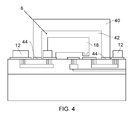
Figure 4 is a schematic side cross section illustrating a further embodiment of the MEMS switch device with a protective cap formed over a portion of the MEMS switch module; -
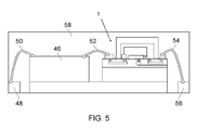
Figure 5 is a schematic side cross section illustrating the MEMS switch device and protective cap shown inFigure 4 packaged in combination with a control module; and -
Figure 6 is a flowchart illustrating a method for manufacturing a MEMS switch device, according to one embodiment. -
Figure 1 schematically illustrates aMEMS switch device 1 according to one embodiment. TheMEMS switch device 1 includes asubstrate layer 2, aninsulating layer 4 formed over thesubstrate layer 2, and aMEMS switch module 6 formed on the surface of theinsulating layer 4. Thesubstrate layer 2 and theinsulating layer 4 can be formed using equipment and materials typically employed for complementary metal-oxide-semiconductor (CMOS) backend processing techniques (e.g., oxide deposition, tungsten deposition, aluminum deposition, photolithography and etching, chemical mechanical planarization, etc.), although other suitable processing techniques may be used. Thesubstrate layer 2 andinsulating layer 4 are referred to together herein as aCMOS backend 8. In the particular embodiment illustrated inFigure 1 , theCMOS backend 8 has a number ofconductive pathways 10 formed within theinsulating layer 4. Theconductive pathways 10 can interconnectselected contacts 12 of theMEMS switch module 6 formed on a surface of theinsulating layer 4. It will be understood that, in practice, theinsulating layer 4 is typically formed from multiple oxide depositions. -
Figure 2 schematically illustrates theMEMS switch module 6 formed on the surface of theinsulating layer 4. InFigure 2 , theconductive pathways 10 illustrated inFigure 1 are not illustrated for the purposes of clarity. As referred to above with reference toFigure 1 , the illustratedMEMS switch module 6 includes a number ofelectrical contacts 12 formed on the surface of theinsulating layer 4. In the illustrated embodiment eachcontact 12 includes afirst layer 14 of electrically conductive material, such as any one of the noble metals, e.g. ruthenium or platinum, formed on the surface of theinsulating layer 4, and a second electricallyconductive layer 16 can be formed over the top of thefirst layer 14. Thesecond layer 16 can be more electrically conductive than thefirst layer 14. The secondconductive layer 16 may be, for example, gold, which is highly conductive and highly resistant to corrosion. Thefirst layer 14 can act to ensure a better electrical and physical contact with the insulatinglayer 4 than would be provided with acontact 12 formed solely of the secondconductive material 16, such as gold. In the embodiment illustrated inFigure 2 , theMEMS switch module 6 also includes aMEMS switch beam 18 that is electrically and physically connected to afurther contact 12a, which is referred to herein as an anchor contact. TheMEMS switch beam 18 can be formed of gold in some embodiments. Theanchor contact 12a serves a dual purpose of physically supporting one end of theswitch beam 18 on the surface of theinsulating layer 4 and also providing an electrical connection to theswitch beam 18 via thecontact 12a. In the particular embodiment illustrated inFigure 2 , theswitch beam 18 is cantilevered fromanchor contact 12a so as to be separated from the surface of theinsulating layer 4. At the end of theswitch beam 18 opposite to theanchor contact 12a, a contact tip 20 is formed on the underside of thebeam 18, the contact tip 20 being coated in a hard conductive material, such as one of the noble metals. The contact tip 20 is located above a further contact pad 22, which may also be formed from a relatively hardwearing conductive material such as a noble metal. The provision of the hardwearing coatings 20, 22 on the contact tip 20 of theswitch beam 18 and the corresponding contact pad 22 on the surface of the insulatinglayer 4 can prevent these surfaces from potentially softening and sticking together at high switching frequencies, which may occur if a softer conductive material, such as gold, were to be used. While not separately called out inFigures 1 and4 , the material choices for theMEMS switch module 6 ofFigure 2 are also applicable to the MEMS switch modules ofFigures 1 and4 . - In operation, a voltage is applied to a
gate electrode 24, which can also be formed from a noble metal, such as ruthenium. Applying the voltage to thegate electrode 24 creates an electrostatic force attracting theswitch beam 18 towards thegate electrode 24. The electrostatic force causes theswitch beam 18 to deform and the beam tip 20 to come into contact with contact pad 22, thus closing an electric circuit between the contact pad 22 andanchor contact 12a. In the particular embodiment illustrated inFigure 2 , a further projection orprotrusion 26 is formed on the underside of theswitch beam 18 between theanchor pad 12a and thegate electrode 24. Theprotrusion 26, also referred to as a "bumper," prevents theswitch beam 18 from collapsing into contact with thegate electrode 24, which may occur through metal fatigue or if an excessive electrostatic force is generated. - The
MEMS switch module 6 is fabricated on theinsulating layer 4 by using surface processing techniques including deposition, masking and etching steps. In the illustrated embodiment, theswitch module 6 does not include any conductive pathways formed on the surface (e.g., exterior surface) of theinsulating layer 4 interconnecting any of thecontacts -
Figure 3 schematically illustrates theCMOS backend 8, including thesubstrate layer 2 and theinsulating layer 4. In some embodiments theinsulating layer 4 is formed from silicon dioxide, but other insulating materials known to be used instead of silicon dioxide may be used as appropriate. Formed within theinsulating layer 4 are a number ofconductive pathways 10. Typically the conductive pathways include alinear trace 30 formed of a resistant material, such as aluminum, formed horizontally within the insulatinglayer 4. The conductive traces 30 can be buried within the insulatinglayer 4. A number ofconductive vias 32 can extend from thetraces 30 to the surface of the insulatinglayer 4. Theconductive vias 32 may be formed from tungsten plugs, or other appropriate conductive material. Thevias 32 may vary in size and number as appropriate. Thevias 32 and traces 30 are formed within the insulatinglayer 4 using known bulk processing techniques, such as those typically used in the production of CMOS devices. The insulatingsubstrate layer 2 is, typically, in preferred embodiments, formed from high resistivity silicon, but may be formed from other high resistivity substances, such as quartz, sapphire, gallium arsenide and glass etc. Other conductive pathways may be formed within the insulatinglayer 4, as required by the desired electrical circuitry for theMEMS switch module 6. An example of such a further conductive pathway is ahigher resistance resistor 34, which in some embodiments is formed from high resistance poly-silicon embedded within the insulatinglayer 4. Such a resistor when formed underneath theswitch beam 18 of theswitch module 6 can serve the purpose of decoupling any undesirable capacitance between theswitch beam 18 and the insulatinglayer 4. - With reference back to
Figure 1 , it can be seen that theconductive vias 32 form electrical interconnections between the contact pads of theMEMS switch module 6 and the conductor traces 30, thus forming the desired conductive pathways between the different elements of theMEMS switch module 6. The conductive pathways of the illustrated embodiment are thus completely buried within the insulatinglayer 4 and thus protected from corrosion and other degradation. - In further embodiments, further protection of the MEMS switch module is provided by the provision of a protective cap. Referring to
Figure 4 , aprotective silicon cap 40 is placed over theswitch beam 18 of theswitch module 6, leaving therelevant contact pads 12 outside theprotective cap 40. Theprotective cap 40 can be formed from a single block of appropriate material, such as silicon, with aninternal cavity 42 etched out. Thecap 40 is bonded to the surface of the insulatinglayer 4 on which theMEMS switch module 6 is formed using appropriate bonding techniques, such as anodic bonding or using an appropriate adhesive, such as the illustratedglass 44. Theprotective cap 40 helps to prevent moisture and other contaminants from interfering with the switch module operation and helps prevent subsequent plastic molding steps from damaging the switch module during the plastic package assembly process. Theprotective cap 40 can also prevent mechanical damage of the MEMS switch module and can prevent particles getting underneath theswitch beam 18. A further benefit of theprotective cap 40 is to provide a controlled environment in which the actual MEMS switch operates. For example, theinterior cavity 42 of thecap 40 may be filled with an inert gas. -
Figure 5 schematically illustrates the MEMS switch device and protective cap shown inFigure 4 packaged in combination with acontrol module 46. Thecontrol module 46 is preferably an application specific integrated circuit (ASIC) and is provided to generate appropriate high voltage (for example, about 80V) switching signals to be applied to the MEMS switch device in response to received logic signals, for example, about 3V. The lower voltage control logic signals are applied to thecontrol module 46 by means of aninput connection 48 and awire bond connection 50 to the control module. Afurther wire bond 52 can connect an output of thecontrol module 46 and one of the contact pads of the MEMS switch device. The output signals from the MEMS switch device can be output via afurther wire bond 54 to anoutput 56 of the package. In some embodiments theinput connection 48,control module 46,MEMS switch device 1 andoutput 56 are encapsulated in a typicalpackaging plastic material 58 in accordance with known packaging techniques. Whilst illustrated with thecontrol module 46 and MEMSswitch device package 1 side-by-side, alternatively theMEMS switch device 1 may be stacked on top of thecontrol module 46, and some or all of the wirebonds can be replaced with other forms of interconnection (e.g., flipchip, through silicon vias, etc.). -
Figure 6 is a flowchart illustrating a method for manufacturing a MEMS switch device, according to one embodiment. In aninitial step 60 of the illustrated embodiment, thesubstrate layer 2 of the CMOS backend is formed using conventional bulk processing/wafer processing techniques. Thenext step 62 is to form the insulatinglayer 4 over thesubstrate 2, with thesubsequent step 64 being to form the conductive pathways in the insulating layer. The skilled artisan will appreciate that, in practice, portions of the insulatinglayer 4 are formed before and after forming the conductive pathways. The initial steps used to form the backend, including the conductive pathways, can all be completed using conventional bulk processing technology. Subsequent to this, the backend wafer is then processed in accordance with surface processing techniques to form, atstep 66, the MEMS switch module on the surface of the insulatinglayer 4. If desired, the protective cap may subsequently be formed over the switch module (at step 68), with the MEMS switch device and control module, if desired, subsequently packaged in accordance with conventional packaging techniques (step 70). Although the method illustrated inFigure 6 has been described in accordance with particular orders or sequences, it should be appreciated that other orders or sequences may be suitable. - The MEMS switch device and method of fabricating the MEMS switch device according to the embodiments disclosed herein buries the conductive pathways (interconnects) in a manufacturable manner, using backend CMOS-type processing. This avoids the problems experienced with MEMS switch devices fabricated solely with surface micro-machine technology in which the interconnects were unburied and therefore were prone to corrosion and leakage currents between interconnects developing due to exposure.
- Furthermore, as explained above, in some embodiments, the
MEMS switch beam 18 can be formed of a highly conductive and corrosion-resistant metal, particularly gold. Using gold for theswitch beam 18 and the secondconductive layer 16 can greatly reduce the amount of losses as compared to switches manufactured using a semiconductor material (e.g., silicon). Without being limited by theory, it is believed that a gold switch is advantageous compared to using a semiconductor switch because, when the gold switch is closed, the switch acts as a substantially loss-less analog device such that the input signal is substantially the same as the output signal (e.g., the gold switch in the closed configuration may act as a gold wire). In some embodiments, the MEMS switches described herein are integrated with high frequency circuits, such as RF arrays. For example, gold switch beams may be used in RF applications at operating frequencies between about 11 GHz and about 100 GHz. For example in some embodiments, the disclosed switch beams may be used in RF applications at operating frequencies of at least about 77 GHz. - In other embodiments, MEMS switches as described herein are used to replace much larger mechanical relays in applications where a smaller profile is desired. For example, in medical applications in which the switch may be used inside the human body, highly reliable and loss-less MEMS switches disclosed herein may be made to be smaller than conventional mechanical relays.
- Accordingly, in various embodiments, as explained herein, it can be advantageous to use a MEMS switch with conductive parts including gold, platinum, and/or ruthenium. However, the use of such metals in conjunction with conventional CMOS fabrication facilities may be undesirable. For example, if a conventional CMOS fabrication facility were used to fabricate both the
CMOS backend 8 and aMEMS switch module 6 that uses agold switch beam 18, gold used to form theswitch beam 18 may contaminate the carefully calibrated CMOS facilities and any future CMOS processes used in the facility. - Accordingly, it can be advantageous to manufacture the
CMOS backend 8 in a first fabrication facility. TheCMOS backend 8 can then be transported to a separate fabrication facility for the manufacture of theMEMS switch module 6, for example, modules that include gold switch beams. The transfer can be conducted prior to dicing or after dicing wafers. The techniques taught herein enable both the use of buried interconnects and the use of exotic materials for the MEMS switch that may be incompatible with the facility (e.g., CMOS fabrication facility) used to create the buried interconnects.
Claims (15)
- A microelectromechanical systems (MEMS) switch device including:a substrate layer;an insulating layer formed over the substrate layer; anda MEMS switch module having a plurality of contacts formed on a surface of the insulating layer, wherein the insulating layer includes a number of conductive pathways formed within the insulating layer, the conductive pathways being configured to interconnect selected contacts of the MEMS switch module.
- A MEMS switch device according to claim 1, wherein at least one of the conductive pathways includes a track of conductive material below the surface of the insulating layer and at least one conductive via extending from the track to the surface of the insulating layer.
- A MEMS switch device according to claim 2, wherein one or more of the following applies:each conductive via is electrically connected to one of the contacts of the MEMS switch module;the track of conductive material comprises aluminum; andthe conductive via comprises tungsten.
- A MEMS switch device according to any preceding claim, wherein at least one of the conductive pathways includes a track of resistive material, the resistive material optionally comprising polysilicon.
- A MEMS switch device according to claim 4, wherein the conductive pathway is configured as a resistive circuit element.
- A MEMS switch device according to claim 5, wherein the MEMS switch module includes a switch beam, wherein the resistive circuit element is formed within the insulating layer and is aligned with the switch beam.
- A MEMS switch device according to any preceding claim, wherein the insulating layer comprises silicon dioxide.
- A MEMS switch device according to any preceding claim, further comprising a control module in electric communication with the MEMS switch module.
- A MEMS switch device according to claim 1, wherein the substrate layer comprises a high resistivity material, the high resistivity material optionally comprising one of silicon, quartz, sapphire, gallium arsenide and glass.
- A MEMS switch device according to any preceding claim, wherein the MEMS switch device further includes a protective housing enclosing the MEMS switch module, the protective housing preferably comprising silicon bonded to the insulating layer.
- A MEMS switch device according to claim 1, the MEMS switch module comprising a MEMS switch beam, the MEMS switch beam comprising gold.
- A method of fabricating a microelectromechanical systems (MEMS) switch device including:forming an insulating layer over a substrate layer;forming a number of conductive pathways within the insulating layer; andsubsequently forming on the surface of the insulating layer a MEMS switch module including a plurality of contacts, whereby selected contacts are configured to be interconnected by the conductive pathways within the insulating layer.
- The method of claim 12 further including:after forming the MEMS switch module, forming a protective cap enclosing the MEMS switch module.
- The method of claim 12 or 13, further including providing a control module arranged to be in electrical communication with the MEMS switch module.
- The method of claim 14, further including encapsulating the MEMS switch device with a protective plastic material.
Applications Claiming Priority (1)
| Application Number | Priority Date | Filing Date | Title |
|---|---|---|---|
| US13/955,866 US9911563B2 (en) | 2013-07-31 | 2013-07-31 | MEMS switch device and method of fabrication |
Publications (3)
| Publication Number | Publication Date |
|---|---|
| EP2833388A2 true EP2833388A2 (en) | 2015-02-04 |
| EP2833388A3 EP2833388A3 (en) | 2015-03-11 |
| EP2833388B1 EP2833388B1 (en) | 2023-12-13 |
Family
ID=51211702
Family Applications (1)
| Application Number | Title | Priority Date | Filing Date |
|---|---|---|---|
| EP14178181.5A Active EP2833388B1 (en) | 2013-07-31 | 2014-07-23 | A MEMS Switch Device and Method of Fabrication |
Country Status (4)
| Country | Link |
|---|---|
| US (1) | US9911563B2 (en) |
| EP (1) | EP2833388B1 (en) |
| CN (1) | CN104347320B (en) |
| TW (1) | TWI643231B (en) |
Cited By (1)
| Publication number | Priority date | Publication date | Assignee | Title |
|---|---|---|---|---|
| WO2019141908A1 (en) * | 2018-01-22 | 2019-07-25 | Tikitin Oy | Packaged microelectronic component and method of manufacturing thereof |
Families Citing this family (8)
| Publication number | Priority date | Publication date | Assignee | Title |
|---|---|---|---|---|
| CN105575734B (en) * | 2015-12-23 | 2018-11-06 | 北京时代民芯科技有限公司 | A kind of RF MEMS Switches and its manufacturing method |
| CN105621351B (en) * | 2015-12-24 | 2017-11-07 | 中国电子科技集团公司第五十五研究所 | A kind of wafer-level encapsulation method of RF mems switches |
| US10529518B2 (en) | 2016-09-19 | 2020-01-07 | Analog Devices Global | Protection schemes for MEMS switch devices |
| US11501928B2 (en) | 2020-03-27 | 2022-11-15 | Menlo Microsystems, Inc. | MEMS device built on substrate with ruthenium based contact surface material |
| US12202723B2 (en) | 2021-05-18 | 2025-01-21 | Analog Devices International Unlimited Company | Microelectromechanical systems (MEMS) switch and related methods |
| CN117396994A (en) | 2021-05-18 | 2024-01-12 | 亚德诺半导体国际无限责任公司 | Active charge discharge method for MEMS switches |
| DE102021212369A1 (en) | 2021-11-03 | 2023-05-04 | Robert Bosch Gesellschaft mit beschränkter Haftung | Relays and method of operating a relay |
| CN117615987A (en) | 2022-03-31 | 2024-02-27 | 京东方科技集团股份有限公司 | Electronic devices and preparation methods |
Family Cites Families (33)
| Publication number | Priority date | Publication date | Assignee | Title |
|---|---|---|---|---|
| US5638946A (en) * | 1996-01-11 | 1997-06-17 | Northeastern University | Micromechanical switch with insulated switch contact |
| US6046659A (en) * | 1998-05-15 | 2000-04-04 | Hughes Electronics Corporation | Design and fabrication of broadband surface-micromachined micro-electro-mechanical switches for microwave and millimeter-wave applications |
| US6384353B1 (en) * | 2000-02-01 | 2002-05-07 | Motorola, Inc. | Micro-electromechanical system device |
| US6621390B2 (en) | 2001-02-28 | 2003-09-16 | Samsung Electronics Co., Ltd. | Electrostatically-actuated capacitive MEMS (micro electro mechanical system) switch |
| AU2002359370A1 (en) | 2001-11-09 | 2003-05-26 | Coventor, Incorporated | Mems device having contact and standoff bumps and related methods |
| US6624003B1 (en) * | 2002-02-06 | 2003-09-23 | Teravicta Technologies, Inc. | Integrated MEMS device and package |
| GB0206509D0 (en) * | 2002-03-20 | 2002-05-01 | Qinetiq Ltd | Micro-Electromechanical systems |
| JP2004006664A (en) | 2002-04-10 | 2004-01-08 | Sanken Electric Co Ltd | Method for manufacturing semiconductor device |
| US6686820B1 (en) * | 2002-07-11 | 2004-02-03 | Intel Corporation | Microelectromechanical (MEMS) switching apparatus |
| US7042308B2 (en) * | 2004-06-29 | 2006-05-09 | Intel Corporation | Mechanism to prevent self-actuation in a microelectromechanical switch |
| US7442570B2 (en) * | 2005-03-18 | 2008-10-28 | Invensence Inc. | Method of fabrication of a AL/GE bonding in a wafer packaging environment and a product produced therefrom |
| CN101228301A (en) | 2005-05-19 | 2008-07-23 | Memc电子材料有限公司 | High resistivity silicon structure and method for making same |
| JP5188673B2 (en) | 2005-06-09 | 2013-04-24 | 株式会社Sumco | Silicon wafer for IGBT and method for manufacturing the same |
| US7321275B2 (en) * | 2005-06-23 | 2008-01-22 | Intel Corporation | Ultra-low voltage capable zipper switch |
| US7968364B2 (en) * | 2005-10-03 | 2011-06-28 | Analog Devices, Inc. | MEMS switch capping and passivation method |
| US7956633B2 (en) * | 2006-03-06 | 2011-06-07 | Formfactor, Inc. | Stacked guard structures |
| JP4265630B2 (en) * | 2006-08-04 | 2009-05-20 | セイコーエプソン株式会社 | MEMS switch, voltage divider circuit, gain adjustment circuit, attenuator, and method of manufacturing MEMS switch |
| KR101084447B1 (en) * | 2006-12-22 | 2011-11-21 | 아나로그 디바이시즈 인코포레이티드 | Switch driving method and device |
| DE102006061386B3 (en) | 2006-12-23 | 2008-06-19 | Atmel Germany Gmbh | Integrated assembly, its use and method of manufacture |
| US7692519B2 (en) * | 2007-12-21 | 2010-04-06 | General Electric Company | MEMS switch with improved standoff voltage control |
| US7615845B1 (en) * | 2008-06-25 | 2009-11-10 | Infineon Technologies Sensonor As | Active shielding of conductors in MEMS devices |
| JP2010056316A (en) | 2008-08-28 | 2010-03-11 | Sumco Corp | Silicon wafer, and method of manufacturing the same |
| US8294539B2 (en) * | 2008-12-18 | 2012-10-23 | Analog Devices, Inc. | Micro-electro-mechanical switch beam construction with minimized beam distortion and method for constructing |
| US20100156577A1 (en) * | 2008-12-22 | 2010-06-24 | General Electric Company | Micro-electromechanical system switch |
| US8445306B2 (en) | 2008-12-24 | 2013-05-21 | International Business Machines Corporation | Hybrid MEMS RF switch and method of fabricating same |
| US8102637B2 (en) * | 2009-07-22 | 2012-01-24 | Analog Devices, Inc. | Control techniques for electrostatic microelectromechanical (MEM) structure |
| US8569091B2 (en) * | 2009-08-27 | 2013-10-29 | International Business Machines Corporation | Integrated circuit switches, design structure and methods of fabricating the same |
| JP2012079889A (en) * | 2010-09-30 | 2012-04-19 | Toshiba Corp | Semiconductor device |
| US8797127B2 (en) | 2010-11-22 | 2014-08-05 | Taiwan Semiconductor Manufacturing Company, Ltd. | MEMS switch with reduced dielectric charging effect |
| WO2013033613A2 (en) | 2011-09-02 | 2013-03-07 | Cavendish Kinetics, Inc | Rf mems isolation, series and shunt dvc, and small mems |
| TWI431732B (en) * | 2011-09-22 | 2014-03-21 | 矽品精密工業股份有限公司 | Semiconductor package and its manufacturing method |
| US10283582B2 (en) * | 2013-02-25 | 2019-05-07 | Analog Devices Global | Microelectronic circuits and integrated circuits including a non-silicon substrate |
| US20150170911A1 (en) | 2013-12-16 | 2015-06-18 | Analog Devices Technology | Silicon substrate suitable for use with an rf component, and an rf component formed on such a silicon substrate |
-
2013
- 2013-07-31 US US13/955,866 patent/US9911563B2/en active Active
-
2014
- 2014-07-23 EP EP14178181.5A patent/EP2833388B1/en active Active
- 2014-07-28 TW TW103125617A patent/TWI643231B/en active
- 2014-07-30 CN CN201410367891.4A patent/CN104347320B/en active Active
Non-Patent Citations (1)
| Title |
|---|
| None |
Cited By (1)
| Publication number | Priority date | Publication date | Assignee | Title |
|---|---|---|---|---|
| WO2019141908A1 (en) * | 2018-01-22 | 2019-07-25 | Tikitin Oy | Packaged microelectronic component and method of manufacturing thereof |
Also Published As
| Publication number | Publication date |
|---|---|
| TW201508801A (en) | 2015-03-01 |
| TWI643231B (en) | 2018-12-01 |
| CN104347320B (en) | 2018-02-13 |
| US9911563B2 (en) | 2018-03-06 |
| CN104347320A (en) | 2015-02-11 |
| EP2833388A3 (en) | 2015-03-11 |
| EP2833388B1 (en) | 2023-12-13 |
| US20150035387A1 (en) | 2015-02-05 |
Similar Documents
| Publication | Publication Date | Title |
|---|---|---|
| US9911563B2 (en) | MEMS switch device and method of fabrication | |
| JP6397913B2 (en) | DVC using MEMS resistance switch and MIM capacitor | |
| US8264307B2 (en) | Dual substrate MEMS plate switch and method of manufacture | |
| US9583294B2 (en) | MEMS swtich with internal conductive path | |
| US8564387B1 (en) | Thermally tolerant anchor configuration for a circular cantilever | |
| US10647569B2 (en) | Methods of manufacture for MEMS switches with reduced switching voltage | |
| KR20080075791A (en) | Power overlay structure and manufacturing method for MEMS devices | |
| US20160214855A1 (en) | Device and method for protecting feol element and beol element | |
| US10964505B2 (en) | Naturally closed MEMs switch for ESD protection | |
| US10494252B2 (en) | MEMS devices and methods of manufacturing the same | |
| KR20160016851A (en) | Micro-electro-mechanical system(mems) structures and design structures | |
| US10748726B2 (en) | Integrated mechanical device with vertical movement | |
| US10475713B2 (en) | Controllable integrated capacitive device | |
| US20190333728A1 (en) | Shielded dual substrate mems plate switch and method of manufacture | |
| US9653392B2 (en) | Metallic device having mobile element in a cavity of the BEOL of an integrated circuit |
Legal Events
| Date | Code | Title | Description |
|---|---|---|---|
| 17P | Request for examination filed |
Effective date: 20140723 |
|
| AK | Designated contracting states |
Kind code of ref document: A2 Designated state(s): AL AT BE BG CH CY CZ DE DK EE ES FI FR GB GR HR HU IE IS IT LI LT LU LV MC MK MT NL NO PL PT RO RS SE SI SK SM TR |
|
| AX | Request for extension of the european patent |
Extension state: BA ME |
|
| PUAI | Public reference made under article 153(3) epc to a published international application that has entered the european phase |
Free format text: ORIGINAL CODE: 0009012 |
|
| PUAL | Search report despatched |
Free format text: ORIGINAL CODE: 0009013 |
|
| AK | Designated contracting states |
Kind code of ref document: A3 Designated state(s): AL AT BE BG CH CY CZ DE DK EE ES FI FR GB GR HR HU IE IS IT LI LT LU LV MC MK MT NL NO PL PT RO RS SE SI SK SM TR |
|
| AX | Request for extension of the european patent |
Extension state: BA ME |
|
| RIC1 | Information provided on ipc code assigned before grant |
Ipc: H01H 59/00 20060101AFI20150130BHEP Ipc: B81C 1/00 20060101ALN20150130BHEP Ipc: H01H 1/00 20060101ALN20150130BHEP |
|
| RAP1 | Party data changed (applicant data changed or rights of an application transferred) |
Owner name: ANALOG DEVICES GLOBAL |
|
| R17P | Request for examination filed (corrected) |
Effective date: 20150911 |
|
| RBV | Designated contracting states (corrected) |
Designated state(s): AL AT BE BG CH CY CZ DE DK EE ES FI FR GB GR HR HU IE IS IT LI LT LU LV MC MK MT NL NO PL PT RO RS SE SI SK SM TR |
|
| 17Q | First examination report despatched |
Effective date: 20160928 |
|
| STAA | Information on the status of an ep patent application or granted ep patent |
Free format text: STATUS: EXAMINATION IS IN PROGRESS |
|
| RAP1 | Party data changed (applicant data changed or rights of an application transferred) |
Owner name: ANALOG DEVICES GLOBAL UNLIMITED COMPANY |
|
| RAP1 | Party data changed (applicant data changed or rights of an application transferred) |
Owner name: ANALOG DEVICES INTERNATIONAL UNLIMITED COMPANY |
|
| GRAP | Despatch of communication of intention to grant a patent |
Free format text: ORIGINAL CODE: EPIDOSNIGR1 |
|
| STAA | Information on the status of an ep patent application or granted ep patent |
Free format text: STATUS: GRANT OF PATENT IS INTENDED |
|
| RIC1 | Information provided on ipc code assigned before grant |
Ipc: H01H 1/00 20060101ALN20230627BHEP Ipc: B81C 1/00 20060101ALN20230627BHEP Ipc: H01H 59/00 20060101AFI20230627BHEP |
|
| INTG | Intention to grant announced |
Effective date: 20230714 |
|
| GRAS | Grant fee paid |
Free format text: ORIGINAL CODE: EPIDOSNIGR3 |
|
| GRAA | (expected) grant |
Free format text: ORIGINAL CODE: 0009210 |
|
| STAA | Information on the status of an ep patent application or granted ep patent |
Free format text: STATUS: THE PATENT HAS BEEN GRANTED |
|
| AK | Designated contracting states |
Kind code of ref document: B1 Designated state(s): AL AT BE BG CH CY CZ DE DK EE ES FI FR GB GR HR HU IE IS IT LI LT LU LV MC MK MT NL NO PL PT RO RS SE SI SK SM TR |
|
| REG | Reference to a national code |
Ref country code: GB Ref legal event code: FG4D |
|
| REG | Reference to a national code |
Ref country code: CH Ref legal event code: EP |
|
| REG | Reference to a national code |
Ref country code: DE Ref legal event code: R096 Ref document number: 602014089082 Country of ref document: DE |
|
| REG | Reference to a national code |
Ref country code: IE Ref legal event code: FG4D |
|
| PG25 | Lapsed in a contracting state [announced via postgrant information from national office to epo] |
Ref country code: GR Free format text: LAPSE BECAUSE OF FAILURE TO SUBMIT A TRANSLATION OF THE DESCRIPTION OR TO PAY THE FEE WITHIN THE PRESCRIBED TIME-LIMIT Effective date: 20240314 |
|
| REG | Reference to a national code |
Ref country code: LT Ref legal event code: MG9D |
|
| PG25 | Lapsed in a contracting state [announced via postgrant information from national office to epo] |
Ref country code: LT Free format text: LAPSE BECAUSE OF FAILURE TO SUBMIT A TRANSLATION OF THE DESCRIPTION OR TO PAY THE FEE WITHIN THE PRESCRIBED TIME-LIMIT Effective date: 20231213 |
|
| REG | Reference to a national code |
Ref country code: NL Ref legal event code: MP Effective date: 20231213 |
|
| PG25 | Lapsed in a contracting state [announced via postgrant information from national office to epo] |
Ref country code: ES Free format text: LAPSE BECAUSE OF FAILURE TO SUBMIT A TRANSLATION OF THE DESCRIPTION OR TO PAY THE FEE WITHIN THE PRESCRIBED TIME-LIMIT Effective date: 20231213 |
|
| PG25 | Lapsed in a contracting state [announced via postgrant information from national office to epo] |
Ref country code: LT Free format text: LAPSE BECAUSE OF FAILURE TO SUBMIT A TRANSLATION OF THE DESCRIPTION OR TO PAY THE FEE WITHIN THE PRESCRIBED TIME-LIMIT Effective date: 20231213 Ref country code: GR Free format text: LAPSE BECAUSE OF FAILURE TO SUBMIT A TRANSLATION OF THE DESCRIPTION OR TO PAY THE FEE WITHIN THE PRESCRIBED TIME-LIMIT Effective date: 20240314 Ref country code: ES Free format text: LAPSE BECAUSE OF FAILURE TO SUBMIT A TRANSLATION OF THE DESCRIPTION OR TO PAY THE FEE WITHIN THE PRESCRIBED TIME-LIMIT Effective date: 20231213 Ref country code: BG Free format text: LAPSE BECAUSE OF FAILURE TO SUBMIT A TRANSLATION OF THE DESCRIPTION OR TO PAY THE FEE WITHIN THE PRESCRIBED TIME-LIMIT Effective date: 20240313 |
|
| REG | Reference to a national code |
Ref country code: AT Ref legal event code: MK05 Ref document number: 1641200 Country of ref document: AT Kind code of ref document: T Effective date: 20231213 |
|
| PG25 | Lapsed in a contracting state [announced via postgrant information from national office to epo] |
Ref country code: NL Free format text: LAPSE BECAUSE OF FAILURE TO SUBMIT A TRANSLATION OF THE DESCRIPTION OR TO PAY THE FEE WITHIN THE PRESCRIBED TIME-LIMIT Effective date: 20231213 |
|
| PG25 | Lapsed in a contracting state [announced via postgrant information from national office to epo] |
Ref country code: SE Free format text: LAPSE BECAUSE OF FAILURE TO SUBMIT A TRANSLATION OF THE DESCRIPTION OR TO PAY THE FEE WITHIN THE PRESCRIBED TIME-LIMIT Effective date: 20231213 Ref country code: RS Free format text: LAPSE BECAUSE OF FAILURE TO SUBMIT A TRANSLATION OF THE DESCRIPTION OR TO PAY THE FEE WITHIN THE PRESCRIBED TIME-LIMIT Effective date: 20231213 Ref country code: NO Free format text: LAPSE BECAUSE OF FAILURE TO SUBMIT A TRANSLATION OF THE DESCRIPTION OR TO PAY THE FEE WITHIN THE PRESCRIBED TIME-LIMIT Effective date: 20240313 Ref country code: NL Free format text: LAPSE BECAUSE OF FAILURE TO SUBMIT A TRANSLATION OF THE DESCRIPTION OR TO PAY THE FEE WITHIN THE PRESCRIBED TIME-LIMIT Effective date: 20231213 Ref country code: LV Free format text: LAPSE BECAUSE OF FAILURE TO SUBMIT A TRANSLATION OF THE DESCRIPTION OR TO PAY THE FEE WITHIN THE PRESCRIBED TIME-LIMIT Effective date: 20231213 Ref country code: HR Free format text: LAPSE BECAUSE OF FAILURE TO SUBMIT A TRANSLATION OF THE DESCRIPTION OR TO PAY THE FEE WITHIN THE PRESCRIBED TIME-LIMIT Effective date: 20231213 |
|
| PG25 | Lapsed in a contracting state [announced via postgrant information from national office to epo] |
Ref country code: IS Free format text: LAPSE BECAUSE OF FAILURE TO SUBMIT A TRANSLATION OF THE DESCRIPTION OR TO PAY THE FEE WITHIN THE PRESCRIBED TIME-LIMIT Effective date: 20240413 |
|
| PG25 | Lapsed in a contracting state [announced via postgrant information from national office to epo] |
Ref country code: AT Free format text: LAPSE BECAUSE OF FAILURE TO SUBMIT A TRANSLATION OF THE DESCRIPTION OR TO PAY THE FEE WITHIN THE PRESCRIBED TIME-LIMIT Effective date: 20231213 Ref country code: CZ Free format text: LAPSE BECAUSE OF FAILURE TO SUBMIT A TRANSLATION OF THE DESCRIPTION OR TO PAY THE FEE WITHIN THE PRESCRIBED TIME-LIMIT Effective date: 20231213 |
|
| PG25 | Lapsed in a contracting state [announced via postgrant information from national office to epo] |
Ref country code: SK Free format text: LAPSE BECAUSE OF FAILURE TO SUBMIT A TRANSLATION OF THE DESCRIPTION OR TO PAY THE FEE WITHIN THE PRESCRIBED TIME-LIMIT Effective date: 20231213 |
|
| PG25 | Lapsed in a contracting state [announced via postgrant information from national office to epo] |
Ref country code: SM Free format text: LAPSE BECAUSE OF FAILURE TO SUBMIT A TRANSLATION OF THE DESCRIPTION OR TO PAY THE FEE WITHIN THE PRESCRIBED TIME-LIMIT Effective date: 20231213 Ref country code: SK Free format text: LAPSE BECAUSE OF FAILURE TO SUBMIT A TRANSLATION OF THE DESCRIPTION OR TO PAY THE FEE WITHIN THE PRESCRIBED TIME-LIMIT Effective date: 20231213 Ref country code: RO Free format text: LAPSE BECAUSE OF FAILURE TO SUBMIT A TRANSLATION OF THE DESCRIPTION OR TO PAY THE FEE WITHIN THE PRESCRIBED TIME-LIMIT Effective date: 20231213 Ref country code: IT Free format text: LAPSE BECAUSE OF FAILURE TO SUBMIT A TRANSLATION OF THE DESCRIPTION OR TO PAY THE FEE WITHIN THE PRESCRIBED TIME-LIMIT Effective date: 20231213 Ref country code: IS Free format text: LAPSE BECAUSE OF FAILURE TO SUBMIT A TRANSLATION OF THE DESCRIPTION OR TO PAY THE FEE WITHIN THE PRESCRIBED TIME-LIMIT Effective date: 20240413 Ref country code: EE Free format text: LAPSE BECAUSE OF FAILURE TO SUBMIT A TRANSLATION OF THE DESCRIPTION OR TO PAY THE FEE WITHIN THE PRESCRIBED TIME-LIMIT Effective date: 20231213 Ref country code: CZ Free format text: LAPSE BECAUSE OF FAILURE TO SUBMIT A TRANSLATION OF THE DESCRIPTION OR TO PAY THE FEE WITHIN THE PRESCRIBED TIME-LIMIT Effective date: 20231213 Ref country code: AT Free format text: LAPSE BECAUSE OF FAILURE TO SUBMIT A TRANSLATION OF THE DESCRIPTION OR TO PAY THE FEE WITHIN THE PRESCRIBED TIME-LIMIT Effective date: 20231213 |
|
| PG25 | Lapsed in a contracting state [announced via postgrant information from national office to epo] |
Ref country code: PL Free format text: LAPSE BECAUSE OF FAILURE TO SUBMIT A TRANSLATION OF THE DESCRIPTION OR TO PAY THE FEE WITHIN THE PRESCRIBED TIME-LIMIT Effective date: 20231213 Ref country code: PT Free format text: LAPSE BECAUSE OF FAILURE TO SUBMIT A TRANSLATION OF THE DESCRIPTION OR TO PAY THE FEE WITHIN THE PRESCRIBED TIME-LIMIT Effective date: 20240415 |
|
| PG25 | Lapsed in a contracting state [announced via postgrant information from national office to epo] |
Ref country code: PT Free format text: LAPSE BECAUSE OF FAILURE TO SUBMIT A TRANSLATION OF THE DESCRIPTION OR TO PAY THE FEE WITHIN THE PRESCRIBED TIME-LIMIT Effective date: 20240415 Ref country code: PL Free format text: LAPSE BECAUSE OF FAILURE TO SUBMIT A TRANSLATION OF THE DESCRIPTION OR TO PAY THE FEE WITHIN THE PRESCRIBED TIME-LIMIT Effective date: 20231213 |
|
| REG | Reference to a national code |
Ref country code: DE Ref legal event code: R097 Ref document number: 602014089082 Country of ref document: DE |
|
| PG25 | Lapsed in a contracting state [announced via postgrant information from national office to epo] |
Ref country code: DK Free format text: LAPSE BECAUSE OF FAILURE TO SUBMIT A TRANSLATION OF THE DESCRIPTION OR TO PAY THE FEE WITHIN THE PRESCRIBED TIME-LIMIT Effective date: 20231213 |
|
| PLBE | No opposition filed within time limit |
Free format text: ORIGINAL CODE: 0009261 |
|
| STAA | Information on the status of an ep patent application or granted ep patent |
Free format text: STATUS: NO OPPOSITION FILED WITHIN TIME LIMIT |
|
| PG25 | Lapsed in a contracting state [announced via postgrant information from national office to epo] |
Ref country code: SI Free format text: LAPSE BECAUSE OF FAILURE TO SUBMIT A TRANSLATION OF THE DESCRIPTION OR TO PAY THE FEE WITHIN THE PRESCRIBED TIME-LIMIT Effective date: 20231213 |
|
| PG25 | Lapsed in a contracting state [announced via postgrant information from national office to epo] |
Ref country code: SI Free format text: LAPSE BECAUSE OF FAILURE TO SUBMIT A TRANSLATION OF THE DESCRIPTION OR TO PAY THE FEE WITHIN THE PRESCRIBED TIME-LIMIT Effective date: 20231213 Ref country code: DK Free format text: LAPSE BECAUSE OF FAILURE TO SUBMIT A TRANSLATION OF THE DESCRIPTION OR TO PAY THE FEE WITHIN THE PRESCRIBED TIME-LIMIT Effective date: 20231213 |
|
| 26N | No opposition filed |
Effective date: 20240916 |
|
| PG25 | Lapsed in a contracting state [announced via postgrant information from national office to epo] |
Ref country code: MC Free format text: LAPSE BECAUSE OF FAILURE TO SUBMIT A TRANSLATION OF THE DESCRIPTION OR TO PAY THE FEE WITHIN THE PRESCRIBED TIME-LIMIT Effective date: 20231213 |
|
| REG | Reference to a national code |
Ref country code: CH Ref legal event code: PL |
|
| PG25 | Lapsed in a contracting state [announced via postgrant information from national office to epo] |
Ref country code: LU Free format text: LAPSE BECAUSE OF NON-PAYMENT OF DUE FEES Effective date: 20240723 |
|
| PG25 | Lapsed in a contracting state [announced via postgrant information from national office to epo] |
Ref country code: LU Free format text: LAPSE BECAUSE OF NON-PAYMENT OF DUE FEES Effective date: 20240723 |
|
| PG25 | Lapsed in a contracting state [announced via postgrant information from national office to epo] |
Ref country code: CH Free format text: LAPSE BECAUSE OF NON-PAYMENT OF DUE FEES Effective date: 20240731 Ref country code: BE Free format text: LAPSE BECAUSE OF NON-PAYMENT OF DUE FEES Effective date: 20240731 |
|
| REG | Reference to a national code |
Ref country code: BE Ref legal event code: MM Effective date: 20240731 |
|
| PGFP | Annual fee paid to national office [announced via postgrant information from national office to epo] |
Ref country code: GB Payment date: 20250619 Year of fee payment: 12 |
|
| PGFP | Annual fee paid to national office [announced via postgrant information from national office to epo] |
Ref country code: FR Payment date: 20250620 Year of fee payment: 12 |
|
| PG25 | Lapsed in a contracting state [announced via postgrant information from national office to epo] |
Ref country code: IE Free format text: LAPSE BECAUSE OF NON-PAYMENT OF DUE FEES Effective date: 20240723 |
|
| PG25 | Lapsed in a contracting state [announced via postgrant information from national office to epo] |
Ref country code: FI Free format text: LAPSE BECAUSE OF FAILURE TO SUBMIT A TRANSLATION OF THE DESCRIPTION OR TO PAY THE FEE WITHIN THE PRESCRIBED TIME-LIMIT Effective date: 20231213 |
|
| PGFP | Annual fee paid to national office [announced via postgrant information from national office to epo] |
Ref country code: DE Payment date: 20250620 Year of fee payment: 12 |
|
| PG25 | Lapsed in a contracting state [announced via postgrant information from national office to epo] |
Ref country code: CY Free format text: LAPSE BECAUSE OF FAILURE TO SUBMIT A TRANSLATION OF THE DESCRIPTION OR TO PAY THE FEE WITHIN THE PRESCRIBED TIME-LIMIT; INVALID AB INITIO Effective date: 20140723 |
|
| PG25 | Lapsed in a contracting state [announced via postgrant information from national office to epo] |
Ref country code: HU Free format text: LAPSE BECAUSE OF FAILURE TO SUBMIT A TRANSLATION OF THE DESCRIPTION OR TO PAY THE FEE WITHIN THE PRESCRIBED TIME-LIMIT; INVALID AB INITIO Effective date: 20140723 |