EP2831649B1 - An optical mechanism with indexing stage with at least one fixed diameter apodized aperture and method of making same - Google Patents
An optical mechanism with indexing stage with at least one fixed diameter apodized aperture and method of making same Download PDFInfo
- Publication number
- EP2831649B1 EP2831649B1 EP13745735.4A EP13745735A EP2831649B1 EP 2831649 B1 EP2831649 B1 EP 2831649B1 EP 13745735 A EP13745735 A EP 13745735A EP 2831649 B1 EP2831649 B1 EP 2831649B1
- Authority
- EP
- European Patent Office
- Prior art keywords
- aperture
- stage
- optical
- apodized
- substrate
- Prior art date
- Legal status (The legal status is an assumption and is not a legal conclusion. Google has not performed a legal analysis and makes no representation as to the accuracy of the status listed.)
- Active
Links
Images




Classifications
-
- G—PHYSICS
- G02—OPTICS
- G02B—OPTICAL ELEMENTS, SYSTEMS OR APPARATUS
- G02B26/00—Optical devices or arrangements for the control of light using movable or deformable optical elements
- G02B26/02—Optical devices or arrangements for the control of light using movable or deformable optical elements for controlling the intensity of light
-
- B—PERFORMING OPERATIONS; TRANSPORTING
- B05—SPRAYING OR ATOMISING IN GENERAL; APPLYING FLUENT MATERIALS TO SURFACES, IN GENERAL
- B05D—PROCESSES FOR APPLYING FLUENT MATERIALS TO SURFACES, IN GENERAL
- B05D5/00—Processes for applying liquids or other fluent materials to surfaces to obtain special surface effects, finishes or structures
- B05D5/06—Processes for applying liquids or other fluent materials to surfaces to obtain special surface effects, finishes or structures to obtain multicolour or other optical effects
-
- B—PERFORMING OPERATIONS; TRANSPORTING
- B29—WORKING OF PLASTICS; WORKING OF SUBSTANCES IN A PLASTIC STATE IN GENERAL
- B29D—PRODUCING PARTICULAR ARTICLES FROM PLASTICS OR FROM SUBSTANCES IN A PLASTIC STATE
- B29D11/00—Producing optical elements, e.g. lenses or prisms
- B29D11/0073—Optical laminates
-
- B—PERFORMING OPERATIONS; TRANSPORTING
- B29—WORKING OF PLASTICS; WORKING OF SUBSTANCES IN A PLASTIC STATE IN GENERAL
- B29D—PRODUCING PARTICULAR ARTICLES FROM PLASTICS OR FROM SUBSTANCES IN A PLASTIC STATE
- B29D11/00—Producing optical elements, e.g. lenses or prisms
- B29D11/00865—Applying coatings; tinting; colouring
-
- G—PHYSICS
- G02—OPTICS
- G02B—OPTICAL ELEMENTS, SYSTEMS OR APPARATUS
- G02B1/00—Optical elements characterised by the material of which they are made; Optical coatings for optical elements
- G02B1/10—Optical coatings produced by application to, or surface treatment of, optical elements
- G02B1/14—Protective coatings, e.g. hard coatings
-
- G—PHYSICS
- G02—OPTICS
- G02B—OPTICAL ELEMENTS, SYSTEMS OR APPARATUS
- G02B27/00—Optical systems or apparatus not provided for by any of the groups G02B1/00 - G02B26/00, G02B30/00
- G02B27/58—Optics for apodization or superresolution; Optical synthetic aperture systems
-
- G—PHYSICS
- G02—OPTICS
- G02B—OPTICAL ELEMENTS, SYSTEMS OR APPARATUS
- G02B5/00—Optical elements other than lenses
- G02B5/005—Diaphragms
-
- G—PHYSICS
- G02—OPTICS
- G02B—OPTICAL ELEMENTS, SYSTEMS OR APPARATUS
- G02B5/00—Optical elements other than lenses
- G02B5/20—Filters
- G02B5/205—Neutral density filters
-
- G—PHYSICS
- G03—PHOTOGRAPHY; CINEMATOGRAPHY; ANALOGOUS TECHNIQUES USING WAVES OTHER THAN OPTICAL WAVES; ELECTROGRAPHY; HOLOGRAPHY
- G03B—APPARATUS OR ARRANGEMENTS FOR TAKING PHOTOGRAPHS OR FOR PROJECTING OR VIEWING THEM; APPARATUS OR ARRANGEMENTS EMPLOYING ANALOGOUS TECHNIQUES USING WAVES OTHER THAN OPTICAL WAVES; ACCESSORIES THEREFOR
- G03B9/00—Exposure-making shutters; Diaphragms
- G03B9/02—Diaphragms
- G03B9/04—Single movable plate with two or more apertures of graded size, e.g. sliding plate or pivoting plate
Definitions
- the present invention relates generally to an optical mechanism with indexing stage with at least one fixed diameter apodized aperture and methods of making same.
- adjustable camera settings have been critical in obtaining correctly exposed pictures. These adjustments include “shutter speed” (adjustable exposure time of the "film”), “film speed” (choice of film sensitivity), and lens aperture (adjustable diaphragm in the lens). In addition to affecting the film exposure, these adjustments also provide other essential benefits. For example, the shutter speed adjustment allows the photographer to freeze in time a fast moving scene. The film speed allows the photographer to get the desired grain in the image. The lens aperture adjustment allows the photographer to get the desired depth of field.
- the electronic shutter control (adjustable integration time of the image sensor) often replaces the mechanical shutter but does not eliminate the need for the lens aperture adjustment which remains an indispensable tool, not only to control the amount of light impinging on the imaging sensor but also to achieve the desired depth of field in the associated image.
- the mechanical iris consists of multiple blades which can be moved with respect to each other so as to form an adjustable pseudo-circular polygonal aperture. The blades are often attached to an inner ring and an outer ring moved relative to each other to adjust the mechanical iris.
- Most film cameras and many digital cameras incorporate a mechanical iris or some other form of lens aperture adjustment (e.g., a rudimentary aperture wheel).
- Cell phone cameras were, originally, not designed as replacements for traditional cameras.
- Cell phone camera modules were supposed to produce acceptable images in dim light conditions without a flash. For this reason, they were fitted with lenses with a large fixed aperture (e.g., f/2.8) to maximize sensitivity at the expense of the depth of field), and relied on the electronic shutter to adjust the exposure level. Consequently these cell phone cameras with no aperture adjustment produce questionable quality images at low-light level due to objectionable shot noise and readout noise and at high-light level due to poor depth of field and reduced sharpness due to lens aberrations.
- a large fixed aperture e.g., f/2.8
- An apodized aperture greatly reduces the detrimental diffraction effects at small aperture sizes (high f numbers such as F/7+) by minimizing sharp edges that cause the diffraction.
- Others have noted advantages to apodized apertures at larger aperture sizes (F2.8 and above).
- Apodized apertures become increasingly advantageous as optical sensor pixel density or number increases and/or pixel size decreases.
- U.S. Patent No. 7,585,122 discloses an electro-mechanical adjustable aperture camera for cell phone applications and the like that is formed of at least two electrodes, and an electrical circuit for applying a voltage to the electrodes in order to create an electric field between the electrodes.
- U.S. Patent No. 7,929,220 discloses an adjustable apodized lens aperture constructed using photochromic material.
- U.S. Patent No. 6,621,616 discloses certain embodiments providing an electrochromic element for a camera that could be used as a shutter, variable light transmittance filter, and iris simultaneously.
- the present invention provides an optical mechanism for a camera having a camera aperture, such as found in cell phones.
- the optical mechanism includes an indexing stage moveable between at least two distinct positions.
- At least a first fixed diameter apodized aperture manufactured according to the method of claim 1 or 3, is mounted on the stage and configured to be aligned with the camera aperture in one of the distinct positions of the indexing stage, and wherein the first fixed diameter apodized aperture is not aligned with the camera aperture in the other of the distinct positions of the indexing stage.
- the optical mechanism may further include an alignment mechanism, such as a linear or rotary actuator, configured to align the stage in each distinct position.
- the stage may be configured for linear or rotary movement between each of the distinct positions.
- the optical element may provide, in a non-limiting example, a resulting F-stop value of the camera of about F2.0 to about F11.0 with the stage the various distinct positions,
- the stage may include at least two, three or four distinct positions for the indexing stage.
- each fixed diameter apodized aperture includes dye diffused into an optical substrate. Further each fixed diameter apodized aperture may include a clear topcoat..
- Another aspect of the present invention provides a method of making a fixed diameter apodized aperture as disclosed in claim 1.
- the method of forming a fixed diameter apodized aperture may provide that the effective diameter of the apodized aperture is determined by the effective diameter of the mask and the level of diffusion of the dye.
- the mask may be a substantially circular mask which is generally centered on the apodized aperture and may be an optical clear coat. Further the mask may form part of the apodized aperture.
- the method of forming a fixed diameter apodized aperture according to the present invention may further include a planarizing step, wherein the planarizing step includes the at least partial removal of the mask, or wherein the planarizing step includes the addition of a planarizing layer.
- the method of forming a fixed diameter apodized aperture according to present invention allows for easy mass production, wherein a plurality of masks are applied to a single optical substrate for simultaneously forming multiple apertures.
- a method of making a fixed diameter apodized aperture according to another aspect of the present invention is disclosed in claim 3.
- the present invention provides an optical mechanism for a camera having a camera aperture, three embodiments of which are schematically illustrated in figures 1-3 described in further detail below.
- the optical mechanism of each embodiment includes an indexing stage 12 moveable between at least two distinct positions. Any number of distinct positions can be incorporated into the stage 12 depending upon the distinct optical properties desired, one of which is provided at each distinct stage position.
- the stage 12 as schematically shown herein can be formed out of optically clear material.
- a non-optically clear material e.g. metal, may form the stage 12, and in such case the distinct positions of the stage 12 that are aligned with the camera aperture may include openings there through and/or the apodized apertures 10 could be formed as insert windows in the stage 12.
- apodized aperture 10 opening sizes resulting in distinct effective aperture openings for the camera aperture, such as allowing the camera to efficiently and effectively move between any desired f/stop range, for example an F/2.0 size and an F711.0 size.
- the apodized apertures 10 of the present invention can be integrated with optics such as magnification lens (e.g., 2X zoom lens) and/or filters (e.g., color filters) to provide further distinct desired properties at each distinct position.
- magnification lens e.g., 2X zoom lens
- filters e.g., color filters
- At least a first or one fixed diameter apodized aperture 10 is mounted on the stage 12 and configured to be selectably aligned with the camera aperture in one of the distinct positions of the indexing stage12.
- a plurality of distinct fixed diameter apodized apertures 10 may be provided in certain embodiments described below.
- the present disclosure illustrates distinct apodized apertures 10 having varied fixed diameters; however it is possible to have distinct apertures 10 with identical fixed diameters with the incorporation of distinct optics.
- two distinct apodized apertures 10 on the stage 12 may have the same effective fixed diameter (e.g., providing for illustrative purposes an effective F/6 opening for the camera aperture) with one including a zoom lens optic (e.g. 4X zoom lens), whereby the two same sized apodized apertures 10 are distinct providing a 4X zoom with effective F/6.0 size and effective F/6.0 size with no optic.
- a zoom lens optic e.g. 4X zoom lens
- the distinct apertures 10 are described herein and believed to be the most efficient for forming a stage 12 according to the present invention, but nothing prevents the operation of the stage 12 according to the present invention if one or more of the distinct apodized apertures 10 is/are repeated on the stage 12.
- the optical mechanism may be more efficient if apodized aperture 10 for the most common setting is repeated at several spaced locations along the stage 12.
- each fixed diameter apodized aperture 10 on stage 12 is selectably not aligned with the camera aperture in selected other of the distinct positions of the indexing stage 12.
- the optical mechanism of the invention generally includes an actuator 16, such as an electric linear or rotary actuator, for moving the stage 12 between each of the distinct positions. It is possible that the optical mechanism can have a manually operated actuator in place of automated electric linear or rotary actuators, however is presumed that in most desired applications of the optical mechanism of the present invention the automated actuator 16 will be desired.
- an actuator 16 such as an electric linear or rotary actuator
- this figure schematically illustrates a two stop indexing stage 12 with a single apodized aperture 10 of fixed opening associated with one effective opening size when aligned with the camera aperture and an open space 14 that is associated with the cameras existing aperture size when the open space 14 is aligned with the camera aperture.
- the open space 14 can be formed as an empty space as shown, provided the stage 12 is formed of optically clear material. If the stage 12 is formed of a non-optically clear material, e.g., a metal substrate, then the open space 14 can be formed as an opening in the stage 12, or as an optically clear window.
- a linear movement mechanism 16 such as a solenoid can index the stage 12 between two positions, one of which provides that the single aperture 10 is aligned with the camera opening and the open space 14 is not for a first effective camera aperture opening, and a second one of which provides that the single aperture 10 is not aligned with the camera opening and the open space 14 is aligned with the camera opening for a second effective camera aperture opening (which is equal to the natural camera opening).
- the stage can include alignment mechanisms 18 associated with mechanical stops, such as spring biased pivoted detent members 20 as shown.
- the alignment mechanisms can assure that the stage 12 is properly positioned relative to the camera for each of the distinct positions of the stage 12.
- Figure 2 schematically illustrates a three stop indexing stage 12 with a pair of apodized apertures 10 of distinct sized fixed openings and an open space 14 that is associated with the cameras existing aperture size. This embodiment shows three positions that allow the effective opening of the camera to range from the natural camera opening through two alternative distinct effective opening sizes.
- the optical element may, for example, provide a resulting F-stop value of the camera of about F/2.0 to about F/4.0 with the stage in the one of the distinct positions, a resulting F-stop value of the camera of about F/4.5 to about F/7.5 with the stage in a second of the distinct positions and an F-stop value of about F/8.0 to about F/11.0 with the camera aperture in the third of the distinct positions.
- the particular effective aperture opening sizes selected for each position may be selected as desired and these representative examples are intended only to demonstrate or suggest the wide versatility of the present invention.
- the representative embodiment of figure 2 includes an automated linear movement mechanism 16, such as a solenoid that can index the stage 12 between positions in which one of the apertures 10 is aligned with the camera opening or the open space 14 is aligned with the camera opening.
- the stage 12 can also include alignment mechanisms 18 associated with mechanical stops, such as spring biased pivoted detent member 20 as shown.
- the stage 12 is shown as a pivoting member mounted on pivot 22 with slot 24 engaging a pin 26 of the actuator 16 whereby the rotary motion of the stage 12 accommodates and is driven by the linear actuator 16.
- Figure 3 schematically illustrates a representative example of a four stop indexing stage 12 with a set of three distinct apodized apertures 10 of distinct sized fixed openings and an open space 14 that is associated with the cameras existing aperture size.
- a rotary movement mechanism 16 such as a rotary motor, can index the stage 12 between positions in which one of the apertures 10 is aligned with the camera opening or the open space 14 is aligned with the camera opening.
- the stage 12 can include alignment mechanisms 18 associated with mechanical stops, such as spring biased pivoted detent member 20 as shown and described above.
- the stage 12 is shown as a rotating member mounted on a hub or pivot 22.
- the illustrated examples show a linear moving stage 12 with linear actuator 16 in figure 1 , a rotary moving stage 12 with a linear actuator 16 in figure 2 and a rotary moving stage 12 with a rotary actuator 16 in figure 3 .
- Any of these designs can include a number of apodized apertures 10.
- the particular movement mechanism 16 and movement of the stage 12 are likely determined by the space limitations in the final device and these are merely representative examples.
- each fixed diameter apodized aperture 10 includes dye diffused into an optical substrate 30. Further each fixed diameter apodized aperture may include a clear topcoat 32 and 36 described below.
- Another aspect of the present invention provides a method of efficiently and effectively making, e.g., mass producing, a fixed diameter apodized aperture 10 as is schematically shown in figures 4A-6 , and possibly including a planarizing step shown in figures 7a and b.
- the method as described further below comprising the steps of: providing an optical substrate 30 for the apodized aperture 10; Depositing a mask 32 on the substrate 30; Depositing a material 34 containing an optical dye onto the substrate 30; and Diffusing the optical dye into the optical substrate 30, wherein the dye will diffuse into the substrate 30 at least partially under the mask 32 when viewed from above the mask 32 and the substrate 30, forming an apodized aperture 10.
- the substrate 30 can be formed of a wide variety of known optical materials in which the selected dye can diffuse.
- a non-exclusive list of materials for the optical substrate 30 includes UV curable (cationic polymerizable, anionic polymerizable, free radical) materials, Thermally curable (thermosets - free radical, condensation polymers, alcohol/amine + isocyanates, etc.) materials, non curable polymers (thermoplastics) - Siloxanes, acrylates, methacrylates, polyurethanes, polyureas, PMMA, polystyrene, cyclic olefin polymer.
- the mask 32 may be formed of a similar listing of materials however the material must be selected to act as a barrier to dye inhibition whether it is based upon permeability of the coating via solubility or diffusion coefficients. In effect the materials suitable for the mask 32 and the substrate 30 are more or less the same list, but with control of cross-link density/flexibility, and associated parameters then one can make the materials more amenable to diffusion for the substrate 30 or less (or effectively non-existent) for the mask 32.
- the method of forming a fixed diameter apodized aperture 10 may provide that the effective diameter of the apodized aperture 10 is determined by the effective diameter of the mask 32 and the level of diffusion of the dye from material 34.
- the mask 32 may be a substantially circular mask 32 which is generally centered on the apodized aperture 10 and may be formed as an optical clear coat. Further the mask 32 may form part of the final apodized aperture 10.
- FIGS. 4a and b schematically illustrate the application of clear hard coat masks 32 onto an optical substrate 30 for forming a series of apodized apertures 10 of distinct opening sizes.
- nine apertures 10 of three distinct sizes are formed on the substrate 30 with a diffusion method according to the present invention.
- Each substrate need not have distinct sizes as it may be more efficient to form each substrate 30 with identical sized apertures 10.
- the clear coat or mask 32 can be deposited via one or more dispensing nozzles which can also be called printing heads.
- the dispensing nozzles for the clear coat 32 may or may not move relative to the substrate 30.
- the system could employ an indexing work piece holder or a conveyor that moves the substrate 30 relative to one or more nozzles.
- print heads forming the dispensing nozzles for the mask 32 may be provided on an XY indexing slide to move over a stationary substrate 30.
- the deposition will control the size of the mask 32.
- the clear coat or mask 32 could also be vapor deposited (or other deposition method) silicon dioxide (glass).
- silicon dioxide glass
- FIGs 5a and b schematically illustrate the application of a dye layer 34 on the clear hard coat masked optical substrate 30 of figures 4a and b.
- the dye layer 34 can be applied by any known process such as spraying, pouring, or other know application techniques.
- a wide variety of known dyes may be employed in the dye containing layer 34.
- any dye or group of dyes that absorb enough light from 425 to 650 nm so as to remove unwanted light. Suitable examples are known to those of ordinary skill in the art and may be references, for example, in "The Sigma-Aldrich Handbook of Stains, Dyes and Indicators, Floyd Green, 1990, Aldrich Chemical Company". This particular known reference has a huge selection of suitable dyes and dye families.
- Figure 6 illustrates the dispersion of the dye of Figures 5a and b into the optical substrate forming the apodized apertures 10.
- the inclusion of the masks 32 allow for formation of the apodized apertures 10 in the substrate.
- the apertures 10 can be cut out of the substrate 30 as would be known in the art using conventional cutting and edge polishing techniques.
- Figure 7a illustrates the apodized apertures 10 of figure 6 further including planarizing step such as grinding and/or lapping effectively removing the hard coat masks 32 from the aperture 10.
- Figure 7b illustrates the apodized apertures 10 of figure 6 further including a planarizing step of adding a planarizing layer 36.
- the planarizing layer 36 would be formed of known acceptable optical material similar to the substrate 30 and mask 32.
- the layer 36 may be applied in any known fashion; such as for example, spin coating.
- the individual apertures 10 may be removed or separated from the residual portions of the substrate 30 (and layer 36 if present) following final surface processing.
- the substrate 30 may be formed of material of stage 12 whereby the apertures 10 are thereby formed directly on stage 12.
- figure 4 could show the formation of three linear actuated stages 12 each stage 12 having four positions and three apertures 12.
- Forming the substrate 30 as the material forming the stage(s) 12 may thus offer manufacturing advantages requiring that the apertures 10 are spaced properly on the substrate 30. Alternatively there may be cost savings associated with mass production of numerous apertures 10 with no spacing restrictions, and which individual apertures 10 are later attached to a distinct stage 12.
- FIGs 8a and 8b schematically illustrates a set up of another dispersion method according to the present invention for forming a series of apodized apertures of distinct opening sizes.
- This alternative "lateral" dispersion method begins with provision of a substantially clear optical substrate 42 forming a central portion of each aperture 10 and a surrounding dye inclusive containing optical substrate 44.
- the suitable substrates material for substrates 42 and 44 and dyes are the same as described above in connection with substrate 30 and the dye in layer 34 discussed above,
- the provision of the substrates as shown in figures 8a and 8b may be through a number of assembly techniques, one of which is to die cut openings in layer 44 and inserts from a layer of material 42 and place the inserts of material 42 in the openings in the material 44. Other acceptable mass production techniques can be implemented.
- the method includes diffusing the optical dye from the dye containing optical substrate 44 into the clear optical substrate 42 forming an apodized aperture 10.
- Figure 8c illustrates the dispersion of the dye of substrate 44 of Figures 8a and b laterally into the optical substrate 42 forming the apodized apertures 10.
- the apertures 10 need only be separated through conventional techniques. Subsequent processing before separation of the apertures 10 (or after) may also be performed such as adding a planarizing layer or adding an optical layer such as a filter, or other processes as desired.
- the present invention further includes a molding or pour casting method of making a fixed diameter apodized aperture shown generally in figures 9a-10d which Includes the initial step of providing an clear optical substrate 52 for the apodized aperture 10 having radially outwardly diverging sides from the top of the clear optical substrate 52 to the bottom thereof.
- the shape may be convex, concave, straight or combinations thereof.
- a flat topped frusto-conical substrate 52 with concave sides is shown in the figures but a wide variety of shapes may be sufficient. For example a drop shape may be effective and may be economically formed.
- Figures 9a and b schematically illustrates a set up of this pour molding or casting method according to the present invention for forming a series of apodized apertures 10 of distinct opening sizes (six apertures of three distinct sizes in this figure purely as a representation).
- the method begins with a substantially clear optical substrate 52 forming a central portion of each aperture 10 having sloped sides (concave, convex, linear or combinations thereof) as noted.
- the substrate 52 may be provided onto a separate base 30 as shown, or may be part of the base 30' in the embodiment described below in connection with figure 10d .
- the materials forming the substrate 52 are the same as described above in connection with substrate 30 or mask 32.
- the casting method of figures 9-10 includes the casting or pour-molding of a dye containing optical substrate 54 for the apodized aperture 10 surrounding the clear diverging side optical substrate 52 for the apodized aperture 10.
- Figures 10a and 10b illustrate the addition of the pour cast dye including optical substrate 54 to the base 30 and substrate 52 of figure 9A and b to form the apodized apertures 10 according to the present invention. Again numerous casting techniques may be used including spin coating or the like. In this method the dye need not be dispersed from layer 54 into 52 thus the materials may be effectively formed as the mask layer 32 described above. The sloping sides of the substrate 52 create the apodized effect in the final aperture 10.
- the apertures 10 need only be separated through conventional techniques. Subsequent processing before separation of the apertures 10 (or after) may also be performed such as adding a planarizing layer or adding an optical layer such as a filter, or other processes as desired such as removal of base 30.
- Figure 10c illustrates the removal of base 30 from the mold formed apodized apertures 10 of figures 10a and b.
- Figure 10d illustrates an embodiment for casting the apodized apertures 10 according to the present invention similer to figures 10a-b in which the substrates 52 are integral with the base 30'. This may be accomplished by molding of the substrate 52 and base 30', or machining or pressing the substrate shape 52 into the base 30'.
- the present invention further includes a co-molding method of making a fixed diameter apodized aperture 10 of the invention.
- This method is illustrated in figures 11a-d and comprising the steps of: Providing an clear optical substrate 62 for the apodized aperture 10, Providing an dye containing optical substrate 64 for the apodized aperture surrounding the clear optical substrate for the apodized aperture; and Simultaneously providing the clear optical substrate 62 and the dye containing optical substrate 64 in a manner allowing for effectively diffusing the optical dye from the dye containing optical substrate 64 into the dear optical substrate 62 forming an apodized aperture 10.
- the co-molding method of forming a fixed diameter apodized aperture 10 provides that the effective diameter of the apodized aperture 10 is determined by the effective diameter of the clear optical substrate and the level of diffusion. Further as shown in this embodiment as with the other methods described above the clear optical substrate 62 is substantially circular and is generally centered on the apodized aperture 10. However note that any desired shape of apodized aperture could be formed in accordance with the present invention, as dictated by the camera aperture and intended operation of the aperture 10.
- the "diffusion" process of the co-molded design of figures 11-a-d can be slightly different than the above as this "diffusion" may be a mixing of the two materials 62 and 64 before they set in the final configuration. Additionally this co-molding may be a casting type mold or through an injection type molding operation.
- FIGS 11a-d illustrate a co-molded technique for making an apodized aperture 10 wherein a clear flowable central substrate 62 is placed onto base 30 with an annular flowable dye containing substrate 64 with an initial definition or space 66 there between as shown in figures 11a and b.
- the space 66 is filled with a mixture of the substrates 64 and 62 to form the apodized aperture as shown in figures 11c and d.
- This co-molding may be accomplished in a variety of methods including use of a pair of moveable print heads which are used for simultaneously dispensing the dye containing optical substrate 64 and the clear optical substrate 62.
- Fast moving print heads may allow for the ring of material 64 to be placed quickly enough to allow for desired mixing.
- a pair of concentric dispensing nozzles may be used for dispensing the dye containing optical substrate and the clear optical substrate.
- the apertures 10 need only be separated through conventional techniques. Subsequent processing before separation of the apertures 10 (or after) may also be performed such as adding a planarizing layer or adding an optical layer such as a filter, or other processes as desired
- Glass molds were assembled using a 500 um plastic gasket between two glass microscope slides.
- the mold was filled with the monomer formulation using a 3 ml syringe to inject about 1ml of monomer formulation.
- the monomer formulation was cured at 120°C for 2 hours and then cooled to room temperature.
- the clear 2" by 3" polymeric film was then separated from the glass slides.
- the Masking Solution was applied as separate droplets on the clear polymeric substrate using a VCA 2500 VE video contact angle system from AST Products. Three sheets were each printed with different droplet sizes (0.3, 0.5, and 0.7 ⁇ L) in 5 rows of 3 droplets.
- the droplets of Masking Solution were cured for 60 min at 100°C.
- the apertures chosen for imaging did not demonstrate apparent image distortion when a 1x1 mm grid was viewed through the aperture using an Olympus SZH10 zoom stereo microscope.
- the settings were 1.5x objective and 2.0x on the zoom.
- Two transfer optics 2.5x and 0.3x in the light path were used to accommodate the 2/3" camera sensor resulting in a field of view of 4.25 mm x 3.5 mm through the camera.
- Images were acquired using an AVT Stingray 145C digital camera mounted (CMount) on an Olympus SZH zoom stereo microscope resulting in a magnification of 45x.
- the sample was held in place with a custom holder with a 5.1 mm aperture to cut out stray light from the sides.
- the microscope iris was set to 6 to get the greatest depth of field view.
- the Olympus microscope and eyepieces were covered with light blocking material from ThorLabs to remove stray light, particularly for the dark acquisition. Dark acquisition was collected by dosing the manual shutter between the light source and the sample on the microscope stage.
- the data was processed using customized IGOR PROTM, available from WaveMetrics routines.
- Widths of the fixed apodized iris' were obtained as follows.
- the intensity Profiles were extracted either horizontally or vertically.
- the dark level was subtracted out of this information and some "boxcar like” averaging (8 pixels) was performed to improve the signal to noise.
- the profiles for the green response of the image sensor were curve fit with a Gaussian function.
- the Gaussian width from the curve fit in Igor is square root of 2 (SQRT(2)), i.e., 1.4142 times the standard deviation. To get a beam waist, the width is divided by 1.4142 and then multiplied by 2.
- Transmission profile of the green response of the image sensor was calculated by taking a reference image of a glass slide instead of a polymer film, a dark image (manual shutter closed) and the sample image (sample in place) for each sample.
- the transmission profile of the green response of the image sensor was calculated using the following formula and the data across the profile of the image (see equation below). The transmission image was calculated and the transmission green profile was extracted along the same coordinates as the green counts profile.
- Transmission Sample Image ⁇ Dark Acquisition / Reference Image ⁇ Dark Image
- Example 1 (2010-FRB-61) represented in figures 12-13
- Image of apodized part is on the left side of the figure with Green counts profile on the right side of figure 12 .
- Droplet Size - 0.3 microliters - Imbibition Time - 2 hours. Beam waist for green response (counts) was 0.88 mm.
- the beam waist was obtained by curve fitting the counts profiles with a Gaussian function in Igor Pro.
- the Gaussian width parameter was converted to a beam waist by multiplying the Gaussian width by 2/SQRT(2). This provided the beam waist in pixels.
- the pixels were converted to mm by using a 1x1 mm calibrated grid and calculating the number of pixels/millimeter (303 pixels/mm in this case). Transmission profile across the part is shown in figure 13 .
Landscapes
- Physics & Mathematics (AREA)
- General Physics & Mathematics (AREA)
- Optics & Photonics (AREA)
- Engineering & Computer Science (AREA)
- Health & Medical Sciences (AREA)
- Manufacturing & Machinery (AREA)
- Ophthalmology & Optometry (AREA)
- Mechanical Engineering (AREA)
- Optical Elements Other Than Lenses (AREA)
- Diaphragms For Cameras (AREA)
Description
- The present invention relates generally to an optical mechanism with indexing stage with at least one fixed diameter apodized aperture and methods of making same.
- Since essentially the advent of photography adjustable camera settings have been critical in obtaining correctly exposed pictures. These adjustments include "shutter speed" (adjustable exposure time of the "film"), "film speed" (choice of film sensitivity), and lens aperture (adjustable diaphragm in the lens). In addition to affecting the film exposure, these adjustments also provide other essential benefits. For example, the shutter speed adjustment allows the photographer to freeze in time a fast moving scene. The film speed allows the photographer to get the desired grain in the image. The lens aperture adjustment allows the photographer to get the desired depth of field.
- In digital cameras, the electronic shutter control (adjustable integration time of the image sensor) often replaces the mechanical shutter but does not eliminate the need for the lens aperture adjustment which remains an indispensable tool, not only to control the amount of light impinging on the imaging sensor but also to achieve the desired depth of field in the associated image.
- One common form of lens aperture adjustment for digital cameras is the mechanical iris diaphragm or mechanical iris. The mechanical iris consists of multiple blades which can be moved with respect to each other so as to form an adjustable pseudo-circular polygonal aperture. The blades are often attached to an inner ring and an outer ring moved relative to each other to adjust the mechanical iris. Most film cameras and many digital cameras incorporate a mechanical iris or some other form of lens aperture adjustment (e.g., a rudimentary aperture wheel).
- However, there are some notable exceptions: disposable film cameras, very-low-cost digital cameras and many cell phones. The main reason for not using a lens aperture adjustment in these areas is cost. For example, an inexpensive mechanical irise design can be a reasonable component of a digital camera costing possibly less than ½ of 1% of retail price of the total camera unit, but this same inexpensive iris component may cost more than 1/3 of the retail price of a disposable camera or more than 1/3 of the cost of a camera module intended for computer or cellular telephone applications. Thus almost all cell phone cameras (also referred to as cell phone camera modules) do not include a lens aperture adjustment.
- Cell phone cameras were, originally, not designed as replacements for traditional cameras. Cell phone camera modules were supposed to produce acceptable images in dim light conditions without a flash. For this reason, they were fitted with lenses with a large fixed aperture (e.g., f/2.8) to maximize sensitivity at the expense of the depth of field), and relied on the electronic shutter to adjust the exposure level. Consequently these cell phone cameras with no aperture adjustment produce questionable quality images at low-light level due to objectionable shot noise and readout noise and at high-light level due to poor depth of field and reduced sharpness due to lens aberrations.
- However due to their enormous popularity (already outselling film and digital cameras), cell phone camera modules are now poised to replace traditional cameras. As a point of reference on popularity, at the end of 2010 there were over 5.3 billion mobile cell phone subscriptions worldwide or over ¾ of the world population, with the Americas listing 880 million subscriptions and Europe listing 740 million subscriptions. Regarding use of cell phone cameras, according to a December 2010 study 52.7% of mobile users in the United States, 57.5% in Europe and 62.9% in Japan used their mobile cellular devices for taking photographs.
- Cell phone camera modules need to approach or match traditional camera image quality at a fraction of the cost of a traditional camera. This issue is further aggravated by price pressure and market demand for a larger number of pixels. As semiconductor technology progresses, image sensors get sharper and pixels get smaller thus requiring a lens with a wider aperture in order to maintain the same sensitivity. This requirement conflicts with the need for a sharper lens (since a wider aperture results in greater lens aberrations) and for an increased depth of field (since a wider aperture results in a reduced depth of field).
- Two solutions that have attempted to improve cell phone camera modules are the optical auto-focus using a "liquid lens" and the "phase-mask" approach using image processing algorithms. In the case of the optical auto-focus using a liquid lens, the depth of field is not increased. Rather, the focus is simply adjusted for a particular distance. In the case of the phase-mask approach, the focus of the lens is in fact degraded. A phase-mask (placed on one of the lens elements) introduces a relatively constant amount of defocus throughout an extended depth of field. The sharpness is then partially restored by digitally using image processing algorithms. Unfortunately, the sharpness restoration algorithms also introduce a significant amount of noise in the image.
- It is clear that none of these solutions really eliminate the need for an inexpensive adjustable lens aperture but there are no suitable technical implementations fulfilling this need for cell phone camera modules. Current mechanical irises are too expensive, too bulky, too fragile, and too power-hungry to satisfy the expected one-billion cell phone camera module market. Mechanical irises also have another serious technical drawback that diffraction through their circular aperture significantly degrades the image sharpness for small aperture settings, e.g., high f numbers such as f/5.6 or higher.
- An apodized aperture greatly reduces the detrimental diffraction effects at small aperture sizes (high f numbers such as F/7+) by minimizing sharp edges that cause the diffraction. Others have noted advantages to apodized apertures at larger aperture sizes (F2.8 and above). Apodized apertures become increasingly advantageous as optical sensor pixel density or number increases and/or pixel size decreases.
- There have been several proposals in the patent literature that attempt to address these deficiencies such as
U.S. Patent No. 7,585,122 , which discloses an electro-mechanical adjustable aperture camera for cell phone applications and the like that is formed of at least two electrodes, and an electrical circuit for applying a voltage to the electrodes in order to create an electric field between the electrodes.U.S. Patent No. 7,929,220 , discloses an adjustable apodized lens aperture constructed using photochromic material.U.S. Patent No. 6,621,616 , discloses certain embodiments providing an electrochromic element for a camera that could be used as a shutter, variable light transmittance filter, and iris simultaneously.U.S. Published Patent Application Serial Number 2010-0134866 , teaches the broad concept of an optical element with an electrochromic apodized aperture having variable light transmittance in response to the amplitude of an applied voltage. The broad electrochromic apodized aperture solutions of the prior art such as particularly disclosed inU.S. Patent No. 6,621,616 and/orU.S. Published Patent Application Serial Number 2010-0134866 may not, due to complexity, be implemented in a manner that is cost effective for efficient large scale manufacturing. - In addition to cost issues there is a need for durability in a cell phone environment as cell phones typically undergo significantly more abuse than conventional digital or film cameras. Thus there is a need for a certain rugged durability in designs intended for cell phone implementation,
- There remains a need for cost effective, durable, rugged mechanism for varying the aperture of cameras, such as found in cell phones It is an object of the present invention to develop optical elements incorporating the ability to provide distinct apodized apertures for a camera aperture, and methods of making the same suitable for efficient, effective manufacturing for incorporation into inexpensive camera units such as cell phones.
- The following documents deal with apodized apertures
JP 2005 062733 US 2005/084774 ,EP 1 537 910 A1JP H06 287537 A WO 2007/075826 A2 andWO 03/009040 A1 - The present invention provides an optical mechanism for a camera having a camera aperture, such as found in cell phones. The optical mechanism includes an indexing stage moveable between at least two distinct positions. At least a first fixed diameter apodized aperture, manufactured according to the method of
claim 1 or 3, is mounted on the stage and configured to be aligned with the camera aperture in one of the distinct positions of the indexing stage, and wherein the first fixed diameter apodized aperture is not aligned with the camera aperture in the other of the distinct positions of the indexing stage. An actuator for moving the stage between each of said distinct positions. - The optical mechanism may further include an alignment mechanism, such as a linear or rotary actuator, configured to align the stage in each distinct position. The stage may be configured for linear or rotary movement between each of the distinct positions. The optical element may provide, in a non-limiting example, a resulting F-stop value of the camera of about F2.0 to about F11.0 with the stage the various distinct positions, In one representative example the stage may include at least two, three or four distinct positions for the indexing stage.
- The optical mechanism according to one non-limiting embodiment of the invention may be provided wherein each fixed diameter apodized aperture includes dye diffused into an optical substrate. Further each fixed diameter apodized aperture may include a clear topcoat..
- Another aspect of the present invention provides a method of making a fixed diameter apodized aperture as disclosed in
claim 1. - In accordance with one aspect of the invention, the method of forming a fixed diameter apodized aperture may provide that the effective diameter of the apodized aperture is determined by the effective diameter of the mask and the level of diffusion of the dye. The mask may be a substantially circular mask which is generally centered on the apodized aperture and may be an optical clear coat. Further the mask may form part of the apodized aperture.
- The method of forming a fixed diameter apodized aperture according to the present invention may further include a planarizing step, wherein the planarizing step includes the at least partial removal of the mask, or wherein the planarizing step includes the addition of a planarizing layer.
- The method of forming a fixed diameter apodized aperture according to present invention allows for easy mass production, wherein a plurality of masks are applied to a single optical substrate for simultaneously forming multiple apertures.
- A method of making a fixed diameter apodized aperture according to another aspect of the present invention is disclosed in claim 3.
- These and other advantages of the present invention will be clarified in the detailed description of the preferred embodiments taken together with the attached figures wherein like reference numerals reference like elements throughout.
-
-
Figure 1 schematically illustrates an optical mechanism formed of a two stop indexing stage with a fixed diameter apodized aperture in accordance with one aspect of the present invention; -
Figure 2 schematically illustrates an optical mechanism formed of a three stop indexing stage with a pair of distinct fixed diameter apodized apertures in accordance with another aspect of the present invention; -
Figure 3 schematically illustrates an optical mechanism formed of a four stop indexing stage with three distinct fixed diameter apodized apertures in accordance with another aspect of the present invention; -
Figure 4a is a schematic top plan view of a series of hard coat masks on an optical substrate for forming a series of apodized apertures of distinct opening sizes with a diffusion method according to one aspect of the present invention; -
Figure 4b is a schematic sectional view of a series of hard coat masks on the optical substrate offigure 4a ; -
Figure 5a is a schematic top plan view of a dye applied to the optical substrate having the series of hard coat masks offigures 4a and b during the diffusion forming of a series of apodized apertures of distinct opening sizes according to one aspect of the present invention; -
Figure 5b is a schematic sectional view of the dye applied to the optical substrate having the series of hard coat masks offigure 5a ; -
Figure 6 is a schematic sectional view of the diffused dye within the optical substrate having the series of hard coat masks following the dye application offigures 5a and 5b ; -
Figures 7a and b are schematic sectional views of the diffused dye within the optical substrate offigure 6 following distinct planarizing options; -
Figure 8a is a schematic top plan view of an initial optical substrate configuration for forming a series of apodized apertures of distinct opening sizes with a diffusion method according to another aspect of the present invention; -
Figure 8b is a schematic sectional view of initial optical substrate configuration for forming a series of apodized apertures offigure 8a ; -
Figure 8c is a schematic sectional view of the diffused dye within the optical substrate following the set up offigures 8a and 8b ; -
Figure 9a is a schematic top plan view of an initial optical substrate configuration for forming a series of apodized apertures of distinct opening sizes with a molding method according to another aspect of the present invention; -
Figure 9b is a schematic sectional view of initial optical substrate configuration for forming a series of apodized apertures offigure 9a ; -
Figure 10a is a schematic top plan view of a cast dye on the optical substrate configuration offigures 9A and b; -
Figure 10b is a schematic sectional view of the dye and optical substrate configuration for forming a series of apodized apertures offigure 10a ; -
Figure 10c is a schematic sectional view of the dye and optical substrate configuration for forming a series of apodized apertures offigures 10a and b following a planarizing step; -
Figure 10d is a schematic sectional view of the dye and optical substrate configuration for forming a series of apodized apertures slightly modified from the configuration offigure 10a ; -
Figure 11a is a schematic top plan view of an initial optical substrate configuration for forming an apodized aperture with a co-molding or printing method according to another aspect of the present invention; -
Figure 11b is a schematic sectional view of initial optical substrate configuration for forming an apodized aperture offigure 11a ; -
Figure 11c is a schematic top plan view of the integrated optical substrate configuration for forming an apodized aperture with the co-molding or printing method offigures 11a and b; -
Figure 11d is a schematic sectional view of the integrated optical substrate configuration for forming an apodized aperture offigure 11c ; -
Figure 12 includes an image of an apodized aperture adjacent a green counts profile on the right side of the figure illustrating results of testing of example 1 of the bench tests of the test apodized aperture formed according to the present invention; -
Figure 13 is a transmission profile of the test aperture offigure 12 ; -
Figure 14 includes an image of an apodized aperture adjacent a green counts profile on the right side of the figure illustrating results of testing of example 2 of the bench tests of the test apodized aperture formed according to the present invention; -
Figure 15 is a transmission profile of the test aperture offigure 14 ; -
Figure 16 includes an image of an apodized aperture adjacent a green counts profile on the right side of the figure illustrating results of testing of example 3 of the bench tests of the test apodized aperture formed according to the present invention; -
Figure 17 is a transmission profile of the test aperture offigure 14 ; and -
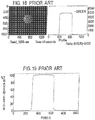
Figures 18 and 19 are illustrations of results of testing a prior art pin hole aperture. - It is noted that, as used in this specification and the appended claims, the singular forms "a," "an," and "the" include plural referents unless expressly and unequivocally limited to one referent. The various embodiments and examples of the present invention as presented herein are each understood to be non-limiting with respect to the scope of the invention.
- The present invention provides an optical mechanism for a camera having a camera aperture, three embodiments of which are schematically illustrated in
figures 1-3 described in further detail below. The optical mechanism of each embodiment includes anindexing stage 12 moveable between at least two distinct positions. Any number of distinct positions can be incorporated into thestage 12 depending upon the distinct optical properties desired, one of which is provided at each distinct stage position. Thestage 12 as schematically shown herein can be formed out of optically clear material. Alternatively, a non-optically clear material, e.g. metal, may form thestage 12, and in such case the distinct positions of thestage 12 that are aligned with the camera aperture may include openings there through and/or theapodized apertures 10 could be formed as insert windows in thestage 12. - The present description is primarily discussing
distinct apodized aperture 10 opening sizes resulting in distinct effective aperture openings for the camera aperture, such as allowing the camera to efficiently and effectively move between any desired f/stop range, for example an F/2.0 size and an F711.0 size. However theapodized apertures 10 of the present invention can be integrated with optics such as magnification lens (e.g., 2X zoom lens) and/or filters (e.g., color filters) to provide further distinct desired properties at each distinct position. The formation of lens and or filters, per se, is not discussed further in this description in detail. - At least a first or one fixed
diameter apodized aperture 10 is mounted on thestage 12 and configured to be selectably aligned with the camera aperture in one of the distinct positions of the indexing stage12. A plurality of distinct fixeddiameter apodized apertures 10 may be provided in certain embodiments described below. The present disclosure illustrates distinctapodized apertures 10 having varied fixed diameters; however it is possible to havedistinct apertures 10 with identical fixed diameters with the incorporation of distinct optics. For example, two distinctapodized apertures 10 on thestage 12 may have the same effective fixed diameter (e.g., providing for illustrative purposes an effective F/6 opening for the camera aperture) with one including a zoom lens optic (e.g. 4X zoom lens), whereby the two same sizedapodized apertures 10 are distinct providing a 4X zoom with effective F/6.0 size and effective F/6.0 size with no optic. - Additionally the
distinct apertures 10 are described herein and believed to be the most efficient for forming astage 12 according to the present invention, but nothing prevents the operation of thestage 12 according to the present invention if one or more of the distinctapodized apertures 10 is/are repeated on thestage 12. For example in astage 12 design with a large number of distinct apertures (e.g., 10+) the optical mechanism may be more efficient ifapodized aperture 10 for the most common setting is repeated at several spaced locations along thestage 12. In general it is believed it will be most effective and efficient ifdistinct apertures 10 are only present once on thestage 12 as shown in the following representative examples. - As should be apparent from the following description each fixed
diameter apodized aperture 10 onstage 12 is selectably not aligned with the camera aperture in selected other of the distinct positions of theindexing stage 12. - The optical mechanism of the invention generally includes an
actuator 16, such as an electric linear or rotary actuator, for moving thestage 12 between each of the distinct positions. It is possible that the optical mechanism can have a manually operated actuator in place of automated electric linear or rotary actuators, however is presumed that in most desired applications of the optical mechanism of the present invention theautomated actuator 16 will be desired. - Turning to the example of the optical mechanism of the invention specifically illustrated in
figure 1 , this figure schematically illustrates a twostop indexing stage 12 with asingle apodized aperture 10 of fixed opening associated with one effective opening size when aligned with the camera aperture and anopen space 14 that is associated with the cameras existing aperture size when theopen space 14 is aligned with the camera aperture. Using the open space allows thestage 12 to utilize the natural camera opening as one effective F/stop size for the camera. Theopen space 14 can be formed as an empty space as shown, provided thestage 12 is formed of optically clear material. If thestage 12 is formed of a non-optically clear material, e.g., a metal substrate, then theopen space 14 can be formed as an opening in thestage 12, or as an optically clear window. - In the representative two stop or two
position stage 12 offigure 1 alinear movement mechanism 16, such as a solenoid can index thestage 12 between two positions, one of which provides that thesingle aperture 10 is aligned with the camera opening and theopen space 14 is not for a first effective camera aperture opening, and a second one of which provides that thesingle aperture 10 is not aligned with the camera opening and theopen space 14 is aligned with the camera opening for a second effective camera aperture opening (which is equal to the natural camera opening). - In the optical mechanism of the invention and as schematically shown in
figure 1 the stage can includealignment mechanisms 18 associated with mechanical stops, such as spring biased pivoteddetent members 20 as shown. The alignment mechanisms can assure that thestage 12 is properly positioned relative to the camera for each of the distinct positions of thestage 12. -
Figure 2 schematically illustrates a threestop indexing stage 12 with a pair ofapodized apertures 10 of distinct sized fixed openings and anopen space 14 that is associated with the cameras existing aperture size. This embodiment shows three positions that allow the effective opening of the camera to range from the natural camera opening through two alternative distinct effective opening sizes. Thus, as illustrated, there are exactly two fixeddiameter apodized apertures 10 mounted on the indexing stage and wherein the optical element may, for example, provide a resulting F-stop value of the camera of about F/2.0 to about F/4.0 with the stage in the one of the distinct positions, a resulting F-stop value of the camera of about F/4.5 to about F/7.5 with the stage in a second of the distinct positions and an F-stop value of about F/8.0 to about F/11.0 with the camera aperture in the third of the distinct positions. The particular effective aperture opening sizes selected for each position may be selected as desired and these representative examples are intended only to demonstrate or suggest the wide versatility of the present invention. - The representative embodiment of
figure 2 includes an automatedlinear movement mechanism 16, such as a solenoid that can index thestage 12 between positions in which one of theapertures 10 is aligned with the camera opening or theopen space 14 is aligned with the camera opening. Thestage 12 can also includealignment mechanisms 18 associated with mechanical stops, such as spring biased pivoteddetent member 20 as shown. Thestage 12 is shown as a pivoting member mounted onpivot 22 withslot 24 engaging apin 26 of theactuator 16 whereby the rotary motion of thestage 12 accommodates and is driven by thelinear actuator 16. -
Figure 3 schematically illustrates a representative example of a fourstop indexing stage 12 with a set of three distinctapodized apertures 10 of distinct sized fixed openings and anopen space 14 that is associated with the cameras existing aperture size. Arotary movement mechanism 16, such as a rotary motor, can index thestage 12 between positions in which one of theapertures 10 is aligned with the camera opening or theopen space 14 is aligned with the camera opening. Thestage 12 can includealignment mechanisms 18 associated with mechanical stops, such as spring biased pivoteddetent member 20 as shown and described above. Thestage 12 is shown as a rotating member mounted on a hub orpivot 22. - The illustrated examples show a linear moving
stage 12 withlinear actuator 16 infigure 1 , arotary moving stage 12 with alinear actuator 16 infigure 2 and arotary moving stage 12 with arotary actuator 16 infigure 3 . Any of these designs can include a number ofapodized apertures 10. Theparticular movement mechanism 16 and movement of thestage 12 are likely determined by the space limitations in the final device and these are merely representative examples. - The optical mechanism according to one non-limiting embodiment of the invention may be provided wherein each fixed
diameter apodized aperture 10 includes dye diffused into anoptical substrate 30. Further each fixed diameter apodized aperture may include aclear topcoat - Another aspect of the present invention provides a method of efficiently and effectively making, e.g., mass producing, a fixed
diameter apodized aperture 10 as is schematically shown infigures 4A-6 , and possibly including a planarizing step shown infigures 7a and b. The method, as described further below comprising the steps of: providing anoptical substrate 30 for theapodized aperture 10; Depositing amask 32 on thesubstrate 30; Depositing a material 34 containing an optical dye onto thesubstrate 30; and Diffusing the optical dye into theoptical substrate 30, wherein the dye will diffuse into thesubstrate 30 at least partially under themask 32 when viewed from above themask 32 and thesubstrate 30, forming anapodized aperture 10. - The
substrate 30 can be formed of a wide variety of known optical materials in which the selected dye can diffuse. A non-exclusive list of materials for theoptical substrate 30 includes UV curable (cationic polymerizable, anionic polymerizable, free radical) materials, Thermally curable (thermosets - free radical, condensation polymers, alcohol/amine + isocyanates, etc.) materials, non curable polymers (thermoplastics) - Siloxanes, acrylates, methacrylates, polyurethanes, polyureas, PMMA, polystyrene, cyclic olefin polymer. Themask 32 may be formed of a similar listing of materials however the material must be selected to act as a barrier to dye inhibition whether it is based upon permeability of the coating via solubility or diffusion coefficients. In effect the materials suitable for themask 32 and thesubstrate 30 are more or less the same list, but with control of cross-link density/flexibility, and associated parameters then one can make the materials more amenable to diffusion for thesubstrate 30 or less (or effectively non-existent) for themask 32. - The method of forming a fixed
diameter apodized aperture 10 may provide that the effective diameter of theapodized aperture 10 is determined by the effective diameter of themask 32 and the level of diffusion of the dye frommaterial 34. In most embodiments themask 32 may be a substantiallycircular mask 32 which is generally centered on theapodized aperture 10 and may be formed as an optical clear coat. Further themask 32 may form part of thefinal apodized aperture 10. - Turning to the figures,
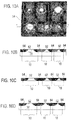
figures 4a and b schematically illustrate the application of clear hard coat masks 32 onto anoptical substrate 30 for forming a series ofapodized apertures 10 of distinct opening sizes. In the schematic illustration nineapertures 10 of three distinct sizes are formed on thesubstrate 30 with a diffusion method according to the present invention. Each substrate need not have distinct sizes as it may be more efficient to form eachsubstrate 30 with identicalsized apertures 10. The clear coat ormask 32 can be deposited via one or more dispensing nozzles which can also be called printing heads. The dispensing nozzles for theclear coat 32 may or may not move relative to thesubstrate 30. For example the system could employ an indexing work piece holder or a conveyor that moves thesubstrate 30 relative to one or more nozzles. Alternatively print heads forming the dispensing nozzles for themask 32 may be provided on an XY indexing slide to move over astationary substrate 30. The deposition will control the size of themask 32. The clear coat ormask 32 could also be vapor deposited (or other deposition method) silicon dioxide (glass). There are numerous effective and cost efficient methods for depositing themasks 32 onto thesubstrate 30, and these are merely representative examples. -
Figures 5a and b schematically illustrate the application of adye layer 34 on the clear hard coat maskedoptical substrate 30 offigures 4a and b. Thedye layer 34 can be applied by any known process such as spraying, pouring, or other know application techniques. A wide variety of known dyes may be employed in thedye containing layer 34. Essentially, any dye or group of dyes that absorb enough light from 425 to 650 nm so as to remove unwanted light. Suitable examples are known to those of ordinary skill in the art and may be references, for example, in "The Sigma-Aldrich Handbook of Stains, Dyes and Indicators, Floyd Green, 1990, Aldrich Chemical Company". This particular known reference has a huge selection of suitable dyes and dye families. - Following depositing of the
layer 34 the system is cured to allow the dispersion or diffusion of the dye in thelayer 34 into thesubstrate 30.Figure 6 illustrates the dispersion of the dye ofFigures 5a and b into the optical substrate forming theapodized apertures 10. As illustrated the inclusion of themasks 32 allow for formation of theapodized apertures 10 in the substrate. At this point theapertures 10 can be cut out of thesubstrate 30 as would be known in the art using conventional cutting and edge polishing techniques. - Prior to separation of the
individual apertures 10 from thesubstrate 30 offigure 6 there may be subsequent surface processing, such as planarizing theapertures 10.Figure 7a illustrates theapodized apertures 10 offigure 6 further including planarizing step such as grinding and/or lapping effectively removing the hard coat masks 32 from theaperture 10. AlternativelyFigure 7b illustrates theapodized apertures 10 offigure 6 further including a planarizing step of adding aplanarizing layer 36. Theplanarizing layer 36 would be formed of known acceptable optical material similar to thesubstrate 30 andmask 32. Thelayer 36 may be applied in any known fashion; such as for example, spin coating. Theindividual apertures 10 may be removed or separated from the residual portions of the substrate 30 (andlayer 36 if present) following final surface processing. - Instead of separating the
apertures 10 into individual components orapertures 10 and attaching these to astage 12, thesubstrate 30 may be formed of material ofstage 12 whereby theapertures 10 are thereby formed directly onstage 12. For example,figure 4 could show the formation of three linear actuated stages 12 eachstage 12 having four positions and threeapertures 12. The threestages 12, following the formation of theapertures 10 thereon, need only be separated andalignment mechanisms 18 added to complete the assembly. Forming thesubstrate 30 as the material forming the stage(s) 12 may thus offer manufacturing advantages requiring that theapertures 10 are spaced properly on thesubstrate 30. Alternatively there may be cost savings associated with mass production ofnumerous apertures 10 with no spacing restrictions, and whichindividual apertures 10 are later attached to adistinct stage 12. -
Figures 8a and 8b schematically illustrates a set up of another dispersion method according to the present invention for forming a series of apodized apertures of distinct opening sizes. This alternative "lateral" dispersion method begins with provision of a substantially clearoptical substrate 42 forming a central portion of eachaperture 10 and a surrounding dye inclusive containingoptical substrate 44. The suitable substrates material forsubstrates substrate 30 and the dye inlayer 34 discussed above, The provision of the substrates as shown infigures 8a and 8b may be through a number of assembly techniques, one of which is to die cut openings inlayer 44 and inserts from a layer ofmaterial 42 and place the inserts ofmaterial 42 in the openings in thematerial 44. Other acceptable mass production techniques can be implemented. - Following the provision of the components (
adjacent layers 42 and 44) of theaperture 10 as shown infigures 8a and b , the method includes diffusing the optical dye from the dye containingoptical substrate 44 into the clearoptical substrate 42 forming anapodized aperture 10.Figure 8c illustrates the dispersion of the dye ofsubstrate 44 ofFigures 8a and b laterally into theoptical substrate 42 forming theapodized apertures 10. Theapertures 10 need only be separated through conventional techniques. Subsequent processing before separation of the apertures 10 (or after) may also be performed such as adding a planarizing layer or adding an optical layer such as a filter, or other processes as desired. - The present invention further includes a molding or pour casting method of making a fixed diameter apodized aperture shown generally in
figures 9a-10d which Includes the initial step of providing an clearoptical substrate 52 for theapodized aperture 10 having radially outwardly diverging sides from the top of the clearoptical substrate 52 to the bottom thereof. The shape may be convex, concave, straight or combinations thereof. A flat topped frusto-conical substrate 52 with concave sides is shown in the figures but a wide variety of shapes may be sufficient. For example a drop shape may be effective and may be economically formed.Figures 9a and b schematically illustrates a set up of this pour molding or casting method according to the present invention for forming a series ofapodized apertures 10 of distinct opening sizes (six apertures of three distinct sizes in this figure purely as a representation). The method begins with a substantially clearoptical substrate 52 forming a central portion of eachaperture 10 having sloped sides (concave, convex, linear or combinations thereof) as noted. Thesubstrate 52 may be provided onto aseparate base 30 as shown, or may be part of the base 30' in the embodiment described below in connection withfigure 10d . The materials forming thesubstrate 52 are the same as described above in connection withsubstrate 30 ormask 32. - The casting method of
figures 9-10 includes the casting or pour-molding of a dye containingoptical substrate 54 for theapodized aperture 10 surrounding the clear diverging sideoptical substrate 52 for theapodized aperture 10.Figures 10a and 10b illustrate the addition of the pour cast dye includingoptical substrate 54 to thebase 30 andsubstrate 52 offigure 9A and b to form theapodized apertures 10 according to the present invention. Again numerous casting techniques may be used including spin coating or the like. In this method the dye need not be dispersed fromlayer 54 into 52 thus the materials may be effectively formed as themask layer 32 described above. The sloping sides of thesubstrate 52 create the apodized effect in thefinal aperture 10. - The
apertures 10 need only be separated through conventional techniques. Subsequent processing before separation of the apertures 10 (or after) may also be performed such as adding a planarizing layer or adding an optical layer such as a filter, or other processes as desired such as removal ofbase 30.Figure 10c illustrates the removal ofbase 30 from the mold formedapodized apertures 10 offigures 10a and b. -
Figure 10d illustrates an embodiment for casting theapodized apertures 10 according to the present invention similer tofigures 10a-b in which thesubstrates 52 are integral with the base 30'. This may be accomplished by molding of thesubstrate 52 and base 30', or machining or pressing thesubstrate shape 52 into the base 30'. - The present invention further includes a co-molding method of making a fixed
diameter apodized aperture 10 of the invention. This method is illustrated infigures 11a-d and comprising the steps of: Providing an clearoptical substrate 62 for theapodized aperture 10, Providing an dye containingoptical substrate 64 for the apodized aperture surrounding the clear optical substrate for the apodized aperture; and Simultaneously providing the clearoptical substrate 62 and the dye containingoptical substrate 64 in a manner allowing for effectively diffusing the optical dye from the dye containingoptical substrate 64 into the dearoptical substrate 62 forming anapodized aperture 10. - As with the processes described above the co-molding method of forming a fixed
diameter apodized aperture 10 provides that the effective diameter of theapodized aperture 10 is determined by the effective diameter of the clear optical substrate and the level of diffusion. Further as shown in this embodiment as with the other methods described above the clearoptical substrate 62 is substantially circular and is generally centered on theapodized aperture 10. However note that any desired shape of apodized aperture could be formed in accordance with the present invention, as dictated by the camera aperture and intended operation of theaperture 10. - The "diffusion" process of the co-molded design of
figures 11-a-d can be slightly different than the above as this "diffusion" may be a mixing of the twomaterials - Specifically for illustration
Figures 11a-d illustrate a co-molded technique for making anapodized aperture 10 wherein a clear flowablecentral substrate 62 is placed ontobase 30 with an annular flowabledye containing substrate 64 with an initial definition orspace 66 there between as shown infigures 11a and b. During setting of thematerials space 66 is filled with a mixture of thesubstrates figures 11c and d. This co-molding may be accomplished in a variety of methods including use of a pair of moveable print heads which are used for simultaneously dispensing the dye containingoptical substrate 64 and the clearoptical substrate 62. Fast moving print heads may allow for the ring ofmaterial 64 to be placed quickly enough to allow for desired mixing. Alternatively a pair of concentric dispensing nozzles may be used for dispensing the dye containing optical substrate and the clear optical substrate. - The
apertures 10 need only be separated through conventional techniques. Subsequent processing before separation of the apertures 10 (or after) may also be performed such as adding a planarizing layer or adding an optical layer such as a filter, or other processes as desired - The following materials were added to a suitable vessel with an agitator: 4.8 g 1-methyl-2-pyrrolidinone; 9.7 g tetrahydrofurfuryl alcohol; 11.4 g diethylene glycol dimethyl ether; 6.5 g propylene glycol butyl ether; 4.0 g hydroxypropylcellulose. These materials were mixed for about 2 hours till the solution was homogenous
- The following materials were added to a suitable vessel with an agitator: 10.0 g Imbibition Resin; 0.30 g Sudan black. The mixture was stirred at 60°C for 60 minutes.
- The following materials were added to a suitable vessel with an agitator;4.0 g BPA 2EO DMA; 6.0 g BPA 30EO DMA; 0.015 g AIBN. The mixture was stirred for 2 hours to dissolve the AIBN. The solution was then degassed under reduced pressure in a vacuum chamber.
- The following materials were added to a suitable vessel with an agitator: 32.4 g Gamma-glycidoxypropyltrimethoxysilane; 345.5 g methyltrimethoxysilane; 292 g deionized water (1 g HNO3 to 7KG water); 228 g 1-methoxy-2-propanol; 0.45 g TMAOH (25% tetramethylammonium hydroxide solution in MeOH); BYK 306 = 2.0 grams. The solution was stirred till homogenous.
- Glass molds were assembled using a 500 um plastic gasket between two glass microscope slides. The mold was filled with the monomer formulation using a 3 ml syringe to inject about 1ml of monomer formulation. The monomer formulation was cured at 120°C for 2 hours and then cooled to room temperature. The clear 2" by 3" polymeric film was then separated from the glass slides. The Masking Solution was applied as separate droplets on the clear polymeric substrate using a VCA 2500 VE video contact angle system from AST Products. Three sheets were each printed with different droplet sizes (0.3, 0.5, and 0.7 µL) in 5 rows of 3 droplets. The droplets of Masking Solution were cured for 60 min at 100°C.
- About 1.5 ml of the Dye Imbibition Resin was applied to the films by spin coating at 1200 RPM for 15 seconds. The coated samples were heated for 60 min at 135°C. The resulting films were washed with soap and water and then the Masking Solution droplets were removed by immersing the films in 10 weight percent NaOH solution with sonication and heating to 60°C. The films were cut into strips (3 apertures per strip) and then the diffusion process was continued for different lengths of time as reported in the examples to vary the diffusion rate and the size of the apodized apertures.
- The apertures chosen for imaging did not demonstrate apparent image distortion when a 1x1 mm grid was viewed through the aperture using an Olympus SZH10 zoom stereo microscope. The settings were 1.5x objective and 2.0x on the zoom. Two transfer optics 2.5x and 0.3x in the light path were used to accommodate the 2/3" camera sensor resulting in a field of view of 4.25 mm x 3.5 mm through the camera.
- Images were acquired using an AVT Stingray 145C digital camera mounted (CMount) on an Olympus SZH zoom stereo microscope resulting in a magnification of 45x. The sample was held in place with a custom holder with a 5.1 mm aperture to cut out stray light from the sides. The microscope iris was set to 6 to get the greatest depth of field view. The camera was set up using AVTs software included with the camera with the following settings: with exposure time = 115 ms (50 microseconds*2300 steps), white balance was fixed, high signal to noise ratio set to ON with 8 images averaged per acquisition - RAW16 format. The Olympus microscope and eyepieces were covered with light blocking material from ThorLabs to remove stray light, particularly for the dark acquisition. Dark acquisition was collected by dosing the manual shutter between the light source and the sample on the microscope stage.
- The data was processed using customized IGOR PRO™, available from WaveMetrics routines.
- Widths of the fixed apodized iris' were obtained as follows. The intensity Profiles were extracted either horizontally or vertically. The dark level was subtracted out of this information and some "boxcar like" averaging (8 pixels) was performed to improve the signal to noise. The profiles for the green response of the image sensor were curve fit with a Gaussian function. The Gaussian width from the curve fit in Igor is square root of 2 (SQRT(2)), i.e., 1.4142 times the standard deviation. To get a beam waist, the width is divided by 1.4142 and then multiplied by 2.
- Transmission profile of the green response of the image sensor was calculated by taking a reference image of a glass slide instead of a polymer film, a dark image (manual shutter closed) and the sample image (sample in place) for each sample. The transmission profile of the green response of the image sensor was calculated using the following formula and the data across the profile of the image (see equation below). The transmission image was calculated and the transmission green profile was extracted along the same coordinates as the green counts profile.

- Image of apodized part is on the left side of the figure with Green counts profile on the right side of
figure 12 . Droplet Size - 0.3 microliters - Imbibition Time - 2 hours. Beam waist for green response (counts) was 0.88 mm. - The beam waist was obtained by curve fitting the counts profiles with a Gaussian function in Igor Pro. The Gaussian width parameter was converted to a beam waist by multiplying the Gaussian width by 2/SQRT(2). This provided the beam waist in pixels. The pixels were converted to mm by using a 1x1 mm calibrated grid and calculating the number of pixels/millimeter (303 pixels/mm in this case). Transmission profile across the part is shown in
figure 13 . - Droplet size - 0.5 microliters. Imbibition time - 8 hours. Beam waist for green response (counts) was 1.21 mm. Transmission profile across the part shown in figure
- Droplet size - 0. 7 microliters, Imbibition time - 8 hours. Beam waist for green response (counts) was 1.21 mm, Transmission profile across the part shown in figure
- Comparative Example of a "normal" non-apodized iris: 1000 micron diameter pinhole aperture (Edmund optics) shown in
figures 18 and 19 . Transmission profile across the part shown infigure 19 . - The present invention has been described with reference to specific details of particular embodiments thereof. It is not intended that such details be regarded as limitations upon the scope of the invention except insofar as and to the extent that they are included in the accompanying claims. The scope of the invention is defined by the appended claims.
Claims (11)
- A method of making a fixed diameter apodized optical aperture (10) comprising the steps of:a. Providing an optical substrate (30) for the apodized aperture (10);b. Depositing a mask (32) on the substrate (30);c. Depositing a material (34) containing an optical dye onto the substrate (30);d. Diffusing the optical dye into the optical substrate (30), wherein the dye will diffuse into the substrate (30) at least partially under the mask (32) when viewed from above the mask (32) and the substrate (30), forming an apodized aperture (10); and optionallye. Planarizing.
- The method of forming a fixed diameter apodized aperture (10) according to claim 1 wherein any one of the following conditions is met:- the effective diameter of the apodized aperture (10) is determined by the effective diameter of the mask (32) and the level of diffusion of step d.,- the mask (32) is a substantially circular mask (32) which is generally centered on the apodized aperture (10),- the mask (32) forms part of the apodized aperture (10),- the mask (32) is a substantially circular optical clear coat,- the planarizing step includes the at least partial removal of the mask (32), or includes the addition of a planarizing layer (36),- a plurality of masks (32) are applied to a single optical substrate (30) for simultaneously forming multiple apertures (10),- the optical substrate (30) is formed from a material selected from the group of UV curable, thermally curable, thermoplastics,- the dye is formed from a material that absorbs light from 325 to 850 nm.
- A method of making a fixed diameter apodized aperture (10) suitable for use in a camera comprising the steps of:a. Providing a clear optical substrate (42) for the apodized aperture (10),b. Providing a dye containing optical substrate (44) for the apodized aperture surrounding the clear optical substrate (42) for the apodized aperture ;c. Diffusing the optical dye from the dye containing optical substrate (44) into the clear optical substrate (42) forming an apodized aperture (10); and optionallyd. Planarizing.
- The method of forming a fixed diameter apodized aperture (10) according to claim 3 wherein any one of the following conditions is met:- the effective diameter of the apodized aperture (10) is determined by the effective diameter of the clear optical substrate (42) and the level of diffusion of step c.,- the diffusing in step c. is conducted by simultaneously providing the clear optical substrate (42) and the dye containing optical substrate (44) in a manner allowing for diffusing the optical dye from the dye containing optical substrate (44) into the clear optical substrate (42) forming an apodized aperture (10), preferably by means of an injection molding operation,- the clear optical substrate (42) is substantially circular and is generally centered on the apodized aperture (10),- multiple apertures (10) are simultaneously formed,- a pair of removable print heads or a pair of concentric dispensing nozzles are used for dispensing the dye containing optical substrate (44) and the clear optical substrate (42).
- An optical mechanism for a camera having a camera aperture, said optical mechanism comprising:a. An indexing stage (12) moveable between at least two distinct positions;b. At least a first fixed diameter apodized aperture (10) made according to a method of any one of claims 1 to 4 mounted on the stage (12) and configured to be aligned with the camera aperture in one of the distinct positions of the indexing stage (12), and wherein the first fixed diameter apodized aperture (10) is not aligned with the camera aperture in the other of the distinct positions of the indexing stage (12);c. An actuator (16) for moving the stage (12) between each of said distinct positions; and optionallyd. An alignment mechanism (18) configured to align the stage (12) in each distinct position.
- The optical mechanism of claim 5, wherein the actuator (16) is a linear actuator (16).
- The optical mechanism of claim 6, wherein the stage (12) is configured for linear movement between each of the distinct positions, optionally including an alignment mechanism (18) configured to align the stage (12) in each of two distinct positions for the indexing stage (12), wherein there is preferably exactly one fixed diameter apodized aperture (10) mounted on the indexing stage (12).
- The optical mechanism of claim 6, wherein the stage (12) is configured for rotary movement between each of the distinct positions, the optical mechanism optionally further including an alignment mechanism (18) configured to align the stage (12) in each of the distinct positions and at least two fixed diameter apodized apertures (10) being mounted on the indexing stage (12), each configured to be aligned with the camera aperture with the indexing stage (12) in selected distinct positions, wherein there are preferably at least three distinct positions for the indexing stage (12).
- The optical mechanism of claim 5, wherein the actuator (16) is a rotary actuator (16) and the stage (12) is configured for rotary movement between each of the distinct positions, the optical mechanism optionally further including an alignment mechanism (18) configured to align the stage (12) in each of the distinct positions and at least two fixed diameter apodized apertures (10) mounted on the indexing stage (12), each being configured to be aligned with the camera aperture with the indexing stage (12) in selected positions, wherein there are preferably at least three distinct positions for the indexing stage (12).
- The optical mechanism of claim 9, including said alignment mechanism (18), wherein there is at least three fixed diameter apodized apertures (10) mounted on the indexing stage (12), each configured to be aligned with the camera aperture with the indexing stage (12) in selected distinct positions, and wherein there are at least three, preferably at least four distinct positions, for the indexing stage (12).
- The optical mechanism of claim 5, wherein each fixed diameter apodized aperture (10) includes a clear topcoat (32, 36).
Applications Claiming Priority (3)
| Application Number | Priority Date | Filing Date | Title |
|---|---|---|---|
| US201261616152P | 2012-03-27 | 2012-03-27 | |
| US13/792,442 US8734033B2 (en) | 2012-03-27 | 2013-03-11 | Optical mechanism with indexing stage with at least one fixed diameter apodized aperture and method of making same |
| PCT/US2013/030449 WO2013148157A2 (en) | 2012-03-27 | 2013-03-12 | An optical mechanism with indexing stage with at least one fixed diameter apodized aperture and method of making same |
Publications (2)
| Publication Number | Publication Date |
|---|---|
| EP2831649A2 EP2831649A2 (en) | 2015-02-04 |
| EP2831649B1 true EP2831649B1 (en) | 2018-05-09 |
Family
ID=49235167
Family Applications (1)
| Application Number | Title | Priority Date | Filing Date |
|---|---|---|---|
| EP13745735.4A Active EP2831649B1 (en) | 2012-03-27 | 2013-03-12 | An optical mechanism with indexing stage with at least one fixed diameter apodized aperture and method of making same |
Country Status (9)
| Country | Link |
|---|---|
| US (1) | US8734033B2 (en) |
| EP (1) | EP2831649B1 (en) |
| JP (2) | JP6159790B2 (en) |
| KR (3) | KR101864610B1 (en) |
| CN (2) | CN104335081A (en) |
| HK (1) | HK1205267A1 (en) |
| MY (1) | MY167345A (en) |
| TW (1) | TWI505016B (en) |
| WO (1) | WO2013148157A2 (en) |
Families Citing this family (16)
| Publication number | Priority date | Publication date | Assignee | Title |
|---|---|---|---|---|
| US8734033B2 (en) * | 2012-03-27 | 2014-05-27 | Ppg Industries Ohio, Inc. | Optical mechanism with indexing stage with at least one fixed diameter apodized aperture and method of making same |
| WO2016063849A1 (en) | 2014-10-21 | 2016-04-28 | 旭硝子株式会社 | Optical element and image pickup device |
| WO2018218063A1 (en) | 2017-05-24 | 2018-11-29 | The Trustees Of Columbia University In The City Of New York | Broadband achromatic flat optical components by dispersion-engineered dielectric metasurfaces |
| JP7461294B2 (en) | 2017-08-31 | 2024-04-03 | メタレンズ,インコーポレイテッド | Transmissive metasurface lens integration |
| JP2021511553A (en) | 2018-01-24 | 2021-05-06 | プレジデント・アンド・フェロウズ・オブ・ハーバード・カレッジ | How to generate a polarized state using a metasurface |
| US12140778B2 (en) | 2018-07-02 | 2024-11-12 | Metalenz, Inc. | Metasurfaces for laser speckle reduction |
| US11978752B2 (en) | 2019-07-26 | 2024-05-07 | Metalenz, Inc. | Aperture-metasurface and hybrid refractive-metasurface imaging systems |
| US11578968B1 (en) | 2019-10-31 | 2023-02-14 | President And Fellows Of Harvard College | Compact metalens depth sensors |
| CN112269268B (en) * | 2020-10-12 | 2022-07-15 | 中国科学院福建物质结构研究所 | Soft-edge diaphragms and coated baffles used in preparation |
| EP4275080A4 (en) | 2021-01-06 | 2024-11-13 | Metalenz, Inc. | Self-aligned nano-pillar coatings and method of manufacturing |
| WO2022251843A1 (en) | 2021-05-25 | 2022-12-01 | Metalenz, Inc. | Single element dot pattern projector |
| US12680877B2 (en) | 2021-07-23 | 2026-07-14 | President And Fellows Of Harvard College | Systems and methods of imaging polarimetry through metasurface polarization gratings |
| CN118591827A (en) | 2021-12-17 | 2024-09-03 | 梅特兰兹股份有限公司 | Anti-spoofing facial recognition via lighting and imaging |
| EP4500265A2 (en) | 2022-03-31 | 2025-02-05 | Metalenz, Inc. | Polarization sorting metasurface microlens array device |
| US12699207B2 (en) | 2022-10-05 | 2026-08-04 | Metalenz, Inc. | Shared-aperture camera system and calibration method |
| CN116803561B (en) * | 2023-08-23 | 2023-10-27 | 太原科技大学 | Board convexity measuring method of quasi-Gaussian distribution |
Citations (5)
| Publication number | Priority date | Publication date | Assignee | Title |
|---|---|---|---|---|
| JPH06287537A (en) * | 1993-02-08 | 1994-10-11 | Fumakilla Ltd | High temperature elapsed time display |
| WO2003009040A1 (en) * | 2001-07-20 | 2003-01-30 | Michel Sayag | Lens system optically coupled to an image-capture device |
| US20050084774A1 (en) * | 2003-08-05 | 2005-04-21 | Canon Kabushiki Kaisha | Production process of light amount-adjusting member, light amount-adjusting member, light amount-adjusting device and photographing apparatus |
| EP1537910A1 (en) * | 2003-12-05 | 2005-06-08 | International Business Machines Corporation | Method and apparatus for forming a chemical gradient on a substrate |
| WO2007075826A2 (en) * | 2005-12-21 | 2007-07-05 | Michel Sayag | Adjustable apodized lens aperture |
Family Cites Families (38)
| Publication number | Priority date | Publication date | Assignee | Title |
|---|---|---|---|---|
| US566270A (en) * | 1896-08-18 | Placket-fastener | ||
| FR2305406A1 (en) * | 1975-03-22 | 1976-10-22 | Hoya Glass Works Ltd | FILTERS FOR LASER PRESENTING A GRADIENT OF TRANSMITTANCE TO THEIR PERIPHERY, GLASS-BASED, AND THEIR PREPARATION PROCESS |
| JPS51109009A (en) * | 1975-03-22 | 1976-09-27 | Hoya Glass Works Ltd | Sofuto apaachua fuirutaanoseizoho |
| US4030817A (en) | 1976-03-22 | 1977-06-21 | The United States Of America As Represented By The Secretary Of The Army | Apodization filter |
| JPS52145052A (en) * | 1976-05-27 | 1977-12-02 | Sumita Optical Glass | Method of making partially colored filter |
| JPS59148035A (en) * | 1983-02-14 | 1984-08-24 | Konishiroku Photo Ind Co Ltd | Exposure controller of camera |
| JP2947577B2 (en) * | 1989-12-15 | 1999-09-13 | 松下電器産業株式会社 | Electronic still camera |
| US5260727A (en) | 1990-10-22 | 1993-11-09 | Oksman Henry C | Wide depth of focus intraocular and contact lenses |
| JPH06317815A (en) * | 1993-04-14 | 1994-11-15 | Fuji Photo Film Co Ltd | Stop plate and film unit with lens using the same |
| US5662706A (en) | 1996-06-14 | 1997-09-02 | Pbh, Inc. | Variable transmissivity annular mask lens for the treatment of optical aberrations |
| US5905561A (en) * | 1996-06-14 | 1999-05-18 | Pbh, Inc. | Annular mask lens having diffraction reducing edges |
| US5965330A (en) | 1996-12-06 | 1999-10-12 | Pbh, Inc. | Methods for fabricating annular mask lens having diffraction-reducing edges |
| US6130448A (en) | 1998-08-21 | 2000-10-10 | Gentex Corporation | Optical sensor package and method of making same |
| US6233403B1 (en) * | 1998-11-04 | 2001-05-15 | Konica Corporation | Lens-fitted film unit with a built-in electronic flash unit and image forming method based on a photographic film exposed by the lens-fitted film unit with a built-in electronic flash unit |
| JP4565711B2 (en) * | 2000-07-26 | 2010-10-20 | リコー光学株式会社 | Manufacturing method of density distribution mask |
| GB0021586D0 (en) * | 2000-09-04 | 2000-10-18 | Lo Tak Sau Anthony | Single lens reflex camera body cap with lens |
| US6433043B1 (en) | 2000-11-28 | 2002-08-13 | Transitions Optical, Inc. | Removable imbibition composition of photochromic compound and kinetic enhancing additive |
| JP2002350954A (en) * | 2001-03-19 | 2002-12-04 | Fuji Photo Film Co Ltd | camera |
| CN100390573C (en) * | 2002-02-19 | 2008-05-28 | 佳能株式会社 | Manufacturing method of light quantity regulating structural element, light quantity regulating structural element, light quantity regulating device and photographic device |
| JP2003241252A (en) * | 2002-02-19 | 2003-08-27 | Canon Inc | Manufacturing method of light amount adjusting member, light amount adjusting member, light amount adjusting device, and photographing device |
| JP2004101956A (en) * | 2002-09-10 | 2004-04-02 | Canon Inc | Optical filter, method for manufacturing optical filter, light amount adjusting device, and photographing device |
| CN100468181C (en) * | 2003-04-30 | 2009-03-11 | 佳能株式会社 | Light amount control apparatus photographing apparatus, and filter |
| JP2004334014A (en) * | 2003-05-09 | 2004-11-25 | Canon Inc | Imaging device |
| JP2005004067A (en) * | 2003-06-13 | 2005-01-06 | Alps Electric Co Ltd | Apodizer |
| JP2005062733A (en) * | 2003-08-20 | 2005-03-10 | Canon Inc | Light amount adjusting device, photographing device, and optical filter |
| US7099555B2 (en) * | 2003-08-20 | 2006-08-29 | Canon Kabushiki Kaisha | Light amount adjusting apparatus, optical equipment, optical filter and image-taking apparatus |
| JP2005215225A (en) * | 2004-01-29 | 2005-08-11 | Canon Inc | Optical filter, optical filter manufacturing method, and vapor deposition mask |
| US7471435B2 (en) * | 2004-02-24 | 2008-12-30 | Modavis Robert A | Apodization technique for enhanced resolution of images |
| US7365917B2 (en) | 2004-08-16 | 2008-04-29 | Xceed Imaging Ltd. | Optical method and system for extended depth of focus |
| US20060038966A1 (en) * | 2004-08-20 | 2006-02-23 | Long Michael D | Apodizing filter |
| US7585122B2 (en) | 2006-03-15 | 2009-09-08 | Nokia Corporation | Aperture construction for a mobile camera |
| JP5058847B2 (en) * | 2007-03-07 | 2012-10-24 | 富士フイルム株式会社 | Optical filter and liquid crystal display device using the same |
| JP5228397B2 (en) * | 2007-04-10 | 2013-07-03 | 住友金属鉱山株式会社 | Heat-resistant light-shielding film, method for producing the same, and diaphragm or light amount adjusting device using the same |
| CN101614833A (en) * | 2008-06-26 | 2009-12-30 | 鸿富锦精密工业(深圳)有限公司 | Lens, lens module and manufacturing method of the lens |
| TW201000942A (en) * | 2008-06-27 | 2010-01-01 | Hon Hai Prec Ind Co Ltd | Lens, lens module and method for manufacturing the lens |
| GB2463480A (en) * | 2008-09-12 | 2010-03-17 | Sharp Kk | Camera Having Large Depth of Field |
| US8373919B2 (en) * | 2008-12-03 | 2013-02-12 | Ppg Industries Ohio, Inc. | Optical element having an apodized aperture |
| US8734033B2 (en) * | 2012-03-27 | 2014-05-27 | Ppg Industries Ohio, Inc. | Optical mechanism with indexing stage with at least one fixed diameter apodized aperture and method of making same |
-
2013
- 2013-03-11 US US13/792,442 patent/US8734033B2/en active Active
- 2013-03-12 MY MYPI2014002532A patent/MY167345A/en unknown
- 2013-03-12 WO PCT/US2013/030449 patent/WO2013148157A2/en not_active Ceased
- 2013-03-12 CN CN201380027960.0A patent/CN104335081A/en active Pending
- 2013-03-12 JP JP2015503255A patent/JP6159790B2/en active Active
- 2013-03-12 EP EP13745735.4A patent/EP2831649B1/en active Active
- 2013-03-12 HK HK15105597.9A patent/HK1205267A1/en unknown
- 2013-03-27 TW TW102111006A patent/TWI505016B/en not_active IP Right Cessation
- 2013-04-03 CN CN201610344360.2A patent/CN106066534B/en active Active
- 2013-04-03 KR KR1020167012027A patent/KR101864610B1/en active Active
- 2013-04-03 KR KR1020177023240A patent/KR20170107026A/en not_active Ceased
- 2013-04-03 KR KR20147030129A patent/KR20150028226A/en not_active Ceased
-
2016
- 2016-04-06 JP JP2016076712A patent/JP6266683B2/en active Active
Patent Citations (5)
| Publication number | Priority date | Publication date | Assignee | Title |
|---|---|---|---|---|
| JPH06287537A (en) * | 1993-02-08 | 1994-10-11 | Fumakilla Ltd | High temperature elapsed time display |
| WO2003009040A1 (en) * | 2001-07-20 | 2003-01-30 | Michel Sayag | Lens system optically coupled to an image-capture device |
| US20050084774A1 (en) * | 2003-08-05 | 2005-04-21 | Canon Kabushiki Kaisha | Production process of light amount-adjusting member, light amount-adjusting member, light amount-adjusting device and photographing apparatus |
| EP1537910A1 (en) * | 2003-12-05 | 2005-06-08 | International Business Machines Corporation | Method and apparatus for forming a chemical gradient on a substrate |
| WO2007075826A2 (en) * | 2005-12-21 | 2007-07-05 | Michel Sayag | Adjustable apodized lens aperture |
Also Published As
| Publication number | Publication date |
|---|---|
| CN104335081A (en) | 2015-02-04 |
| JP2015512529A (en) | 2015-04-27 |
| CN106066534A (en) | 2016-11-02 |
| JP6159790B2 (en) | 2017-07-05 |
| US20130259464A1 (en) | 2013-10-03 |
| US8734033B2 (en) | 2014-05-27 |
| TWI505016B (en) | 2015-10-21 |
| KR20150028226A (en) | 2015-03-13 |
| JP2016164673A (en) | 2016-09-08 |
| MY167345A (en) | 2018-08-16 |
| CN106066534B (en) | 2018-06-01 |
| JP6266683B2 (en) | 2018-01-24 |
| KR20170107026A (en) | 2017-09-22 |
| HK1205267A1 (en) | 2015-12-11 |
| WO2013148157A3 (en) | 2014-02-27 |
| KR101864610B1 (en) | 2018-06-07 |
| EP2831649A2 (en) | 2015-02-04 |
| WO2013148157A2 (en) | 2013-10-03 |
| TW201346424A (en) | 2013-11-16 |
| KR20160058964A (en) | 2016-05-25 |
Similar Documents
| Publication | Publication Date | Title |
|---|---|---|
| US8734033B2 (en) | Optical mechanism with indexing stage with at least one fixed diameter apodized aperture and method of making same | |
| TWI883033B (en) | Optical components and optical devices | |
| TWI439362B (en) | Injection molding micro-optics | |
| CN108474885B (en) | Near-infrared absorbing composition and filter for solid-state imaging device, solid-state imaging device | |
| US20120257292A1 (en) | Wafer Level Lens Module and Method for Manufacturing the Wafer Level Lens Module | |
| US20160011415A1 (en) | Optical lens, method for producing same, lens unit, image-capturing module, and electronic device | |
| US20150103226A1 (en) | Optical lens, lens unit, imaging module, and electronic apparatus | |
| US20180067278A1 (en) | MEMS auto focus miniature camera module with fixed and movable lens groups | |
| EP1892562A1 (en) | Production method for color filter | |
| US20110261252A1 (en) | Imaging system and method of operating the same | |
| CN101846757A (en) | Micro lens and micro lens array | |
| JP2007528515A (en) | Lens array and manufacturing method thereof | |
| WO2015093945A1 (en) | Method of fabricating a wafer level optical lens assembly | |
| TW201700701A (en) | Near-infrared absorbing composition, near-infrared cut filter, method and apparatus for manufacturing near-infrared cut filter, method for producing copper-containing polymer, and copper-containing polymer | |
| US20130293765A1 (en) | MEMS Auto Focus Miniature Camera Module with Abutting Registration | |
| TWI611219B (en) | Method for manufacturing color filter, color filter and solid-state imaging sensing device | |
| US20080166667A1 (en) | Tunable contact angle process for immersionlithography topcoats and photoresists | |
| US20140111875A1 (en) | Method for making paired lenses with an opaque barrier between, and product made | |
| JP6556529B2 (en) | Optical filter and optical device provided with optical filter | |
| US20070127914A1 (en) | Aperture and method for making the same | |
| HK1228514A1 (en) | Method of making a fixed diameter apodized aperture | |
| HK1228514B (en) | Method of making a fixed diameter apodized aperture | |
| US8246795B2 (en) | Lens module fabrication method | |
| CN1614450A (en) | Infrared-ray cut-off filter and its preparation | |
| US20050142467A1 (en) | Color filter manufacturing method, solid state color image sensing apparatus and camera having color filter |
Legal Events
| Date | Code | Title | Description |
|---|---|---|---|
| PUAI | Public reference made under article 153(3) epc to a published international application that has entered the european phase |
Free format text: ORIGINAL CODE: 0009012 |
|
| 17P | Request for examination filed |
Effective date: 20140925 |
|
| AK | Designated contracting states |
Kind code of ref document: A2 Designated state(s): AL AT BE BG CH CY CZ DE DK EE ES FI FR GB GR HR HU IE IS IT LI LT LU LV MC MK MT NL NO PL PT RO RS SE SI SK SM TR |
|
| AX | Request for extension of the european patent |
Extension state: BA ME |
|
| PUAG | Search results despatched under rule 164(2) epc together with communication from examining division |
Free format text: ORIGINAL CODE: 0009017 |
|
| B565 | Issuance of search results under rule 164(2) epc |
Effective date: 20160201 |
|
| STAA | Information on the status of an ep patent application or granted ep patent |
Free format text: STATUS: EXAMINATION IS IN PROGRESS |
|
| GRAP | Despatch of communication of intention to grant a patent |
Free format text: ORIGINAL CODE: EPIDOSNIGR1 |
|
| STAA | Information on the status of an ep patent application or granted ep patent |
Free format text: STATUS: GRANT OF PATENT IS INTENDED |
|
| INTG | Intention to grant announced |
Effective date: 20170706 |
|
| GRAS | Grant fee paid |
Free format text: ORIGINAL CODE: EPIDOSNIGR3 |
|
| GRAJ | Information related to disapproval of communication of intention to grant by the applicant or resumption of examination proceedings by the epo deleted |
Free format text: ORIGINAL CODE: EPIDOSDIGR1 |
|
| GRAL | Information related to payment of fee for publishing/printing deleted |
Free format text: ORIGINAL CODE: EPIDOSDIGR3 |
|
| STAA | Information on the status of an ep patent application or granted ep patent |
Free format text: STATUS: EXAMINATION IS IN PROGRESS |
|
| GRAP | Despatch of communication of intention to grant a patent |
Free format text: ORIGINAL CODE: EPIDOSNIGR1 |
|
| STAA | Information on the status of an ep patent application or granted ep patent |
Free format text: STATUS: GRANT OF PATENT IS INTENDED |
|
| INTC | Intention to grant announced (deleted) | ||
| INTG | Intention to grant announced |
Effective date: 20171205 |
|
| GRAA | (expected) grant |
Free format text: ORIGINAL CODE: 0009210 |
|
| STAA | Information on the status of an ep patent application or granted ep patent |
Free format text: STATUS: THE PATENT HAS BEEN GRANTED |
|
| AK | Designated contracting states |
Kind code of ref document: B1 Designated state(s): AL AT BE BG CH CY CZ DE DK EE ES FI FR GB GR HR HU IE IS IT LI LT LU LV MC MK MT NL NO PL PT RO RS SE SI SK SM TR |
|
| AX | Request for extension of the european patent |
Extension state: BA ME |
|
| REG | Reference to a national code |
Ref country code: GB Ref legal event code: FG4D |
|
| REG | Reference to a national code |
Ref country code: CH Ref legal event code: EP Ref country code: AT Ref legal event code: REF Ref document number: 998077 Country of ref document: AT Kind code of ref document: T Effective date: 20180515 |
|
| REG | Reference to a national code |
Ref country code: IE Ref legal event code: FG4D |
|
| REG | Reference to a national code |
Ref country code: DE Ref legal event code: R096 Ref document number: 602013037235 Country of ref document: DE |
|
| REG | Reference to a national code |
Ref country code: NL Ref legal event code: MP Effective date: 20180509 |
|
| REG | Reference to a national code |
Ref country code: LT Ref legal event code: MG4D |
|
| PG25 | Lapsed in a contracting state [announced via postgrant information from national office to epo] |
Ref country code: BG Free format text: LAPSE BECAUSE OF FAILURE TO SUBMIT A TRANSLATION OF THE DESCRIPTION OR TO PAY THE FEE WITHIN THE PRESCRIBED TIME-LIMIT Effective date: 20180809 Ref country code: NO Free format text: LAPSE BECAUSE OF FAILURE TO SUBMIT A TRANSLATION OF THE DESCRIPTION OR TO PAY THE FEE WITHIN THE PRESCRIBED TIME-LIMIT Effective date: 20180809 Ref country code: LT Free format text: LAPSE BECAUSE OF FAILURE TO SUBMIT A TRANSLATION OF THE DESCRIPTION OR TO PAY THE FEE WITHIN THE PRESCRIBED TIME-LIMIT Effective date: 20180509 Ref country code: ES Free format text: LAPSE BECAUSE OF FAILURE TO SUBMIT A TRANSLATION OF THE DESCRIPTION OR TO PAY THE FEE WITHIN THE PRESCRIBED TIME-LIMIT Effective date: 20180509 Ref country code: SE Free format text: LAPSE BECAUSE OF FAILURE TO SUBMIT A TRANSLATION OF THE DESCRIPTION OR TO PAY THE FEE WITHIN THE PRESCRIBED TIME-LIMIT Effective date: 20180509 Ref country code: FI Free format text: LAPSE BECAUSE OF FAILURE TO SUBMIT A TRANSLATION OF THE DESCRIPTION OR TO PAY THE FEE WITHIN THE PRESCRIBED TIME-LIMIT Effective date: 20180509 |
|
| PG25 | Lapsed in a contracting state [announced via postgrant information from national office to epo] |
Ref country code: LV Free format text: LAPSE BECAUSE OF FAILURE TO SUBMIT A TRANSLATION OF THE DESCRIPTION OR TO PAY THE FEE WITHIN THE PRESCRIBED TIME-LIMIT Effective date: 20180509 Ref country code: NL Free format text: LAPSE BECAUSE OF FAILURE TO SUBMIT A TRANSLATION OF THE DESCRIPTION OR TO PAY THE FEE WITHIN THE PRESCRIBED TIME-LIMIT Effective date: 20180509 Ref country code: GR Free format text: LAPSE BECAUSE OF FAILURE TO SUBMIT A TRANSLATION OF THE DESCRIPTION OR TO PAY THE FEE WITHIN THE PRESCRIBED TIME-LIMIT Effective date: 20180810 Ref country code: RS Free format text: LAPSE BECAUSE OF FAILURE TO SUBMIT A TRANSLATION OF THE DESCRIPTION OR TO PAY THE FEE WITHIN THE PRESCRIBED TIME-LIMIT Effective date: 20180509 Ref country code: HR Free format text: LAPSE BECAUSE OF FAILURE TO SUBMIT A TRANSLATION OF THE DESCRIPTION OR TO PAY THE FEE WITHIN THE PRESCRIBED TIME-LIMIT Effective date: 20180509 |
|
| REG | Reference to a national code |
Ref country code: AT Ref legal event code: MK05 Ref document number: 998077 Country of ref document: AT Kind code of ref document: T Effective date: 20180509 |
|
| PG25 | Lapsed in a contracting state [announced via postgrant information from national office to epo] |
Ref country code: PL Free format text: LAPSE BECAUSE OF FAILURE TO SUBMIT A TRANSLATION OF THE DESCRIPTION OR TO PAY THE FEE WITHIN THE PRESCRIBED TIME-LIMIT Effective date: 20180509 Ref country code: EE Free format text: LAPSE BECAUSE OF FAILURE TO SUBMIT A TRANSLATION OF THE DESCRIPTION OR TO PAY THE FEE WITHIN THE PRESCRIBED TIME-LIMIT Effective date: 20180509 Ref country code: DK Free format text: LAPSE BECAUSE OF FAILURE TO SUBMIT A TRANSLATION OF THE DESCRIPTION OR TO PAY THE FEE WITHIN THE PRESCRIBED TIME-LIMIT Effective date: 20180509 Ref country code: SK Free format text: LAPSE BECAUSE OF FAILURE TO SUBMIT A TRANSLATION OF THE DESCRIPTION OR TO PAY THE FEE WITHIN THE PRESCRIBED TIME-LIMIT Effective date: 20180509 Ref country code: CZ Free format text: LAPSE BECAUSE OF FAILURE TO SUBMIT A TRANSLATION OF THE DESCRIPTION OR TO PAY THE FEE WITHIN THE PRESCRIBED TIME-LIMIT Effective date: 20180509 Ref country code: AT Free format text: LAPSE BECAUSE OF FAILURE TO SUBMIT A TRANSLATION OF THE DESCRIPTION OR TO PAY THE FEE WITHIN THE PRESCRIBED TIME-LIMIT Effective date: 20180509 Ref country code: RO Free format text: LAPSE BECAUSE OF FAILURE TO SUBMIT A TRANSLATION OF THE DESCRIPTION OR TO PAY THE FEE WITHIN THE PRESCRIBED TIME-LIMIT Effective date: 20180509 |
|
| REG | Reference to a national code |
Ref country code: DE Ref legal event code: R097 Ref document number: 602013037235 Country of ref document: DE |
|
| PG25 | Lapsed in a contracting state [announced via postgrant information from national office to epo] |
Ref country code: IT Free format text: LAPSE BECAUSE OF FAILURE TO SUBMIT A TRANSLATION OF THE DESCRIPTION OR TO PAY THE FEE WITHIN THE PRESCRIBED TIME-LIMIT Effective date: 20180509 Ref country code: SM Free format text: LAPSE BECAUSE OF FAILURE TO SUBMIT A TRANSLATION OF THE DESCRIPTION OR TO PAY THE FEE WITHIN THE PRESCRIBED TIME-LIMIT Effective date: 20180509 |
|
| PLBE | No opposition filed within time limit |
Free format text: ORIGINAL CODE: 0009261 |
|
| STAA | Information on the status of an ep patent application or granted ep patent |
Free format text: STATUS: NO OPPOSITION FILED WITHIN TIME LIMIT |
|
| 26N | No opposition filed |
Effective date: 20190212 |
|
| PG25 | Lapsed in a contracting state [announced via postgrant information from national office to epo] |
Ref country code: SI Free format text: LAPSE BECAUSE OF FAILURE TO SUBMIT A TRANSLATION OF THE DESCRIPTION OR TO PAY THE FEE WITHIN THE PRESCRIBED TIME-LIMIT Effective date: 20180509 |
|
| PG25 | Lapsed in a contracting state [announced via postgrant information from national office to epo] |
Ref country code: MC Free format text: LAPSE BECAUSE OF FAILURE TO SUBMIT A TRANSLATION OF THE DESCRIPTION OR TO PAY THE FEE WITHIN THE PRESCRIBED TIME-LIMIT Effective date: 20180509 |
|
| REG | Reference to a national code |
Ref country code: CH Ref legal event code: PL |
|
| PG25 | Lapsed in a contracting state [announced via postgrant information from national office to epo] |
Ref country code: LU Free format text: LAPSE BECAUSE OF NON-PAYMENT OF DUE FEES Effective date: 20190312 Ref country code: AL Free format text: LAPSE BECAUSE OF FAILURE TO SUBMIT A TRANSLATION OF THE DESCRIPTION OR TO PAY THE FEE WITHIN THE PRESCRIBED TIME-LIMIT Effective date: 20180509 |
|
| REG | Reference to a national code |
Ref country code: BE Ref legal event code: MM Effective date: 20190331 |
|
| PG25 | Lapsed in a contracting state [announced via postgrant information from national office to epo] |
Ref country code: CH Free format text: LAPSE BECAUSE OF NON-PAYMENT OF DUE FEES Effective date: 20190331 Ref country code: LI Free format text: LAPSE BECAUSE OF NON-PAYMENT OF DUE FEES Effective date: 20190331 Ref country code: IE Free format text: LAPSE BECAUSE OF NON-PAYMENT OF DUE FEES Effective date: 20190312 |
|
| PG25 | Lapsed in a contracting state [announced via postgrant information from national office to epo] |
Ref country code: BE Free format text: LAPSE BECAUSE OF NON-PAYMENT OF DUE FEES Effective date: 20190331 |
|
| PG25 | Lapsed in a contracting state [announced via postgrant information from national office to epo] |
Ref country code: TR Free format text: LAPSE BECAUSE OF FAILURE TO SUBMIT A TRANSLATION OF THE DESCRIPTION OR TO PAY THE FEE WITHIN THE PRESCRIBED TIME-LIMIT Effective date: 20180509 |
|
| PG25 | Lapsed in a contracting state [announced via postgrant information from national office to epo] |
Ref country code: MT Free format text: LAPSE BECAUSE OF NON-PAYMENT OF DUE FEES Effective date: 20190312 Ref country code: PT Free format text: LAPSE BECAUSE OF FAILURE TO SUBMIT A TRANSLATION OF THE DESCRIPTION OR TO PAY THE FEE WITHIN THE PRESCRIBED TIME-LIMIT Effective date: 20180910 |
|
| PG25 | Lapsed in a contracting state [announced via postgrant information from national office to epo] |
Ref country code: CY Free format text: LAPSE BECAUSE OF FAILURE TO SUBMIT A TRANSLATION OF THE DESCRIPTION OR TO PAY THE FEE WITHIN THE PRESCRIBED TIME-LIMIT Effective date: 20180509 |
|
| PG25 | Lapsed in a contracting state [announced via postgrant information from national office to epo] |
Ref country code: IS Free format text: LAPSE BECAUSE OF FAILURE TO SUBMIT A TRANSLATION OF THE DESCRIPTION OR TO PAY THE FEE WITHIN THE PRESCRIBED TIME-LIMIT Effective date: 20180909 |
|
| PG25 | Lapsed in a contracting state [announced via postgrant information from national office to epo] |
Ref country code: HU Free format text: LAPSE BECAUSE OF FAILURE TO SUBMIT A TRANSLATION OF THE DESCRIPTION OR TO PAY THE FEE WITHIN THE PRESCRIBED TIME-LIMIT; INVALID AB INITIO Effective date: 20130312 |
|
| PG25 | Lapsed in a contracting state [announced via postgrant information from national office to epo] |
Ref country code: MK Free format text: LAPSE BECAUSE OF FAILURE TO SUBMIT A TRANSLATION OF THE DESCRIPTION OR TO PAY THE FEE WITHIN THE PRESCRIBED TIME-LIMIT Effective date: 20180509 |
|
| P01 | Opt-out of the competence of the unified patent court (upc) registered |
Effective date: 20230525 |
|
| P02 | Opt-out of the competence of the unified patent court (upc) changed |
Effective date: 20230529 |
|
| PGFP | Annual fee paid to national office [announced via postgrant information from national office to epo] |
Ref country code: GB Payment date: 20260327 Year of fee payment: 14 |
|
| PGFP | Annual fee paid to national office [announced via postgrant information from national office to epo] |
Ref country code: DE Payment date: 20260327 Year of fee payment: 14 |
|
| PGFP | Annual fee paid to national office [announced via postgrant information from national office to epo] |
Ref country code: FR Payment date: 20260325 Year of fee payment: 14 |