EP2830223A1 - Frequency synthesizer and method of controlling the same - Google Patents
Frequency synthesizer and method of controlling the same Download PDFInfo
- Publication number
- EP2830223A1 EP2830223A1 EP13275259.3A EP13275259A EP2830223A1 EP 2830223 A1 EP2830223 A1 EP 2830223A1 EP 13275259 A EP13275259 A EP 13275259A EP 2830223 A1 EP2830223 A1 EP 2830223A1
- Authority
- EP
- European Patent Office
- Prior art keywords
- frequency
- gain
- gain level
- correction
- phase difference
- Prior art date
- Legal status (The legal status is an assumption and is not a legal conclusion. Google has not performed a legal analysis and makes no representation as to the accuracy of the status listed.)
- Withdrawn
Links
- 238000000034 method Methods 0.000 title claims description 27
- 238000012937 correction Methods 0.000 claims abstract description 103
- 230000003247 decreasing effect Effects 0.000 claims abstract description 7
- 239000003990 capacitor Substances 0.000 claims description 69
- 238000007599 discharging Methods 0.000 claims description 4
- 238000010586 diagram Methods 0.000 description 10
- 238000004088 simulation Methods 0.000 description 3
- 238000004891 communication Methods 0.000 description 1
- 238000005516 engineering process Methods 0.000 description 1
- 238000010295 mobile communication Methods 0.000 description 1
- 238000012986 modification Methods 0.000 description 1
- 230000004048 modification Effects 0.000 description 1
- 238000012545 processing Methods 0.000 description 1
- 230000008054 signal transmission Effects 0.000 description 1
Images




Classifications
-
- H—ELECTRICITY
- H03—ELECTRONIC CIRCUITRY
- H03L—AUTOMATIC CONTROL, STARTING, SYNCHRONISATION OR STABILISATION OF GENERATORS OF ELECTRONIC OSCILLATIONS OR PULSES
- H03L7/00—Automatic control of frequency or phase; Synchronisation
- H03L7/06—Automatic control of frequency or phase; Synchronisation using a reference signal applied to a frequency- or phase-locked loop
- H03L7/08—Details of the phase-locked loop
- H03L7/085—Details of the phase-locked loop concerning mainly the frequency- or phase-detection arrangement including the filtering or amplification of its output signal
- H03L7/087—Details of the phase-locked loop concerning mainly the frequency- or phase-detection arrangement including the filtering or amplification of its output signal using at least two phase detectors or a frequency and phase detector in the loop
-
- H—ELECTRICITY
- H03—ELECTRONIC CIRCUITRY
- H03L—AUTOMATIC CONTROL, STARTING, SYNCHRONISATION OR STABILISATION OF GENERATORS OF ELECTRONIC OSCILLATIONS OR PULSES
- H03L7/00—Automatic control of frequency or phase; Synchronisation
- H03L7/06—Automatic control of frequency or phase; Synchronisation using a reference signal applied to a frequency- or phase-locked loop
- H03L7/08—Details of the phase-locked loop
- H03L7/099—Details of the phase-locked loop concerning mainly the controlled oscillator of the loop
-
- H—ELECTRICITY
- H03—ELECTRONIC CIRCUITRY
- H03L—AUTOMATIC CONTROL, STARTING, SYNCHRONISATION OR STABILISATION OF GENERATORS OF ELECTRONIC OSCILLATIONS OR PULSES
- H03L7/00—Automatic control of frequency or phase; Synchronisation
- H03L7/06—Automatic control of frequency or phase; Synchronisation using a reference signal applied to a frequency- or phase-locked loop
- H03L7/08—Details of the phase-locked loop
- H03L7/085—Details of the phase-locked loop concerning mainly the frequency- or phase-detection arrangement including the filtering or amplification of its output signal
- H03L7/093—Details of the phase-locked loop concerning mainly the frequency- or phase-detection arrangement including the filtering or amplification of its output signal using special filtering or amplification characteristics in the loop
-
- H—ELECTRICITY
- H03—ELECTRONIC CIRCUITRY
- H03L—AUTOMATIC CONTROL, STARTING, SYNCHRONISATION OR STABILISATION OF GENERATORS OF ELECTRONIC OSCILLATIONS OR PULSES
- H03L2207/00—Indexing scheme relating to automatic control of frequency or phase and to synchronisation
- H03L2207/06—Phase locked loops with a controlled oscillator having at least two frequency control terminals
Definitions
- the present invention relates to a frequency synthesizer capable of quickly correcting a deviation in frequency to optimize locking time, and a method of controlling the same.
- a frequency synthesizer is widely used for generating a stable frequency for signal transmission/reception.
- a commonly used frequency synthesizer is a phase-locked loop (PLL) that includes a voltage-controlled oscillator.
- PLL phase-locked loop
- the phase-locked loop may lock an output frequency of the voltage-controlled oscillator in a feedback control manner, and the voltage-controlled oscillator may use a plurality of capacitor banks to determine an output frequency.
- an automatic frequency control scheme has been employed for correcting deviations generated due to an error.
- the auto frequency control scheme requires sequentially searching for frequencies of the capacitor banks in order to set locking due to an error. Therefore, frequency can be correctly locked only after the sequential searching on the capacitor banks is completed, such that locking time for multiple locking is still required.
- Patent Document 1 relates to an AFC control apparatus, an AFC control method, an AFC control program and a mobile communication apparatus, and Patent Document 2 relates to automatic frequency control apparatus and method.
- Patent Document 2 relates to automatic frequency control apparatus and method.
- the inventions disclosed in the Patent Documents require sequential locking if a matching deviation exists in the capacitor banks due to an error on an IC and the like, and thus still have the shortcoming of increased locking times.
- An aspect of the present invention provides a frequency synthesizer and a method of controlling the same capable of determining a deviation in the first locking process, and reflecting the determined deviation in selecting a capacitor bank, thereby eliminating the sequential locking process and reducing the locking time.
- a frequency synthesizer including: a phase-locked loop unit detecting a phase difference between a frequency of a frequency-divided oscillating signal and a frequency of a reference signal so as to adjust dividing of the frequency of the oscillating signal so that the phase difference is decreased within a range of the correction gain levels; an automatic frequency control unit sequentially searching a plurality of frequency gain levels so as to determine a first gain level corresponding to the phase difference between the frequency of the frequency-divided oscillating signal and the frequency of the reference signal; and a correction unit determining a gain correction value using the first gain level so as to determine the correction gain level by reflecting the gain correction value.
- the phase-locked loop unit may include: a phase comparator receiving the oscillating signal and the reference signal so as to output a phase difference between the frequency of the oscillating signal and the frequency of the reference signal; and a voltage-controlled oscillator receiving a control signal corresponding to the phase difference and adjusting the frequency dividing by reflecting the control signal in the correction gain level so as to oscillate the oscillating signal.
- the voltage-controlled oscillator may store a look-up table for a plurality of capacitor banks corresponding to a plurality of frequency gain levels, and may adjust the frequency dividing using a capacitor bank corresponding to the correction gain level.
- the correction unit may determine a difference between the first gain level initially determined in the automatic frequency control unit and the input gain level as the gain correction value, and store it.
- the corrector may determine the correction gain level by reflecting the stored gain correction value if a new input gain level is input.
- the phase-locked loop may include: a charge pump charging or discharging capacitors according to the phase difference output from the phase comparator; and a filter generating the control signal using a current output from the charge pump.
- a frequency synthesizer including: a phase-locked loop detecting a phase difference between a frequency of a frequency-divided oscillating signal and a frequency of a reference signal so as to adjust dividing of the frequency of the oscillating signal so that the phase difference is decreased within a range of the correction gain levels; an automatic frequency control unit searching a plurality of frequency gain levels so as to determine a first gain level corresponding to the phase difference between the frequency of the frequency-divided oscillating signal and the frequency of the reference signal; and a correction unit determining a gain correction value based on the first gain level by a first operation of the automatic frequency control unit, and reflecting the gain correction value after second operation of the automatic frequency control unit.
- the phase-locked loop unit may include: a phase comparator receiving the oscillating signal and the reference signal so as to output a phase difference between the frequency of the oscillating signal and the frequency of the reference signal; and a voltage-controlled oscillator receiving a control signal corresponding to the phase difference and adjusting the frequency dividing by reflecting the control signal in the correction gain level so as to oscillate the oscillating signal.
- the voltage-controlled oscillator may store a look-up table for a plurality of capacitor banks corresponding to a plurality of frequency gain levels, and may adjust the frequency dividing using a capacitor bank corresponding to the correction gain level.
- the correction unit may determine the gain correction value from a difference between a look-up table for the capacitor bank and the first gain level by the first operation.
- the correction unit may determine the correction gain level by reflecting the gain correction value in the look-up table from when the automatic frequency control unit operates for the second time.
- the phase-locked loop may include: a charge pump charging or discharging capacitors according to the phase difference output from the phase comparator; and a filter generating the control signal using a current output from the charge pump.
- a method of controlling a frequency synthesizer using capacitor banks including: determining a phase difference between a frequency of a frequency-divided oscillating signal and a frequency of a reference signal; detecting a first gain level corresponding to the phase difference through automatic frequency control; sequentially searching look-up tables for capacitor banks to determine an input gain level corresponding to the phase difference; and calculating a gain correction value from the difference between the first gain level and the input gain level.
- the detecting of the first gain level may include determining the first gain level using locking information when the automatic frequency control is operated for the first time.
- the method may further include reflecting the gain correction value in the first gain level by the phase difference by the operation from when the automatic frequency control is operated for the second time.
- the method may further include dividing the frequency of the oscillating signal again by reflecting the gain correction value, so as to perform the determining of the phase difference again based on the oscillating signal which was frequency-divided again.
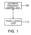
- FIG. 1 is a block diagram for illustrating an example of a frequency synthesizer.
- the frequency synthesizer includes a phase-locked loop unit 110 and an automatic frequency control unit 120.
- the phase-locked loop unit 110 detects a phase difference between a previous oscillating signal and a reference signal, and generates a current oscillating signal by adjusting frequency dividing so that the phase difference is decreased. Here, the generated oscillating signal is fed back to the phase-locked loop unit 110.
- the phase-locked loop unit 110 may use a predetermined gain level to adjust frequency dividing.
- the gain level may be determined based on the information provided from the automatic frequency control unit 120.
- the automatic frequency control unit 120 generates a gain level determining signal to maintain or change the current frequency gain level depending on the difference in phases between the frequency of the oscillating signal frequency-divided from the phase-locked loop unit 110 and the frequency of the reference signal.
- the automatic frequency control unit 120 may provide the generated gain level determining signal to the phase-locked loop unit 110.
- the phase-locked loop unit 110 may determine the gain level depending on the gain level determining signal and may adjust frequency dividing using the determined gain level.
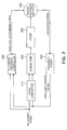
- FIG. 2 is a block diagram illustrating an example of the frequency synthesizer shown in FIG. 1 .
- the example of the frequency synthesizer shown in FIG. 1 will be described in more detail with reference to FIG. 2 .
- the phase-locked loop unit 110 may be implemented as a loop type unit, namely, a phase-locked loop as shown.
- the phase-locked loop unit 110 includes a phase comparator 210, a charge pump 220, a filter 230, a voltage-controlled oscillator 240 and a frequency divider 250.
- the phase comparator 210 receives a reference signal and a frequency-divided signal and compares the phases of the frequencies of the two signals.
- the phase comparator 210 provides an output signal corresponding to the difference in phases between the reference signal and the frequency-divided signal to the charge pump 220.
- the charge pump 220 receives an output signal from the phase comparator 210 and outputs a current corresponding thereto.
- the current output from the charge pump 220 is input to the filter 230, and the filter 230 converts the input current into a voltage so as to provide it to the voltage-controlled oscillator 240.
- the voltage output from the filter 230 may be used as a control signal to the voltage-controlled oscillator 240.
- the voltage-controlled oscillator 240 generates an oscillating signal by adjusting frequency dividing using a control signal output from the filter 230 with reference to a certain frequency gain level.
- the frequency gain level may correspond to a capacitor bank of the voltage-controlled oscillator 240. Accordingly, the voltage-controlled oscillator 240 may use a gain level determining signal provided from the automatic frequency controller 260 to determine a capacitor bank used in oscillating.
- the frequency divider 240 may divide the frequency of an oscillating signal output from the voltage-controlled oscillator 250 at a predetermined proportion.
- the frequency divider 250 may divide the frequency of an oscillating signal so that it has the same frequency with a reference signal, so as to generate a frequency-divided signal.
- the above-described reference signal, oscillating signal and frequency-divided signal may be a voltage signal.
- the automatic frequency control unit 120 may also be implemented as a loop type unit. As shown, the automatic frequency control unit 120 may include the voltage-controlled oscillator 240, a frequency divider 250 and the automatic frequency controller 260.
- the automatic frequency controller 260 receives a reference signal and a frequency-divided signal and detects the difference between the two signals. Then, the automatic frequency control unit 120 determines whether to change the frequency gain level depending on the difference between the two signals, to create a gain level determining signal. The generated gain level determining signal is input to the voltage-controlled oscillator 240.
- FIG. 3 is a graph showing an example of a capacitor bank applicable to a frequency synthesizer
- Table 1 is a look-up table representing the capacitor bank shown in FIG. 3 as a table.
- [Table 1] Cap-bank 0 0.2 0.4 0.6 0.8 1 1.2 1.4 1.6 1.8 1 1000 1002 1004 1006 1008 1010 1012 1014 1016 1018 2 1010 1012 1014 1016 1018 1020 1022 1024 1026 1028 3 1020 1022 1024 1026 1028 1030 1032 1034 1036 1038 4 1030 1032 1034 1036 1038 1040 1042 1044 1046 1048 5 1040 1042 1044 1046 1048 1050 1052 1054 1056 1058 6 1050 1052 1054 1056 1058 1060 1062 1064 1066 1068 7 1060 1062 1064 1066 1068 1070 1072 1074 1076 1078 8 1070 1072 1074 1076 1078 1080 1082 1084 1086 1088 9 1080 1082 1084 1086 10
- the y-axis represents frequency and the x-axis represents a control signal to the voltage-controlled oscillator 240.
- the number of the capacitor banks is 32, and their characteristic according to voltage and frequency is shown.
- the voltage-controlled oscillator 240 is set such that it outputs 1000 MHz when the control signal is 0 V and outputs 1010 MHz when the control signal is 1 V, with the capacitor bank 1.
- the capacitor bank is the 12 th ; the control signal of approximately 1 V may be used.
- an error may cause 1120 MHz to correspond to the 17th of the capacitor banks instead of the 12th.
- the auto frequency controller 260 uses the look-up table to select 12th of the capacitor banks and determines whether it is locked regardless of the error. If it is unlocked, the column of the capacitor banks is incremented by one so as to move to 13th, and it is determined again whether it is locked. Accordingly, the automatic frequency controller 260 repeats the locking process until actual locking is made, that is, repeats six times until 17th column of the capacitor banks is used.
- the frequency may be adjusted by doing the above operation, it takes relatively long locking time. In the above example, all of the columns from 12th to 17th columns are determined whether they are locked. Therefore, six times more locking time is required.
- the embodiments of the present invention performs correction for locking.
- a frequency synthesizer according to an embodiment of the present invention will be described in detail with reference to FIGS. 4 to 6 .
- FIG. 4 is a block diagram for illustrating a frequency synthesizer according to an embodiment of the present invention.
- the frequency synthesizer includes an automatic frequency control unit 410, a phase-locked loop unit 420 and a correction unit 430.
- the automatic frequency control unit 410 sequentially searches a plurality of frequency gain levels, and determines a first gain level corresponding to a phase difference between the frequency of a frequency-divided oscillating signal and the frequency of a reference signal.
- the first gain level is input to the correction unit 430 and used for determining a correction gain level.
- the phase-locked loop unit 420 detects a phase difference between the frequency of a frequency-divided oscillating signal and the frequency of the reference signal.
- the phase-locked loop unit 420 adjusts the frequency dividing of the oscillating signal such that the phase difference becomes smaller within the range of the correction gain level provided from the correction unit 430.
- the correction unit 430 uses the first gain level provided from the automatic frequency control unit 410 to determine the gain correction deviation.
- the correction unit 430 may use the gain correction value to determine the correction gain level.
- the correction unit 430 may determine the gain correction value by reflecting the firs gain level in the input gain level irrespective of the change in the oscillating signal or the reference signal. That is, even if the oscillating signal or reference signal is changed, the gain correction value may have a constant value, and the gain correction value may be determined from the first driving of the phase-locked loop. To this end, the correction unit 430 may determine the gain correction value based on the first gain level by the first operation of the automatic frequency control unit 410, and may reflect the gain correction value from when the automatic frequency control unit 410 operates for the second time.
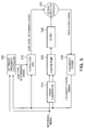
- FIG. 5 is a block diagram illustrating an example of the frequency synthesizer shown in FIG. 4 .
- the example of the frequency synthesizer will be described in more detail with reference to FIG. 5 .
- the phase-locked loop unit 410 may be implemented as a loop type unit, namely, a phase-locked loop.
- the phase-locked loop unit 410 includes a phase comparator 510, a charge pump 520, a filter 530, a voltage-controlled oscillator 540 and a frequency divider 550.
- the phase comparator 510 receives an oscillating signal and a reference signal, and outputs a phase difference between the frequency of the oscillating signal and the frequency of the reference signal.
- the charge pump 520 charges or discharges the capacitor depending on the phase difference output from the phase comparator 510, to output a current corresponding thereto.
- the filter 530 uses a current output from the charge pump 520 to create a control signal, providing it to the voltage-controlled oscillator 540.
- the voltage-controlled oscillator 540 receives the control signal corresponding to the phase difference and oscillates the oscillating signal by reflecting the control signal in the correction gain level.
- the control signal may be a voltage signal.
- the frequency divider 550 may divide the frequency of the oscillating signal output from the voltage-controlled oscillator 540 at a predetermined proportion.
- the automatic frequency control unit 420 may also be implemented as a loop type unit. As shown, the automatic frequency control unit 420 may include the voltage-controlled oscillator 540, the frequency divider 550 and the automatic frequency controller 560.
- the automatic frequency controller 560 receives a reference signal and a frequency-divided signal and detects the difference between the two signals. Then, the automatic frequency control unit 420 may determine whether to change the frequency gain level depending on the difference between the two signals, to create a gain level determining signal. The generated gain level determining signal is input to a corrector 570.
- the correction unit 430 may be implemented as a corrector 570.
- the corrector 570 uses a gain level determining signal to determine a gain correction value.
- the corrector 570 may determine the difference between the first gain level initially determined in the automatic frequency controller 560 and the input gain level as the gain correction value, to store it.
- the corrector 570 may determine the correction gain level by reflecting the stored gain correction value if a new input gain level is input.
- the determined correction gain level is provided to the voltage-controlled oscillator 540 as a correction gain level signal.
- the gain level may be determined using capacitor banks.
- the voltage-controlled oscillator 540 may store a look-up table for a plurality of capacitor banks corresponding to a plurality of frequency gain levels, and may adjust the frequency dividing using a capacitor bank corresponding to the correction gain level.
- the automatic frequency controller 560 may output a capacitor bank value (the first gain level) corresponding to the phase difference between the frequency of the oscillating signal and the frequency of the reference signal.
- the corrector 570 may determine the gain correction value (capacitor bank correction value) from the difference between the look-up table for the capacitor bank and the first gain level (capacitor bank value) by the first operation of the automatic frequency controller 560.
- the corrector 570 may output the correction gain level (the corrected capacitor bank value) by reflecting the calculated capacitor bank correction value in each of the capacitor bank values output from the automatic frequency controller 560. That is, the corrector 570 may determine the correction gain level by reflecting the stored gain correction value in the look-up table from when the automatic frequency controller 560 operates for the second time.
- FIG. 6 is a block diagram illustrating an example of the corrector shown in FIG. 5 .
- the example of the corrector 570 will be described in more detail with reference to FIG. 6 .
- the corrector 570 includes a subtractor 571, a register 572, and an adder 573.
- the subtractor 571 receives a capacitor bank output and a capacitor bank input, to subtract one from the other.
- the capacitor bank output is a capacitor bank value output from an IC
- the capacitor bank input is a value output from the automatic frequency controller 560. Therefore, the value calculated in the subtractor 571 corresponds to the above-described gain correction value.
- the subtractor 571 may use the value when the automatic frequency controller 560 operates for the first time to perform subtraction.
- the subtractor 571 may operate at the time of first locking only. This is because the correction value of the capacitor bank is independent of the number of locking, such that the same correction value detected at the first operation may be used in the later operations.
- the register 572 stores the capacitor bank difference value output from the subtractor 571, that is, the gain correction value.
- the register 572 may provide the output capacitor bank difference value stored therein to the adder 573 whenever the loop of the automatic frequency controller 560 operates one time.
- the adder 573 may add the difference value stored in the register 572 to the capacitor bank output, outputting a capacitor bank correction value (correction gain level).
- the capacitor bank correction value output from the subtractor 573 may correct a frequency error due to an error in a process or a circuit. That is, in the example described with reference to FIG. 3 , after the capacitor banks are sequentially searched for five times in the first loop, the subtractor 571 may determine the value 5 as the correction value.
- the register 572 stores the value of 5, and the subtractor 573 may reflect the correction value of 5 in the every output capacitor bank value of the automatic frequency controller 560.
- FIG. 7 is a flowchart for illustrating a method of controlling a frequency synthesizer according to an embodiment of the present invention.
- the method of controlling the frequency synthesizer includes determining a phase difference between the frequency of a frequency-divided oscillating signal and the frequency of a reference signal (S710).
- a first gain level corresponding to the phase difference is detected by automatic frequency control (S720), and look-up tables of capacitor banks are sequentially searched, so that the input gain level corresponding to the phase difference may be determined (S730).
- the frequency synthesizer may use locking information when the automatic frequency control is initially performed, to determine a first gain level.
- a gain correction value may be calculated based on the difference between the first gain level and the input gain level (S740).
- the frequency synthesizer may reflect the gain correction value in the first gain level by the phase difference due to driving after the automatic frequency control is driven for the second time. Further, the frequency synthesizer may dividing the frequency of the oscillating signal again by reflecting the gain correction value, determining the phase difference based on the oscillating signal which was frequency-divided again (S710).
- FIG. 8 is a graph showing simulation data according to an embodiment of the present invention.
- IN_cap_bank corresponds to an input of the capacitor banks
- OUT_cap_bank in the middle column corresponds to an output of the capacitor banks
- IN_cap_bank ⁇ 5:0> When IN_cap_bank ⁇ 5:0> is changed from 12 to 14 for the first time, namely, when the frequency is changed to 1140 MHz, IN_cap-bank uses 14 (bin:"00 1110") according to the look-up table.
- CAL_cap_bank ⁇ 5:0> exhibits 19 (bin: "01 0011").
- the deviation value is internally searched so that actually the 17th capacitor bank is directly selected. Accordingly, the locking time is not increased even if there is a deviation in an IC, thereby optimizing the locking time in any case.
- a deviation is determined in the first locking process, and the determined deviation is reflected in selecting a capacitor bank to thereby eliminating the sequential locking process. Accordingly, correction can be performed with one time locking, thereby decreasing locking time.
Landscapes
- Stabilization Of Oscillater, Synchronisation, Frequency Synthesizers (AREA)
Abstract
There is provided a frequency synthesizer, including: a phase-locked loop unit detecting a phase difference between a frequency of a frequency-divided oscillating signal and a frequency of a reference signal so as to adjust dividing of the frequency of the oscillating signal so that the phase difference is decreased within a range of the correction gain levels; an automatic frequency control unit sequentially searching a plurality of frequency gain levels so as to determine a first gain level corresponding to the phase difference between the frequency of the frequency-divided oscillating signal and the frequency of the reference signal; and a correction unit determining a gain correction value using the first gain level so as to determine the correction gain level by reflecting the gain correction value.
Description
- This application claims the priority of Korean Patent Application No.
10-2013-0086103 filed on July 22, 2013 - The present invention relates to a frequency synthesizer capable of quickly correcting a deviation in frequency to optimize locking time, and a method of controlling the same.
- In wireless communication technologies, a frequency synthesizer is widely used for generating a stable frequency for signal transmission/reception.
- A commonly used frequency synthesizer is a phase-locked loop (PLL) that includes a voltage-controlled oscillator.
- The phase-locked loop may lock an output frequency of the voltage-controlled oscillator in a feedback control manner, and the voltage-controlled oscillator may use a plurality of capacitor banks to determine an output frequency.
- Existing frequency synthesizers, however, require locking time taken to correct a deviation generated by a producing process and the like.
- In particular, if divided frequencies and the frequency associated with the capacitor banks are different due to an error in a process or in a circuit; locking time is increased for corrections whenever a frequency is divided.
- In order to overcome this shortcoming, an automatic frequency control scheme has been employed for correcting deviations generated due to an error. The auto frequency control scheme requires sequentially searching for frequencies of the capacitor banks in order to set locking due to an error. Therefore, frequency can be correctly locked only after the sequential searching on the capacitor banks is completed, such that locking time for multiple locking is still required.
-
Patent Document 1 relates to an AFC control apparatus, an AFC control method, an AFC control program and a mobile communication apparatus, andPatent Document 2 relates to automatic frequency control apparatus and method. However, the inventions disclosed in the Patent Documents require sequential locking if a matching deviation exists in the capacitor banks due to an error on an IC and the like, and thus still have the shortcoming of increased locking times. -
- (Patent Document 1) Korea Patent Publication No.
10-1073920 - (Patent Document 2) Japanese Patent Laid-Open Publication No.
2008-205703 - An aspect of the present invention provides a frequency synthesizer and a method of controlling the same capable of determining a deviation in the first locking process, and reflecting the determined deviation in selecting a capacitor bank, thereby eliminating the sequential locking process and reducing the locking time.
- According to an aspect of the present invention, there is provided a frequency synthesizer, including: a phase-locked loop unit detecting a phase difference between a frequency of a frequency-divided oscillating signal and a frequency of a reference signal so as to adjust dividing of the frequency of the oscillating signal so that the phase difference is decreased within a range of the correction gain levels; an automatic frequency control unit sequentially searching a plurality of frequency gain levels so as to determine a first gain level corresponding to the phase difference between the frequency of the frequency-divided oscillating signal and the frequency of the reference signal; and a correction unit determining a gain correction value using the first gain level so as to determine the correction gain level by reflecting the gain correction value.
- The phase-locked loop unit may include: a phase comparator receiving the oscillating signal and the reference signal so as to output a phase difference between the frequency of the oscillating signal and the frequency of the reference signal; and a voltage-controlled oscillator receiving a control signal corresponding to the phase difference and adjusting the frequency dividing by reflecting the control signal in the correction gain level so as to oscillate the oscillating signal.
- The voltage-controlled oscillator may store a look-up table for a plurality of capacitor banks corresponding to a plurality of frequency gain levels, and may adjust the frequency dividing using a capacitor bank corresponding to the correction gain level.
- The correction unit may determine a difference between the first gain level initially determined in the automatic frequency control unit and the input gain level as the gain correction value, and store it.
- The corrector may determine the correction gain level by reflecting the stored gain correction value if a new input gain level is input.
- The phase-locked loop may include: a charge pump charging or discharging capacitors according to the phase difference output from the phase comparator; and a filter generating the control signal using a current output from the charge pump.
- According to another aspect of the present invention, there is provided a frequency synthesizer, including: a phase-locked loop detecting a phase difference between a frequency of a frequency-divided oscillating signal and a frequency of a reference signal so as to adjust dividing of the frequency of the oscillating signal so that the phase difference is decreased within a range of the correction gain levels; an automatic frequency control unit searching a plurality of frequency gain levels so as to determine a first gain level corresponding to the phase difference between the frequency of the frequency-divided oscillating signal and the frequency of the reference signal; and a correction unit determining a gain correction value based on the first gain level by a first operation of the automatic frequency control unit, and reflecting the gain correction value after second operation of the automatic frequency control unit.
- The phase-locked loop unit may include: a phase comparator receiving the oscillating signal and the reference signal so as to output a phase difference between the frequency of the oscillating signal and the frequency of the reference signal; and a voltage-controlled oscillator receiving a control signal corresponding to the phase difference and adjusting the frequency dividing by reflecting the control signal in the correction gain level so as to oscillate the oscillating signal.
- The voltage-controlled oscillator may store a look-up table for a plurality of capacitor banks corresponding to a plurality of frequency gain levels, and may adjust the frequency dividing using a capacitor bank corresponding to the correction gain level.
- The correction unit may determine the gain correction value from a difference between a look-up table for the capacitor bank and the first gain level by the first operation.
- The correction unit may determine the correction gain level by reflecting the gain correction value in the look-up table from when the automatic frequency control unit operates for the second time.
- The phase-locked loop may include: a charge pump charging or discharging capacitors according to the phase difference output from the phase comparator; and a filter generating the control signal using a current output from the charge pump.
- According to another aspect of the present invention, there is provided a method of controlling a frequency synthesizer using capacitor banks, the method including: determining a phase difference between a frequency of a frequency-divided oscillating signal and a frequency of a reference signal; detecting a first gain level corresponding to the phase difference through automatic frequency control; sequentially searching look-up tables for capacitor banks to determine an input gain level corresponding to the phase difference; and calculating a gain correction value from the difference between the first gain level and the input gain level.
- The detecting of the first gain level may include determining the first gain level using locking information when the automatic frequency control is operated for the first time.
- The method may further include reflecting the gain correction value in the first gain level by the phase difference by the operation from when the automatic frequency control is operated for the second time.
- The method may further include dividing the frequency of the oscillating signal again by reflecting the gain correction value, so as to perform the determining of the phase difference again based on the oscillating signal which was frequency-divided again.
- The above and other aspects, features and other advantages of the present invention will be more clearly understood from the following detailed description taken in conjunction with the accompanying drawings, in which:
-
FIG. 1 is a block diagram for illustrating an example of a typical frequency synthesizer; -
FIG. 2 is a block diagram for illustrating an example of the frequency synthesizer shown inFIG. 1 ; -
FIG. 3 is a graph showing an example of a capacitor bank applicable to a frequency synthesizer; -
FIG. 4 is a block diagram for illustrating a frequency synthesizer according to an embodiment of the present invention; -
FIG. 5 is a block diagram for illustrating an example of the frequency synthesizer shown inFIG. 4 ; -
FIG. 6 is a block diagram for illustrating an example of the corrector shown inFIG. 5 ; -
FIG. 7 is a flowchart for illustrating a method of controlling a frequency synthesizer according to an embodiment of the present invention; and -
FIG. 8 is a graph showing simulation data according to an embodiment of the present invention. - Hereinafter, embodiments of the present invention will be described in detail with reference to the accompanying drawings. The invention may, however, be embodied in many different forms and should not be construed as being limited to the embodiments set forth herein. Rather, these embodiments are provided so that this disclosure will be thorough and complete, and will fully convey the scope of the invention to those skilled in the art. Throughout the drawings, the same or like reference numerals will be used to designate the same or like elements.
-
FIG. 1 is a block diagram for illustrating an example of a frequency synthesizer. - Referring to
FIG. 1 , the frequency synthesizer includes a phase-lockedloop unit 110 and an automaticfrequency control unit 120. - The phase-locked
loop unit 110 detects a phase difference between a previous oscillating signal and a reference signal, and generates a current oscillating signal by adjusting frequency dividing so that the phase difference is decreased. Here, the generated oscillating signal is fed back to the phase-lockedloop unit 110. - In adjusting frequency dividing, the phase-locked
loop unit 110 may use a predetermined gain level to adjust frequency dividing. The gain level may be determined based on the information provided from the automaticfrequency control unit 120. - The automatic
frequency control unit 120 generates a gain level determining signal to maintain or change the current frequency gain level depending on the difference in phases between the frequency of the oscillating signal frequency-divided from the phase-lockedloop unit 110 and the frequency of the reference signal. The automaticfrequency control unit 120 may provide the generated gain level determining signal to the phase-lockedloop unit 110. The phase-lockedloop unit 110 may determine the gain level depending on the gain level determining signal and may adjust frequency dividing using the determined gain level. -
FIG. 2 is a block diagram illustrating an example of the frequency synthesizer shown inFIG. 1 . In the following, the example of the frequency synthesizer shown inFIG. 1 will be described in more detail with reference toFIG. 2 . - Referring to
FIGS. 1 and2 , the phase-lockedloop unit 110 may be implemented as a loop type unit, namely, a phase-locked loop as shown. The phase-lockedloop unit 110 includes aphase comparator 210, acharge pump 220, afilter 230, a voltage-controlledoscillator 240 and afrequency divider 250. - The
phase comparator 210 receives a reference signal and a frequency-divided signal and compares the phases of the frequencies of the two signals. Thephase comparator 210 provides an output signal corresponding to the difference in phases between the reference signal and the frequency-divided signal to thecharge pump 220. - The
charge pump 220 receives an output signal from thephase comparator 210 and outputs a current corresponding thereto. The current output from thecharge pump 220 is input to thefilter 230, and thefilter 230 converts the input current into a voltage so as to provide it to the voltage-controlledoscillator 240. Here, the voltage output from thefilter 230 may be used as a control signal to the voltage-controlledoscillator 240. - The voltage-controlled
oscillator 240 generates an oscillating signal by adjusting frequency dividing using a control signal output from thefilter 230 with reference to a certain frequency gain level. - Here, the frequency gain level may correspond to a capacitor bank of the voltage-controlled
oscillator 240. Accordingly, the voltage-controlledoscillator 240 may use a gain level determining signal provided from theautomatic frequency controller 260 to determine a capacitor bank used in oscillating. - The
frequency divider 240 may divide the frequency of an oscillating signal output from the voltage-controlledoscillator 250 at a predetermined proportion. For example, thefrequency divider 250 may divide the frequency of an oscillating signal so that it has the same frequency with a reference signal, so as to generate a frequency-divided signal. Here, the above-described reference signal, oscillating signal and frequency-divided signal may be a voltage signal. - The automatic
frequency control unit 120 may also be implemented as a loop type unit. As shown, the automaticfrequency control unit 120 may include the voltage-controlledoscillator 240, afrequency divider 250 and theautomatic frequency controller 260. - The
automatic frequency controller 260 receives a reference signal and a frequency-divided signal and detects the difference between the two signals. Then, the automaticfrequency control unit 120 determines whether to change the frequency gain level depending on the difference between the two signals, to create a gain level determining signal. The generated gain level determining signal is input to the voltage-controlledoscillator 240. - The specific operation of the
automatic frequency controller 260 will be described in detail with reference toFIG. 3 and Table 1 below. -
FIG. 3 is a graph showing an example of a capacitor bank applicable to a frequency synthesizer, and Table 1 is a look-up table representing the capacitor bank shown inFIG. 3 as a table.[Table 1] Cap-bank 0 0.2 0.4 0.6 0.8 1 1.2 1.4 1.6 1.8 1 1000 1002 1004 1006 1008 1010 1012 1014 1016 1018 2 1010 1012 1014 1016 1018 1020 1022 1024 1026 1028 3 1020 1022 1024 1026 1028 1030 1032 1034 1036 1038 4 1030 1032 1034 1036 1038 1040 1042 1044 1046 1048 5 1040 1042 1044 1046 1048 1050 1052 1054 1056 1058 6 1050 1052 1054 1056 1058 1060 1062 1064 1066 1068 7 1060 1062 1064 1066 1068 1070 1072 1074 1076 1078 8 1070 1072 1074 1076 1078 1080 1082 1084 1086 1088 9 1080 1082 1084 1086 1088 1090 1092 1094 1096 1098 10 1090 1092 1094 1096 1098 1100 1102 1104 1106 1108 11 1100 1102 1104 1106 1108 1110 1112 1114 1116 1118 12 1110 1112 1114 1116 1118 1120 1122 1124 1126 1128 13 1120 1122 1124 1126 1128 1130 1132 1134 1136 1138 14 1130 1132 1134 1136 1138 1140 1142 1144 1146 1148 15 1140 1142 1144 1146 1148 1150 1152 1154 1156 1158 16 1150 1152 1154 1156 1158 1160 1162 1164 1166 1168 17 1160 1162 1164 1166 1168 1170 1172 1174 1176 1178 18 1170 1172 1174 1176 1178 1180 1182 1184 1186 1188 19 1180 1182 11.84 1186 1188 1190 1192 1194 1196 1198 20 1190 1192 1194 1196 1198 1200 1202 1204 1206 1208 21 1200 1202 1204 1206 1208 1210 1212 1214 1216 1218 22 1210 1212 1214 1216 1218 1220 1222 1224 1226 1228 23 1220 1222 1224 1226 1228 1230 1232 1234 1236 1238 24 1230 1232 1234 1236 1238 1240 1242 1244 1246 1248 25 1240 1242 1244 1246 1248 1250 1252 1254 1256 1258 26 1250 1252 1254 1256 1258 1260 1262 1264 1266 1268 27 1260 1262 1264 1266 1268 1270 1272 1274 1276 1278 28 1270 1272 1274 1276 1278 1280 1282 1284 1286 1288 29 1280 1282 1284 1286 1288 1290 1292 1294 1296 1298 30 1290 1292 1294 1296 1298 1300 1302 1304 1306 1308 31 1300 1302 1304 1306 1308 1310 1312 1314 1316 1318 32 1310 1312 1314 1316 1318 1320 1322 1324 1326 1328 - In
FIG. 3 , the y-axis represents frequency and the x-axis represents a control signal to the voltage-controlledoscillator 240. In the shown example, the number of the capacitor banks is 32, and their characteristic according to voltage and frequency is shown. - In the shown example, the voltage-controlled
oscillator 240 is set such that it outputs 1000 MHz when the control signal is 0 V and outputs 1010 MHz when the control signal is 1 V, with thecapacitor bank 1. Here, if a target frequency is 1120 MHz, the capacitor bank is the 12th; the control signal of approximately 1 V may be used. - However, due to a processing error or an issue related to a circuit, the characteristic of the capacitor bank to frequency may be changed. In this case, there is a problem in that the loop should be driven multiple times for frequency locking.
- For example, an error may cause 1120 MHz to correspond to the 17th of the capacitor banks instead of the 12th. In this case, the
auto frequency controller 260 uses the look-up table to select 12th of the capacitor banks and determines whether it is locked regardless of the error. If it is unlocked, the column of the capacitor banks is incremented by one so as to move to 13th, and it is determined again whether it is locked. Accordingly, theautomatic frequency controller 260 repeats the locking process until actual locking is made, that is, repeats six times until 17th column of the capacitor banks is used. - Although the frequency may be adjusted by doing the above operation, it takes relatively long locking time. In the above example, all of the columns from 12th to 17th columns are determined whether they are locked. Therefore, six times more locking time is required.
- In order to prevent the locking time from increasing, the embodiments of the present invention performs correction for locking. In the following, a frequency synthesizer according to an embodiment of the present invention will be described in detail with reference to
FIGS. 4 to 6 . - In the following descriptions, an overlapped description for contents that are the same as or correspond to contents described above with reference to
FIGS. 1 and2 will be omitted. -
FIG. 4 is a block diagram for illustrating a frequency synthesizer according to an embodiment of the present invention. - Referring to
FIG. 4 , the frequency synthesizer according to the embodiment includes an automaticfrequency control unit 410, a phase-lockedloop unit 420 and acorrection unit 430. - The automatic
frequency control unit 410 sequentially searches a plurality of frequency gain levels, and determines a first gain level corresponding to a phase difference between the frequency of a frequency-divided oscillating signal and the frequency of a reference signal. Here, the first gain level is input to thecorrection unit 430 and used for determining a correction gain level. - The phase-locked
loop unit 420 detects a phase difference between the frequency of a frequency-divided oscillating signal and the frequency of the reference signal. The phase-lockedloop unit 420 adjusts the frequency dividing of the oscillating signal such that the phase difference becomes smaller within the range of the correction gain level provided from thecorrection unit 430. - The
correction unit 430 uses the first gain level provided from the automaticfrequency control unit 410 to determine the gain correction deviation. Thecorrection unit 430 may use the gain correction value to determine the correction gain level. - In an embodiment, the
correction unit 430 may determine the gain correction value by reflecting the firs gain level in the input gain level irrespective of the change in the oscillating signal or the reference signal. That is, even if the oscillating signal or reference signal is changed, the gain correction value may have a constant value, and the gain correction value may be determined from the first driving of the phase-locked loop. To this end, thecorrection unit 430 may determine the gain correction value based on the first gain level by the first operation of the automaticfrequency control unit 410, and may reflect the gain correction value from when the automaticfrequency control unit 410 operates for the second time. -
FIG. 5 is a block diagram illustrating an example of the frequency synthesizer shown inFIG. 4 . In the following, the example of the frequency synthesizer will be described in more detail with reference toFIG. 5 . - Referring to
FIGS. 4 and5 , the phase-lockedloop unit 410 may be implemented as a loop type unit, namely, a phase-locked loop. The phase-lockedloop unit 410 includes aphase comparator 510, acharge pump 520, afilter 530, a voltage-controlledoscillator 540 and afrequency divider 550. - The
phase comparator 510 receives an oscillating signal and a reference signal, and outputs a phase difference between the frequency of the oscillating signal and the frequency of the reference signal. Thecharge pump 520 charges or discharges the capacitor depending on the phase difference output from thephase comparator 510, to output a current corresponding thereto. Thefilter 530 uses a current output from thecharge pump 520 to create a control signal, providing it to the voltage-controlledoscillator 540. The voltage-controlledoscillator 540 receives the control signal corresponding to the phase difference and oscillates the oscillating signal by reflecting the control signal in the correction gain level. Here, the control signal may be a voltage signal. Thefrequency divider 550 may divide the frequency of the oscillating signal output from the voltage-controlledoscillator 540 at a predetermined proportion. - The automatic
frequency control unit 420 may also be implemented as a loop type unit. As shown, the automaticfrequency control unit 420 may include the voltage-controlledoscillator 540, thefrequency divider 550 and theautomatic frequency controller 560. - The
automatic frequency controller 560 receives a reference signal and a frequency-divided signal and detects the difference between the two signals. Then, the automaticfrequency control unit 420 may determine whether to change the frequency gain level depending on the difference between the two signals, to create a gain level determining signal. The generated gain level determining signal is input to acorrector 570. - The
correction unit 430 may be implemented as acorrector 570. Thecorrector 570 uses a gain level determining signal to determine a gain correction value. - The
corrector 570 may determine the difference between the first gain level initially determined in theautomatic frequency controller 560 and the input gain level as the gain correction value, to store it. Thecorrector 570 may determine the correction gain level by reflecting the stored gain correction value if a new input gain level is input. The determined correction gain level is provided to the voltage-controlledoscillator 540 as a correction gain level signal. - In an embodiment, the gain level may be determined using capacitor banks. In the embodiment, the voltage-controlled
oscillator 540 may store a look-up table for a plurality of capacitor banks corresponding to a plurality of frequency gain levels, and may adjust the frequency dividing using a capacitor bank corresponding to the correction gain level. - In addition, the
automatic frequency controller 560 may output a capacitor bank value (the first gain level) corresponding to the phase difference between the frequency of the oscillating signal and the frequency of the reference signal. - The
corrector 570 may determine the gain correction value (capacitor bank correction value) from the difference between the look-up table for the capacitor bank and the first gain level (capacitor bank value) by the first operation of theautomatic frequency controller 560. - Then, the
corrector 570 may output the correction gain level (the corrected capacitor bank value) by reflecting the calculated capacitor bank correction value in each of the capacitor bank values output from theautomatic frequency controller 560. That is, thecorrector 570 may determine the correction gain level by reflecting the stored gain correction value in the look-up table from when theautomatic frequency controller 560 operates for the second time. -
FIG. 6 is a block diagram illustrating an example of the corrector shown inFIG. 5 . In the following, the example of thecorrector 570 will be described in more detail with reference toFIG. 6 . - Referring to
FIG. 6 , thecorrector 570 includes asubtractor 571, aregister 572, and anadder 573. - The
subtractor 571 receives a capacitor bank output and a capacitor bank input, to subtract one from the other. Here, the capacitor bank output is a capacitor bank value output from an IC, and the capacitor bank input is a value output from theautomatic frequency controller 560. Therefore, the value calculated in thesubtractor 571 corresponds to the above-described gain correction value. - In an embodiment, the
subtractor 571 may use the value when theautomatic frequency controller 560 operates for the first time to perform subtraction. Thesubtractor 571 may operate at the time of first locking only. This is because the correction value of the capacitor bank is independent of the number of locking, such that the same correction value detected at the first operation may be used in the later operations. - The
register 572 stores the capacitor bank difference value output from thesubtractor 571, that is, the gain correction value. Theregister 572 may provide the output capacitor bank difference value stored therein to theadder 573 whenever the loop of theautomatic frequency controller 560 operates one time. - The
adder 573 may add the difference value stored in theregister 572 to the capacitor bank output, outputting a capacitor bank correction value (correction gain level). - Accordingly, the capacitor bank correction value output from the
subtractor 573 may correct a frequency error due to an error in a process or a circuit. That is, in the example described with reference toFIG. 3 , after the capacitor banks are sequentially searched for five times in the first loop, thesubtractor 571 may determine thevalue 5 as the correction value. Theregister 572 stores the value of 5, and thesubtractor 573 may reflect the correction value of 5 in the every output capacitor bank value of theautomatic frequency controller 560. By doing so, in the embodiment of the present invention, locking time is required only in the first operation and lock may be immediately performed from the second time. -
FIG. 7 is a flowchart for illustrating a method of controlling a frequency synthesizer according to an embodiment of the present invention. - The method illustrated in
FIG. 7 will be described with respect to the frequency synthesizer described with reference toFIGS. 4 to 6 , and, therefore, descriptions on the same elements as those described above will not be repeated. - The method of controlling the frequency synthesizer includes determining a phase difference between the frequency of a frequency-divided oscillating signal and the frequency of a reference signal (S710).
- Then, a first gain level corresponding to the phase difference is detected by automatic frequency control (S720), and look-up tables of capacitor banks are sequentially searched, so that the input gain level corresponding to the phase difference may be determined (S730).
- In the embodiment in operation S730, the frequency synthesizer may use locking information when the automatic frequency control is initially performed, to determine a first gain level.
- Then, a gain correction value may be calculated based on the difference between the first gain level and the input gain level (S740).
- Additionally, the frequency synthesizer may reflect the gain correction value in the first gain level by the phase difference due to driving after the automatic frequency control is driven for the second time. Further, the frequency synthesizer may dividing the frequency of the oscillating signal again by reflecting the gain correction value, determining the phase difference based on the oscillating signal which was frequency-divided again (S710).
-
FIG. 8 is a graph showing simulation data according to an embodiment of the present invention. - IN_cap_bank corresponds to an input of the capacitor banks, and OUT_cap_bank in the middle column corresponds to an output of the capacitor banks.
- It can be seen from the data in the left column that IN_cap_bank<5:0> initially selects 12th (bin:"00 1100") capacitor bank, and it can be seen from the data in the middle column that OUT_cap_bank<5:0> outputs 17 (bin:"01 0001"). In the data in the right column, CAL_cap_bank<5:0> outputs 17 (bin:"01 0001").
- When IN_cap_bank<5:0> is changed from 12 to 14 for the first time, namely, when the frequency is changed to 1140 MHz, IN_cap-bank uses 14 (bin:"00 1110") according to the look-up table. Here, it can be seen that CAL_cap_bank<5:0> exhibits 19 (bin: "01 0011").
- In the related art, when the frequency is changed to 1140 MHz, 14 is input to IN_cap_bank<5:0> so as to repeat a predetermined locking process, and thus the AFC block sequentially searches the capacitor banks in the order of from 12 to 17, thereby increasing the overall locking time.
- According to the embodiment of the present invention, however, although 1140 MHz is the 12th capacitor bank in the look-up table as shown in the result of the simulation, the deviation value is internally searched so that actually the 17th capacitor bank is directly selected. Accordingly, the locking time is not increased even if there is a deviation in an IC, thereby optimizing the locking time in any case.
- As set forth above, according to the embodiments of the present invention, a deviation is determined in the first locking process, and the determined deviation is reflected in selecting a capacitor bank to thereby eliminating the sequential locking process. Accordingly, correction can be performed with one time locking, thereby decreasing locking time.
- While the present invention has been shown and described in connection with the embodiments, it will be apparent to those skilled in the art that modifications and variations can be made without departing from the spirit and scope of the invention as defined by the appended claims.
Claims (16)
- A frequency synthesizer, comprising:a phase-locked loop unit detecting a phase difference between a frequency of a frequency-divided oscillating signal and a frequency of a reference signal so as to adjust dividing of the frequency of the oscillating signal so that the phase difference is decreased within a range of the correction gain levels;an automatic frequency control unit sequentially searching a plurality of frequency gain levels so as to determine a first gain level corresponding to the phase difference between the frequency of the frequency-divided oscillating signal and the frequency of the reference signal; anda correction unit determining a gain correction value using the first gain level so as to determine the correction gain level by reflecting the gain correction value.
- The synthesizer of claim 1, wherein the phase-locked loop unit includes:a phase comparator receiving the oscillating signal and the reference signal so as to output a phase difference between the frequency of the oscillating signal and the frequency of the reference signal; anda voltage-controlled oscillator receiving a control signal corresponding to the phase difference and adjusting the frequency dividing by reflecting the control signal in the correction gain level so as to oscillate the oscillating signal.
- The synthesizer of claim 2, wherein the voltage-controlled oscillator stores look-up tables for a plurality of capacitor banks corresponding to the plurality of frequency gain levels, and adjusts the frequency dividing using a capacitor bank corresponding to the correction gain level.
- The synthesizer of claim 1, wherein the correction unit determines a difference between the first gain level initially determined in the automatic frequency control unit and the input gain level as the gain correction value, and stores it.
- The synthesizer of claim 4, wherein the correction unit determines the correction gain level by reflecting the stored gain correction value when a new input gain level is input.
- The synthesizer of claim 2, wherein the phase-locked loop includes:a charge pump charging or discharging capacitors according to the phase difference output from the phase comparator; anda filter generating the control signal using a current output from the charge pump.
- A frequency synthesizer, comprising:a phase-locked loop detecting a phase difference between a frequency of a frequency-divided oscillating signal and a frequency of a reference signal so as to adjust dividing of the frequency of the oscillating signal so that the phase difference is decreased within a range of the correction gain levels;an automatic frequency control unit searching a plurality of frequency gain levels so as to determine a first gain level corresponding to the phase difference between the frequency of the frequency-divided oscillating signal and the frequency of the reference signal; anda correction unit determining a gain correction value based on the first gain level by a first operation of the automatic frequency control unit, and reflecting the gain correction value from when the automatic frequency control unit operates for the second time.
- The synthesizer of claim 7, wherein the phase-locked loop unit includes:a phase comparator receiving the oscillating signal and the reference signal so as to output a phase difference between the frequency of the oscillating signal and the frequency of the reference signal; anda voltage-controlled oscillator receiving a control signal corresponding to the phase difference and adjusting the frequency dividing by reflecting the control signal in the correction gain level so as to oscillate the oscillating signal.
- The synthesizer of claim 8, wherein the voltage-controlled oscillator stores look-up tables for a plurality of capacitor banks corresponding to the plurality of frequency gain levels, and adjusts the frequency dividing using a capacitor bank corresponding to the correction gain level.
- The synthesizer of claim 8, wherein the correction unit determines the gain correction value from a difference between a look-up table for the capacitor bank and the first gain level by the first operation.
- The synthesizer of claim 10, wherein the correction unit determines the correction gain level by reflecting the gain correction value in the look-up table from when the automatic frequency control unit operates for the second time.
- The synthesizer of claim 8, wherein the phase-locked loop includes:a charge pump charging or discharging capacitors according to the phase difference output from the phase comparator; anda filter generating the control signal using a current output from the charge pump.
- A method of controlling a frequency synthesizer using capacitor banks, the method comprising:determining a phase difference between a frequency of a frequency-divided oscillating signal and a frequency of a reference signal;detecting a first gain level corresponding to the phase difference through automatic frequency control;sequentially searching look-up tables for capacitor banks to determine an input gain level corresponding to the phase difference; andcalculating a gain correction value from the difference between the first gain level and the input gain level.
- The method of claim 13, wherein the detecting of the first gain level includes determining the first gain level using locking information when the automatic frequency control is operated for the first time.
- The method of claim 14, further comprising reflecting the gain correction value in the first gain level by the phase difference by the operation from when the automatic frequency control is operated for the second time.
- The method of claim 15, further comprising dividing the frequency of the oscillating signal again by reflecting the gain correction value, so as to perform the determining of the phase difference again based on the oscillating signal which was frequency-divided again.
Applications Claiming Priority (1)
| Application Number | Priority Date | Filing Date | Title |
|---|---|---|---|
| KR20130086103A KR101462799B1 (en) | 2013-07-22 | 2013-07-22 | Frequency synthesizer and control method using the same |
Publications (1)
| Publication Number | Publication Date |
|---|---|
| EP2830223A1 true EP2830223A1 (en) | 2015-01-28 |
Family
ID=49546360
Family Applications (1)
| Application Number | Title | Priority Date | Filing Date |
|---|---|---|---|
| EP13275259.3A Withdrawn EP2830223A1 (en) | 2013-07-22 | 2013-10-28 | Frequency synthesizer and method of controlling the same |
Country Status (2)
| Country | Link |
|---|---|
| EP (1) | EP2830223A1 (en) |
| KR (1) | KR101462799B1 (en) |
Citations (4)
| Publication number | Priority date | Publication date | Assignee | Title |
|---|---|---|---|---|
| JP2008205703A (en) | 2007-02-19 | 2008-09-04 | Nec Network & Sensor Systems Ltd | Afc controller, afc control method, afc control program, and mobile communication apparatus |
| US7804367B2 (en) * | 2006-10-20 | 2010-09-28 | Fci Inc. | Frequency synthesizer and frequency calibration method |
| US20110032011A1 (en) * | 2009-08-10 | 2011-02-10 | Samsung Electro-Mechanics Co.,Ltd. | Auto frequency calibrator, method thereof and frequency synthesizer using it |
| KR101073920B1 (en) | 2005-11-17 | 2011-10-17 | 엘지전자 주식회사 | apparatus and method for automatic frequency control |
Family Cites Families (3)
| Publication number | Priority date | Publication date | Assignee | Title |
|---|---|---|---|---|
| KR100723838B1 (en) * | 2004-12-08 | 2007-05-31 | 한국전자통신연구원 | Apparatus for frequency synthesizer |
| KR101030499B1 (en) | 2008-12-24 | 2011-04-21 | 전자부품연구원 | Broadband Frequency Synthesizer and Its Synthesis Method |
| KR101209030B1 (en) * | 2010-05-18 | 2012-12-06 | 광운대학교 산학협력단 | Frequency Synthesizer and Fast Automatic Calibration Device therefor |
-
2013
- 2013-07-22 KR KR20130086103A patent/KR101462799B1/en not_active Expired - Fee Related
- 2013-10-28 EP EP13275259.3A patent/EP2830223A1/en not_active Withdrawn
Patent Citations (4)
| Publication number | Priority date | Publication date | Assignee | Title |
|---|---|---|---|---|
| KR101073920B1 (en) | 2005-11-17 | 2011-10-17 | 엘지전자 주식회사 | apparatus and method for automatic frequency control |
| US7804367B2 (en) * | 2006-10-20 | 2010-09-28 | Fci Inc. | Frequency synthesizer and frequency calibration method |
| JP2008205703A (en) | 2007-02-19 | 2008-09-04 | Nec Network & Sensor Systems Ltd | Afc controller, afc control method, afc control program, and mobile communication apparatus |
| US20110032011A1 (en) * | 2009-08-10 | 2011-02-10 | Samsung Electro-Mechanics Co.,Ltd. | Auto frequency calibrator, method thereof and frequency synthesizer using it |
Also Published As
| Publication number | Publication date |
|---|---|
| KR101462799B1 (en) | 2014-11-20 |
Similar Documents
| Publication | Publication Date | Title |
|---|---|---|
| KR101199780B1 (en) | Apparatus and method for frequency calibration in frequency synthesizer | |
| CN101227189B (en) | Frequency synthesizer, automatic frequency correction circuit and frequency correction method | |
| CN103609023B (en) | For adjusting the apparatus and method of voltage-controlled oscillator gain | |
| US8487707B2 (en) | Frequency synthesizer | |
| US5661440A (en) | PLL frequency synthesizer employing plural control frequencies to minimize overshoot | |
| CN112292815A (en) | Compensating for frequency variations of crystal oscillators and related systems, methods, and apparatus | |
| KR102375949B1 (en) | Apparatus and method for controlling output of frequency synthesizer | |
| JP4625849B2 (en) | Oscillator control device | |
| CN112234981A (en) | Data and Clock Recovery Circuitry | |
| US9356612B2 (en) | Method and apparatus to calibrate frequency synthesizer | |
| US7583773B2 (en) | Frequency synthesizing device with automatic calibration | |
| US10218367B2 (en) | Frequency synthesizing device and automatic calibration method thereof | |
| US9966963B2 (en) | Frequency synthesizer | |
| EP2647127B1 (en) | Phase-locked loop control voltage determination | |
| KR101692112B1 (en) | Frequency calibration method and apparatus with frequency synthesizer | |
| KR101462799B1 (en) | Frequency synthesizer and control method using the same | |
| JP2012205137A (en) | Pll circuit | |
| US20230092151A1 (en) | Semiconductor integrated circuit, electronic device, and frequency detecting method | |
| KR102059630B1 (en) | Method and device for controlling output frequency of voltage controlled oscillator | |
| CN110535462B (en) | Digital phase-locked loop with automatic correction function and automatic correction method thereof | |
| JP5722733B2 (en) | PLL circuit and calibration method thereof | |
| KR101710717B1 (en) | Frequency calibration method and apparatus with frequency synthesizer | |
| JP4427428B2 (en) | PLL circuit | |
| US20260066907A1 (en) | Phase-locked loop working system | |
| US6486741B2 (en) | Precise phase comparison even with fractional frequency division ratio |
Legal Events
| Date | Code | Title | Description |
|---|---|---|---|
| 17P | Request for examination filed |
Effective date: 20131028 |
|
| AK | Designated contracting states |
Kind code of ref document: A1 Designated state(s): AL AT BE BG CH CY CZ DE DK EE ES FI FR GB GR HR HU IE IS IT LI LT LU LV MC MK MT NL NO PL PT RO RS SE SI SK SM TR |
|
| AX | Request for extension of the european patent |
Extension state: BA ME |
|
| PUAI | Public reference made under article 153(3) epc to a published international application that has entered the european phase |
Free format text: ORIGINAL CODE: 0009012 |
|
| STAA | Information on the status of an ep patent application or granted ep patent |
Free format text: STATUS: THE APPLICATION HAS BEEN WITHDRAWN |
|
| 18W | Application withdrawn |
Effective date: 20151118 |